ICGOO在线商城 > TLV71736PDQNR
 Datasheet下载
- 型号: TLV71736PDQNR
- 制造商: Texas Instruments
- 库位|库存: xxxx|xxxx
- 要求:
| 数量阶梯 | 香港交货 | 国内含税 |
| +xxxx | $xxxx | ¥xxxx |
查看当月历史价格
查看今年历史价格
TLV71736PDQNR产品简介:
ICGOO电子元器件商城为您提供TLV71736PDQNR由Texas Instruments设计生产,在icgoo商城现货销售,并且可以通过原厂、代理商等渠道进行代购。 提供TLV71736PDQNR价格参考¥0.58-¥1.68以及Texas InstrumentsTLV71736PDQNR封装/规格参数等产品信息。 你可以下载TLV71736PDQNR参考资料、Datasheet数据手册功能说明书, 资料中有TLV71736PDQNR详细功能的应用电路图电压和使用方法及教程。
| 参数 | 数值 |
| 产品目录 | 集成电路 (IC) |
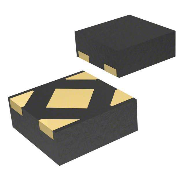
| 描述 | IC REG LDO 3.6V 0.15A 4X2SON |
| 产品分类 | |
| 品牌 | Texas Instruments |
| 数据手册 | |
| 产品图片 |
|
| 产品型号 | TLV71736PDQNR |
| rohs | 无铅 / 符合限制有害物质指令(RoHS)规范要求 |
| 产品系列 | - |
| 供应商器件封装 | 4-X2SON (1x1) |
| 其它名称 | 296-30491-6 |
| 包装 | Digi-Reel® |
| 安装类型 | 表面贴装 |
| 封装/外壳 | 4-XDFN 裸露焊盘 |
| 工作温度 | -40°C ~ 85°C |
| 标准包装 | 1 |
| 电压-跌落(典型值) | 0.215V @ 150mA |
| 电压-输入 | 最高 5.5V |
| 电压-输出 | 3.6V |
| 电流-输出 | 150mA |
| 电流-限制(最小值) | - |
| 稳压器拓扑 | 正,固定式 |
| 稳压器数 | 1 |


- 商务部:美国ITC正式对集成电路等产品启动337调查
- 曝三星4nm工艺存在良率问题 高通将骁龙8 Gen1或转产台积电
- 太阳诱电将投资9.5亿元在常州建新厂生产MLCC 预计2023年完工
- 英特尔发布欧洲新工厂建设计划 深化IDM 2.0 战略
- 台积电先进制程称霸业界 有大客户加持明年业绩稳了
- 达到5530亿美元!SIA预计今年全球半导体销售额将创下新高
- 英特尔拟将自动驾驶子公司Mobileye上市 估值或超500亿美元
- 三星加码芯片和SET,合并消费电子和移动部门,撤换高东真等 CEO
- 三星电子宣布重大人事变动 还合并消费电子和移动部门
- 海关总署:前11个月进口集成电路产品价值2.52万亿元 增长14.8%


PDF Datasheet 数据手册内容提取
Product Order Technical Tools & Support & Folder Now Documents Software Community TLV717P SBVS176B–OCTOBER2011–REVISEDAPRIL2016 TLV717P 150-mA, Low-Dropout Regulator With Foldback Current Limit for Portable Devices 1 Features 3 Description • VeryLowDropout:215mVat150mA The TLV717P series of low-dropout (LDO) linear 1 regulators are low quiescent current LDOs with • Accuracy:0.5%(typical) excellent line and load transient performance and are • LowIQ:35µA designed for power-sensitive applications. These • AvailableinFixed-OutputVoltages: devicesprovideatypicalaccuracyof0.5%. 1.2Vto5V The TLV717P series offer current foldback that • HighPSRR: throttles down the output current with a decrease in load resistance. The typical value at which current – 70dBat1kHz foldback initiates is 350 mA; the typical value of the – 50dBat1MHz outputshortcurrentlimitvalueis40mA. • StableWithEffectiveOutputCapacitance: Furthermore, these devices are stable with an 0.1 µF effective output capacitance of only 0.1 µF. This • FoldbackCurrentLimit feature enables the use of cost-effective capacitors • Package:1-mm×1-mmDQN that have higher bias voltages and temperature derating. The devices regulate to specified accuracy (1) SeethePackageOptionAddendumattheendofthis withnooutputload. documentforacompletelistofavailablevoltageoptions. (2) SeeInputandOutputCapacitorRequirementsformore The TLV717P series is available in a 1-mm × 1-mm details. DQN package that makes them ideal for hand-held applications. The TLV717P provides an active 2 Applications pulldowncircuittoquicklydischargeoutputloads. • PCsandNotebooks DeviceInformation(1) • SmartPhones PARTNUMBER PACKAGE BODYSIZE(NOM) • PortableElectronicsandBattery-PoweredDevices TLV717P X2SON(4) 1.00mm×1.00mm • ElectronicPointofSale (1) For all available packages, see the orderable addendum at theendofthedatasheet. TypicalApplicationCircuit VIN IN OUT VOUT 1mF CIN COUT Ceramic TLV717xx Series On Off EN GND Copyright © 2016,Texas Instruments Incorporated 1 An IMPORTANT NOTICE at the end of this data sheet addresses availability, warranty, changes, use in safety-critical applications, intellectualpropertymattersandotherimportantdisclaimers.PRODUCTIONDATA.
TLV717P SBVS176B–OCTOBER2011–REVISEDAPRIL2016 www.ti.com Table of Contents 1 Features.................................................................. 1 8 ApplicationandImplementation........................ 11 2 Applications........................................................... 1 8.1 ApplicationInformation............................................11 3 Description............................................................. 1 8.2 TypicalApplication..................................................11 4 RevisionHistory..................................................... 2 9 PowerSupplyRecommendations...................... 13 5 PinConfigurationandFunctions......................... 3 10 Layout................................................................... 13 6 Specifications......................................................... 4 10.1 LayoutGuidelines.................................................13 6.1 AbsoluteMaximumRatings......................................4 10.2 LayoutExample....................................................13 6.2 ESDRatings..............................................................4 10.3 PowerDissipation.................................................13 6.3 RecommendedOperatingConditions.......................4 11 DeviceandDocumentationSupport................. 14 6.4 ThermalInformation..................................................4 11.1 DeviceSupport......................................................14 6.5 ElectricalCharacteristics...........................................5 11.2 DocumentationSupport........................................14 6.6 TypicalCharacteristics..............................................6 11.3 CommunityResource............................................14 7 DetailedDescription.............................................. 9 11.4 Trademarks...........................................................14 7.1 Overview...................................................................9 11.5 ElectrostaticDischargeCaution............................14 7.2 FunctionalBlockDiagram.........................................9 11.6 Glossary................................................................14 7.3 FeatureDescription...................................................9 12 Mechanical,Packaging,andOrderable Information........................................................... 15 7.4 DeviceFunctionalModes........................................10 4 Revision History NOTE:Pagenumbersforpreviousrevisionsmaydifferfrompagenumbersinthecurrentversion. ChangesfromRevisionA(February2012)toRevisionB Page • DeletedallinstancesofTLV717xx;Replacedwithgenericpartnumber,TLV717P.............................................................. 1 • UpdatedApplications. ............................................................................................................................................................ 1 • AddedESDRatingstable,FeatureDescriptionsection,DeviceFunctionalModes,ApplicationandImplementation section,PowerSupplyRecommendationssection,Layoutsection,DeviceandDocumentationSupportsection,and Mechanical,Packaging,andOrderableInformationsection ................................................................................................. 1 • ChangedT =–25°CtoT =25°CintheconditionsstatementinAbsoluteMaximumRatings............................................. 4 J J • ChangedT toT throughoutElectricalCharacteristics......................................................................................................... 5 A J • ChangedT toT intheconditionsstatementinTypicalCharacterisitcs ............................................................................. 6 A J • ChangedT toT intheconditionsstatementinTypicalCharacterisitcs ............................................................................. 7 A J • ChangedT toT intheconditionsstatementinTypicalCharacterisitcs ............................................................................. 8 A J • Changedjunctiontemperaturerangefrom–40°Cto125°Cto–40°Cto85°CinOverview.................................................. 9 • DeletedTLV717xxfunctionalblockdiagram.......................................................................................................................... 9 ChangesfromOriginal(October2011)toRevisionA Page • ChangeddocumentstatusfromProductPreviewtoProductionData................................................................................... 1 2 SubmitDocumentationFeedback Copyright©2011–2016,TexasInstrumentsIncorporated ProductFolderLinks:TLV717P
TLV717P www.ti.com SBVS176B–OCTOBER2011–REVISEDAPRIL2016 5 Pin Configuration and Functions DQNPackage 4-PinX2SON DQNPackage TopView 4-PinX2SON BottomView IN EN EN IN 4 3 3 4 1 2 2 1 OUT GND GND OUT PinFunctions PIN I/O DESCRIPTION NAME NO. Enablepin.DrivingENover1.2Vturnsontheregulator.DrivingENbelow0.4Vputstheregulator EN 3 I intoshutdownmode. GND 2 — Groundpin Inputpin.Asmallcapacitorisrecommendedfromthispintogroundtoassurestability.Seethe IN 4 I InputandOutputCapacitorRequirementssectionintheApplicationandImplementationformore details. Regulatedoutputvoltagepin.Asmall1-μFceramiccapacitorisrecommendedfromthispinto OUT 1 O groundtoassurestability.SeetheInputandOutputCapacitorRequirementssectioninthe ApplicationandImplementationformoredetails. Thermal — — ConnecttoGNDforimprovedthermalperformance. pad Copyright©2011–2016,TexasInstrumentsIncorporated SubmitDocumentationFeedback 3 ProductFolderLinks:TLV717P
TLV717P SBVS176B–OCTOBER2011–REVISEDAPRIL2016 www.ti.com 6 Specifications 6.1 Absolute Maximum Ratings AtT =25°C,unlessotherwisenoted.AllvoltagesarewithrespecttoGND.(1) J MIN MAX UNIT Inputrange,VIN –0.3 6 Voltage Enablerange,VEN –0.3 VIN+0.3 V Outputrange,VOUT –0.3 6 Current Maximumoutput,IOUT Internallylimited Outputshort-circuitduration Indefinite Continuoustotalpowerdissipation,PDISS SeeThermalInformation Junction,TJ –55 150 Temperature °C Storagejunction,Tstg –55 150 (1) StressesbeyondthoselistedunderAbsoluteMaximumRatingsmaycausepermanentdamagetothedevice.Thesearestressratings only,whichdonotimplyfunctionaloperationofthedeviceattheseoranyotherconditionsbeyondthoseindicatedunderRecommended OperatingConditions.Exposuretoabsolute-maximum-ratedconditionsforextendedperiodsmayaffectdevicereliability. 6.2 ESD Ratings VALUE UNIT Human-bodymodel(HBM),perANSI/ESDA/JEDECJS-001(1) ±2000 V(ESD) Electrostaticdischarge Charged-devicemodel(CDM),perJEDECspecificationJESD22- V C101(2) ±500 (1) JEDECdocumentJEP155statesthat500-VHBMallowssafemanufacturingwithastandardESDcontrolprocess. (2) JEDECdocumentJEP157statesthat250-VCDMallowssafemanufacturingwithastandardESDcontrolprocess. 6.3 Recommended Operating Conditions overoperatingjunctiontemperaturerange(unlessotherwisenoted) MIN MAX UNIT V Inputvoltage 1.7 5.5 V IN V Outputvoltage 1.2 5 V OUT I Outputcurrent 0 150 mA OUT V Enablepinvoltage 0 V V EN IN T Junctiontemperature –40 85 °C J 6.4 Thermal Information TLV717P THERMALMETRIC DQN(X2SON) UNIT 4PINS R Junction-to-ambientthermalresistance 393.3 °C/W θJA R Junction-to-case(top)thermalresistance 140.3 °C/W θJC(top) R Junction-to-boardthermalresistance 330 °C/W θJB ψ Junction-to-topcharacterizationparameter 6.5 °C/W JT ψ Junction-to-boardcharacterizationparameter 329 °C/W JB R Junction-to-case(bottom)thermalresistance 147.5 °C/W θJC(bot) 4 SubmitDocumentationFeedback Copyright©2011–2016,TexasInstrumentsIncorporated ProductFolderLinks:TLV717P
TLV717P www.ti.com SBVS176B–OCTOBER2011–REVISEDAPRIL2016 6.5 Electrical Characteristics Atoperatingtemperaturerange(T =–40°Cto85°C),T =25°C,V =V +0.5Vor1.7V(whicheverisgreater),I =10mA,V J J IN OUT(NOM) OUT EN =V ,andC =1µF,unlessotherwisenoted. IN OUT PARAMETER TESTCONDITIONS MIN TYP MAX UNIT V Inputvoltagerange 1.7 5.5 V IN V Outputvoltagerange 1.2 5 V OUT I Outputcurrent 150 mA OUT T =+25°C 0.5% J DCoutputaccuracy V ≥1.2V,–40°C≤T ≤+85°C –1.5% 1.5% OUT J V ≤1.2V 25 mV OUT ΔV /V Lineregulation V +0.5V≤V ≤5.5V 1 5 mV O IN OUT(NOM) IN ΔV /I Loadregulation 0mA≤I ≤150mA 10 20 mV O OUT OUT 1.2V≤V <1.5V 330 500 OUT V =0.98×V , V Dropoutvoltage IN OUT(NOM) 1.5V≤V <1.8V 330 450 mV DO I =150mA OUT OUT 1.8V≤V ≤5V 215 350 OUT I Groundpincurrent I =0mA 35 55 µA GND OUT I Shutdowncurrent V ≤0.4V,2V≤V ≤4.5V 0.1 0.5 µA SHDN EN IN f=10Hz 70 f=100Hz 70 Power-supply V =3.3V,V =2.8V, PSRR IN OUT f=1kHz 65 dB rejectionratio I =30mA OUT f=10kHz 60 f=100kHz 43 BW=100Hzto100kHz,V =2.3V,V =1.8V, V Outputnoisevoltage IN OUT 55 µV NOISE I =10mA RMS OUT t Start-uptime C =1μF,I =150mA 100 µs STR OUT OUT I Shortcurrentlimit V =min(V +1V,5.5V),V =0V 40 mA SC IN OUT(NOM) OUT V Enablehigh(enabled) 0.9 V V HI IN V Enablelow(disabled) 0 0.4 V LO I ENpincurrent EN=5.5V 0.01 µA EN R Pulldownresistor 120 Ω PULLDOWN UVLO Undervoltagelockout V rising 1.6 V IN Copyright©2011–2016,TexasInstrumentsIncorporated SubmitDocumentationFeedback 5 ProductFolderLinks:TLV717P
TLV717P SBVS176B–OCTOBER2011–REVISEDAPRIL2016 www.ti.com 6.6 Typical Characteristics Atoperatingtemperaturerange(T =–40°Cto85°C),T =25°C,V =V +0.5Vor1.7V(whicheverisgreater),I J J IN OUT(NOM) OUT =10mA,V =V ,andC =1µF,unlessotherwisenoted. EN IN OUT 2.9 2.9 I = 10 mA 2.88 2.88 OUT 2.86 2.86 2.84 V) 2.84 V(V)OUT 22..287.288 ut Voltage ( 22..287.288 p 2.76 Out 2.76 2.74 +85°C 2.74 +85°C +25°C +25°C 2.72 -40°C 2.72 -40°C 2.7 2.7 0 20 40 60 80 100 120 140 160 180 200 3 3.5 4 4.5 5 5.5 IOUT(mA) G001 Input Voltage (V) G002 Figure1.LoadRegulation Figure2.LineRegulation 2.9 0.3 I = 150 mA OUT 2.88 2.86 0.25 utput Voltage (V) 222...2887.4288 opout Voltage (V) 0.2 O 22..7764 +85°C Dr 0.15 +85°C +25°C +25°C 2.72 -40°C -40°C 2.7 0.1 3 3.5 4 4.5 5 5.5 1.5 2 2.5 3 3.5 4 4.5 5 Input Voltage (V) Fixed Output Voltage Versions (V) G003 G004 Figure3.LineRegulation Figure4.DropoutVoltagevsFixedOutputVoltageVersions 0.3 2.838 2.828 0.25 2.818 opout Voltage (V) 0.001..521 utput Voltage (V) 222...877098888 Dr O +85°C 2.778 0.05 +25°C 2.768 10 mA -40°C 150 mA 0 2.758 50 60 70 80 90 100 110 120 130 140 150 -40 -27.5 -15 -2.5 10 22.5 35 47.5 60 72.5 85 Output Current (mA) Temperature (°C) G005 G006 Figure5.DropoutVoltagevsOutputCurrent Figure6.OutputVoltagevsTemperature 6 SubmitDocumentationFeedback Copyright©2011–2016,TexasInstrumentsIncorporated ProductFolderLinks:TLV717P
TLV717P www.ti.com SBVS176B–OCTOBER2011–REVISEDAPRIL2016 Typical Characteristics (continued) Atoperatingtemperaturerange(T =–40°Cto85°C),T =25°C,V =V +0.5Vor1.7V(whicheverisgreater),I J J IN OUT(NOM) OUT =10mA,V =V ,andC =1µF,unlessotherwisenoted. EN IN OUT 45 3000 I = 0 mA OUT 40 2500 A) 35 A) m m nt ( 30 nt ( 2000 e e urr 25 urr C C 1500 Pin 20 Pin d d n 15 n 1000 u u o o Gr 10 +85°C Gr +85°C 500 +25°C +25°C 5 -40°C -40°C 0 0 3 3.5 4 4.5 5 5.5 0 25 50 75 100 125 150 Input Voltage (V) Output Current (mA) G007 G008 Figure7.GroundPinCurrentvsInputVoltage Figure8.GroundPinCurrentvsOutputCurrent 45 3 I = 0 mA OUT 40 2.5 A) 35 ent (m 30 e (V) 2 d Pin Curr 2250 put Voltag 1.5 oun 15 Out 1 Gr 10 +85°C 0.5 +25°C 5 -40°C 0 0 -40 -27.5 -15 -2.5 10 22.5 35 47.5 60 72.5 85 0 50 100 150 200 250 300 350 Temperature (°C) Output Current (mA) G009 G010 Figure9.GroundPinCurrentvsTemperature Figure10.OutputVoltagevsOutputCurrent 80 80 dB) 70 dB) 70 o ( o ( ati 60 ati 60 R R on 50 on 50 cti cti eje 40 eje 40 R R ply 30 ply 30 p p u u S 20 S 20 er- er- w I = 30 mA w I = 30 mA o 10 OUT o 10 OUT P V -V = 0.5 V I = 150 mA P V -V = 1 V I = 150 mA IN OUT OUT IN OUT OUT 0 0 10 100 1k 10k 100k 1M 10M 10 100 1k 10k 100k 1M 10M Frequency (Hz) Frequency (Hz) G011 G012 Figure11.TLV71728PSRRvsFrequency Figure12.TLV71728PSRRvsFrequency Copyright©2011–2016,TexasInstrumentsIncorporated SubmitDocumentationFeedback 7 ProductFolderLinks:TLV717P
TLV717P SBVS176B–OCTOBER2011–REVISEDAPRIL2016 www.ti.com Typical Characteristics (continued) Atoperatingtemperaturerange(T =–40°Cto85°C),T =25°C,V =V +0.5Vor1.7V(whicheverisgreater),I J J IN OUT(NOM) OUT =10mA,V =V ,andC =1µF,unlessotherwisenoted. EN IN OUT 90 10 n Ratio (dB) 876000 mÖy (V/)Hz 1 er-Supply Rejectio 54320000 1 kHz se Spectral Densit 0.00.11 1.2 Pow 10 1100 0k HkHzz Noi 25.8 0 0 3.6 3.7 3.8 3.9 4 4.1 4.2 4.3 10 100 1k 10k 100k 1M 10M Input Voltage (V) Frequency (Hz) G013 G014 Figure13.PSRRvsInputVoltage Figure14.OutputSpectralNoiseDensityvsFrequency 8 SubmitDocumentationFeedback Copyright©2011–2016,TexasInstrumentsIncorporated ProductFolderLinks:TLV717P
TLV717P www.ti.com SBVS176B–OCTOBER2011–REVISEDAPRIL2016 7 Detailed Description 7.1 Overview The TLV717P belongs to a new family of next-generation value low-dropout (LDO) regulators. These devices consume low quiescent current and deliver excellent line and load transient performance. These characteristics, combined with low noise, very good PSRR with little (V – V ) headroom, make this family of devices ideal for IN OUT RFportableapplications. Thisfamilyofregulatorsofferscurrentfoldback.Deviceoperatingjunctiontemperatureis –40°Cto85°C. 7.2 Functional Block Diagram IN OUT Foldback Current Limit UVLO 120W EN Bandgap LOGIC GND Copyright © 2016,Texas Instruments Incorporated 7.3 Feature Description 7.3.1 InternalCurrentLimit The TLV717P has an internal foldback current limit that helps to protect the regulator during fault conditions. The current supplied by the device is gradually throttled down as the output voltage decreases. When the output is shorted, the LDO supplies a typical current of 40 mA. Output voltage is not regulated when the device is in current limit, and is V = I × R . The advantage of foldback current limit is that the I value is less OUT LIMIT LOAD LIMIT thanthefixedcurrentlimit.Therefore,thepowerthatthePMOSpasstransistordissipates[(V –V )× I ]is IN OUT LIMIT muchless. The TLV717P PMOS pass element has a built-in body diode that conducts current when the voltage at OUT exceeds the voltage at IN. This current is not limited, so if extended reverse voltage operation is anticipated, externallimitingto5%oftheratedoutputcurrentisrecommended. Copyright©2011–2016,TexasInstrumentsIncorporated SubmitDocumentationFeedback 9 ProductFolderLinks:TLV717P
TLV717P SBVS176B–OCTOBER2011–REVISEDAPRIL2016 www.ti.com Feature Description (continued) 7.3.2 Shutdown The enable pin (EN) is active high. The device is enabled when the voltage at the EN pin goes above 0.9 V. This relatively lower voltage value required to turn the LDO on can be exploited to power the LDO with a GPIO of recent processors whose GPIO logic 1 voltage level is lower than traditional microcontrollers. The device is turned off when the EN pin is held at less than 0.4 V. When shutdown capability is not required, EN can be connectedtotheINpin. 7.3.3 UndervoltageLockout(UVLO) The TLV717P uses an undervoltage lockout circuit (UVLO = 1.6 V) to keep the output shut off until the internal circuitryoperatesproperly. 7.4 Device Functional Modes 7.4.1 NormalOperation Thedeviceregulatestothenominaloutputvoltageunderthefollowingconditions: • The input voltage has previously exceeded the UVLO rising voltage and has not decreased below the UVLO fallingthreshold. • Theinputvoltageisgreaterthanthenominaloutputvoltageaddedtothedropoutvoltage. • The enable voltage has previously exceeded the enable rising threshold voltage and not decreased below the enablefallingthreshold. • Theoutputcurrentislessthanthecurrentlimit. 7.4.2 DropoutOperation If the input voltage is lower than the nominal output voltage plus the specified dropout voltage, but all other conditions are met for normal operation, the device operates in dropout mode. In this condition, the output voltage is the same the input voltage minus the dropout voltage. The transient performance of the device is significantly degraded because the pass device is in a triode state and no longer controls the current through the LDO.Lineorloadtransientsindropoutmayresultinlargeoutputvoltagedeviations. 7.4.3 Disabled Thedeviceisdisabledunderthefollowingconditions: • TheinputvoltageislessthantheUVLOfallingvoltage,orhasnotyetexceededtheUVLOrisingthreshold. • The enable voltage is less than the enable falling threshold voltage or has not yet exceeded the enable rising threshold. Whenthedeviceisdisabled,theactivepulldownresistordischargestheoutput. Table1liststheconditionsthatleadtothedifferentmodesofoperation. Table1.DeviceFunctionalModeComparison PARAMETER OPERATINGMODE V V I IN EN OUT V >V (nom)+V Normalmode IN OUT DO V >V I <I andV >UVLO EN EN(HI) OUT LIM IN RISE Dropoutmode UVLO <V <V (nom)+V V >V I <I RISE IN OUT DO EN EN(HI) OUT LIM Disabledmode (anytrueconditiondisables V <UVLO V <V — IN FALL EN EN(LO) thedevice) 10 SubmitDocumentationFeedback Copyright©2011–2016,TexasInstrumentsIncorporated ProductFolderLinks:TLV717P
TLV717P www.ti.com SBVS176B–OCTOBER2011–REVISEDAPRIL2016 8 Application and Implementation NOTE Information in the following applications sections is not part of the TI component specification, and TI does not warrant its accuracy or completeness. TI’s customers are responsible for determining suitability of components for their purposes. Customers should validateandtesttheirdesignimplementationtoconfirmsystemfunctionality. 8.1 Application Information The TLV717P is a low-dropout regulator (LDO) with low quiescent current that delivers excellent line and load transient performance. This LDO regulator offers a foldback current limit. The operating junction temperature of thisdeviceseriesis–40°Cto85°C. 8.2 Typical Application VIN IN OUT VOUT 1mF CIN COUT Ceramic TLV717xx Series On Off EN GND Copyright © 2016,Texas Instruments Incorporated Figure15. TypicalApplicationCircuit 8.2.1 DesignRequirements Table2liststheparametersforthisapplication. Table2.DesignParameters PARAMETER DESIGNREQUIREMENT Inputvoltage 3.8V Outputvoltage 2.8V±1% Outputcurrent 30to150mA 8.2.2 DetailedDesignProcedure 8.2.2.1 InputandOutputCapacitorRequirements TI recommends X5R- and X7R-type ceramic capacitors because they have minimal variation in value and equivalent series resistance (ESR) over temperature. The TLV717P is designed to be stable with an effective capacitance of 0.1 µF or larger at the output, though TI recommends a 1-µF ceramic capacitor for typical applications. Thus, the device is stable with capacitors of other dielectric types as well, as long as the effective capacitance under operating bias voltage and temperature is greater than 0.1 µF. This effective capacitance refers to the capacitance that the LDO detects under operating bias voltage and temperature conditions; that is, the capacitance after taking both bias voltage and temperature derating into consideration. In addition to allowing the use of cheaper dielectrics, this capability of being stable with 0.1-µF effective capacitance also enables the use of smaller footprint capacitors that have higher derating in size- and space-constrained applications. Using a 0.1-µF rated capacitor at the LDO output does not ensure stability because the effective capacitance under the specifiedoperatingconditionswouldbelessthan0.1µF.MaximumESRshouldbelessthan200mΩ. Althoughaninputcapacitorisnotrequiredforstability,itisgoodanalogdesignpracticetoconnecta0.1-µFto1- µF, low ESR capacitor across the IN and GND pins of the regulator. This capacitor counteracts reactive input sources and improves transient response, noise rejection, and ripple rejection. A higher-value capacitor may be necessary if large, fast, rise-time load transients are anticipated, or if the device is not located close to the power source.Ifsourceimpedanceismorethan2Ω,a0.1-µFinputcapacitormaybenecessarytoensurestability. Copyright©2011–2016,TexasInstrumentsIncorporated SubmitDocumentationFeedback 11 ProductFolderLinks:TLV717P
TLV717P SBVS176B–OCTOBER2011–REVISEDAPRIL2016 www.ti.com 8.2.2.2 DropoutVoltage The TLV717P uses a PMOS pass transistor to achieve low dropout. When (V – V ) is less than the dropout IN OUT voltage (V ), the PMOS pass device is in the linear region of operation and the input-to-output resistance is the DO R of the PMOS pass element. V scales approximately with output current because the PMOS device DS(ON) DO behaves like a resistor in dropout. As with any linear regulator, PSRR and transient response are degraded as (V –V )approachesdropout. IN OUT 8.2.2.3 TransientResponse As with any regulator, increasing the size of the output capacitor reduces over- and undershoot magnitude but increasesthedurationofthetransientresponse. 8.2.3 ApplicationCurves 3000 10 )z 2500 H nt (A)m 2000 mÖy (V/ 1 d Pin Curre 1500 ctral Densit 0.1 n 1000 e u p Gro +85°C e S 0.01 1.2 500 +25°C Nois 2.8 -40°C 5 0 0 0 25 50 75 100 125 150 10 100 1k 10k 100k 1M 10M Output Current (mA) Frequency (Hz) G008 G014 Figure16.GroundPinCurrentvsOutputCurrent Figure17.OutputSpectralNoiseDensityvsFrequency 12 SubmitDocumentationFeedback Copyright©2011–2016,TexasInstrumentsIncorporated ProductFolderLinks:TLV717P
TLV717P www.ti.com SBVS176B–OCTOBER2011–REVISEDAPRIL2016 9 Power Supply Recommendations Connect a low-output impedance power supply directly to the IN pin of the TLV717P. Inductive impedances between the input supply and the IN pin can create significant voltage excursions at the IN pin during start-up or loadtransientevents.Ifinductiveimpedancesareunavoidable,useaninputcapacitor. 10 Layout 10.1 Layout Guidelines Input and output capacitors should be placed as close to the device pins as possible. To improve AC performance (such as PSRR, output noise, and transient response), TI recommends designing the board with separate ground planes for V and V , with the ground plane connected only at the device GND pin. In IN OUT addition, the output capacitor ground connection should be connected directly to the device GND pin. High ESR capacitorsmaydegradePSRRperformance. 10.2 Layout Example VOUT VIN 1 4 COUT CIN 2 3 GND PLANE Represents via used for application specific connections Copyright ' 2016, Texas Instruments Incorporated Figure18. RecommendedLayoutExample 10.3 Power Dissipation The ability to remove heat from the die is different for each package type, presenting different considerations in the printed-circuit board (PCB) layout. The PCB area around the device that is free of other components moves the heat from the device to ambient air. Performance data for JEDEC-low and high-K boards are given in Thermal Information. Using heavier copper increases the effectiveness in removing heat from the device. The addition,platedthrough-holestoheat-dissipatinglayersalsoimprovesheatsinkeffectiveness. Powerdissipationdependsoninputvoltageandloadconditions.Powerdissipation(P )isequaltotheproductof D theoutputcurrentandthevoltagedropacrosstheoutputpasselement,asshowninEquation1. P =(V –V )×I (1) D IN OUT OUT Copyright©2011–2016,TexasInstrumentsIncorporated SubmitDocumentationFeedback 13 ProductFolderLinks:TLV717P
TLV717P SBVS176B–OCTOBER2011–REVISEDAPRIL2016 www.ti.com 11 Device and Documentation Support 11.1 Device Support 11.1.1 DevelopmentSupport 11.1.1.1 EvaluationModules An evaluation module (EVM) is available to assist in the initial circuit performance evaluation using the TLV717P. SLVU553 detailsthedesignkitsandevaluationmodulesforTLV71733PEVM-072. The EVM can be requested at the Texas Instruments website through the TLV717P product folder, or purchased directlyfromtheTIeStore. 11.1.2 DeviceNomenclature Table3.DeviceNomenclature(1) PRODUCT V OUT XX(X)isthenominaloutputvoltage.Foroutputvoltageswitharesolutionof100mV,two digitsareusedintheorderingnumber;otherwise,threedigitsareused(forexample,28= 2.8V;475=4.75V). TLV717xx(x)Pyyyz Pindicatesanactiveoutputdischargefeature.AllmembersofTLV717Pfamilywillactively dischargetheoutputwhenthedeviceisdisabled. YYYisthepackagedesignator. Zisthepackagequantity.Risfor3000pieces,Tisfor250pieces. (1) ForthemostcurrentpackageandorderinginformationseethePackageOptionAddendumattheendofthisdocument,orvisitthe deviceproductfolderonwww.ti.com. 11.2 Documentation Support 11.2.1 RelatedDocumentation TLV71733PEVM-072EvaluationModuleuserguide,SLVU553 11.3 Community Resource The following links connect to TI community resources. Linked contents are provided "AS IS" by the respective contributors. They do not constitute TI specifications and do not necessarily reflect TI's views; see TI's Terms of Use. TIE2E™OnlineCommunity TI'sEngineer-to-Engineer(E2E)Community.Createdtofostercollaboration amongengineers.Ate2e.ti.com,youcanaskquestions,shareknowledge,exploreideasandhelp solveproblemswithfellowengineers. DesignSupport TI'sDesignSupport QuicklyfindhelpfulE2Eforumsalongwithdesignsupporttoolsand contactinformationfortechnicalsupport. 11.4 Trademarks E2EisatrademarkofTexasInstruments. Allothertrademarksarethepropertyoftheirrespectiveowners. 11.5 Electrostatic Discharge Caution This integrated circuit can be damaged by ESD. Texas Instruments recommends that all integrated circuits be handled with appropriateprecautions.Failuretoobserveproperhandlingandinstallationprocedurescancausedamage. ESDdamagecanrangefromsubtleperformancedegradationtocompletedevicefailure.Precisionintegratedcircuitsmaybemore susceptibletodamagebecauseverysmallparametricchangescouldcausethedevicenottomeetitspublishedspecifications. 11.6 Glossary SLYZ022—TIGlossary. Thisglossarylistsandexplainsterms,acronyms,anddefinitions. 14 SubmitDocumentationFeedback Copyright©2011–2016,TexasInstrumentsIncorporated ProductFolderLinks:TLV717P
TLV717P www.ti.com SBVS176B–OCTOBER2011–REVISEDAPRIL2016 12 Mechanical, Packaging, and Orderable Information The following pages include mechanical, packaging, and orderable information. This information is the most current data available for the designated devices. This data is subject to change without notice and revision of thisdocument.Forbrowser-basedversionsofthisdatasheet,refertotheleft-handnavigation. Copyright©2011–2016,TexasInstrumentsIncorporated SubmitDocumentationFeedback 15 ProductFolderLinks:TLV717P
PACKAGE OPTION ADDENDUM www.ti.com 6-Feb-2020 PACKAGING INFORMATION Orderable Device Status Package Type Package Pins Package Eco Plan Lead/Ball Finish MSL Peak Temp Op Temp (°C) Device Marking Samples (1) Drawing Qty (2) (6) (3) (4/5) TLV71712PDQNR ACTIVE X2SON DQN 4 3000 Green (RoHS NIPDAU | NIPDAUAG Level-1-260C-UNLIM -40 to 85 UX & no Sb/Br) TLV71712PDQNR3 ACTIVE X2SON DQN 4 3000 Green (RoHS NIPDAU Level-1-260C-UNLIM -40 to 85 UX & no Sb/Br) TLV71712PDQNT ACTIVE X2SON DQN 4 250 Green (RoHS NIPDAU | NIPDAUAG Level-1-260C-UNLIM -40 to 85 UX & no Sb/Br) TLV71713PDQNR ACTIVE X2SON DQN 4 3000 Green (RoHS NIPDAU | NIPDAUAG Level-1-260C-UNLIM -40 to 85 VC & no Sb/Br) TLV71713PDQNT ACTIVE X2SON DQN 4 250 Green (RoHS NIPDAU | NIPDAUAG Level-1-260C-UNLIM -40 to 85 VC & no Sb/Br) TLV71715PDQNR ACTIVE X2SON DQN 4 3000 Green (RoHS NIPDAU | NIPDAUAG Level-1-260C-UNLIM -40 to 85 UY & no Sb/Br) TLV71715PDQNT ACTIVE X2SON DQN 4 250 Green (RoHS NIPDAU | NIPDAUAG Level-1-260C-UNLIM -40 to 85 UY & no Sb/Br) TLV717185PDQNR ACTIVE X2SON DQN 4 3000 Green (RoHS NIPDAU | NIPDAUAG Level-1-260C-UNLIM -40 to 85 VN & no Sb/Br) TLV717185PDQNT ACTIVE X2SON DQN 4 250 Green (RoHS NIPDAU | NIPDAUAG Level-1-260C-UNLIM -40 to 85 VN & no Sb/Br) TLV71718PDQNR ACTIVE X2SON DQN 4 3000 Green (RoHS NIPDAU | NIPDAUAG Level-1-260C-UNLIM -40 to 85 UZ & no Sb/Br) TLV71718PDQNT ACTIVE X2SON DQN 4 250 Green (RoHS NIPDAU | NIPDAUAG Level-1-260C-UNLIM -40 to 85 UZ & no Sb/Br) TLV71721PDQNR ACTIVE X2SON DQN 4 3000 Green (RoHS NIPDAU | NIPDAUAG Level-1-260C-UNLIM -40 to 85 AR & no Sb/Br) TLV71721PDQNT ACTIVE X2SON DQN 4 250 Green (RoHS NIPDAU | NIPDAUAG Level-1-260C-UNLIM -40 to 85 AR & no Sb/Br) TLV71725PDQNR ACTIVE X2SON DQN 4 3000 Green (RoHS NIPDAU | NIPDAUAG Level-1-260C-UNLIM -40 to 85 VA & no Sb/Br) TLV71725PDQNT ACTIVE X2SON DQN 4 250 Green (RoHS NIPDAU | NIPDAUAG Level-1-260C-UNLIM -40 to 85 VA & no Sb/Br) TLV71727PDQNR ACTIVE X2SON DQN 4 3000 Green (RoHS NIPDAU | NIPDAUAG Level-1-260C-UNLIM -40 to 85 AS & no Sb/Br) TLV71727PDQNT ACTIVE X2SON DQN 4 250 Green (RoHS NIPDAU | NIPDAUAG Level-1-260C-UNLIM -40 to 85 AS & no Sb/Br) Addendum-Page 1
PACKAGE OPTION ADDENDUM www.ti.com 6-Feb-2020 Orderable Device Status Package Type Package Pins Package Eco Plan Lead/Ball Finish MSL Peak Temp Op Temp (°C) Device Marking Samples (1) Drawing Qty (2) (6) (3) (4/5) TLV717285PDQNR ACTIVE X2SON DQN 4 3000 Green (RoHS NIPDAU | NIPDAUAG Level-1-260C-UNLIM VE & no Sb/Br) TLV717285PDQNT ACTIVE X2SON DQN 4 250 Green (RoHS NIPDAU | NIPDAUAG Level-1-260C-UNLIM -40 to 85 VE & no Sb/Br) TLV71728PDQNR ACTIVE X2SON DQN 4 3000 Green (RoHS NIPDAU | NIPDAUAG Level-1-260C-UNLIM -40 to 85 VD & no Sb/Br) TLV71728PDQNR3 ACTIVE X2SON DQN 4 3000 Green (RoHS NIPDAU Level-1-260C-UNLIM -40 to 85 VD & no Sb/Br) TLV71728PDQNT ACTIVE X2SON DQN 4 250 Green (RoHS NIPDAU | NIPDAUAG Level-1-260C-UNLIM -40 to 85 VD & no Sb/Br) TLV71729PDQNR ACTIVE X2SON DQN 4 3000 Green (RoHS NIPDAU | NIPDAUAG Level-1-260C-UNLIM -40 to 85 VI & no Sb/Br) TLV71729PDQNT ACTIVE X2SON DQN 4 250 Green (RoHS NIPDAU | NIPDAUAG Level-1-260C-UNLIM -40 to 85 VI & no Sb/Br) TLV71730PDQNR ACTIVE X2SON DQN 4 3000 Green (RoHS NIPDAU | NIPDAUAG Level-1-260C-UNLIM -40 to 85 VF & no Sb/Br) TLV71730PDQNT ACTIVE X2SON DQN 4 250 Green (RoHS NIPDAU | NIPDAUAG Level-1-260C-UNLIM -40 to 85 VF & no Sb/Br) TLV71733PDQNR ACTIVE X2SON DQN 4 3000 Green (RoHS NIPDAU | NIPDAUAG Level-1-260C-UNLIM -40 to 85 VG & no Sb/Br) TLV71733PDQNT ACTIVE X2SON DQN 4 250 Green (RoHS NIPDAU | NIPDAUAG Level-1-260C-UNLIM -40 to 85 VG & no Sb/Br) TLV71736PDQNR ACTIVE X2SON DQN 4 3000 Green (RoHS NIPDAU | NIPDAUAG Level-1-260C-UNLIM -40 to 85 VH & no Sb/Br) TLV71736PDQNT ACTIVE X2SON DQN 4 250 Green (RoHS NIPDAU | NIPDAUAG Level-1-260C-UNLIM -40 to 85 VH & no Sb/Br) (1) The marketing status values are defined as follows: ACTIVE: Product device recommended for new designs. LIFEBUY: TI has announced that the device will be discontinued, and a lifetime-buy period is in effect. NRND: Not recommended for new designs. Device is in production to support existing customers, but TI does not recommend using this part in a new design. PREVIEW: Device has been announced but is not in production. Samples may or may not be available. OBSOLETE: TI has discontinued the production of the device. (2) RoHS: TI defines "RoHS" to mean semiconductor products that are compliant with the current EU RoHS requirements for all 10 RoHS substances, including the requirement that RoHS substance do not exceed 0.1% by weight in homogeneous materials. Where designed to be soldered at high temperatures, "RoHS" products are suitable for use in specified lead-free processes. TI may reference these types of products as "Pb-Free". Addendum-Page 2
PACKAGE OPTION ADDENDUM www.ti.com 6-Feb-2020 RoHS Exempt: TI defines "RoHS Exempt" to mean products that contain lead but are compliant with EU RoHS pursuant to a specific EU RoHS exemption. Green: TI defines "Green" to mean the content of Chlorine (Cl) and Bromine (Br) based flame retardants meet JS709B low halogen requirements of <=1000ppm threshold. Antimony trioxide based flame retardants must also meet the <=1000ppm threshold requirement. (3) MSL, Peak Temp. - The Moisture Sensitivity Level rating according to the JEDEC industry standard classifications, and peak solder temperature. (4) There may be additional marking, which relates to the logo, the lot trace code information, or the environmental category on the device. (5) Multiple Device Markings will be inside parentheses. Only one Device Marking contained in parentheses and separated by a "~" will appear on a device. If a line is indented then it is a continuation of the previous line and the two combined represent the entire Device Marking for that device. (6) Lead/Ball Finish - Orderable Devices may have multiple material finish options. Finish options are separated by a vertical ruled line. Lead/Ball Finish values may wrap to two lines if the finish value exceeds the maximum column width. Important Information and Disclaimer:The information provided on this page represents TI's knowledge and belief as of the date that it is provided. TI bases its knowledge and belief on information provided by third parties, and makes no representation or warranty as to the accuracy of such information. Efforts are underway to better integrate information from third parties. TI has taken and continues to take reasonable steps to provide representative and accurate information but may not have conducted destructive testing or chemical analysis on incoming materials and chemicals. TI and TI suppliers consider certain information to be proprietary, and thus CAS numbers and other limited information may not be available for release. In no event shall TI's liability arising out of such information exceed the total purchase price of the TI part(s) at issue in this document sold by TI to Customer on an annual basis. Addendum-Page 3
PACKAGE MATERIALS INFORMATION www.ti.com 5-Mar-2020 TAPE AND REEL INFORMATION *Alldimensionsarenominal Device Package Package Pins SPQ Reel Reel A0 B0 K0 P1 W Pin1 Type Drawing Diameter Width (mm) (mm) (mm) (mm) (mm) Quadrant (mm) W1(mm) TLV71712PDQNR X2SON DQN 4 3000 180.0 8.4 1.16 1.16 0.63 4.0 8.0 Q2 TLV71712PDQNR X2SON DQN 4 3000 180.0 9.5 1.16 1.16 0.5 4.0 8.0 Q2 TLV71712PDQNR3 X2SON DQN 4 3000 180.0 9.5 1.16 1.16 0.5 2.0 8.0 Q3 TLV71712PDQNT X2SON DQN 4 250 180.0 9.5 1.16 1.16 0.5 4.0 8.0 Q2 TLV71712PDQNT X2SON DQN 4 250 180.0 8.4 1.16 1.16 0.63 4.0 8.0 Q2 TLV71713PDQNR X2SON DQN 4 3000 180.0 8.4 1.16 1.16 0.63 4.0 8.0 Q2 TLV71713PDQNR X2SON DQN 4 3000 180.0 9.5 1.16 1.16 0.5 4.0 8.0 Q2 TLV71713PDQNT X2SON DQN 4 250 180.0 8.4 1.16 1.16 0.63 4.0 8.0 Q2 TLV71713PDQNT X2SON DQN 4 250 180.0 9.5 1.16 1.16 0.5 4.0 8.0 Q2 TLV71715PDQNR X2SON DQN 4 3000 180.0 8.4 1.16 1.16 0.63 4.0 8.0 Q2 TLV71715PDQNR X2SON DQN 4 3000 180.0 9.5 1.16 1.16 0.5 4.0 8.0 Q2 TLV71715PDQNT X2SON DQN 4 250 180.0 9.5 1.16 1.16 0.5 4.0 8.0 Q2 TLV71715PDQNT X2SON DQN 4 250 180.0 8.4 1.16 1.16 0.63 4.0 8.0 Q2 TLV717185PDQNR X2SON DQN 4 3000 180.0 8.4 1.16 1.16 0.5 4.0 8.0 Q2 TLV717185PDQNT X2SON DQN 4 250 180.0 8.4 1.16 1.16 0.5 4.0 8.0 Q2 TLV71718PDQNR X2SON DQN 4 3000 180.0 8.4 1.16 1.16 0.5 4.0 8.0 Q2 TLV71718PDQNT X2SON DQN 4 250 180.0 8.4 1.16 1.16 0.5 4.0 8.0 Q2 TLV71721PDQNR X2SON DQN 4 3000 180.0 9.5 1.16 1.16 0.5 4.0 8.0 Q2 PackMaterials-Page1
PACKAGE MATERIALS INFORMATION www.ti.com 5-Mar-2020 Device Package Package Pins SPQ Reel Reel A0 B0 K0 P1 W Pin1 Type Drawing Diameter Width (mm) (mm) (mm) (mm) (mm) Quadrant (mm) W1(mm) TLV71721PDQNR X2SON DQN 4 3000 180.0 8.4 1.16 1.16 0.63 4.0 8.0 Q2 TLV71721PDQNT X2SON DQN 4 250 180.0 8.4 1.16 1.16 0.63 4.0 8.0 Q2 TLV71721PDQNT X2SON DQN 4 250 180.0 9.5 1.16 1.16 0.5 4.0 8.0 Q2 TLV71725PDQNR X2SON DQN 4 3000 180.0 8.4 1.16 1.16 0.63 4.0 8.0 Q2 TLV71725PDQNR X2SON DQN 4 3000 180.0 9.5 1.16 1.16 0.5 4.0 8.0 Q2 TLV71725PDQNT X2SON DQN 4 250 180.0 9.5 1.16 1.16 0.5 4.0 8.0 Q2 TLV71725PDQNT X2SON DQN 4 250 180.0 8.4 1.16 1.16 0.63 4.0 8.0 Q2 TLV71727PDQNR X2SON DQN 4 3000 180.0 8.4 1.16 1.16 0.5 4.0 8.0 Q2 TLV71727PDQNT X2SON DQN 4 250 180.0 8.4 1.16 1.16 0.5 4.0 8.0 Q2 TLV717285PDQNR X2SON DQN 4 3000 180.0 8.4 1.16 1.16 0.63 4.0 8.0 Q2 TLV717285PDQNR X2SON DQN 4 3000 180.0 9.5 1.16 1.16 0.5 4.0 8.0 Q2 TLV717285PDQNT X2SON DQN 4 250 180.0 9.5 1.16 1.16 0.5 4.0 8.0 Q2 TLV717285PDQNT X2SON DQN 4 250 180.0 8.4 1.16 1.16 0.63 4.0 8.0 Q2 TLV71728PDQNR X2SON DQN 4 3000 180.0 8.4 1.16 1.16 0.63 4.0 8.0 Q2 TLV71728PDQNR X2SON DQN 4 3000 180.0 9.5 1.16 1.16 0.5 4.0 8.0 Q2 TLV71728PDQNR3 X2SON DQN 4 3000 180.0 9.5 1.16 1.16 0.5 2.0 8.0 Q3 TLV71728PDQNT X2SON DQN 4 250 180.0 9.5 1.16 1.16 0.5 4.0 8.0 Q2 TLV71728PDQNT X2SON DQN 4 250 180.0 8.4 1.16 1.16 0.63 4.0 8.0 Q2 TLV71729PDQNR X2SON DQN 4 3000 180.0 8.4 1.16 1.16 0.5 4.0 8.0 Q2 TLV71729PDQNT X2SON DQN 4 250 180.0 8.4 1.16 1.16 0.5 4.0 8.0 Q2 TLV71730PDQNR X2SON DQN 4 3000 180.0 9.5 1.16 1.16 0.5 4.0 8.0 Q2 TLV71730PDQNR X2SON DQN 4 3000 180.0 8.4 1.16 1.16 0.63 4.0 8.0 Q2 TLV71730PDQNT X2SON DQN 4 250 180.0 9.5 1.16 1.16 0.5 4.0 8.0 Q2 TLV71730PDQNT X2SON DQN 4 250 180.0 8.4 1.16 1.16 0.63 4.0 8.0 Q2 TLV71733PDQNR X2SON DQN 4 3000 180.0 8.4 1.16 1.16 0.5 4.0 8.0 Q2 TLV71733PDQNT X2SON DQN 4 250 180.0 8.4 1.16 1.16 0.5 4.0 8.0 Q2 TLV71736PDQNR X2SON DQN 4 3000 180.0 8.4 1.16 1.16 0.63 4.0 8.0 Q2 TLV71736PDQNR X2SON DQN 4 3000 180.0 9.5 1.16 1.16 0.5 4.0 8.0 Q2 TLV71736PDQNT X2SON DQN 4 250 180.0 9.5 1.16 1.16 0.5 4.0 8.0 Q2 TLV71736PDQNT X2SON DQN 4 250 180.0 8.4 1.16 1.16 0.63 4.0 8.0 Q2 PackMaterials-Page2
PACKAGE MATERIALS INFORMATION www.ti.com 5-Mar-2020 *Alldimensionsarenominal Device PackageType PackageDrawing Pins SPQ Length(mm) Width(mm) Height(mm) TLV71712PDQNR X2SON DQN 4 3000 183.0 183.0 20.0 TLV71712PDQNR X2SON DQN 4 3000 184.0 184.0 19.0 TLV71712PDQNR3 X2SON DQN 4 3000 184.0 184.0 19.0 TLV71712PDQNT X2SON DQN 4 250 184.0 184.0 19.0 TLV71712PDQNT X2SON DQN 4 250 183.0 183.0 20.0 TLV71713PDQNR X2SON DQN 4 3000 183.0 183.0 20.0 TLV71713PDQNR X2SON DQN 4 3000 184.0 184.0 19.0 TLV71713PDQNT X2SON DQN 4 250 183.0 183.0 20.0 TLV71713PDQNT X2SON DQN 4 250 184.0 184.0 19.0 TLV71715PDQNR X2SON DQN 4 3000 183.0 183.0 20.0 TLV71715PDQNR X2SON DQN 4 3000 184.0 184.0 19.0 TLV71715PDQNT X2SON DQN 4 250 184.0 184.0 19.0 TLV71715PDQNT X2SON DQN 4 250 183.0 183.0 20.0 TLV717185PDQNR X2SON DQN 4 3000 210.0 185.0 35.0 TLV717185PDQNT X2SON DQN 4 250 210.0 185.0 35.0 TLV71718PDQNR X2SON DQN 4 3000 210.0 185.0 35.0 TLV71718PDQNT X2SON DQN 4 250 210.0 185.0 35.0 TLV71721PDQNR X2SON DQN 4 3000 184.0 184.0 19.0 TLV71721PDQNR X2SON DQN 4 3000 183.0 183.0 20.0 TLV71721PDQNT X2SON DQN 4 250 183.0 183.0 20.0 PackMaterials-Page3
PACKAGE MATERIALS INFORMATION www.ti.com 5-Mar-2020 Device PackageType PackageDrawing Pins SPQ Length(mm) Width(mm) Height(mm) TLV71721PDQNT X2SON DQN 4 250 184.0 184.0 19.0 TLV71725PDQNR X2SON DQN 4 3000 183.0 183.0 20.0 TLV71725PDQNR X2SON DQN 4 3000 184.0 184.0 19.0 TLV71725PDQNT X2SON DQN 4 250 184.0 184.0 19.0 TLV71725PDQNT X2SON DQN 4 250 183.0 183.0 20.0 TLV71727PDQNR X2SON DQN 4 3000 210.0 185.0 35.0 TLV71727PDQNT X2SON DQN 4 250 210.0 185.0 35.0 TLV717285PDQNR X2SON DQN 4 3000 183.0 183.0 20.0 TLV717285PDQNR X2SON DQN 4 3000 184.0 184.0 19.0 TLV717285PDQNT X2SON DQN 4 250 184.0 184.0 19.0 TLV717285PDQNT X2SON DQN 4 250 183.0 183.0 20.0 TLV71728PDQNR X2SON DQN 4 3000 183.0 183.0 20.0 TLV71728PDQNR X2SON DQN 4 3000 184.0 184.0 19.0 TLV71728PDQNR3 X2SON DQN 4 3000 184.0 184.0 19.0 TLV71728PDQNT X2SON DQN 4 250 184.0 184.0 19.0 TLV71728PDQNT X2SON DQN 4 250 183.0 183.0 20.0 TLV71729PDQNR X2SON DQN 4 3000 210.0 185.0 35.0 TLV71729PDQNT X2SON DQN 4 250 210.0 185.0 35.0 TLV71730PDQNR X2SON DQN 4 3000 184.0 184.0 19.0 TLV71730PDQNR X2SON DQN 4 3000 183.0 183.0 20.0 TLV71730PDQNT X2SON DQN 4 250 184.0 184.0 19.0 TLV71730PDQNT X2SON DQN 4 250 183.0 183.0 20.0 TLV71733PDQNR X2SON DQN 4 3000 210.0 185.0 35.0 TLV71733PDQNT X2SON DQN 4 250 210.0 185.0 35.0 TLV71736PDQNR X2SON DQN 4 3000 183.0 183.0 20.0 TLV71736PDQNR X2SON DQN 4 3000 184.0 184.0 19.0 TLV71736PDQNT X2SON DQN 4 250 184.0 184.0 19.0 TLV71736PDQNT X2SON DQN 4 250 183.0 183.0 20.0 PackMaterials-Page4
None
PACKAGE OUTLINE DQN0004A X2SON - 0.4 mm max height PLASTIC SMALL OUTLINE - NO LEAD B 1.05 A 0.95 1 1.05 PIN 1 0.95 INDEX AREA C 0.4 MAX SEATING PLANE 0.08 NOTE 6 0.48+0.12 0.05 (0.05) TYP -0.1 0.00 2 NOTE 6 3 EXPOSED 5 THERMAL PAD 2X 0.65 (0.07) TYP NOTE 5 1 4 PIN 1 ID 4X 0.28 0.15 (OPTIONAL) (0.11) NOTE 4 0.3 0.1 C A B 0.2 0.05 C 3X 0.30 0.15 4215302/E 12/2016 NOTES: 1. All linear dimensions are in millimeters. Any dimensions in parenthesis are for reference only. Dimensioning and tolerancing per ASME Y14.5M. 2. This drawing is subject to change without notice. 3. The package thermal pad must be soldered to the printed circuit board for optimal thermal and mechanical performance. 4. Features may not exist. Recommend use of pin 1 marking on top of package for orientation purposes. 5. Shape of exposed side leads may differ. 6. Number and location of exposed tie bars may vary. www.ti.com
EXAMPLE BOARD LAYOUT DQN0004A X2SON - 0.4 mm max height PLASTIC SMALL OUTLINE - NO LEAD (0.86) SYMM 4X (0.36) 4X SEE DETAIL (0.03) 4 4X (0.21) 1 SYMM 5 (0.65) 4X (0.18) 2 3 ( 0.48) (0.22) TYP EXPOSED METAL CLEARANCE LAND PATTERN EXAMPLE SCALE: 40X 0.05 MIN ALL AROUND SOLDER MASK EXPOSED METAL OPENING METAL UNDER SOLDER MASK SOLDER MASK DEFINED SOLDER MASK DETAIL 4215302/E 12/2016 NOTES: (continued) 7. This package is designed to be soldered to a thermal pad on the board. For more information, see Texas Instruments literature number SLUA271 (www.ti.com/lit/slua271). 8. If any vias are implemented, it is recommended that vias under paste be filled, plugged or tented. www.ti.com
EXAMPLE STENCIL DESIGN DQN0004A X2SON - 0.4 mm max height PLASTIC SMALL OUTLINE - NO LEAD (0.9) SYMM 4X (0.4) 4X (0.03) 4 1 4X (0.21) 5 SYMM (0.65) SOLDER MASK 4X (0.22) EDGE 2 3 ( 0.45) 4X (0.235) SOLDER PASTE EXAMPLE BASED ON 0.075 - 0.1mm THICK STENCIL EXPOSED PAD 88% PRINTED SOLDER COVERAGE BY AREA SCALE: 60X 4215302/E 12/2016 NOTES: (continued) 9. Laser cutting apertures with trapezoidal walls and rounded corners may offer better paste release. IPC-7525 may have alternate design recommendations. www.ti.com
IMPORTANTNOTICEANDDISCLAIMER TI PROVIDES TECHNICAL AND RELIABILITY DATA (INCLUDING DATASHEETS), DESIGN RESOURCES (INCLUDING REFERENCE DESIGNS), APPLICATION OR OTHER DESIGN ADVICE, WEB TOOLS, SAFETY INFORMATION, AND OTHER RESOURCES “AS IS” AND WITH ALL FAULTS, AND DISCLAIMS ALL WARRANTIES, EXPRESS AND IMPLIED, INCLUDING WITHOUT LIMITATION ANY IMPLIED WARRANTIES OF MERCHANTABILITY, FITNESS FOR A PARTICULAR PURPOSE OR NON-INFRINGEMENT OF THIRD PARTY INTELLECTUAL PROPERTY RIGHTS. These resources are intended for skilled developers designing with TI products. You are solely responsible for (1) selecting the appropriate TI products for your application, (2) designing, validating and testing your application, and (3) ensuring your application meets applicable standards, and any other safety, security, or other requirements. These resources are subject to change without notice. TI grants you permission to use these resources only for development of an application that uses the TI products described in the resource. Other reproduction and display of these resources is prohibited. No license is granted to any other TI intellectual property right or to any third party intellectual property right. TI disclaims responsibility for, and you will fully indemnify TI and its representatives against, any claims, damages, costs, losses, and liabilities arising out of your use of these resources. TI’s products are provided subject to TI’s Terms of Sale (www.ti.com/legal/termsofsale.html) or other applicable terms available either on ti.com or provided in conjunction with such TI products. TI’s provision of these resources does not expand or otherwise alter TI’s applicable warranties or warranty disclaimers for TI products. Mailing Address: Texas Instruments, Post Office Box 655303, Dallas, Texas 75265 Copyright © 2020, Texas Instruments Incorporated