ICGOO在线商城 > 集成电路(IC) > PMIC - 稳压器 - 线性 > TLV7113333DDSET
 Datasheet下载
- 型号: TLV7113333DDSET
- 制造商: Texas Instruments
- 库位|库存: xxxx|xxxx
- 要求:
| 数量阶梯 | 香港交货 | 国内含税 |
| +xxxx | $xxxx | ¥xxxx |
查看当月历史价格
查看今年历史价格
TLV7113333DDSET产品简介:
ICGOO电子元器件商城为您提供TLV7113333DDSET由Texas Instruments设计生产,在icgoo商城现货销售,并且可以通过原厂、代理商等渠道进行代购。 TLV7113333DDSET价格参考。Texas InstrumentsTLV7113333DDSET封装/规格:PMIC - 稳压器 - 线性, Linear Voltage Regulator IC Positive Fixed 2 Output 3.3V 200mA 6-WSON (1.5x1.5)。您可以下载TLV7113333DDSET参考资料、Datasheet数据手册功能说明书,资料中有TLV7113333DDSET 详细功能的应用电路图电压和使用方法及教程。
TLV7113333DDSET 是 Texas Instruments(德州仪器)推出的一款 PMIC - 稳压器 - 线性产品,属于低功耗、低压差线性稳压器(LDO)。其主要应用场景包括:

1. 便携式电子设备:
   TLV7113333DDSET 具有低静态电流和小封装的特点,非常适合用于电池供电的便携式设备,如智能手机、平板电脑、可穿戴设备(智能手表、健康监测器)等。这些设备对电源效率和空间要求较高,该芯片能够提供稳定的电压输出,同时延长电池寿命。

2. 物联网(IoT)设备:
   在 IoT 领域,许多传感器节点和无线模块需要低功耗电源管理。TLV7113333DDSET 的高效能和紧凑设计使其成为理想选择,适用于智能家居设备、环境监测系统、工业自动化传感器等。

3. 消费类电子产品:
   包括蓝牙耳机、便携式音箱、游戏控制器等小型化、低功耗需求的消费类产品。其 3.3V 固定输出电压可以为 MCU、RF 模块和其他外围电路提供稳定电源。

4. 医疗电子设备:
   在便携式医疗设备中(如血糖仪、脉搏血氧仪),这款 LDO 可以确保敏感电路获得干净、无噪声的电源供应,从而提高测量精度。

5. 通信与网络设备:
   例如 Zigbee、Z-Wave 或 LoRa 模块,这些模块通常需要一个高效的电源解决方案来支持长时间运行。TLV7113333DDSET 的低 dropout 特性允许使用单节锂电池或更低输入电压的电源。

6. 汽车电子(辅助功能):
   虽然 TLV7113333DDSET 不是专门针对汽车主控系统的器件,但它可用于某些低功耗辅助功能,如胎压监测系统(TPMS)、遥控钥匙进入(RKE)等。

总结来说,TLV7113333DDSET 凭借其出色的低功耗性能、小尺寸封装以及稳定性,广泛应用于各种需要高效电源管理和空间优化的设计场景中。
| 参数 | 数值 |
| 产品目录 | 集成电路 (IC)半导体 |
| 描述 | IC REG LDO 3.3V 0.2A 6WSON低压差稳压器 Dual,200mA Output,Lo Noise,Hi PSRR,LDO |
| 产品分类 | |
| 品牌 | Texas Instruments |
| 产品手册 | |
| 产品图片 |
|
| rohs | 符合RoHS无铅 / 符合限制有害物质指令(RoHS)规范要求 |
| 产品系列 | 电源管理 IC,低压差稳压器,Texas Instruments TLV7113333DDSET- |
| 数据手册 | |
| 产品型号 | TLV7113333DDSET |
| PCN其它 | |
| 产品种类 | Regulators - Low Dropout (LDO) |
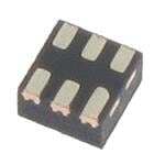
| 供应商器件封装 | 6-WSON(1.5x1.5) |
| 其它名称 | 296-28766-6 |
| 包装 | Digi-Reel® |
| 商标 | Texas Instruments |
| 安装类型 | 表面贴装 |
| 安装风格 | SMD/SMT |
| 封装 | Reel |
| 封装/外壳 | 6-WFDFN |
| 封装/箱体 | WSON-6 |
| 工作温度 | -40°C ~ 125°C |
| 工厂包装数量 | 250 |
| 最大工作温度 | + 125 C |
| 最大输入电压 | 5.5 V |
| 最小工作温度 | - 40 C |
| 标准包装 | 1 |
| 电压-跌落(典型值) | 0.14V @ 200mA |
| 电压-输入 | 2 V ~ 5.5 V |
| 电压-输出 | 3.3V |
| 电流-输出 | 200mA |
| 电流-限制(最小值) | 220mA |
| 稳压器拓扑 | 正,固定式 |
| 稳压器数 | 2 |
| 系列 | TLV7113333D |
| 输出电流 | 1.2 A |
| 输出类型 | Fixed |


PDF Datasheet 数据手册内容提取
TLV710 Series TLV711 Series www.ti.com SBVS142A–JULY2010–REVISEDAUGUST2010 Dual, 200mA, Low-I Q Low-Dropout Regulator for Portable Devices FEATURES DESCRIPTION 1 • VeryLowDropout: The TLV710 and TLV711 series of dual, low-dropout 2 – 150mVatI =200mAandV =2.8V (LDO) linear regulators are low quiescent current OUT OUT devices with excellent line and load transient – 75mVatI =100mAandV =2.8V OUT OUT performance. These LDOs are designed for – 40mVatI =50mAandV =2.8V OUT OUT power-sensitive applications. These devices provide • 2%AccuracyOverTemperature atypicalaccuracyof2%overtemperature. • LowIQof35mAperRegulator The TLV711 series provides an active pulldown • MultipleFixedOutputVoltageCombinations circuittoquicklydischargetheoutputs. Possiblefrom1.2Vto4.8V In addition, the TLV711-D series of devices have • HighPSRR:70dBat1kHz pull-down resistors at the EN pins. This design helps • StablewithEffectiveCapacitanceof0.1mF(1) in disabling the device when the signal-driving EN pins are in a weak, indeterminate state (for example, • Over-CurrentandThermalProtection the GPIO of a processor that might be three-stated • DedicatedVREFforEachOutputMinimizes during startup). The pull-down resistor pulls the Crosstalk voltage to the EN pins down to 0V, thus disabling the • Availablein1.5mm×1.5mmSON-6Package device. (1) SeetheInputandOutputCapacitorRequirementsinthe The TLV710 and TLV711 series are available in a ApplicationInformationsection 1.5mm x 1.5mm SON-6 package, and are ideal for handheldapplications. APPLICATIONS • WirelessHandsets,SmartPhones,PDAs • MP3PlayersandOtherHandheldProducts TLV710 TLV711 1.5mm x 1.5mm SON-6 (TOP VIEW) EN1 1 6 OUT1 IN 2 5 OUT2 EN2 3 4 GND TypicalApplicationCircuit VIN IN OUT1 VOUT1 EN1 OUT2 V OUT2 C ON OUT1 CIN COUT2 1mF OFF ON EN2 GND 1CmeFramic Ceramic OFF 1 Pleasebeawarethatanimportantnoticeconcerningavailability,standardwarranty,anduseincriticalapplicationsofTexas Instrumentssemiconductorproductsanddisclaimerstheretoappearsattheendofthisdatasheet. Alltrademarksarethepropertyoftheirrespectiveowners. 2 PRODUCTIONDATAinformationiscurrentasofpublicationdate. Copyright©2010,TexasInstrumentsIncorporated Products conform to specifications per the terms of the Texas Instruments standard warranty. Production processing does not necessarilyincludetestingofallparameters.
TLV710 Series TLV711 Series SBVS142A–JULY2010–REVISEDAUGUST2010 www.ti.com This integrated circuit can be damaged by ESD. Texas Instruments recommends that all integrated circuits be handled with appropriateprecautions.Failuretoobserveproperhandlingandinstallationprocedurescancausedamage. ESDdamagecanrangefromsubtleperformancedegradationtocompletedevicefailure.Precisionintegratedcircuitsmaybemore susceptibletodamagebecauseverysmallparametricchangescouldcausethedevicenottomeetitspublishedspecifications. ORDERINGINFORMATION(1) PRODUCT V (2) OUT TLV710xxyyqwwwz XXisnominaloutputvoltageofchannel1(forexample18=1.8V). TLV711xxyyqwwwz YYisnominaloutputvoltageofchannel2(forexample28=2.8V). Qisoptional.Use"U"fordeviceswithENpinpull-upresistor,and"D"fordeviceswithENpinpull-downresistor. WWWispackagedesignator. Zispackagequantity.Use"R"forreel(3000pieces),and"T"fortape(250pieces). (1) ForthemostcurrentpackageandorderinginformationseethePackageOptionAddendumattheendofthisdocument,orvisitthe deviceproductfolderonwww.ti.com. (2) Outputvoltagesfrom1.2Vto4.8Vin50mVincrementsareavailablethroughtheuseofinnovativefactoryOTPprogramming;minimum orderquantitiesmayapply.Contactfactoryfordetailsandavailability. ABSOLUTE MAXIMUM RATINGS(1) AtT =–40°Cto+125°C(unlessotherwisenoted). J VALUE MIN MAX UNIT IN –0.3 +6.0 V Voltage(2) EN –0.3 V +0.3 V IN OUT –0.3 +6.0 V Current OUT Internallylimited A Outputshort-circuitduration Indefinite s Operatingjunction,T –55 +150 °C J Temperature Storage,T –55 +150 °C stg Humanbodymodel(HBM)QSS009-105(JESD22-A114A) 2 kV ElectrostaticDischargeRating Chargeddevicemodel(CDM)QSS009-147 500 V (JESD22-C101B.01) (1) StressesbeyondthoselistedunderAbsoluteMaximumRatingsmaycausepermanentdamagetothedevice.Thesearestressratings only,andfunctionaloperationofthedeviceattheseoranyotherconditionsbeyondthoseindicatedisnotimplied.Exposureto absolute-maximum-ratedconditionsforextendedperiodsmyaffectdevicereliability. (2) Allvoltageswithrespecttoground. THERMAL INFORMATION(1) TLV710,TLV711 THERMALMETRIC(2) DSE UNITS 6PINS y Junction-to-topcharacterizationparameter 6 °C/W JT (1) SeethePowerDissipationsectionformoredetails. (2) Formoreinformationabouttraditionalandnewthermalmetrics,seetheICPackageThermalMetricsapplicationreport,SPRA953. 2 SubmitDocumentationFeedback Copyright©2010,TexasInstrumentsIncorporated
TLV710 Series TLV711 Series www.ti.com SBVS142A–JULY2010–REVISEDAUGUST2010 ELECTRICAL CHARACTERISTICS AtT =+25°C,V =V +0.5Vor2.0V(whicheverisgreater),I =10mA,V =V =0.9V,andC =C = J IN OUT(TYP) OUT EN1 EN2 OUT1 OUT2 1mF,unlessotherwisenoted. TLV710,TLV711 PARAMETER TESTCONDITIONS MIN TYP MAX UNIT VIN Inputvoltagerange 2.0 5.5 V VO Outputvoltagerange 1.2 4.8 V VOUT DCoutputaccuracy –40°C≤TJ≤+125°C –2 +2 % ΔVO/ΔVIN Lineregulation VOUT(NOM)+0.5V≤VIN≤5.5V 1 5 mV ΔVO/ΔIOUT Loadregulation 0mA≤IOUT≤200mA 5 15 mV VIN=0.98V×VOUT(NOM),IOUT=200mA, 200 285 mV 2V≤VOUT<2.4V VIN=0.98V×VOUT(NOM),IOUT=200mA, 175 250 mV 2.4V≤VOUT<2.8V VDO Dropoutvoltage VIN=0.98V×VOUT(NOM),IOUT=200mA, 150 215 mV 2.8V≤VOUT<3.3V VIN=0.98V×VOUT(NOM),IOUT=200mA, 140 200 mV 3.3V≤VOUT≤4.8V ICL Outputcurrentlimit VOUT=0.9V×VOUT(NOM) 220 350 550 mA VEN1=high,VEN2=low,IOUT1=0mA 35 mA IQ Quiescentcurrent VEN1=low,VEN2=high,IOUT2=0mA 35 mA VEN1=high,VEN2=high,IOUT=0mA 70 110 µA IGND Groundpincurrent IOUT1=IOUT2=200mA 360 µA ISHUTDOWN Shutdowncurrent VEN1,2≤0.4V,2.0V≤VIN≤4.5V 2.5 4 mA f=10Hz 80 dB f=100Hz 75 dB PSRR Power-supplyrejectionratio VOUT=1.8V f=1kHz 70 dB f=10kHz 70 dB f=100kHz 50 dB VN Outputnoisevoltage BW=100Hzto100kHz,VOUT=1.8V 48 mVRMS tSTR Startuptime(1) COUT=1.0mF,IOUT=200mA 100 ms VHI Enablehigh(enabled) 0.9 VIN V VLO Enablelow(shutdown) 0 0.4 V TLV710,TLV711 0.04 mA IEN Enablepincurrent,enabled TLV710-D,TLV711-D 6 mA UVLO Undervoltagelockout VINrising 1.9 V TJ Operatingjunctiontemperature –40 +125 °C Shutdown,temperatureincreasing +165 °C TSD Thermalshutdowntemperature Reset,temperaturedecreasing +145 °C (1) Startuptime=timefromENassertionto0.98xV . OUT(NOM) Copyright©2010,TexasInstrumentsIncorporated SubmitDocumentationFeedback 3
TLV710 Series TLV711 Series SBVS142A–JULY2010–REVISEDAUGUST2010 www.ti.com FUNCTIONAL BLOCK DIAGRAM TLV711 and TLV711-D only 120W Bandgap TLV710-D and TLV711-D only UVLO Current Limit Thermal Shutdown OUT1 Enable EN1 and Power EN2 Control Logic OUT2 150kW Thermal Shutdown Current IN Limit UVLO TLV710-D and TLV711-D only Bandgap 120W TLV711 and TLV711-D only GND 4 SubmitDocumentationFeedback Copyright©2010,TexasInstrumentsIncorporated
TLV710 Series TLV711 Series www.ti.com SBVS142A–JULY2010–REVISEDAUGUST2010 PIN CONFIGURATION DSEPACKAGE 1.5mmx1.5mmSON-6 (TOPVIEW) EN1 1 6 OUT1 IN 2 5 OUT2 EN2 3 4 GND PINDESCRIPTIONS NAME PINNO. DESCRIPTION Enablepinforregulator1.DrivingEN1over0.9Vturnsonregulator1.DrivingENbelow0.4Vputsregulator EN1 1 1intoshutdownmode. Inputpin.Asmallcapacitorisneededfromthispintogroundtoassurestability.SeeInputandOutput IN 2 CapacitorRequirementsintheApplicationInformationsectionformoredetails. Enablepinforregulator2.DrivingEN2over0.9Vturnsonregulator2.DrivingEN2below0.4Vputs EN2 3 regulator2intoshutdownmode. GND 4 Groundpin. Regulatedoutputvoltagepin.Asmall1mFceramiccapacitorisneededfromthispintogroundtoassure OUT2 5 stability.SeeInputandOutputCapacitorRequirementsintheApplicationInformationsectionformore details. Regulatedoutputvoltagepin.Asmall1mFceramiccapacitorisneededfromthispintogroundtoassure OUT1 6 stability.SeeInputandOutputCapacitorRequirementsintheApplicationInformationsectionformore details. Copyright©2010,TexasInstrumentsIncorporated SubmitDocumentationFeedback 5
TLV710 Series TLV711 Series SBVS142A–JULY2010–REVISEDAUGUST2010 www.ti.com TYPICAL CHARACTERISTICS OveroperatingtemperaturerangeofT =–40°Cto+125°C,V =V =V ,C =1mF,C =1mF,andC =1mF,unlessotherwise J EN1 EN2 IN IN OUT1 OUT2 noted.TypicalvaluesareatT =+25°C. J LINEREGULATION:V LINEREGULATION:V OUT1 OUT2 (TLV7101828) (TLV7101828) 1.90 2.90 I = 10mA I = 10mA 1.88 OUT1 2.88 OUT1 I = 10mA I = 10mA OUT2 OUT2 1.86 2.86 1.84 2.84 1.82 2.82 V) V) (UT 1.80 (UT 2.80 O O V 1.78 V 2.78 1.76 +125°C 2.76 +125°C 1.74 +85°C 2.74 +85°C +25°C +25°C 1.72 2.72 -40°C -40°C 1.70 2.70 2.1 2.6 3.1 3.6 4.1 4.6 5.1 5.6 3.1 3.6 4.1 4.6 5.1 5.6 V (V) V (V) IN IN Figure1. Figure2. LINEREGULATION:V LINEREGULATION:V OUT1 OUT2 (TLV7101828) (TLV7101828) 1.90 2.90 I = 200mA I = 0mA 1.88 OUT1 2.88 OUT1 I = 0mA I = 200mA OUT2 OUT2 1.86 2.86 1.84 2.84 1.82 2.82 V) V) (UT 1.80 (UT 2.80 O O V 1.78 V 2.78 1.76 +125°C 2.76 +125°C 1.74 +85°C 2.74 +85°C +25°C +25°C 1.72 2.72 -40°C -40°C 1.70 2.70 2.1 2.6 3.1 3.6 4.1 4.6 5.1 5.6 3.1 3.6 4.1 4.6 5.1 5.6 V (V) V (V) IN IN Figure3. Figure4. LINEREGULATION:V LINEREGULATION:V OUT1 OUT2 (TLV7103333) (TLV7103333) 3.40 3.40 I = 10mA I = 10mA 3.38 OUT1 3.38 OUT1 I = 10mA I = 10mA OUT2 OUT2 3.36 3.36 3.34 3.34 3.32 3.32 V) V) (UT 3.30 (UT 3.30 O O V 3.28 V 3.28 3.26 +125°C 3.26 +125°C 3.24 +85°C 3.24 +85°C +25°C +25°C 3.22 3.22 -40°C -40°C 3.20 3.20 3.6 3.8 4.0 4.2 4.4 4.6 4.8 5.0 5.2 5.4 5.6 3.6 3.8 4.0 4.2 4.4 4.6 4.8 5.0 5.2 5.4 5.6 V (V) V (V) IN IN Figure5. Figure6. 6 SubmitDocumentationFeedback Copyright©2010,TexasInstrumentsIncorporated
TLV710 Series TLV711 Series www.ti.com SBVS142A–JULY2010–REVISEDAUGUST2010 TYPICAL CHARACTERISTICS (continued) OveroperatingtemperaturerangeofT =–40°Cto+125°C,V =V =V ,C =1mF,C =1mF,andC =1mF, J EN1 EN2 IN IN OUT1 OUT2 unlessotherwisenoted.TypicalvaluesareatT =+25°C. J LINEREGULATION:V LINEREGULATION:V OUT1 OUT2 (TLV7103333) (TLV7103333) 3.40 3.40 I = 200mA I = 0mA 3.38 OUIT1 = 0mA 3.38 I OU=T1200mA OUT2 OUT2 3.36 3.36 3.34 3.34 3.32 3.32 V) V) (UT 3.30 (UT 3.30 O O V 3.28 V 3.28 3.26 +125°C 3.26 +125°C 3.24 +85°C 3.24 +85°C +25°C +25°C 3.22 3.22 -40°C -40°C 3.20 3.20 3.6 3.8 4.0 4.2 4.4 4.6 4.8 5.0 5.2 5.4 5.6 3.6 3.8 4.0 4.2 4.4 4.6 4.8 5.0 5.2 5.4 5.6 V (V) V (V) IN IN Figure7. Figure8. LINEREGULATION:V LINEREGULATION:V OUT1 OUT2 (TLV7111525) (TLV7111525) 1.60 2.60 I = 10mA I = 10mA 1.58 OUT1 2.58 OUT1 I = 10mA I = 10mA OUT2 OUT2 1.56 2.56 1.54 2.54 1.52 2.52 V) V) (UT 1.50 (UT 2.50 O O V 1.48 V 2.48 1.46 +125°C 2.46 +125°C 1.44 +85°C 2.44 +85°C +25°C +25°C 1.42 2.42 -40°C -40°C 1.40 2.40 2.0 2.5 3.0 3.5 4.0 4.5 5.0 5.5 3.0 3.5 4.0 4.5 5.0 5.5 V (V) V (V) IN IN Figure9. Figure10. LINEREGULATION:V LINEREGULATION:V OUT1 OUT2 (TLV7111525) (TLV7111525) 1.60 2.60 I = 200mA I = 0mA 1.58 OUT1 2.58 OUT1 I = 0mA OUT2 1.56 2.56 1.54 2.54 1.52 2.52 V) V) (UT 1.50 (UT 2.50 O O V 1.48 V 2.48 1.46 +125°C 2.46 +125°C 1.44 +85°C 2.44 +85°C +25°C +25°C 1.42 2.42 -40°C -40°C 1.40 2.40 2.0 2.5 3.0 3.5 4.0 4.5 5.0 5.5 3.0 3.5 4.0 4.5 5.0 5.5 V (V) V (V) IN IN Figure11. Figure12. Copyright©2010,TexasInstrumentsIncorporated SubmitDocumentationFeedback 7
TLV710 Series TLV711 Series SBVS142A–JULY2010–REVISEDAUGUST2010 www.ti.com TYPICAL CHARACTERISTICS (continued) OveroperatingtemperaturerangeofT =–40°Cto+125°C,V =V =V ,C =1mF,C =1mF,andC =1mF, J EN1 EN2 IN IN OUT1 OUT2 unlessotherwisenoted.TypicalvaluesareatT =+25°C. J LOADREGULATION:V LOADREGULATION:V OUT1 OUT2 (TLV7101828) (TLV7101828) 1.90 2.90 V = 3.3V V = 3.3V 1.88 IN 2.88 IN 1.86 2.86 1.84 2.84 1.82 2.82 V) V) (UT 1.80 (UT 2.80 O O V 1.78 V 2.78 1.76 +125°C 2.76 +125°C 1.74 +85°C 2.74 +85°C +25°C +25°C 1.72 2.72 -40°C -40°C 1.70 2.70 0 20 40 60 80 100 120 140 160 180 200 0 20 40 60 80 100 120 140 160 180 200 I (mA) I (mA) OUT OUT Figure13. Figure14. LOADREGULATION:V LOADREGULATION:V OUT1 OUT2 (TLV7103333) (TLV7103333) 3.40 3.40 V = 3.8V V = 3.8V 3.38 IN 3.38 IN 3.36 3.36 3.34 3.34 3.32 3.32 V) V) (UT 3.30 (UT 3.30 O O V 3.28 V 3.28 3.26 +125°C 3.26 +125°C 3.24 +85°C 3.24 +85°C +25°C +25°C 3.22 3.22 -40°C -40°C 3.20 3.20 0 20 40 60 80 100 120 140 160 180 200 0 20 40 60 80 100 120 140 160 180 200 I (mA) I (mA) OUT OUT Figure15. Figure16. LOADREGULATION:V LOADREGULATION:V OUT1 OUT2 (TLV7111525) (TLV7111525) 1.60 2.60 V = 3.0V V = 3.0V 1.58 IN 2.58 IN 1.56 2.56 1.54 2.54 1.52 2.52 V) V) (UT 1.50 (UT 2.50 O O V 1.48 V 2.48 1.46 +125°C 2.46 +125°C 1.44 +85°C 2.44 +85°C +25°C +25°C 1.42 2.42 -40°C -40°C 1.40 2.40 0 20 40 60 80 100 120 140 160 180 200 0 20 40 60 80 100 120 140 160 180 200 I (mA) I (mA) OUT OUT Figure17. Figure18. 8 SubmitDocumentationFeedback Copyright©2010,TexasInstrumentsIncorporated
TLV710 Series TLV711 Series www.ti.com SBVS142A–JULY2010–REVISEDAUGUST2010 TYPICAL CHARACTERISTICS (continued) OveroperatingtemperaturerangeofT =–40°Cto+125°C,V =V =V ,C =1mF,C =1mF,andC =1mF, J EN1 EN2 IN IN OUT1 OUT2 unlessotherwisenoted.TypicalvaluesareatT =+25°C. J DROPOUTVOLTAGE DROPOUTVOLTAGE vsINPUTVOLTAGE vsINPUTVOLTAGE 70 120 V = V = 4.8V V = V = 4.8V OUT1 OUT2 OUT1 OUT2 60 IOUT= 50mA 100 IOUT= 100mA 50 80 V) 40 V) m m ( ( 60 DO 30 DO V V 40 20 +125°C +125°C +85°C +85°C 10 +25°C 20 +25°C -40°C -40°C 0 0 2.0 2.4 2.8 3.2 3.6 4.0 4.4 4.8 2.0 2.4 2.8 3.2 3.6 4.0 4.4 4.8 V (V) V (V) IN IN Figure19. Figure20. DROPOUTVOLTAGE DROPOUTVOLTAGE vsINPUTVOLTAGE vsINPUTVOLTAGE 180 250 V = V = 4.8V V = V = 4.8V 160 OUT1 OUT2 OUT1 OUT2 I = 150mA I = 200mA OUT OUT 140 200 120 V) 100 V) 150 m m ( ( O 80 O VD VD 100 60 +125°C +125°C 40 +85°C 50 +85°C 20 +25°C +25°C -40°C -40°C 0 0 2.0 2.4 2.8 3.2 3.6 4.0 4.4 4.8 2.0 2.4 2.8 3.2 3.6 4.0 4.4 4.8 V (V) V (V) IN IN Figure21. Figure22. DROPOUTVOLTAGEvsOUTPUTCURRENT:V DROPOUTVOLTAGEvsOUTPUTCURRENT:V /V OUT2 OUT1 OUT2 (TLV7101828) (TLV7103333) 200 180 180 160 160 140 140 120 V) 120 V) 100 m m ( 100 ( O O 80 VD 80 VD 60 60 +125°C +125°C 40 +85°C 40 +85°C 20 +25°C 20 +25°C -40°C -40°C 0 0 0 20 40 60 80 100 120 140 160 180 200 0 20 40 60 80 100 120 140 160 180 200 I (mA) I (mA) OUT OUT Figure23. Figure24. Copyright©2010,TexasInstrumentsIncorporated SubmitDocumentationFeedback 9
TLV710 Series TLV711 Series SBVS142A–JULY2010–REVISEDAUGUST2010 www.ti.com TYPICAL CHARACTERISTICS (continued) OveroperatingtemperaturerangeofT =–40°Cto+125°C,V =V =V ,C =1mF,C =1mF,andC =1mF, J EN1 EN2 IN IN OUT1 OUT2 unlessotherwisenoted.TypicalvaluesareatT =+25°C. J DROPOUTVOLTAGEvsOUTPUTCURRENT:V OUTPUTVOLTAGEvsTEMPERATURE:V OUT2 OUT1 (TLV7111525) (TLV7101828) 250 1.90 V = 3.3V 1.88 IN 200 1.86 1.84 V(mV)DO 115000 V(V)OUT 111...887208 +125°C 1.76 50 +85°C 1.74 10mA +25°C 150mA 1.72 -40°C 200mA 0 1.70 0 20 40 60 80 100 120 140 160 180 200 -40 -25 -10 5 20 35 50 65 80 95 110 125 IOUT(mA) Junction Temperature (°C) Figure25. Figure26. OUTPUTVOLTAGEvsTEMPERATURE:V OUTPUTVOLTAGEvsTEMPERATURE:V OUT2 OUT1 (TLV7101828) (TLV7103333) 2.90 3.40 V = 3.3V V = 3.8V 2.88 IN 3.38 IN 2.86 3.36 2.84 3.34 2.82 3.32 V) V) (UT 2.80 (UT 3.30 O O V 2.78 V 3.28 2.76 3.26 2.74 10mA 3.24 10mA 150mA 150mA 2.72 3.22 200mA 200mA 2.70 3.20 -40 -25 -10 5 20 35 50 65 80 95 110 125 -40 -25 -10 5 20 35 50 65 80 95 110 125 Junction Temperature (°C) Junction Temperature (°C) Figure27. Figure28. OUTPUTVOLTAGEvsTEMPERATURE:V OUTPUTVOLTAGEvsTEMPERATURE:V OUT2 OUT1 (TLV7103333) (TLV7111525) 3.40 1.60 V = 3.8V V = 3.0V 3.38 IN 1.58 IN 3.36 1.56 3.34 1.54 3.32 1.52 V) V) (UT 3.30 (UT 1.50 O O V 3.28 V 1.48 3.26 1.46 3.24 10mA 1.44 10mA 150mA 150mA 3.22 1.42 200mA 200mA 3.20 1.40 -40 -25 -10 5 20 35 50 65 80 95 110 125 -40 -25 -10 5 20 35 50 65 80 95 110 125 Junction Temperature (°C) Junction Temperature (°C) Figure29. Figure30. 10 SubmitDocumentationFeedback Copyright©2010,TexasInstrumentsIncorporated
TLV710 Series TLV711 Series www.ti.com SBVS142A–JULY2010–REVISEDAUGUST2010 TYPICAL CHARACTERISTICS (continued) OveroperatingtemperaturerangeofT =–40°Cto+125°C,V =V =V ,C =1mF,C =1mF,andC =1mF, J EN1 EN2 IN IN OUT1 OUT2 unlessotherwisenoted.TypicalvaluesareatT =+25°C. J OUTPUTVOLTAGEvsTEMPERATURE:V GROUNDPINCURRENTvsINPUTVOLTAGE:I OUT2 Q1 (TLV7111525) (TLV7101828) 2.60 50 2.58 V = 3.0V 45 VIN= 3.3V IN 2.56 40 2.54 35 V) 2.52 A) 30 (UT 2.50 (mD 25 O N V 2.48 G 20 I 2.46 15 +125°C 2.44 10mA 10 +85°C 150mA +25°C 2.42 5 200mA -40°C 2.40 0 -40 -25 -10 5 20 35 50 65 80 95 110 125 2.1 2.6 3.1 3.6 4.1 4.6 5.1 5.6 Junction Temperature (°C) VIN(V) Figure31. Figure32. GROUNDPINCURRENTvsINPUTVOLTAGE:I GROUNDPINCURRENTvsINPUTVOLTAGE:I Q2 Q1 (TLV7101828) (TLV7103333) 50 50 45 45 40 40 35 35 30 30 A) A) (m 25 (m 25 D D N N G 20 G 20 I I 15 +125°C 15 +125°C 10 +85°C 10 +85°C +25°C +25°C 5 5 -40°C -40°C 0 0 3.1 3.6 4.1 4.6 5.1 5.6 3.6 4.0 4.4 4.8 5.2 5.6 V (V) V (V) IN IN Figure33. Figure34. GROUNDPINCURRENTvsINPUTVOLTAGE:I GROUNDPINCURRENTvsINPUTVOLTAGE:I Q2 Q1 (TLV7103333) (TLV7111525) 50 50 45 45 40 40 35 35 30 30 A) A) (m 25 (m 25 D D N N G 20 G 20 I I 15 +125°C 15 +125°C 10 +85°C 10 +85°C +25°C +25°C 5 5 -40°C -40°C 0 0 3.6 4.0 4.4 4.8 5.2 5.6 2.1 2.6 3.1 3.6 4.1 4.6 5.1 5.6 V (V) V (V) IN IN Figure35. Figure36. Copyright©2010,TexasInstrumentsIncorporated SubmitDocumentationFeedback 11
TLV710 Series TLV711 Series SBVS142A–JULY2010–REVISEDAUGUST2010 www.ti.com TYPICAL CHARACTERISTICS (continued) OveroperatingtemperaturerangeofT =–40°Cto+125°C,V =V =V ,C =1mF,C =1mF,andC =1mF, J EN1 EN2 IN IN OUT1 OUT2 unlessotherwisenoted.TypicalvaluesareatT =+25°C. J GROUNDPINCURRENTvsINPUTVOLTAGE:I GROUNDPINCURRENTvsLOAD:I Q2 Q1 (TLV7111525) (TLV7101828) 50 350 V = 3.3V 45 IN 300 40 35 250 30 A) A) 200 (m 25 (m D D N N 150 G 20 G I I 15 +125°C 100 +125°C 10 +85°C +85°C +25°C 50 +25°C 5 -40°C -40°C 0 0 2.8 3.2 3.6 4.0 4.4 4.8 5.2 5.6 0 20 40 60 80 100 120 140 160 180 200 V (V) I (mA) IN OUT Figure37. Figure38. GROUNDPINCURRENTvsLOAD:I GROUNDPINCURRENTvsLOAD:I Q2 Q1 (TLV7103333) (TLV7111525) 350 350 V = 3.8V V = 3.0V IN IN 300 300 250 250 A) 200 A) 200 m m ( ( D D N 150 N 150 G G I I 100 +125°C 100 +125°C +85°C +85°C 50 +25°C 50 +25°C -40°C -40°C 0 0 0 20 40 60 80 100 120 140 160 180 200 0 20 40 60 80 100 120 140 160 180 200 I (mA) I (mA) OUT OUT Figure39. Figure40. SHUTDOWNCURRENTvsINPUTVOLTAGE SHUTDOWNCURRENTvsINPUTVOLTAGE (TLV7101828) (TLV7103333) 4.0 4.0 3.5 3.5 3.0 3.0 2.5 2.5 A) A) m m ( 2.0 ( 2.0 N N D D H H IS 1.5 IS 1.5 1.0 +125°C 1.0 +125°C +85°C +85°C 5 +25°C 5 +25°C -40°C -40°C 0 0 2.0 2.5 3.0 3.5 4.0 4.5 5.0 5.5 2.0 2.5 3.0 3.5 4.0 4.5 5.0 5.5 V (V) V (V) IN IN Figure41. Figure42. 12 SubmitDocumentationFeedback Copyright©2010,TexasInstrumentsIncorporated
TLV710 Series TLV711 Series www.ti.com SBVS142A–JULY2010–REVISEDAUGUST2010 TYPICAL CHARACTERISTICS (continued) OveroperatingtemperaturerangeofT =–40°Cto+125°C,V =V =V ,C =1mF,C =1mF,andC =1mF, J EN1 EN2 IN IN OUT1 OUT2 unlessotherwisenoted.TypicalvaluesareatT =+25°C. J SHUTDOWNCURRENTvsINPUTVOLTAGE CURRENTLIMITvsINPUTVOLTAGE:I CL1 (TLV7111525) (TLV7101828) 4.0 500 +125°C 480 3.5 +85°C 460 +25°C 3.0 440 -40°C 2.5 (A)m 2.0 mA) 442000 N ( D M ISH 1.5 ILI 380 1.0 +125°C 360 +85°C 340 5 +25°C 320 -40°C 0 300 2.0 2.5 3.0 3.5 4.0 4.5 5.0 5.5 2.1 2.6 3.1 3.6 4.1 4.6 5.1 5.6 V (V) V (V) IN IN Figure43. Figure44. CURRENTLIMITvsINPUTVOLTAGE:I CURRENTLIMITvsINPUTVOLTAGE:I CL2 CL1 (TLV7101828) (TLV7103333) 500 500 +125°C +125°C 480 480 +85°C +85°C 460 +25°C 460 +25°C 440 -40°C 440 -40°C 420 420 A) A) m 400 m 400 ( ( M M ILI 380 ILI 380 360 360 340 340 320 320 300 300 3.1 3.6 4.1 4.6 5.1 5.6 3.6 4.0 4.4 4.8 5.2 5.6 V (V) V (V) IN IN Figure45. Figure46. CURRENTLIMITvsINPUTVOLTAGE:I CURRENTLIMITvsINPUTVOLTAGE:I CL2 CL1 (TLV7103333) (TLV7111525) 500 500 +125°C +125°C 480 480 +85°C +85°C 460 +25°C 460 +25°C 440 -40°C 440 -40°C 420 420 A) A) m 400 m 400 ( ( M M ILI 380 ILI 380 360 360 340 340 320 320 300 300 3.6 4.0 4.4 4.8 5.2 5.6 2.8 3.1 3.4 3.7 4.0 4.3 4.6 4.9 5.2 5.5 V (V) V (V) IN IN Figure47. Figure48. Copyright©2010,TexasInstrumentsIncorporated SubmitDocumentationFeedback 13
TLV710 Series TLV711 Series SBVS142A–JULY2010–REVISEDAUGUST2010 www.ti.com TYPICAL CHARACTERISTICS (continued) OveroperatingtemperaturerangeofT =–40°Cto+125°C,V =V =V ,C =1mF,C =1mF,andC =1mF, J EN1 EN2 IN IN OUT1 OUT2 unlessotherwisenoted.TypicalvaluesareatT =+25°C. J CURRENTLIMITvsINPUTVOLTAGE:I CL2 (TLV7111525) 500 +125°C 480 +85°C 460 +25°C 440 -40°C 420 A) m 400 ( M ILI 380 360 340 320 300 2.8 3.1 3.4 3.7 4.0 4.3 4.6 4.9 5.2 5.5 V (V) IN Figure49. POWER-SUPPLYRIPPLEREJECTIONvsFREQUENCY POWER-SUPPLYRIPPLEREJECTIONvsFREQUENCY (TLV7101828) (TLV7103333) 100 100 I = 30mA I = 30mA I = 30mA 9800 IOUT2= 30mA OVUTV1IN== 32..38VV 8900 OUT2 OVUTV1IN== 33..83VV OUT OUT 70 70 R (dB) 6500 IOUT2= 150mA R (dB) 6500 IOUT2= 150mA R R S 40 S 40 P P 30 30 20 20 10 10 0 0 10 100 1k 10k 100k 1M 10M 10 100 1k 10k 100k 1M 10M Frequency (Hz) Frequency (Hz) Figure50. Figure51. POWER-SUPPLYRIPPLEREJECTIONvsFREQUENCY OUTPUTSPECTRALNOISEDENSITY (TLV7111525) vsFREQUENCY(TLV7101828) 100 10 B) 98760000 IOIOUUT2T2== 3 105m0AmA IOVUOTVU1INT=== 3 320..m05AVV Density (V/Hz)mÖ 1 IVOOUTVU2TIN2=== 3 320..m38AVV PSRR (d 5400 al Noise 0.1 30 ctr e 0.01 20 Sp ut 10 p ut 0 O 0.001 10 100 1k 10k 100k 1M 10M 10 100 1k 10k 100k 1M 10M Frequency (Hz) Frequency (Hz) Figure52. Figure53. 14 SubmitDocumentationFeedback Copyright©2010,TexasInstrumentsIncorporated
TLV710 Series TLV711 Series www.ti.com SBVS142A–JULY2010–REVISEDAUGUST2010 TYPICAL CHARACTERISTICS (continued) OveroperatingtemperaturerangeofT =–40°Cto+125°C,V =V =V ,C =1mF,C =1mF,andC =1mF, J EN1 EN2 IN IN OUT1 OUT2 unlessotherwisenoted.TypicalvaluesareatT =+25°C. J OUTPUTSPECTRALNOISEDENSITY OUTPUTSPECTRALNOISEDENSITY vsFREQUENCY(TLV7103333) vsFREQUENCY(TLV7111525) 10 10 )Hz VIN= 3.8V Hz) VIN= 3.0V y (V/mÖ 1 IVOOUTU2T2== 3 30.m3AV y (V/mÖ 1 IVOOUTU1T1== 3 10.m5AV sit sit n n e e D D se 0.1 se 0.1 oi oi N N al al ctr ctr e 0.01 e 0.01 p p S S ut ut p p ut ut O 0.001 O 0.001 10 100 1k 10k 100k 1M 10M 10 100 1k 10k 100k 1M 10M Frequency (Hz) Frequency (Hz) Figure54. Figure55. LINETRANSIENTRESPONSE LINETRANSIENTRESPONSE V =1.2V,V =1.2V V =1.2V,V =1.2V OUT1 OUT2 OUT1 OUT2 3.0V Slew Rate = 1V/ms 5.5V Slew Rate = 1V/ms 1V/div IOUT= 30mA IOUT= 30mA 2.0V V 2V/div 2.0V V IN IN 5mV/div VOUT1 5mV/div VOUT1 5mV/div VOUT2 5mV/div VOUT2 Time (200ms/div) Time (200ms/div) Figure56. Figure57. LINETRANSIENTRESPONSE LINETRANSIENTRESPONSE V =1.8V,V =2.8V V =1.8V,V =2.8V OUT1 OUT2 OUT1 OUT2 Slew Rate = 1V/ms 5.5V Slew Rate = 1V/ms 4.3V IOUT= 30mA IOUT= 30mA 1V/div 3.3V VIN 1V/div 3.3V VIN 5mV/div VOUT1 5mV/div VOUT1 5mV/div VOUT2 5mV/div VOUT2 Time (200ms/div) Time (200ms/div) Figure58. Figure59. Copyright©2010,TexasInstrumentsIncorporated SubmitDocumentationFeedback 15
TLV710 Series TLV711 Series SBVS142A–JULY2010–REVISEDAUGUST2010 www.ti.com TYPICAL CHARACTERISTICS (continued) OveroperatingtemperaturerangeofT =–40°Cto+125°C,V =V =V ,C =1mF,C =1mF,andC =1mF, J EN1 EN2 IN IN OUT1 OUT2 unlessotherwisenoted.TypicalvaluesareatT =+25°C. J LINETRANSIENTRESPONSE V =4.8V,V =4.8V OUT1 OUT2 Slew Rate = 1V/ms I = 30mA 5.5V OUT 1V/div 5.3V V IN 5mV/div V OUT1 5mV/div V OUT2 Time (200ms/div) Figure60. LOADTRANSIENTRESPONSEANDCROSSTALK LOADTRANSIENTRESPONSEANDCROSSTALK V =1.2V,V =1.2V V =1.2V,V =1.2V OUT1 OUT2 OUT1 OUT2 200mA Slew Rate = 1V/ms Slew Rate = 1V/ms V = 2.0V 200mA V = 2.0V IN IN 100mA/div 0mA IOUT1 100mA/div 50mA IOUT1 50mV/div V 50mV/div V OUT1 OUT1 10mV/div VOUT2 10mV/div VOUT2 Time (50ms/div) Time (50ms/div) Figure61. Figure62. LOADTRANSIENTRESPONSEANDCROSSTALK LOADTRANSIENTRESPONSEANDCROSSTALK V =1.8V,V =2.8V V =1.8V,V =2.8V OUT1 OUT2 OUT1 OUT2 200mA Slew Rate = 1V/ms 200mA Slew Rate = 1V/ms VIN= 3.3V VIN= 3.3V 100mA/div 50mA I OUT2 100mA/div 0mA I OUT2 50mV/div V 20mV/div V OUT1 OUT2 V OUT2 50mV/div 5mV/div V OUT1 Time (50ms/div) Time (50ms/div) Figure63. Figure64. 16 SubmitDocumentationFeedback Copyright©2010,TexasInstrumentsIncorporated
TLV710 Series TLV711 Series www.ti.com SBVS142A–JULY2010–REVISEDAUGUST2010 TYPICAL CHARACTERISTICS (continued) OveroperatingtemperaturerangeofT =–40°Cto+125°C,V =V =V ,C =1mF,C =1mF,andC =1mF, J EN1 EN2 IN IN OUT1 OUT2 unlessotherwisenoted.TypicalvaluesareatT =+25°C. J LOADTRANSIENTRESPONSEANDCROSSTALK LOADTRANSIENTRESPONSEANDCROSSTALK V =4.8V,V =4.8V V =4.8V,V =4.8V OUT1 OUT2 OUT1 OUT2 Slew Rate = 1V/ms 200mA Slew Rate = 1V/ms 200mA VIN= 5.3V VIN= 5.3V 100mA/div 0mA I 50mA/div 50mA I OUT1 OUT1 V 50mV/div 50mV/div OUT1 V OUT1 5mV/div VOUT2 5mV/div VOUT2 Time (50ms/div) Time (50ms/div) Figure65. Figure66. V RAMPUP,RAMPDOWNRESPONSE V RAMPUP,RAMPDOWNRESPONSE IN IN V =1.2V,V =1.2V V =1.8V,V =2.8V OUT1 OUT2 OUT1 OUT2 I = 30mA I = 30mA OUT OUT V V V V IN/ EN IN/ EN 1V/div 1V/div VOUT2 V OUT1 V /V OUT1 OUT2 Time (200ms/div) Time (200ms/div) Figure67. Figure68. V RAMPUP,RAMPDOWNRESPONSE IN V =4.8V,V =4.8V OUT1 OUT2 I = 30mA OUT V V IN/ EN 1V/div VOUT1/VOUT2 Time (200ms/div) Figure69. Copyright©2010,TexasInstrumentsIncorporated SubmitDocumentationFeedback 17
TLV710 Series TLV711 Series SBVS142A–JULY2010–REVISEDAUGUST2010 www.ti.com APPLICATION INFORMATION The TLV710 and TLV711 series of devices belong to BOARD LAYOUT RECOMMENDATIONS TO a new family of next generation, value LDO IMPROVE PSRR AND NOISE PERFORMANCE regulators. These devices consume low quiescent current and deliver excellent line and load transient Input and output capacitors should be placed as performance. These features, combined with low close to the device pins as possible. To improve ac noise, very good PSRR with little (V to V ) performance such as PSRR, output noise, and IN OUT headroom, make these devices ideal for RF portable transient response, it is recommended that the board applications. This family of LDO regulators offers be designed with separate ground planes for V and IN current limit and thermal protection, and is specified V , with the ground plane connected only at the OUT from–40°Cto+125°C. GND pin of the device. In addition, the ground connection for the output capacitor should be INPUT AND OUTPUT CAPACITOR connected directly to the GND pin of the device. High REQUIREMENTS ESRcapacitorsmaydegradePSRR. 1.0mF X5R- and X7R-type ceramic capacitors are INTERNAL CURRENT LIMIT recommended because they have minimal variation in value and equivalent series resistance (ESR) over The TLV710 and TLV711 internal current limits help temperature. protect the regulator during fault conditions. During current limit, the output sources a fixed amount of However, the TLV710 and TLV711 are designed to current that is largely independent of output voltage. be stable with an effective capacitance of 0.1mF or In such a case, the output voltage is not regulated, larger at the output. Thus, the device would also be andisV =I ×R . stable with capacitors of other dielectrics, as long as OUT LIMIT LOAD the effective capacitance under operating bias The PMOS pass transistor dissipates (V – V ) × IN OUT voltage and temperature is greater than 0.1mF. This I until thermal shutdown is triggered and the LIMIT effective capacitance refers to the capacitance that device is turned off. As the device cools down, it is the device sees under operating bias voltage and turned on by the internal thermal shutdown circuit. If temperature conditions (that is, the capacitance after the fault condition continues, the device cycles taking bias voltage and temperature derating into between current limit and thermal shutdown. See the consideration.) Thermal Information section for more details. The PMOS pass element in the TLV710 and TLV711 has In addition to allowing the use of cost-effective a built-in body diode that conducts current when the dielectrics, these devices also enable using smaller voltage at OUT exceeds the voltage at IN. This footprint capacitors that have a higher derating in current is not limited, so if extended reverse voltage size-constrainedapplications. operation is anticipated, external limiting to 5% of Note that using a 0.1mF rating capacitor at the output ratedoutputcurrentisrecommended. of the LDO regulator does not ensure stability because the effective capacitance under operating SHUTDOWN conditions would be less than 0.1mF. The maximum The enable pin (EN) is active high. The device is ESRshouldbelessthan200mΩ. enabled when EN pin goes above 0.9V. This Although an input capacitor is not required for relatively lower value of voltage needed to turn the stability, it is good analog design practice to connect LDO regulator on can be used to enable the device a 0.1mF to 1.0mF low ESR capacitor across the IN with the GPIO of recent processors whose GPIO and GND pins of the regulator. This capacitor voltageislowerthantraditionalmicrocontrollers. counteracts reactive input sources and improves The device is turned off when the EN pin is held at transient response, noise rejection, and ripple less than 0.4V. When shutdown capability is not rejection. A higher-value capacitor may be necessary required,theENpincanconnectedtotheINpin. if large, fast-rise-time load transients are anticipated, or if the device is not located near the power source. The TLV711 has internal pull-down circuitry that If source impedance is more than 2Ω, a 0.1mF input dischargesoutputwithatimeconstantof: capacitormaybenecessarytoensurestability. 120 · R t= L · C 120 + R OUT L Where: R =loadresistance L C =outputcapacitor (1) OUT 18 SubmitDocumentationFeedback Copyright©2010,TexasInstrumentsIncorporated
TLV710 Series TLV711 Series www.ti.com SBVS142A–JULY2010–REVISEDAUGUST2010 DROPOUT VOLTAGE use worst-case loads and signal conditions. For good reliability, thermal protection should trigger at least The TLV710 and TLV711 use a PMOS pass +35°C above the maximum expected ambient transistor to achieve low dropout. When (V – V ) IN OUT condition of the particular application. This is less than the dropout voltage (V ), the PMOS DO configuration produces a worst-case junction pass device is in the linear region of operation and temperature of +125°C at the highest expected the input-to-output resistance is the R of the DS(ON) ambienttemperatureandworst-caseload. PMOS pass element. V scales approximately with DO the output current because the PMOS device The internal protection circuitry of the TLV710 and behavesasaresistorindropout. TLV711 has been designed to protect against overload conditions. It was not intended to replace As with any linear regulator, PSRR and transient proper heatsinking. Continuously running the response are degraded as (V – V ) approaches IN OUT TLV710/ TLV711 into thermal shutdown degrades dropout. devicereliability. TRANSIENT RESPONSE POWER DISSIPATION As with any regulator, increasing the size of the The ability to remove heat from a die is different for output capacitor reduces over/undershoot magnitude each package type, presenting different butincreasesdurationofthetransientresponse. considerations in the printed circuit board (PCB) The TLV710 and TLV711 each have a dedicated layout. The PCB area around the device that is free V . Consequently, crosstalk from one channel to of other components moves the heat from the device REF theotherasaresultoftransientsiscloseto0V. totheambientair. Performance data for the TLV710 evaluation module UNDERVOLTAGE LOCKOUT (UVLO) (EVM) are shown in Table 1. The EVM is a 2-layer The TLV710 and TLV711 use an undervoltage board with 2 ounces of copper per side. The lockout circuit to keep the output shut off until the dimension and layout are shown in Figure 70 and internalcircuitryisoperatingproperly. Figure 71. Using heavier copper increases the effectiveness of removing heat from the device. The THERMAL INFORMATION addition of plated through-holes in the heat-dissipating layer also improves the heatsink Thermal protection disables the output when the effectiveness. Power dissipation depends on input junction temperature rises to approximately +165°C, voltageandloadconditions. allowing the device to cool. When the junction temperature cools to approximately +145°C, the Power dissipation (PD) is equal to the product of the outputcircuitryisagainenabled.Dependingonpower output current and the voltage drop across the output dissipation, thermal resistance, and ambient passelement,asshowninEquation2: temperature, the thermal protection circuit may cycle P =(V –V )×I (2) D IN OUT OUT on and off. This cycling limits the dissipation of the regulator, protecting it from damage as a result of PACKAGE MOUNTING overheating. SolderpadfootprintrecommendationsfortheTLV710 Any tendency to activate the thermal protection circuit andTLV711areavailablefromtheTexasInstruments indicates excessive power dissipation or an Web site at www.ti.com. The recommended land inadequate heatsink. For reliable operation, junction pattern for the DSE (SON-6) package is shown in temperature should be limited to +125°C maximum. Figure72. Toestimatethemarginofsafetyinacompletedesign (including heatsink), increase the ambient temperature until the thermal protection is triggered; Table1.TLV710EVMDissipationRatings PACKAGE R T <+25°C T =+70°C T =+85°C qJA A A A DSE 170°C/W 585mW 320mW 235mW Copyright©2010,TexasInstrumentsIncorporated SubmitDocumentationFeedback 19
TLV710 Series TLV711 Series SBVS142A–JULY2010–REVISEDAUGUST2010 www.ti.com 33mm 27mm Figure70. TopLayer 33mm 27mm Figure71. BottomLayer 20 SubmitDocumentationFeedback Copyright©2010,TexasInstrumentsIncorporated
TLV710 Series TLV711 Series www.ti.com SBVS142A–JULY2010–REVISEDAUGUST2010 Figure72. LandPatternDrawingforDSE(SON-6)Package Copyright©2010,TexasInstrumentsIncorporated SubmitDocumentationFeedback 21
PACKAGE OPTION ADDENDUM www.ti.com 1-Aug-2020 PACKAGING INFORMATION Orderable Device Status Package Type Package Pins Package Eco Plan Lead finish/ MSL Peak Temp Op Temp (°C) Device Marking Samples (1) Drawing Qty (2) Ball material (3) (4/5) (6) TLV7101828DSER ACTIVE WSON DSE 6 3000 Green (RoHS NIPDAU Level-1-260C-UNLIM -40 to 125 QW & no Sb/Br) TLV7101828DSET ACTIVE WSON DSE 6 250 Green (RoHS NIPDAU Level-1-260C-UNLIM -40 to 125 QW & no Sb/Br) TLV7103318DSER ACTIVE WSON DSE 6 3000 Green (RoHS NIPDAUAG Level-1-260C-UNLIM -40 to 125 UE & no Sb/Br) TLV7103318DSET ACTIVE WSON DSE 6 250 Green (RoHS NIPDAUAG Level-1-260C-UNLIM -40 to 125 UE & no Sb/Br) TLV7111225DSER ACTIVE WSON DSE 6 3000 Green (RoHS NIPDAUAG Level-1-260C-UNLIM -40 to 125 BT & no Sb/Br) TLV7111225DSET ACTIVE WSON DSE 6 250 Green (RoHS NIPDAUAG Level-1-260C-UNLIM -40 to 125 BT & no Sb/Br) TLV7111233DSER ACTIVE WSON DSE 6 3000 Green (RoHS NIPDAUAG Level-1-260C-UNLIM -40 to 125 TP & no Sb/Br) TLV7111233DSET ACTIVE WSON DSE 6 250 Green (RoHS NIPDAUAG Level-1-260C-UNLIM -40 to 125 TP & no Sb/Br) TLV7111323DDSER ACTIVE WSON DSE 6 3000 Green (RoHS NIPDAUAG Level-1-260C-UNLIM -40 to 125 WH & no Sb/Br) TLV7111323DDSET ACTIVE WSON DSE 6 250 Green (RoHS NIPDAU Level-1-260C-UNLIM -40 to 125 WH & no Sb/Br) TLV7111333DDSER ACTIVE WSON DSE 6 3000 Green (RoHS NIPDAU Level-1-260C-UNLIM -40 to 125 YY & no Sb/Br) TLV7111333DDSET ACTIVE WSON DSE 6 250 Green (RoHS NIPDAU Level-1-260C-UNLIM -40 to 125 YY & no Sb/Br) TLV7111518DDSER ACTIVE WSON DSE 6 3000 Green (RoHS NIPDAU | NIPDAUAG Level-1-260C-UNLIM -40 to 125 UT & no Sb/Br) TLV7111518DDSET ACTIVE WSON DSE 6 250 Green (RoHS NIPDAU | NIPDAUAG Level-1-260C-UNLIM -40 to 125 UT & no Sb/Br) TLV7111533DDSER ACTIVE WSON DSE 6 3000 Green (RoHS NIPDAU Level-1-260C-UNLIM -40 to 125 YD & no Sb/Br) TLV7111533DDSET ACTIVE WSON DSE 6 250 Green (RoHS NIPDAU Level-1-260C-UNLIM -40 to 125 YD & no Sb/Br) Addendum-Page 1
PACKAGE OPTION ADDENDUM www.ti.com 1-Aug-2020 Orderable Device Status Package Type Package Pins Package Eco Plan Lead finish/ MSL Peak Temp Op Temp (°C) Device Marking Samples (1) Drawing Qty (2) Ball material (3) (4/5) (6) TLV7111812DSER ACTIVE WSON DSE 6 3000 Green (RoHS NIPDAUAG Level-1-260C-UNLIM -40 to 125 BS & no Sb/Br) TLV7111812DSET ACTIVE WSON DSE 6 250 Green (RoHS NIPDAUAG Level-1-260C-UNLIM -40 to 125 BS & no Sb/Br) TLV7111830DSER ACTIVE WSON DSE 6 3000 Green (RoHS NIPDAUAG Level-1-260C-UNLIM -40 to 125 GB & no Sb/Br) TLV7111830DSET ACTIVE WSON DSE 6 250 Green (RoHS NIPDAUAG Level-1-260C-UNLIM -40 to 125 GB & no Sb/Br) TLV7111833DDSER ACTIVE WSON DSE 6 3000 Green (RoHS NIPDAU | NIPDAUAG Level-1-260C-UNLIM -40 to 125 UQ & no Sb/Br) TLV7111833DDSET ACTIVE WSON DSE 6 250 Green (RoHS NIPDAU | NIPDAUAG Level-1-260C-UNLIM -40 to 125 UQ & no Sb/Br) TLV7111930DSER ACTIVE WSON DSE 6 3000 Green (RoHS NIPDAUAG Level-1-260C-UNLIM -40 to 125 CV & no Sb/Br) TLV7111930DSET ACTIVE WSON DSE 6 250 Green (RoHS NIPDAUAG Level-1-260C-UNLIM -40 to 125 CV & no Sb/Br) TLV71125125DSER ACTIVE WSON DSE 6 3000 Green (RoHS NIPDAUAG Level-1-260C-UNLIM -40 to 125 TM & no Sb/Br) TLV71125125DSET ACTIVE WSON DSE 6 250 Green (RoHS NIPDAUAG Level-1-260C-UNLIM -40 to 125 TM & no Sb/Br) TLV7112525DSER ACTIVE WSON DSE 6 3000 Green (RoHS NIPDAUAG Level-1-260C-UNLIM -40 to 125 SX & no Sb/Br) TLV7112525DSET ACTIVE WSON DSE 6 250 Green (RoHS NIPDAUAG Level-1-260C-UNLIM -40 to 125 SX & no Sb/Br) TLV71128512DSER ACTIVE WSON DSE 6 3000 Green (RoHS NIPDAUAG Level-1-260C-UNLIM -40 to 125 9M & no Sb/Br) TLV71128512DSET ACTIVE WSON DSE 6 250 Green (RoHS NIPDAUAG Level-1-260C-UNLIM -40 to 125 9M & no Sb/Br) TLV71128518DDSER ACTIVE WSON DSE 6 3000 Green (RoHS NIPDAU | NIPDAUAG Level-1-260C-UNLIM -40 to 125 WV & no Sb/Br) TLV71128518DDSET ACTIVE WSON DSE 6 250 Green (RoHS NIPDAU Level-1-260C-UNLIM -40 to 125 WV & no Sb/Br) TLV711285285DDSER ACTIVE WSON DSE 6 3000 Green (RoHS NIPDAU | NIPDAUAG Level-1-260C-UNLIM -40 to 125 UU & no Sb/Br) Addendum-Page 2
PACKAGE OPTION ADDENDUM www.ti.com 1-Aug-2020 Orderable Device Status Package Type Package Pins Package Eco Plan Lead finish/ MSL Peak Temp Op Temp (°C) Device Marking Samples (1) Drawing Qty (2) Ball material (3) (4/5) (6) TLV711285285DDSET ACTIVE WSON DSE 6 250 Green (RoHS NIPDAU | NIPDAUAG Level-1-260C-UNLIM -40 to 125 UU & no Sb/Br) TLV7113025DSER ACTIVE WSON DSE 6 3000 Green (RoHS NIPDAUAG Level-1-260C-UNLIM -40 to 125 BR & no Sb/Br) TLV7113025DSET ACTIVE WSON DSE 6 250 Green (RoHS NIPDAUAG Level-1-260C-UNLIM -40 to 125 BR & no Sb/Br) TLV7113030DDSER ACTIVE WSON DSE 6 3000 Green (RoHS NIPDAUAG Level-1-260C-UNLIM -40 to 125 WS & no Sb/Br) TLV7113030DDSET ACTIVE WSON DSE 6 250 Green (RoHS NIPDAU Level-1-260C-UNLIM -40 to 125 WS & no Sb/Br) TLV7113318DDSER ACTIVE WSON DSE 6 3000 Green (RoHS NIPDAU | NIPDAUAG Level-1-260C-UNLIM -40 to 125 VW & no Sb/Br) TLV7113318DDSET ACTIVE WSON DSE 6 250 Green (RoHS NIPDAU | NIPDAUAG Level-1-260C-UNLIM -40 to 125 VW & no Sb/Br) TLV71133285DDSER ACTIVE WSON DSE 6 3000 Green (RoHS NIPDAU | NIPDAUAG Level-1-260C-UNLIM -40 to 125 YE & no Sb/Br) TLV71133285DDSET ACTIVE WSON DSE 6 250 Green (RoHS NIPDAU Level-1-260C-UNLIM -40 to 125 YE & no Sb/Br) TLV7113330DDSER ACTIVE WSON DSE 6 3000 Green (RoHS NIPDAU | NIPDAUAG Level-1-260C-UNLIM -40 to 125 WZ & no Sb/Br) TLV7113330DDSET ACTIVE WSON DSE 6 250 Green (RoHS NIPDAU Level-1-260C-UNLIM -40 to 125 WZ & no Sb/Br) TLV7113333DDSER ACTIVE WSON DSE 6 3000 Green (RoHS NIPDAU | NIPDAUAG Level-1-260C-UNLIM -40 to 125 RV & no Sb/Br) TLV7113333DDSET ACTIVE WSON DSE 6 250 Green (RoHS NIPDAU | NIPDAUAG Level-1-260C-UNLIM -40 to 125 RV & no Sb/Br) (1) The marketing status values are defined as follows: ACTIVE: Product device recommended for new designs. LIFEBUY: TI has announced that the device will be discontinued, and a lifetime-buy period is in effect. NRND: Not recommended for new designs. Device is in production to support existing customers, but TI does not recommend using this part in a new design. PREVIEW: Device has been announced but is not in production. Samples may or may not be available. OBSOLETE: TI has discontinued the production of the device. Addendum-Page 3
PACKAGE OPTION ADDENDUM www.ti.com 1-Aug-2020 (2) RoHS: TI defines "RoHS" to mean semiconductor products that are compliant with the current EU RoHS requirements for all 10 RoHS substances, including the requirement that RoHS substance do not exceed 0.1% by weight in homogeneous materials. Where designed to be soldered at high temperatures, "RoHS" products are suitable for use in specified lead-free processes. TI may reference these types of products as "Pb-Free". RoHS Exempt: TI defines "RoHS Exempt" to mean products that contain lead but are compliant with EU RoHS pursuant to a specific EU RoHS exemption. Green: TI defines "Green" to mean the content of Chlorine (Cl) and Bromine (Br) based flame retardants meet JS709B low halogen requirements of <=1000ppm threshold. Antimony trioxide based flame retardants must also meet the <=1000ppm threshold requirement. (3) MSL, Peak Temp. - The Moisture Sensitivity Level rating according to the JEDEC industry standard classifications, and peak solder temperature. (4) There may be additional marking, which relates to the logo, the lot trace code information, or the environmental category on the device. (5) Multiple Device Markings will be inside parentheses. Only one Device Marking contained in parentheses and separated by a "~" will appear on a device. If a line is indented then it is a continuation of the previous line and the two combined represent the entire Device Marking for that device. (6) Lead finish/Ball material - Orderable Devices may have multiple material finish options. Finish options are separated by a vertical ruled line. Lead finish/Ball material values may wrap to two lines if the finish value exceeds the maximum column width. Important Information and Disclaimer:The information provided on this page represents TI's knowledge and belief as of the date that it is provided. TI bases its knowledge and belief on information provided by third parties, and makes no representation or warranty as to the accuracy of such information. Efforts are underway to better integrate information from third parties. TI has taken and continues to take reasonable steps to provide representative and accurate information but may not have conducted destructive testing or chemical analysis on incoming materials and chemicals. TI and TI suppliers consider certain information to be proprietary, and thus CAS numbers and other limited information may not be available for release. In no event shall TI's liability arising out of such information exceed the total purchase price of the TI part(s) at issue in this document sold by TI to Customer on an annual basis. OTHER QUALIFIED VERSIONS OF TLV710 : •Automotive: TLV710-Q1 NOTE: Qualified Version Definitions: •Automotive - Q100 devices qualified for high-reliability automotive applications targeting zero defects Addendum-Page 4
PACKAGE MATERIALS INFORMATION www.ti.com 19-Jul-2019 TAPE AND REEL INFORMATION *Alldimensionsarenominal Device Package Package Pins SPQ Reel Reel A0 B0 K0 P1 W Pin1 Type Drawing Diameter Width (mm) (mm) (mm) (mm) (mm) Quadrant (mm) W1(mm) TLV7101828DSER WSON DSE 6 3000 179.0 8.4 1.8 1.8 1.0 4.0 8.0 Q2 TLV7101828DSET WSON DSE 6 250 179.0 8.4 1.8 1.8 1.0 4.0 8.0 Q2 TLV7103318DSER WSON DSE 6 3000 179.0 8.4 1.8 1.8 1.0 4.0 8.0 Q2 TLV7103318DSET WSON DSE 6 250 179.0 8.4 1.8 1.8 1.0 4.0 8.0 Q2 TLV7111225DSER WSON DSE 6 3000 180.0 8.4 1.83 1.83 0.89 4.0 8.0 Q2 TLV7111225DSET WSON DSE 6 250 180.0 8.4 1.83 1.83 0.89 4.0 8.0 Q2 TLV7111233DSER WSON DSE 6 3000 180.0 8.4 1.83 1.83 0.89 4.0 8.0 Q2 TLV7111233DSET WSON DSE 6 250 180.0 8.4 1.83 1.83 0.89 4.0 8.0 Q2 TLV7111323DDSER WSON DSE 6 3000 179.0 8.4 1.8 1.8 1.0 4.0 8.0 Q2 TLV7111323DDSET WSON DSE 6 250 179.0 8.4 1.8 1.8 1.0 4.0 8.0 Q2 TLV7111333DDSER WSON DSE 6 3000 179.0 8.4 1.8 1.8 1.0 4.0 8.0 Q2 TLV7111333DDSET WSON DSE 6 250 179.0 8.4 1.8 1.8 1.0 4.0 8.0 Q2 TLV7111518DDSER WSON DSE 6 3000 178.0 8.4 1.7 1.7 0.95 4.0 8.0 Q2 TLV7111518DDSET WSON DSE 6 250 178.0 8.4 1.7 1.7 0.95 4.0 8.0 Q2 TLV7111518DDSET WSON DSE 6 250 179.0 8.4 1.8 1.8 1.0 4.0 8.0 Q2 TLV7111533DDSER WSON DSE 6 3000 179.0 8.4 1.8 1.8 1.0 4.0 8.0 Q2 TLV7111533DDSET WSON DSE 6 250 179.0 8.4 1.8 1.8 1.0 4.0 8.0 Q2 TLV7111812DSER WSON DSE 6 3000 180.0 8.4 1.83 1.83 0.89 4.0 8.0 Q2 PackMaterials-Page1
PACKAGE MATERIALS INFORMATION www.ti.com 19-Jul-2019 Device Package Package Pins SPQ Reel Reel A0 B0 K0 P1 W Pin1 Type Drawing Diameter Width (mm) (mm) (mm) (mm) (mm) Quadrant (mm) W1(mm) TLV7111812DSET WSON DSE 6 250 180.0 8.4 1.83 1.83 0.89 4.0 8.0 Q2 TLV7111830DSER WSON DSE 6 3000 180.0 8.4 1.83 1.83 0.89 4.0 8.0 Q2 TLV7111830DSET WSON DSE 6 250 180.0 8.4 1.83 1.83 0.89 4.0 8.0 Q2 TLV7111833DDSER WSON DSE 6 3000 179.0 8.4 1.8 1.8 1.0 4.0 8.0 Q2 TLV7111833DDSER WSON DSE 6 3000 178.0 8.4 1.7 1.7 0.95 4.0 8.0 Q2 TLV7111833DDSET WSON DSE 6 250 179.0 8.4 1.8 1.8 1.0 4.0 8.0 Q2 TLV7111833DDSET WSON DSE 6 250 178.0 8.4 1.7 1.7 0.95 4.0 8.0 Q2 TLV7111930DSER WSON DSE 6 3000 180.0 8.4 1.83 1.83 0.89 4.0 8.0 Q2 TLV7111930DSET WSON DSE 6 250 180.0 8.4 1.83 1.83 0.89 4.0 8.0 Q2 TLV71125125DSER WSON DSE 6 3000 180.0 8.4 1.83 1.83 0.89 4.0 8.0 Q2 TLV71125125DSET WSON DSE 6 250 180.0 8.4 1.83 1.83 0.89 4.0 8.0 Q2 TLV7112525DSER WSON DSE 6 3000 179.0 8.4 1.8 1.8 1.0 4.0 8.0 Q2 TLV7112525DSET WSON DSE 6 250 179.0 8.4 1.8 1.8 1.0 4.0 8.0 Q2 TLV71128512DSER WSON DSE 6 3000 180.0 8.4 1.83 1.83 0.89 4.0 8.0 Q2 TLV71128512DSET WSON DSE 6 250 180.0 8.4 1.83 1.83 0.89 4.0 8.0 Q2 TLV71128518DDSER WSON DSE 6 3000 178.0 8.4 1.7 1.7 0.95 4.0 8.0 Q2 TLV71128518DDSET WSON DSE 6 250 178.0 8.4 1.7 1.7 0.95 4.0 8.0 Q2 TLV71128518DDSET WSON DSE 6 250 179.0 8.4 1.8 1.8 1.0 4.0 8.0 Q2 TLV711285285DDSER WSON DSE 6 3000 179.0 8.4 1.8 1.8 1.0 4.0 8.0 Q2 TLV711285285DDSER WSON DSE 6 3000 178.0 8.4 1.7 1.7 0.95 4.0 8.0 Q2 TLV711285285DDSET WSON DSE 6 250 178.0 8.4 1.7 1.7 0.95 4.0 8.0 Q2 TLV711285285DDSET WSON DSE 6 250 179.0 8.4 1.8 1.8 1.0 4.0 8.0 Q2 TLV7113025DSER WSON DSE 6 3000 180.0 8.4 1.83 1.83 0.89 4.0 8.0 Q2 TLV7113025DSET WSON DSE 6 250 180.0 8.4 1.83 1.83 0.89 4.0 8.0 Q2 TLV7113030DDSER WSON DSE 6 3000 179.0 8.4 1.8 1.8 1.0 4.0 8.0 Q2 TLV7113030DDSET WSON DSE 6 250 179.0 8.4 1.8 1.8 1.0 4.0 8.0 Q2 TLV7113318DDSER WSON DSE 6 3000 178.0 8.4 1.7 1.7 0.95 4.0 8.0 Q2 TLV7113318DDSET WSON DSE 6 250 178.0 8.4 1.7 1.7 0.95 4.0 8.0 Q2 TLV7113318DDSET WSON DSE 6 250 179.0 8.4 1.8 1.8 1.0 4.0 8.0 Q2 TLV71133285DDSER WSON DSE 6 3000 179.0 8.4 1.8 1.8 1.0 4.0 8.0 Q2 TLV71133285DDSER WSON DSE 6 3000 178.0 8.4 1.7 1.7 0.95 4.0 8.0 Q2 TLV71133285DDSET WSON DSE 6 250 179.0 8.4 1.8 1.8 1.0 4.0 8.0 Q2 TLV71133285DDSET WSON DSE 6 250 178.0 8.4 1.7 1.7 0.95 4.0 8.0 Q2 TLV7113330DDSER WSON DSE 6 3000 178.0 8.4 1.7 1.7 0.95 4.0 8.0 Q2 TLV7113330DDSER WSON DSE 6 3000 179.0 8.4 1.8 1.8 1.0 4.0 8.0 Q2 TLV7113330DDSET WSON DSE 6 250 178.0 8.4 1.7 1.7 0.95 4.0 8.0 Q2 TLV7113330DDSET WSON DSE 6 250 179.0 8.4 1.8 1.8 1.0 4.0 8.0 Q2 TLV7113333DDSER WSON DSE 6 3000 179.0 8.4 1.8 1.8 1.0 4.0 8.0 Q2 TLV7113333DDSER WSON DSE 6 3000 178.0 8.4 1.7 1.7 0.95 4.0 8.0 Q2 TLV7113333DDSET WSON DSE 6 250 178.0 8.4 1.7 1.7 0.95 4.0 8.0 Q2 TLV7113333DDSET WSON DSE 6 250 179.0 8.4 1.8 1.8 1.0 4.0 8.0 Q2 PackMaterials-Page2
PACKAGE MATERIALS INFORMATION www.ti.com 19-Jul-2019 *Alldimensionsarenominal Device PackageType PackageDrawing Pins SPQ Length(mm) Width(mm) Height(mm) TLV7101828DSER WSON DSE 6 3000 203.0 203.0 35.0 TLV7101828DSET WSON DSE 6 250 203.0 203.0 35.0 TLV7103318DSER WSON DSE 6 3000 203.0 203.0 35.0 TLV7103318DSET WSON DSE 6 250 203.0 203.0 35.0 TLV7111225DSER WSON DSE 6 3000 183.0 183.0 20.0 TLV7111225DSET WSON DSE 6 250 183.0 183.0 20.0 TLV7111233DSER WSON DSE 6 3000 183.0 183.0 20.0 TLV7111233DSET WSON DSE 6 250 183.0 183.0 20.0 TLV7111323DDSER WSON DSE 6 3000 203.0 203.0 35.0 TLV7111323DDSET WSON DSE 6 250 203.0 203.0 35.0 TLV7111333DDSER WSON DSE 6 3000 203.0 203.0 35.0 TLV7111333DDSET WSON DSE 6 250 203.0 203.0 35.0 TLV7111518DDSER WSON DSE 6 3000 205.0 200.0 33.0 TLV7111518DDSET WSON DSE 6 250 205.0 200.0 33.0 TLV7111518DDSET WSON DSE 6 250 203.0 203.0 35.0 TLV7111533DDSER WSON DSE 6 3000 203.0 203.0 35.0 TLV7111533DDSET WSON DSE 6 250 203.0 203.0 35.0 TLV7111812DSER WSON DSE 6 3000 183.0 183.0 20.0 TLV7111812DSET WSON DSE 6 250 183.0 183.0 20.0 TLV7111830DSER WSON DSE 6 3000 183.0 183.0 20.0 PackMaterials-Page3
PACKAGE MATERIALS INFORMATION www.ti.com 19-Jul-2019 Device PackageType PackageDrawing Pins SPQ Length(mm) Width(mm) Height(mm) TLV7111830DSET WSON DSE 6 250 183.0 183.0 20.0 TLV7111833DDSER WSON DSE 6 3000 203.0 203.0 35.0 TLV7111833DDSER WSON DSE 6 3000 205.0 200.0 33.0 TLV7111833DDSET WSON DSE 6 250 203.0 203.0 35.0 TLV7111833DDSET WSON DSE 6 250 205.0 200.0 33.0 TLV7111930DSER WSON DSE 6 3000 183.0 183.0 20.0 TLV7111930DSET WSON DSE 6 250 183.0 183.0 20.0 TLV71125125DSER WSON DSE 6 3000 183.0 183.0 20.0 TLV71125125DSET WSON DSE 6 250 183.0 183.0 20.0 TLV7112525DSER WSON DSE 6 3000 203.0 203.0 35.0 TLV7112525DSET WSON DSE 6 250 203.0 203.0 35.0 TLV71128512DSER WSON DSE 6 3000 183.0 183.0 20.0 TLV71128512DSET WSON DSE 6 250 183.0 183.0 20.0 TLV71128518DDSER WSON DSE 6 3000 205.0 200.0 33.0 TLV71128518DDSET WSON DSE 6 250 205.0 200.0 33.0 TLV71128518DDSET WSON DSE 6 250 203.0 203.0 35.0 TLV711285285DDSER WSON DSE 6 3000 203.0 203.0 35.0 TLV711285285DDSER WSON DSE 6 3000 205.0 200.0 33.0 TLV711285285DDSET WSON DSE 6 250 205.0 200.0 33.0 TLV711285285DDSET WSON DSE 6 250 203.0 203.0 35.0 TLV7113025DSER WSON DSE 6 3000 183.0 183.0 20.0 TLV7113025DSET WSON DSE 6 250 183.0 183.0 20.0 TLV7113030DDSER WSON DSE 6 3000 203.0 203.0 35.0 TLV7113030DDSET WSON DSE 6 250 203.0 203.0 35.0 TLV7113318DDSER WSON DSE 6 3000 205.0 200.0 33.0 TLV7113318DDSET WSON DSE 6 250 205.0 200.0 33.0 TLV7113318DDSET WSON DSE 6 250 203.0 203.0 35.0 TLV71133285DDSER WSON DSE 6 3000 203.0 203.0 35.0 TLV71133285DDSER WSON DSE 6 3000 205.0 200.0 33.0 TLV71133285DDSET WSON DSE 6 250 203.0 203.0 35.0 TLV71133285DDSET WSON DSE 6 250 205.0 200.0 33.0 TLV7113330DDSER WSON DSE 6 3000 205.0 200.0 33.0 TLV7113330DDSER WSON DSE 6 3000 203.0 203.0 35.0 TLV7113330DDSET WSON DSE 6 250 205.0 200.0 33.0 TLV7113330DDSET WSON DSE 6 250 203.0 203.0 35.0 TLV7113333DDSER WSON DSE 6 3000 203.0 203.0 35.0 TLV7113333DDSER WSON DSE 6 3000 205.0 200.0 33.0 TLV7113333DDSET WSON DSE 6 250 205.0 200.0 33.0 TLV7113333DDSET WSON DSE 6 250 203.0 203.0 35.0 PackMaterials-Page4
None
None
IMPORTANTNOTICEANDDISCLAIMER TI PROVIDES TECHNICAL AND RELIABILITY DATA (INCLUDING DATASHEETS), DESIGN RESOURCES (INCLUDING REFERENCE DESIGNS), APPLICATION OR OTHER DESIGN ADVICE, WEB TOOLS, SAFETY INFORMATION, AND OTHER RESOURCES “AS IS” AND WITH ALL FAULTS, AND DISCLAIMS ALL WARRANTIES, EXPRESS AND IMPLIED, INCLUDING WITHOUT LIMITATION ANY IMPLIED WARRANTIES OF MERCHANTABILITY, FITNESS FOR A PARTICULAR PURPOSE OR NON-INFRINGEMENT OF THIRD PARTY INTELLECTUAL PROPERTY RIGHTS. These resources are intended for skilled developers designing with TI products. You are solely responsible for (1) selecting the appropriate TI products for your application, (2) designing, validating and testing your application, and (3) ensuring your application meets applicable standards, and any other safety, security, or other requirements. These resources are subject to change without notice. TI grants you permission to use these resources only for development of an application that uses the TI products described in the resource. Other reproduction and display of these resources is prohibited. No license is granted to any other TI intellectual property right or to any third party intellectual property right. TI disclaims responsibility for, and you will fully indemnify TI and its representatives against, any claims, damages, costs, losses, and liabilities arising out of your use of these resources. TI’s products are provided subject to TI’s Terms of Sale (www.ti.com/legal/termsofsale.html) or other applicable terms available either on ti.com or provided in conjunction with such TI products. TI’s provision of these resources does not expand or otherwise alter TI’s applicable warranties or warranty disclaimers for TI products. Mailing Address: Texas Instruments, Post Office Box 655303, Dallas, Texas 75265 Copyright © 2020, Texas Instruments Incorporated