ICGOO在线商城 > TLV4906K
 Datasheet下载
- 型号: TLV4906K
- 制造商: Infineon
- 库位|库存: xxxx|xxxx
- 要求:
| 数量阶梯 | 香港交货 | 国内含税 |
| +xxxx | $xxxx | ¥xxxx |
查看当月历史价格
查看今年历史价格
TLV4906K产品简介:
ICGOO电子元器件商城为您提供TLV4906K由Infineon设计生产,在icgoo商城现货销售,并且可以通过原厂、代理商等渠道进行代购。 提供TLV4906K价格参考以及InfineonTLV4906K封装/规格参数等产品信息。 你可以下载TLV4906K参考资料、Datasheet数据手册功能说明书, 资料中有TLV4906K详细功能的应用电路图电压和使用方法及教程。
| 参数 | 数值 |
| 产品目录 | |
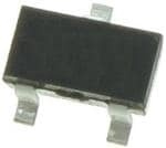
| 描述 | IC HALL EFFECT SW SC59-3板机接口霍耳效应/磁性传感器 Value Opt Hall Eff SW Ind/Consumer App |
| 产品分类 | 磁性传感器 - 霍尔效应,数字开关,线性,罗盘 (IC)磁性传感器 |
| 品牌 | Infineon Technologies |
| 产品手册 | |
| 产品图片 |
|
| rohs | 符合RoHS无铅 / 符合限制有害物质指令(RoHS)规范要求 |
| 产品系列 | 板机接口霍耳效应/磁性传感器,Infineon Technologies TLV4906K- |
| 数据手册 | http://www.infineon.com/dgdl/TLV4906x_DS_Rev1.0.pdf?folderId=db3a30431f848401011facc1c83b4674&fileId=db3a304320d39d590121544295e605cd |
| 产品型号 | TLV4906K |
| 产品种类 | 板机接口霍耳效应/磁性传感器 |
| 供应商器件封装 | SC-59 |
| 其它名称 | TLV4906KCT |
| 包装 | 剪切带 (CT) |
| 商标 | Infineon Technologies |
| 安装风格 | SMD/SMT |
| 封装 | Reel |
| 封装/外壳 | TO-236-3,SC-59,SOT-23-3 |
| 封装/箱体 | SOT-23-3 |
| 工作温度 | -40°C ~ 85°C |
| 工作点最小值/最大值 | 6.2 mT, 13.9 mT |
| 工作电源电压 | 2.7 V to 18 V |
| 工厂包装数量 | 3000 |
| 感应范围 | 10mT 跳闸, 8.5mT 释放 |
| 最大工作温度 | + 85 C |
| 最大输出电流 | 20 mA |
| 最小/最大释放点(Brp) | 4.7 mT, 12.3 mT |
| 最小工作温度 | - 40 C |
| 标准包装 | 1 |
| 特性 | - |
| 电压-电源 | 2.7 V ~ 18 V |
| 电流-电源 | 4mA |
| 电流-输出(最大值) | 20mA |
| 电源电压-最大 | 18 V |
| 电源电压-最小 | 2.7 V |
| 电源电流 | 4 mA |
| 类型 | 单极开关 |
| 系列 | TLV4906 |
| 输出电压 | 18 V |
| 输出类型 | 数字式,开漏极 |
| 零件号别名 | SP000604310 TLV4906KFTSA1 |


- 商务部:美国ITC正式对集成电路等产品启动337调查
- 曝三星4nm工艺存在良率问题 高通将骁龙8 Gen1或转产台积电
- 太阳诱电将投资9.5亿元在常州建新厂生产MLCC 预计2023年完工
- 英特尔发布欧洲新工厂建设计划 深化IDM 2.0 战略
- 台积电先进制程称霸业界 有大客户加持明年业绩稳了
- 达到5530亿美元!SIA预计今年全球半导体销售额将创下新高
- 英特尔拟将自动驾驶子公司Mobileye上市 估值或超500亿美元
- 三星加码芯片和SET,合并消费电子和移动部门,撤换高东真等 CEO
- 三星电子宣布重大人事变动 还合并消费电子和移动部门
- 海关总署:前11个月进口集成电路产品价值2.52万亿元 增长14.8%


PDF Datasheet 数据手册内容提取
TLV4906K Value Optimized Hall Effect Switch for Industrial and Consumer Applications Datasheet Rev. 1.1, 2010-08-02 Sense and Control
Edition 2010-08-02 Published by Infineon Technologies AG 81726 Munich, Germany © 2010 Infineon Technologies AG All Rights Reserved. Legal Disclaimer The information given in this document shall in no event be regarded as a guarantee of conditions or characteristics. With respect to any examples or hints given herein, any typical values stated herein and/or any information regarding the application of the device, Infineon Technologies hereby disclaims any and all warranties and liabilities of any kind, including without limitation, warranties of non-infringement of intellectual property rights of any third party. Information For further information on technology, delivery terms and conditions and prices, please contact the nearest Infineon Technologies Office (www.infineon.com). Warnings Due to technical requirements, components may contain dangerous substances. For information on the types in question, please contact the nearest Infineon Technologies Office. Infineon Technologies components may be used in life-support devices or systems only with the express written approval of Infineon Technologies, if a failure of such components can reasonably be expected to cause the failure of that life-support device or system or to affect the safety or effectiveness of that device or system. Life support devices or systems are intended to be implanted in the human body or to support and/or maintain and sustain and/or protect human life. If they fail, it is reasonable to assume that the health of the user or other persons may be endangered.
TLV4906K Value Optimized Hall Effect Switch for Industrial and Consumer Applications Revision History: 2010-08-02, Rev. 1.1 Previous Revisions: none Page Subjects (major changes since last revision) all package changed to halogen free We Listen to Your Comments Any information within this document that you feel is wrong, unclear or missing at all? Your feedback will help us to continuously improve the quality of this document. Please send your proposal (including a reference to this document) to: sensors@infineon.com Datasheet 3 Rev. 1.1, 2010-08-02
TLV4906K Table of Contents Table of Contents Table of Contents . . . . . . . . . . . . . . . . . . . . . . . . . . . . . . . . . . . . . . . . . . . . . . . . . . . . . . . . . . . . . . . . 4 List of Figures . . . . . . . . . . . . . . . . . . . . . . . . . . . . . . . . . . . . . . . . . . . . . . . . . . . . . . . . . . . . . . . . . . . 5 List of Tables . . . . . . . . . . . . . . . . . . . . . . . . . . . . . . . . . . . . . . . . . . . . . . . . . . . . . . . . . . . . . . . . . . . . 6 1 Product Description . . . . . . . . . . . . . . . . . . . . . . . . . . . . . . . . . . . . . . . . . . . . . . . . . . . . . . . . . . . . . . 7 1.1 Overview . . . . . . . . . . . . . . . . . . . . . . . . . . . . . . . . . . . . . . . . . . . . . . . . . . . . . . . . . . . . . . . . . . . . . . . . 7 1.2 Features . . . . . . . . . . . . . . . . . . . . . . . . . . . . . . . . . . . . . . . . . . . . . . . . . . . . . . . . . . . . . . . . . . . . . . . . 7 1.3 Target Applications . . . . . . . . . . . . . . . . . . . . . . . . . . . . . . . . . . . . . . . . . . . . . . . . . . . . . . . . . . . . . . . . 7 2 Functional Description . . . . . . . . . . . . . . . . . . . . . . . . . . . . . . . . . . . . . . . . . . . . . . . . . . . . . . . . . . . . 8 2.1 General . . . . . . . . . . . . . . . . . . . . . . . . . . . . . . . . . . . . . . . . . . . . . . . . . . . . . . . . . . . . . . . . . . . . . . . . . 8 2.2 Pin Configuration . . . . . . . . . . . . . . . . . . . . . . . . . . . . . . . . . . . . . . . . . . . . . . . . . . . . . . . . . . . . . . . . . 8 2.3 Pin Description . . . . . . . . . . . . . . . . . . . . . . . . . . . . . . . . . . . . . . . . . . . . . . . . . . . . . . . . . . . . . . . . . . . 9 2.4 Block Diagram . . . . . . . . . . . . . . . . . . . . . . . . . . . . . . . . . . . . . . . . . . . . . . . . . . . . . . . . . . . . . . . . . . . 9 2.5 Operating Modes and States . . . . . . . . . . . . . . . . . . . . . . . . . . . . . . . . . . . . . . . . . . . . . . . . . . . . . . . 10 2.6 Functional Block Description . . . . . . . . . . . . . . . . . . . . . . . . . . . . . . . . . . . . . . . . . . . . . . . . . . . . . . . 10 3 Specification . . . . . . . . . . . . . . . . . . . . . . . . . . . . . . . . . . . . . . . . . . . . . . . . . . . . . . . . . . . . . . . . . . . 11 3.1 Application circuit . . . . . . . . . . . . . . . . . . . . . . . . . . . . . . . . . . . . . . . . . . . . . . . . . . . . . . . . . . . . . . . . 11 3.2 Absolute Maximum Ratings . . . . . . . . . . . . . . . . . . . . . . . . . . . . . . . . . . . . . . . . . . . . . . . . . . . . . . . . 11 3.3 Operating Range . . . . . . . . . . . . . . . . . . . . . . . . . . . . . . . . . . . . . . . . . . . . . . . . . . . . . . . . . . . . . . . . 12 3.4 Electrical Characteristics . . . . . . . . . . . . . . . . . . . . . . . . . . . . . . . . . . . . . . . . . . . . . . . . . . . . . . . . . . 12 4 Package Information . . . . . . . . . . . . . . . . . . . . . . . . . . . . . . . . . . . . . . . . . . . . . . . . . . . . . . . . . . . . 14 4.1 TLV4906K Package Outline . . . . . . . . . . . . . . . . . . . . . . . . . . . . . . . . . . . . . . . . . . . . . . . . . . . . . . . . 14 Datasheet 4 Rev. 1.1, 2010-08-02
TLV4906K List of Figures List of Figures Figure 1 Pin Configuration and sensitive area (Top view, figure not to scale) . . . . . . . . . . . . . . . . . . . . . . . . 8 Figure 2 TLV4906K Block Diagram . . . . . . . . . . . . . . . . . . . . . . . . . . . . . . . . . . . . . . . . . . . . . . . . . . . . . . . . 9 Figure 3 Definition of the Magnetic Field direction . . . . . . . . . . . . . . . . . . . . . . . . . . . . . . . . . . . . . . . . . . . . 10 Figure 4 Output Signal . . . . . . . . . . . . . . . . . . . . . . . . . . . . . . . . . . . . . . . . . . . . . . . . . . . . . . . . . . . . . . . . . 10 Figure 5 Application circuit . . . . . . . . . . . . . . . . . . . . . . . . . . . . . . . . . . . . . . . . . . . . . . . . . . . . . . . . . . . . . . 11 Figure 6 Timing Diagram . . . . . . . . . . . . . . . . . . . . . . . . . . . . . . . . . . . . . . . . . . . . . . . . . . . . . . . . . . . . . . . 13 Figure 7 Marking of the TLV4906K and distance of the chip to the upper side . . . . . . . . . . . . . . . . . . . . . . 14 Figure 8 PG-SC59-3-5 Package Outline. . . . . . . . . . . . . . . . . . . . . . . . . . . . . . . . . . . . . . . . . . . . . . . . . . . . 14 Figure 9 Footprint PG-SC59-3-5 (SOT23 compatible) . . . . . . . . . . . . . . . . . . . . . . . . . . . . . . . . . . . . . . . . . 15 Datasheet 5 Rev. 1.1, 2010-08-02
TLV4906K List of Tables List of Tables Table 1 PIN Definitions for the PG-SC59-3-5 package . . . . . . . . . . . . . . . . . . . . . . . . . . . . . . . . . . . . . . . . 9 Table 2 Absolute Maximum Ratings . . . . . . . . . . . . . . . . . . . . . . . . . . . . . . . . . . . . . . . . . . . . . . . . . . . . . . 11 Table 3 Operating Range . . . . . . . . . . . . . . . . . . . . . . . . . . . . . . . . . . . . . . . . . . . . . . . . . . . . . . . . . . . . . . 12 Table 4 Electrical Characteristics . . . . . . . . . . . . . . . . . . . . . . . . . . . . . . . . . . . . . . . . . . . . . . . . . . . . . . . . 12 Table 5 Magnetic Characteristics . . . . . . . . . . . . . . . . . . . . . . . . . . . . . . . . . . . . . . . . . . . . . . . . . . . . . . . . 13 Datasheet 6 Rev. 1.1, 2010-08-02
Hall Effect Switch TLV4906K 1 Product Description 1.1 Overview The TLV4906K is a high precision Hall Effect Switch with highly accurate switching thresholds for ambient operating temperatures up to 85°C. The TLV4906K is available in a SMD package PG-SC59-3-5 which is lead-free and halogen-free to meet current und future requirements. 1.2 Features • 2.7 V to 18 V supply voltage operation. • Operation from unregulated power supply. • High sensitivity and high stability of the magnetic switching points. • High resistance to mechanical stress by active error compensation. • Reverse battery protection (-18 V). • Superior temperature stability. • Low jitter (typically 1 µs). • High ESD performance (± 4 kV HBM). • Digital output signal (open-drain). • Lead-free and halogen-free green SMD package • Not suitable for automotive applications 1.3 Target Applications The TLV4906K is ideally suited for all industrial and consumer applications that require a high precision switching thresholds for position sensing. It can be used for example for: security systems, alignment control, push buttons, keyboards, key switches, machine tools, etc. Product Name Product Type Ordering Code Package TLV4906K Hall Effect Switch SP000604310 PG-SC59-3-5 Datasheet 7 Rev. 1.1, 2010-08-02
TLV4906K Functional Description 2 Functional Description 2.1 General Precise magnetic switching thresholds and high temperature stability are achieved by active compensation circuits and chopper techniques on chip. Offset voltages generated by temperature-induced stress or overmolding are canceled so that high accuracy is achieved. The IC has an open collector output stage with 20 mA current sink capability. A wide operating voltage range from 2.7 V to 18 V with reverse polarity protection down to -18 V makes the TLV4906K suitable for a wide range of applications. A magnetic south pole with a field strength above B turns op the output transistor on (output voltage low) and for a magnetic field below B the output transistor is switched off rp (output voltage high). 2.2 Pin Configuration Center of Sensitive Area 3 0.8 ± 0.15 1 2 1.5 ± 0.15 SC59 Figure 1 Pin Configuration and sensitive area (Top view, figure not to scale) Datasheet 8 Rev. 1.1, 2010-08-02
TLV4906K Functional Description 2.3 Pin Description Table 1 PIN Definitions for the PG-SC59-3-5 package PIN No. Name Function 1 V Supply Voltage s 2 Q Output 3 GND Ground 2.4 Block Diagram V S Voltage Regulator reverse polarity protected Bias and Oscillator Compensation and Circuits Sequencer Q Ref GND Amplifier Low Comparator Chopped Pass with Hall Probe Filter Hysteresis Figure 2 TLV4906K Block Diagram Datasheet 9 Rev. 1.1, 2010-08-02
TLV4906K Functional Description 2.5 Operating Modes and States Field Direction and Definition Positive magnetic fields correspond to the south pole of the magnet targeting the branded side of the package. N S Branded Side Figure 3 Definition of the Magnetic Field direction V Q B 0 B B rp op Figure 4 Output Signal 2.6 Functional Block Description The chopped Hall Effect Switch comprises a Hall probe, a bias generator, compensation circuits, an oscillator and an output transistor. The bias generator provides currents to the Hall probe and the active circuits. Compensation circuits stabilize response of the IC over temperature and reduce the impact of process variations. The Active Error Compensation rejects offsets in the signal path and reduces the impact of mechanical stress in the package caused by molding, soldering and thermal effects. The chopper technique together with the threshold generator and the comparator ensure high accurate magnetic switching points. Datasheet 10 Rev. 1.1, 2010-08-02
TLV4906K Specification 3 Specification 3.1 Application circuit Q Q X F 6 7n 90 GND 4. GND kΩ 4 2 V F 1. n L 7 T VS 4. 200Ω VS Figure 5 Application circuit It is recommended to use a resistor of 200 Ω in the supply line for current limitation in the case of an overvoltage pulse. Two capacitors of 4.7 nF enhance the EMC performance. The pull-up of 1.2 kΩ limits the current through the output transistor. 3.2 Absolute Maximum Ratings Stress above the maximum values listed in this section may cause permanent damage to the device. Exposure to absolute maximum rating conditions for extended periods may affect the reliability of the device. Exceeding only one of these values may cause irreversible damage to the device. Table 2 Absolute Maximum Ratings Parameter Symbol Values Unit Note / Test Condition Min. Typ. Max. Maximum Ambient Temperature T - 40 – 125 °C A Maximum Junction Temperature T - 40 – 150 °C J Supply Voltage V - 18 – 18 V S Supply current through protection I -50 – 50 mA S device Output Voltage V - 0.7 – 18 V OUT Storage Temperature T - 40 – 150 °C S Magnetic flux density B – – unlimited mT ESD Robustness HBM: V 1) – – 4 kV ESD,HBM 1.5 kΩ, 100 pF 1) According to EIA/JESD22-A114-E Datasheet 11 Rev. 1.1, 2010-08-02
TLV4906K Specification 3.3 Operating Range The following operating conditions must not be exceeded in order to ensure correct operation of the TLV4906K. All parameters specified in the following sections refer to these operating conditions unless otherwise mentioned. Table 3 Operating Range Parameter Symbol Values Unit Note / Test Condition Min. Typ. Max. Supply Voltage V 2.7 – 18 V S Output Voltage V -0.7 – 18 V Q Output Current I 0 – 20 mA Q Maximum Ambient Temperature T -40 – 85 °C A 3.4 Electrical Characteristics Product characteristics include the spread of values guaranteed within the specified voltage and ambient temperature range. typical characteristics are the median of the production (at V =12V and T =25°C). s A Table 4 Electrical Characteristics Parameter Symbol Values Unit Note / Test Condition Min. Typ. Max. Supply Current I 2 4 6 mA V =2.7 V...18 V S S Reverse Current I 0 0.2 1 mA V =-18 V SR S Output Saturation Voltage V – 0.3 0.6 V I =20 mA QSAT Q Output leakage current I – 0.05 10 µA V =18 V QLEAK Q Output fall time1) t – 0.02 1 µs R =1.2k Ω, C =50 pF f L L Output rise time1) t – 0.4 1 µs r Chopper frequency f – 320 – kHz OSC Switching frequency f 0 – 152) kHz SW Delay time3) t – 13 – µs d Output jitter4) t – 1 – µs Typical value for a 1 kHz QJ RMS square wave signal Power-on Time5) t – 13 – µs V > 2.7 V PON S Thermal Resistance junction to R – 100 – K/W TLV4906K thja ambient6) 1) See Figure 6 2) To operate the sensor at maximum switching frequency, the value of the magnetic signal amplitude must be 1.4 times higher than the static fields. This is due to the -3 dB corner frequency of the low pass filter in the signal path. 3) Systematic delay between magnetic threshold reached and output. 4) Jitter is the unpredictable deviation of the output switching delay. 5) Time from applying V . > 2.7 V to the sensor until the output state is valid. S 6) Relationship between junction and ambient temperature: T =T + R . (V . I + V . I ). J amb thja S S QS Q Datasheet 12 Rev. 1.1, 2010-08-02
TLV4906K Specification Applied Magnetic B Field OP B RP t t d d t t f r V Q 90% 10% Figure 6 Timing Diagram Table 5 Magnetic Characteristics 1) Parameter Symbol Values Unit Note / Test Condition Min. Typ. Max. Operate point B 6.2 10.0 13.9 mT OP Release point B 4.7 8.5 12.3 mT RP Hysteresis B 0.7 1.5 3.0 mT 2) HYS Temperature compensation of TC – -350 – ppm/°C magnetic thresholds Repeatability of magnetic B – 20 – µT typical value for REP RMS thresholds3) ΔΒ/Δt > 12mT/ms 1) Over all operating conditions. 2) At 25°C. 3) B is equivalent to the noise constant. REP Datasheet 13 Rev. 1.1, 2010-08-02
TLV4906K Package Information 4 Package Information 4.1 TLV4906K Package Outline Branded Side Year (y) = 0...9 VB1 m Month (m) = 1...9, d o-October y n-November d-December d: Distance chip to upper side of IC: d = 0.56±0.1mm AEA03244 Figure 7 Marking of the TLV4906K and distance of the chip to the upper side 1.1±0.1 3±0.1 0.15 MAX. 0.1 3x0.4+-00..105 0.2+0.1 0.1M 3 5 +0.2-0.1 5±0.1 +0.15-0.3 8 4 6 2. 0. 1. 1 2 0.95 0.15+0.1 -0.05 0.95 M 1 0. (0.55) 0˚...8˚ MAX. GPS09473 Figure 8 PG-SC59-3-5 Package Outline Datasheet 14 Rev. 1.1, 2010-08-02
TLV4906K Package Information 0.8 0.8 n mi 0.9 1.4 3 1. 1.6 9 0. n mi 1.2 4 1. 0.8 1.2 0.8 Reflow Soldering Wave Soldering Figure 9 Footprint PG-SC59-3-5 (SOT23 compatible) Datasheet 15 Rev. 1.1, 2010-08-02
www.infineon.com Published by Infineon Technologies AG
Mouser Electronics Authorized Distributor Click to View Pricing, Inventory, Delivery & Lifecycle Information: I nfineon: TLV4906K TLV4906L