ICGOO在线商城 > 集成电路(IC) > 线性 - 放大器 - 仪表,运算放大器,缓冲器放大器 > TLV4120IDGN
 Datasheet下载
- 型号: TLV4120IDGN
- 制造商: Texas Instruments
- 库位|库存: xxxx|xxxx
- 要求:
| 数量阶梯 | 香港交货 | 国内含税 |
| +xxxx | $xxxx | ¥xxxx |
查看当月历史价格
查看今年历史价格
TLV4120IDGN产品简介:
ICGOO电子元器件商城为您提供TLV4120IDGN由Texas Instruments设计生产,在icgoo商城现货销售,并且可以通过原厂、代理商等渠道进行代购。 TLV4120IDGN价格参考。Texas InstrumentsTLV4120IDGN封装/规格:线性 - 放大器 - 仪表,运算放大器,缓冲器放大器, 通用 放大器 1 电路 差分 8-MSOP-PowerPad。您可以下载TLV4120IDGN参考资料、Datasheet数据手册功能说明书,资料中有TLV4120IDGN 详细功能的应用电路图电压和使用方法及教程。
TLV4120IDGN 是 Texas Instruments(德州仪器)生产的一款高精度、低功耗的运算放大器,属于线性放大器类别中的仪表、运算放大器和缓冲器放大器。该器件具有低失调电压、低温漂、高开环增益和出色的共模抑制比(CMRR)等特性,适用于对精度要求较高的模拟信号处理场合。

其典型应用场景包括:

1. 传感器信号调理:如温度、压力、应变片等传感器的微弱信号放大,适合在工业自动化与测量系统中使用;
2. 精密模拟前端:用于数据采集系统中,作为前置放大器或缓冲器,提升信号质量;
3. 电池供电设备:由于其低功耗特性,适用于便携式仪器、手持测试设备和远程监测系统;
4. 医疗电子设备:如心电图机、血糖仪等需要高稳定性和低噪声的医疗检测设备;
5. 音频与通信系统:用于低噪声前置放大、滤波电路及信号隔离缓冲等环节;
6. 工业控制与过程控制:在PLC(可编程逻辑控制器)、执行器反馈电路中实现精确控制。

TLV4120IDGN采用8引脚TSSOP封装,便于集成于紧凑型电路设计中,是追求高性能与稳定性应用的理想选择。
| 参数 | 数值 |
| -3db带宽 | - |
| 产品目录 | 集成电路 (IC)半导体 |
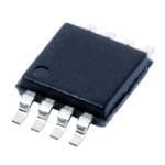
| 描述 | IC OPAMP GP 2.4MHZ 8MSOP运算放大器 - 运放 High Output Drive Differential |
| 产品分类 | Linear - Amplifiers - Instrumentation, OP Amps, Buffer Amps集成电路 - IC |
| 品牌 | Texas Instruments |
| 产品手册 | |
| 产品图片 |
|
| rohs | 符合RoHS无铅 / 符合限制有害物质指令(RoHS)规范要求 |
| 产品系列 | 放大器 IC,运算放大器 - 运放,Texas Instruments TLV4120IDGN- |
| 数据手册 | |
| 产品型号 | TLV4120IDGN |
| 产品种类 | 运算放大器 - 运放 |
| 供应商器件封装 | 8-MSOP-PowerPad |
| 共模抑制比—最小值 | 71 dB |
| 关闭 | Shutdown |
| 包装 | 管件 |
| 单位重量 | 19 mg |
| 压摆率 | 1.57 V/µs |
| 商标 | Texas Instruments |
| 增益带宽生成 | 2.4 MHz |
| 增益带宽积 | 2.4MHz |
| 安装类型 | 表面贴装 |
| 安装风格 | SMD/SMT |
| 封装 | Tube |
| 封装/外壳 | 8-TSSOP,8-MSOP(0.118",3.00mm 宽)裸焊盘 |
| 封装/箱体 | HVSSOP-8 |
| 工作温度 | -40°C ~ 85°C |
| 工作电源电压 | 2.7 V to 5.5 V |
| 工厂包装数量 | 80 |
| 技术 | CMOS |
| 放大器类型 | High Output Drive Amplifier |
| 最大工作温度 | + 85 C |
| 最小工作温度 | - 40 C |
| 标准包装 | 80 |
| 电压-电源,单/双 (±) | 2.7 V ~ 5.5 V |
| 电压-输入失调 | 100µV |
| 电流-电源 | 1.4mA |
| 电流-输入偏置 | 0.3pA |
| 电流-输出/通道 | 320mA |
| 电源电流 | 1.7 mA |
| 电路数 | 1 |
| 系列 | TLV4120 |
| 转换速度 | 1.57 V/us |
| 输入偏压电流—最大 | 60 pA |
| 输入参考电压噪声 | 10 nV |
| 输入补偿电压 | 3 mV |
| 输出电流 | 320 mA |
| 输出类型 | 差分 |
| 通道数量 | 1 Channel |


- 商务部:美国ITC正式对集成电路等产品启动337调查
- 曝三星4nm工艺存在良率问题 高通将骁龙8 Gen1或转产台积电
- 太阳诱电将投资9.5亿元在常州建新厂生产MLCC 预计2023年完工
- 英特尔发布欧洲新工厂建设计划 深化IDM 2.0 战略
- 台积电先进制程称霸业界 有大客户加持明年业绩稳了
- 达到5530亿美元!SIA预计今年全球半导体销售额将创下新高
- 英特尔拟将自动驾驶子公司Mobileye上市 估值或超500亿美元
- 三星加码芯片和SET,合并消费电子和移动部门,撤换高东真等 CEO
- 三星电子宣布重大人事变动 还合并消费电子和移动部门
- 海关总署:前11个月进口集成电路产品价值2.52万亿元 增长14.8%


PDF Datasheet 数据手册内容提取
(cid:1)(cid:2)(cid:3)(cid:4)(cid:5)(cid:6)(cid:7) (cid:8)(cid:9)(cid:10)(cid:8) (cid:11)(cid:12)(cid:1)(cid:13)(cid:12)(cid:1) (cid:14)(cid:12)(cid:15)(cid:15)(cid:16)(cid:17)(cid:1) (cid:18)(cid:9)(cid:19)(cid:19)(cid:16)(cid:15)(cid:16)(cid:17)(cid:1)(cid:9)(cid:20)(cid:2) (cid:18)(cid:15)(cid:9)(cid:3)(cid:16) (cid:11)(cid:13)(cid:16)(cid:15)(cid:20)(cid:1)(cid:9)(cid:11)(cid:17)(cid:20)(cid:2) (cid:20)(cid:21)(cid:13)(cid:2)(cid:9)(cid:19)(cid:9)(cid:16)(cid:15) (cid:22)(cid:9)(cid:1)(cid:8) (cid:23)(cid:8)(cid:12)(cid:1)(cid:18)(cid:11)(cid:22)(cid:17) SLOS310B − DECEMBER 2000 − REVISED SEPTEMBER 2006 (cid:1) High Output Current Differential DGN PACKAGE Drive...>200 mA (TOP VIEW) (cid:1) Rail-To-Rail Output (cid:1) SHDN 1 8 VO− Unity-Gain Bandwidth...2.4 MHz VDD/2 2 7 GND (cid:1) Slew Rate...1.5 V/µs IN+ 3 6 VDD (cid:1) Supply Current...1.4 mA IN− 4 5 VO+ (cid:1) Supply Voltage Range...2.7 V to 5.5 V (cid:1) Specified Temperature Range: − T = −40°C to 85°C...Industrial Grade A description The TLV4120 single supply operational differential amplifier provides a differential output current in excess of 200 mA at 5 V. This enables the amplifier to be used as high current line drivers, buffers, or coil driver applications. The TLV4120 has a shutdown feature that reduces the supply current down to 6 µA when the amplifier is not active in the application. The TLV4120 is available in the ultrasmall MSOP PowerPAD package, which offers the exceptional thermal impedance required for amplifiers delivering high current levels. AVAILABLE OPTIONS NNUUMMBBEERR OOFF PACKAGE TYPES TTAA DDEEVVIICCEE CHANNELS MSOP (DGN)† SSYYMMBBOOLL SSHHUUTTDDOOWWNN −40°C to 85°C TLV4120 1 TLV4120IDGN xxTIAHU Yes †This package is available taped and reeled. To order this packaging option, add an R suffix to the part number (e.g., TLV4120IDGNR). functional block diagram VDD 6 4 IN− − VO+ 5 A1 3 IN+ + 2 VDD/2 − VO− 8 A2 + 7 GND 1 SHDN Bias Control Please be aware that an important notice concerning availability, standard warranty, and use in critical applications of TexasInstruments semiconductor products and disclaimers thereto appears at the end of this data sheet. PowerPAD is a trademark of Texas Instruments. All other trademarks are the property of their respective owners. (cid:13)(cid:15)(cid:11)(cid:18)(cid:12)(cid:14)(cid:1)(cid:9)(cid:11)(cid:17) (cid:18)(cid:20)(cid:1)(cid:20) (cid:24)(cid:25)(cid:26)(cid:27)(cid:28)(cid:29)(cid:30)(cid:31)(cid:24)(cid:27)(cid:25) (cid:24)! "#(cid:28)(cid:28)$(cid:25)(cid:31) (cid:30)! (cid:27)(cid:26) %#&’(cid:24)"(cid:30)(cid:31)(cid:24)(cid:27)(cid:25) ((cid:30)(cid:31)$) Copyright 2000−2006, Texas Instruments Incorporated (cid:13)(cid:28)(cid:27)(#"(cid:31)! "(cid:27)(cid:25)(cid:26)(cid:27)(cid:28)(cid:29) (cid:31)(cid:27) !%$"(cid:24)(cid:26)(cid:24)"(cid:30)(cid:31)(cid:24)(cid:27)(cid:25)! %$(cid:28) (cid:31)*$ (cid:31)$(cid:28)(cid:29)! (cid:27)(cid:26) (cid:1)$+(cid:30)! (cid:9)(cid:25)!(cid:31)(cid:28)#(cid:29)$(cid:25)(cid:31)! !(cid:31)(cid:30)(cid:25)((cid:30)(cid:28)( ,(cid:30)(cid:28)(cid:28)(cid:30)(cid:25)(cid:31)-) (cid:13)(cid:28)(cid:27)(#"(cid:31)(cid:24)(cid:27)(cid:25) %(cid:28)(cid:27)"$!!(cid:24)(cid:25). ((cid:27)$! (cid:25)(cid:27)(cid:31) (cid:25)$"$!!(cid:30)(cid:28)(cid:24)’- (cid:24)(cid:25)"’#($ (cid:31)$!(cid:31)(cid:24)(cid:25). (cid:27)(cid:26) (cid:30)’’ %(cid:30)(cid:28)(cid:30)(cid:29)$(cid:31)$(cid:28)!) POST OFFICE BOX 655303 • DALLAS, TEXAS 75265 1
(cid:1)(cid:2)(cid:3)(cid:4)(cid:5)(cid:6)(cid:7) (cid:8)(cid:9)(cid:10)(cid:8) (cid:11)(cid:12)(cid:1)(cid:13)(cid:12)(cid:1) (cid:14)(cid:12)(cid:15)(cid:15)(cid:16)(cid:17)(cid:1) (cid:18)(cid:9)(cid:19)(cid:19)(cid:16)(cid:15)(cid:16)(cid:17)(cid:1)(cid:9)(cid:20)(cid:2) (cid:18)(cid:15)(cid:9)(cid:3)(cid:16) (cid:11)(cid:13)(cid:16)(cid:15)(cid:20)(cid:1)(cid:9)(cid:11)(cid:17)(cid:20)(cid:2) (cid:20)(cid:21)(cid:13)(cid:2)(cid:9)(cid:19)(cid:9)(cid:16)(cid:15) (cid:22)(cid:9)(cid:1)(cid:8) (cid:23)(cid:8)(cid:12)(cid:1)(cid:18)(cid:11)(cid:22)(cid:17) SLOS310B − DECEMBER 2000 − REVISED SEPTEMBER 2006 absolute maximum ratings over operating free-air temperature range (unless otherwise noted)† Supply voltage, V (see Note 1) . . . . . . . . . . . . . . . . . . . . . . . . . . . . . . . . . . . . . . . . . . . . . . . . . . . . . . . . . . . . . 6 V DD Differential input voltage, V . . . . . . . . . . . . . . . . . . . . . . . . . . . . . . . . . . . . . . . . . . . . . . . . . . . . . . . . . . . . . . ±V ID DD Input voltage range, V . . . . . . . . . . . . . . . . . . . . . . . . . . . . . . . . . . . . . . . . . . . . . . . . . . . . . . . . . . . . . . . . . . . . ±V I DD Output current,I (see Note 2) . . . . . . . . . . . . . . . . . . . . . . . . . . . . . . . . . . . . . . . . . . . . . . . . . . . . . . . . . . . . 800 mA O Continuous /RMS output current, I (each output of amplifier): T ≤ 105°C . . . . . . . . . . . . . . . . . . . . 350 mA O J T ≤ 150°C . . . . . . . . . . . . . . . . . . . . 110 mA J Peak output current, I (each output of amplifier: T ≤ 105°C . . . . . . . . . . . . . . . . . . . . . . . . . . . . . . . . 500 mA O J T ≤ 150°C . . . . . . . . . . . . . . . . . . . . . . . . . . . . . . . . 155 mA J Continuous total power dissipation . . . . . . . . . . . . . . . . . . . . . . . . . . . . . . . . . . . . . See Dissipation Rating Table Operating free-air temperature range, T : I suffix . . . . . . . . . . . . . . . . . . . . . . . . . . . . . . . . . . . . . −40°C to 85°C A Maximum junction temperature, T . . . . . . . . . . . . . . . . . . . . . . . . . . . . . . . . . . . . . . . . . . . . . . . . . . . . . . . . . 150°C J Storage temperature range, T . . . . . . . . . . . . . . . . . . . . . . . . . . . . . . . . . . . . . . . . . . . . . . . . . . . −65°C to 150°C stg Lead temperature 1,6 mm (1/16 inch) from case for 10 seconds . . . . . . . . . . . . . . . . . . . . . . . . . . . . . . . 260°C †Stresses beyond those listed under “absolute maximum ratings” may cause permanent damage to the device. These are stress ratings only, and functional operation of the device at these or any other conditions beyond those indicated under “recommended operating conditions” is not implied. Exposure to absolute-maximum-rated conditions for extended periods may affect device reliability. NOTES: 1. All voltage values, except differential voltages, are with respect to GND. 2. To prevent permanent damage the die temperature must not exceed the maximum junction temperature. DISSIPATION RATING TABLE θJC θJA TA ≤ 25°C TA = 85°C PACKAGE (°C/W) (°C/W) POWER RATING POWER RATING DGN (8)‡ 4.7 52.7 2.37 W 1.23 W ‡See The Texas Instruments document, PowerPAD Thermally Enhanced Package Application Report (literature number SLMA002), for more information on the PowerPAD package. The thermal data was measured on a PCB layout based on the information in the section entitled Texas Instruments Recommended Board for PowerPAD on page 33 of the before mentioned document. recommended operating conditions MIN MAX UNIT Supply voltage, VDD 2.7 5.5 V Common-mode input voltage range, VICR 0.5 VDD−0.5 V Operating free-air temperature, TA I-suffix −40 85 °C V(on) <VDD/3 SShhuuttddoowwnn ttuurrnn--oonn//ooffff vvoollttaaggee lleevveell§§ V(off) >VDD×0.75 VV §Relative to GND 2 POST OFFICE BOX 655303 • DALLAS, TEXAS 75265
(cid:1)(cid:2)(cid:3)(cid:4)(cid:5)(cid:6)(cid:7) (cid:8)(cid:9)(cid:10)(cid:8) (cid:11)(cid:12)(cid:1)(cid:13)(cid:12)(cid:1) (cid:14)(cid:12)(cid:15)(cid:15)(cid:16)(cid:17)(cid:1) (cid:18)(cid:9)(cid:19)(cid:19)(cid:16)(cid:15)(cid:16)(cid:17)(cid:1)(cid:9)(cid:20)(cid:2) (cid:18)(cid:15)(cid:9)(cid:3)(cid:16) (cid:11)(cid:13)(cid:16)(cid:15)(cid:20)(cid:1)(cid:9)(cid:11)(cid:17)(cid:20)(cid:2) (cid:20)(cid:21)(cid:13)(cid:2)(cid:9)(cid:19)(cid:9)(cid:16)(cid:15) (cid:22)(cid:9)(cid:1)(cid:8) (cid:23)(cid:8)(cid:12)(cid:1)(cid:18)(cid:11)(cid:22)(cid:17) SLOS310B − DECEMBER 2000 − REVISED SEPTEMBER 2006 electrical characteristics at recommend operating conditions, V = 2.7 V and 5 V (unless DD otherwise noted) dc performance PARAMETER TEST CONDITIONS TA† MIN TYP MAX UNITS VVIIOO IInnppuutt ooffffsseett vvoollttaaggee VVIICC == VVDDDD//22,, VVROOS === 5VV0DD ΩDD//22 ,, Fu2ll 5r°aCnge 100 34000000 µVV VVDDDD == 22..77 VV,, VVIICC == 00..55 ttoo 22..22 VV,, 25°C 69 95 RS = 50 Ω Full range 66 CCMMRRRR CCoommmmoonn--mmooddee rreejjeeccttiioonn rraattiioo ddBB VVDDDD == 55 VV,, VVIICC == 00..55 ttoo 44..55 VV,, 25°C 71 95 RS = 50 Ω Full range 68 VDDDD = 2.7 V, 25°C 80 85 VVOO((PPPP))==11 VV,, RRLL==110000 ΩΩ LLaarrggee--ssiiggnnaall ddiiffffeerreennttiiaall vvoollttaaggee VIC = VDD/2 Full range 70 AAVVDD amplification VDDDD = 5 V, 25°C 90 95 ddBB VVOO((PPPP))==33 VV,, RRLL==110000 ΩΩ VIC = VDD/2 Full range 80 †Full range is −40°C to 85°C for I suffix. input characteristics PARAMETER TEST CONDITIONS TA† MIN TYP MAX UNITS 25°C 0.3 60 IIIIIIOOO IIInnnpppuuuttt oooffffffssseeettt cccuuurrrrrreeennnttt VVVIIICCC === VVVDDDDDD///222 FFuullll rraannggee 330000 IIIIIIBBB IIInnnpppuuuttt bbbiiiaaasss cccuuurrrrrreeennnttt VVRROOSSS ==== 55VV00DD ΩΩDD//22,, 25°C 0.3 60 ppAA FFuullll rraannggee 330000 ri(d) Differential input resistance 25°C 1000 GΩ CIC Common-mode input capacitance f = 100 Hz 25°C 5 pF VDD/2 biasing resistors 25°C 500 kΩ Amplifier A2’s gain resistors 25°C 20 kΩ †Full range is −40°C to 85°C for I suffix. POST OFFICE BOX 655303 • DALLAS, TEXAS 75265 3
(cid:1)(cid:2)(cid:3)(cid:4)(cid:5)(cid:6)(cid:7) (cid:8)(cid:9)(cid:10)(cid:8) (cid:11)(cid:12)(cid:1)(cid:13)(cid:12)(cid:1) (cid:14)(cid:12)(cid:15)(cid:15)(cid:16)(cid:17)(cid:1) (cid:18)(cid:9)(cid:19)(cid:19)(cid:16)(cid:15)(cid:16)(cid:17)(cid:1)(cid:9)(cid:20)(cid:2) (cid:18)(cid:15)(cid:9)(cid:3)(cid:16) (cid:11)(cid:13)(cid:16)(cid:15)(cid:20)(cid:1)(cid:9)(cid:11)(cid:17)(cid:20)(cid:2) (cid:20)(cid:21)(cid:13)(cid:2)(cid:9)(cid:19)(cid:9)(cid:16)(cid:15) (cid:22)(cid:9)(cid:1)(cid:8) (cid:23)(cid:8)(cid:12)(cid:1)(cid:18)(cid:11)(cid:22)(cid:17) SLOS310B − DECEMBER 2000 − REVISED SEPTEMBER 2006 electrical characteristics at specified free-air temperature, V = 2.7 V and 5 V (unless DD otherwise noted) (continued) output characteristics PARAMETER TEST CONDITIONS TA† MIN TYP MAX UNITS 25°C 2.6 2.67 IIOOHH == −−1100 mmAA Full range 2.58 VVDDDD == 22..77 VV,, VVIICC == VVDDDD//22 25°C 2.35 2.4 IIOOHH ==−−110000 mmAA Full range 2.3 25°C 4.9 4.96 VVOOHH HHiigghh--lleevveell oouuttppuutt vvoollttaaggee IIOOHH == −−1100 mmAA VV Full range 4.88 25°C 4.7 4.8 VVDDDD == 55 VV,, VVIICC == VVDDDD//22 IIOOHH == −−110000 mmAA Full range 4.65 25°C 4.45 4.55 IIOOHH == −−220000 mmAA Full range 4.38 25°C 0.03 0.1 IIOOLL == 1100 mmAA Full range 0.12 VVDDDD == 22..77 VV ,, VVIICC == VVDDDD//22 25°C 0.3 0.4 IIOOLL == 110000 mmAA Full range 0.5 25°C 0.03 0.1 VVOOLL LLooww−−lleevveell oouuttppuutt vvoollttaaggee IIOOLL == 1100 mmAA VV Full range 0.12 25°C 0.2 0.3 VVDDDD == 55 VV,, VVIICC == VVDDDD//22 IIOOLL == 110000 mmAA Full range 0.35 25°C 0.5 0.55 IIOOLL == 220000 mmAA Full range 0.62 VDD = 2.7 V 320 IIOO OOuuttppuutt ccuurrrreenntt MMeeaassuurreedd aatt 00..55 VV ffrroomm rraaiill 2255°°CC mmAA VDD = 5 V 200 †Full range is−40°C to 85°C for I suffix. power supply PARAMETER TEST CONDITIONS TA MIN TYP MAX UNITS 25°C 1.4 1.7 IIDDDD SSuuppppllyy ccuurrrreenntt VVOO == VVDDDD//22,, SSHHDDNN == <<VVdddd//33 VV mmAA Full range 2.3 VVDDDD ==22..77 ttoo 33..33 VV,, 25°C 80 94 VIC = VDD/2 V, No load Full range 75 PPSSRRRR PPoowweerr ssuuppppllyy rreejjeeccttiioonn rraattiioo ((∆∆VVDDDD // ∆∆VVIIOO)) ddBB VVDDDD ==22..77 ttoo 55 VV,, 25°C 70 84 VIC = VDD/2 V, No load Full range 65 †Full range is −40°C to 85°C for I suffix. 4 POST OFFICE BOX 655303 • DALLAS, TEXAS 75265
(cid:1)(cid:2)(cid:3)(cid:4)(cid:5)(cid:6)(cid:7) (cid:8)(cid:9)(cid:10)(cid:8) (cid:11)(cid:12)(cid:1)(cid:13)(cid:12)(cid:1) (cid:14)(cid:12)(cid:15)(cid:15)(cid:16)(cid:17)(cid:1) (cid:18)(cid:9)(cid:19)(cid:19)(cid:16)(cid:15)(cid:16)(cid:17)(cid:1)(cid:9)(cid:20)(cid:2) (cid:18)(cid:15)(cid:9)(cid:3)(cid:16) (cid:11)(cid:13)(cid:16)(cid:15)(cid:20)(cid:1)(cid:9)(cid:11)(cid:17)(cid:20)(cid:2) (cid:20)(cid:21)(cid:13)(cid:2)(cid:9)(cid:19)(cid:9)(cid:16)(cid:15) (cid:22)(cid:9)(cid:1)(cid:8) (cid:23)(cid:8)(cid:12)(cid:1)(cid:18)(cid:11)(cid:22)(cid:17) SLOS310B − DECEMBER 2000 − REVISED SEPTEMBER 2006 electrical characteristics at specified free-air temperature, V = 2.7 V and 5 V (unless DD otherwise noted) (continued) dynamic performance PARAMETER TEST CONDITIONS TA† MIN TYP MAX UNITS GBWP Gain bandwidth product RL=100 Ω CL=10 pF 25°C 2.4 MHz 25°C 0.75 1.48 VVooo(((pppp))) == VVDDDD//22,, VVDDDD == 22..77 VV Full range 0.5 SSRR SSlleeww rraattee aatt uunniittyy ggaaiinn RRLL == 110000 ΩΩ,, 25°C 0.9 1.57 VV//µss CCLL == 5500 ppFF VVDDDD == 55 VV Full range 0.65 φM Phase margin 60 RRLL == 110000 ΩΩ,, CCLL == 1100 ppFF 2255°°CC Gain margin 20 dB Vn Input noise voltage f = 10 kHz 25°C 10 nV/√Hz †Full range is −40°C to 85°C for I suffix. shutdown characteristics PARAMETER TEST CONDITIONS TA† MIN TYP MAX UNITS 25°C 6 12 IIDDDD((SSHHDDNN)) SSuuppppllyy ccuurrrreenntt iinn sshhuuttddoowwnn mmooddee SSHHDDNN >> VVdddd ×× 00..7755 µAA Full range 50 †Full range is −40°C to 85°C for I suffix. TYPICAL CHARACTERISTICS Table of Graphs FIGURE VOH High-level output voltage vs High-level output current 1, 3 VOL Low-level output voltage vs Low-level output current 2, 4 ZO Output impedance vs Frequency 5 PO Output power vs Load resistance 6 IDD Supply current vs Supply voltage 7 PSRR Power supply rejection ratio vs Frequency 8 Avd Differential voltage amplification and phase vs Frequency 9 Phase margin vs Capacitive load 10 vs Free-air temperature 11 SSlleeww rraattee vs Supply voltage 12 Total harmonic distortion + noise vs Frequency 13 Inverting large-signal pulse response vs Time 14 Inverting small-signal pulse response vs Time 15 IDD(SHDN) Shutdown supply current vs Free-air temperature 16 IDD(SHDN) Shutdown supply current vs Supply voltage 17 Shutdown mode pulse response vs Time 18 POST OFFICE BOX 655303 • DALLAS, TEXAS 75265 5
(cid:1)(cid:2)(cid:3)(cid:4)(cid:5)(cid:6)(cid:7) (cid:8)(cid:9)(cid:10)(cid:8) (cid:11)(cid:12)(cid:1)(cid:13)(cid:12)(cid:1) (cid:14)(cid:12)(cid:15)(cid:15)(cid:16)(cid:17)(cid:1) (cid:18)(cid:9)(cid:19)(cid:19)(cid:16)(cid:15)(cid:16)(cid:17)(cid:1)(cid:9)(cid:20)(cid:2) (cid:18)(cid:15)(cid:9)(cid:3)(cid:16) (cid:11)(cid:13)(cid:16)(cid:15)(cid:20)(cid:1)(cid:9)(cid:11)(cid:17)(cid:20)(cid:2) (cid:20)(cid:21)(cid:13)(cid:2)(cid:9)(cid:19)(cid:9)(cid:16)(cid:15) (cid:22)(cid:9)(cid:1)(cid:8) (cid:23)(cid:8)(cid:12)(cid:1)(cid:18)(cid:11)(cid:22)(cid:17) SLOS310B − DECEMBER 2000 − REVISED SEPTEMBER 2006 TYPICAL CHARACTERISTICS HIGH-LEVEL OUTPUT VOLTAGE LOW-LEVEL OUTPUT VOLTAGE HIGH-LEVEL OUTPUT VOLTAGE vs vs vs HIGH-LEVEL OUTPUT CURRENT LOW-LEVEL OUTPUT CURRENT HIGH-LEVEL OUTPUT CURRENT 2.7 2.7 5.00 V VO = Positive & Negative VO = Positive & Negative V − High-Level Output Voltage − 0011122.......6925814 TA = 2V5°DCD = 2.7 V Low-Level Output Voltage − V 0011122.......6925814 VDD = 2.7T TVTAAA = T= = A− 2 04 5=°0° C°8CC5°C − High-Level Output Voltage − 334444......570257050505 TTTAAA T= = A= − 2 =045 °08°C°C5C°C VOH 0.3 TTAA = = − 04°0C°C TA = 85°C V− OL 0.3 VOH3.25 VVODD = =P o5s Vitive & Negative 0.0 0.0 3.00 0 50 100 150 200 250 300 350 400 450 0 50 100 150 200 250 300 350 0 50 100150200250300350400450500 IOH − High-Level Output Current − mA IOL − Low-Level Output Current − mA IOH − High-Level Output Current − mA Figure 1 Figure 2 Figure 3 LOW-LEVEL OUTPUT VOLTAGE OUTPUT IMPEDANCE OUTPUT POWER vs vs vs LOW-LEVEL OUTPUT CURRENT FREQUENCY LOAD RESISTANCE 1.0 ge − V 00..89 VVODD = =P o5s Vitive & Negative Ω 1010000 VTAD D= 2=5 2°. 7C V & 5 V W 870000 Tf =H D1 +kNH z= 1% − Low-Level Output Volta 000000......234567 TTTTAAAA = == = − 82 0455°0°°CC°CC − Output Impedance −o 01.011 AAVV = = − −110 P− Output Power − mO 324560000000000 VDD = 2.7 VVDD = 5 V Z OL 0.1 100 V 0.0 0 50 100150200250300350400450500 0.1100 1k 10k 100k 1M 10M 0 8 16 24 32 40 48 56 64 IOL − Low-Level Output Current − mA f − Frequency − Hz RL − Load Resistance − Ω Figure 4 Figure 5 Figure 6 SUPPLY CURRENT POWER SUPPLY REJECTION RATIO vs vs SUPPLY VOLTAGE FREQUENCY 1.6 B 80 TA = 85°C − d 1.4 TA = 25°C o 70 Rati 60 ISupply Current − −mADD 000011......246802 V1A IVµC=F = 1C BayTpTpA Aoa n= s= s b0 −yv°4Cpo0alt°asCsge RR − Power Supply Rejection −1234510000000 VARCTAVDLL D==== 2−=155100 2°00 p.C, 7ΩF ,V, & 5 V, 0.0 RL = Open PS −20 0 0.5 1 1.5 2 2.5 3 3.5 4 4.5 5 5.5 0.01 0.1 1 10 100 1 k 10 k VDD − Supply Voltage − V f − Frequency − Hz Figure 7 Figure 8 6 POST OFFICE BOX 655303 • DALLAS, TEXAS 75265
(cid:1)(cid:2)(cid:3)(cid:4)(cid:5)(cid:6)(cid:7) (cid:8)(cid:9)(cid:10)(cid:8) (cid:11)(cid:12)(cid:1)(cid:13)(cid:12)(cid:1) (cid:14)(cid:12)(cid:15)(cid:15)(cid:16)(cid:17)(cid:1) (cid:18)(cid:9)(cid:19)(cid:19)(cid:16)(cid:15)(cid:16)(cid:17)(cid:1)(cid:9)(cid:20)(cid:2) (cid:18)(cid:15)(cid:9)(cid:3)(cid:16) (cid:11)(cid:13)(cid:16)(cid:15)(cid:20)(cid:1)(cid:9)(cid:11)(cid:17)(cid:20)(cid:2) (cid:20)(cid:21)(cid:13)(cid:2)(cid:9)(cid:19)(cid:9)(cid:16)(cid:15) (cid:22)(cid:9)(cid:1)(cid:8) (cid:23)(cid:8)(cid:12)(cid:1)(cid:18)(cid:11)(cid:22)(cid:17) SLOS310B − DECEMBER 2000 − REVISED SEPTEMBER 2006 TYPICAL CHARACTERISTICS DIFFERENTIAL VOLTAGE AMPLIFICATION AND PHASE PHASE MARGIN vs vs FREQUENCY CAPACITIVE LOAD dB 80 180 80 − on 70 150 70 ati c 60 120 Voltage Amplifi 345000 369000 °hase − °e Margin − 456000 ential 20 VDD = 2.7 V & 5 V, 0 P Phas 30 Differ 10 ARVL == O10p0e nΩ ,Loop, −30 20 VRDL D= =10 20. 7Ω V, & 5 V, − 0 CL = 10 pF, −60 10 R null = 0, VD TA = 25°C TA = 25°C A −10 −90 0 1 k 10 k 100 k 1 M 10 M 10 100 1 k 5 k f − Frequency − Hz CL − Capacitive Load − pF Figure 9 Figure 10 SLEW RATE SLEW RATE vs vs FREE-AIR TEMPERATURE SUPPLY VOLTAGE 2 2 1.75 1.75 SR+ µew Rate − V/s 11..25150 SR− µw Rate − V/s 11..25150 SRS+R− SR − Sl 00..5705 VARDVL= D= 1 =10 02 .Ω7 V & 5 V SR − Sle 00..5705 AV = 1 CL = 50 pF RL =100 Ω 0.25 VO = 1 VPP 0.25 CL = 50 pF VI = 1.5 / 3 VPP VI = 1.5 VPP 0 0 −40 −15 10 35 60 85 2.5 3 3.5 4 4.5 5 TA − Free-Air Temperature − °C VDD − Supply Voltage − V Figure 11 Figure 12 TOTAL HARMONIC DISTORTION + NOISE INVERTING LARGE-SIGNAL PULSE RESPONSE vs vs FREQUENCY TIME n + Noise − dB 10100 VRCBoDLLt Dh== C=1500 h20 ap. 7nΩF nV,e l&s 5 V, VI VRDL D= 1 =00 5 Ω V 2345 ut Voltage − V c Distortio 1 AV = 10 e − V 5 CATAVL === 2−5510° pCF 01 − InpVI moni oltag 4 Total Har 0.1 AV = 1 Output V 23 VVOO−+ − − 1 N O + 0.01 V 0 D 10 100 1 k 10 k 100 k 0 2 4 6 8 10 12 14 16 18 H T f − Frequency − Hz t − Time − µs Figure 13 Figure 14 POST OFFICE BOX 655303 • DALLAS, TEXAS 75265 7
(cid:1)(cid:2)(cid:3)(cid:4)(cid:5)(cid:6)(cid:7) (cid:8)(cid:9)(cid:10)(cid:8) (cid:11)(cid:12)(cid:1)(cid:13)(cid:12)(cid:1) (cid:14)(cid:12)(cid:15)(cid:15)(cid:16)(cid:17)(cid:1) (cid:18)(cid:9)(cid:19)(cid:19)(cid:16)(cid:15)(cid:16)(cid:17)(cid:1)(cid:9)(cid:20)(cid:2) (cid:18)(cid:15)(cid:9)(cid:3)(cid:16) (cid:11)(cid:13)(cid:16)(cid:15)(cid:20)(cid:1)(cid:9)(cid:11)(cid:17)(cid:20)(cid:2) (cid:20)(cid:21)(cid:13)(cid:2)(cid:9)(cid:19)(cid:9)(cid:16)(cid:15) (cid:22)(cid:9)(cid:1)(cid:8) (cid:23)(cid:8)(cid:12)(cid:1)(cid:18)(cid:11)(cid:22)(cid:17) SLOS310B − DECEMBER 2000 − REVISED SEPTEMBER 2006 TYPICAL CHARACTERISTICS INVERTING SMALL-SIGNAL PULSE RESPONSE SHUTDOWN SUPPLY CURRENT vs vs TIME FREE-AIR TEMPERATURE 0.10 4.0 VI VRDL D= 1=0 05 ΩV 00.05 ut Voltage − V µCurrent −A 233...505 1AVR VILµN F== = C1O Bapypep noans sB Vypoaltassge (VDD/2) ut Voltage − V 22..5505 VO− CATAVL === 2−5510° pCF −−00..1005 − InpVI Shutdown Supply 0112....5050 Shutdown = VDD VDD = 5 V p − 0.0 − OutO2.45 VO+ D(SD)−0.5 VDD = 2.7 V V 2.40 D−1.0 0 10 20 30 40 50 60 70 80 90 I −40 −15 10 35 60 85 t − Time − µs TA − Free-Air Temperature − °C Figure 15 Figure 16 SHUTDOWN SUPPLY CURRENT SHUTDOWN MODE PULSE RESPONSE vs vs SUPPLY VOLTAGE TIME µAurrent − 0001....7890 VRCAVDLL D=== 111=00 0 5p ΩFV 246 own Pulse − V down Supply C 0000....3456 TA = 85°C oltage − V 23 SD in VTAI == V2D5°DC/2 0 SD − Shutd Shut 0.2 put V 1 − 0.1 TA = 25°C ut DD(SD)−00..01 TA = −40°C − OVO −01 VO+ and VO− I 0 0.5 1 1.5 2 2.5 3 3.5 4 4.5 5 5.5 0 200 400 600 800 1000 1200 VDD − Supply Voltage − V t − Time − µs Figure 17 Figure 18 8 POST OFFICE BOX 655303 • DALLAS, TEXAS 75265
(cid:1)(cid:2)(cid:3)(cid:4)(cid:5)(cid:6)(cid:7) (cid:8)(cid:9)(cid:10)(cid:8) (cid:11)(cid:12)(cid:1)(cid:13)(cid:12)(cid:1) (cid:14)(cid:12)(cid:15)(cid:15)(cid:16)(cid:17)(cid:1) (cid:18)(cid:9)(cid:19)(cid:19)(cid:16)(cid:15)(cid:16)(cid:17)(cid:1)(cid:9)(cid:20)(cid:2) (cid:18)(cid:15)(cid:9)(cid:3)(cid:16) (cid:11)(cid:13)(cid:16)(cid:15)(cid:20)(cid:1)(cid:9)(cid:11)(cid:17)(cid:20)(cid:2) (cid:20)(cid:21)(cid:13)(cid:2)(cid:9)(cid:19)(cid:9)(cid:16)(cid:15) (cid:22)(cid:9)(cid:1)(cid:8) (cid:23)(cid:8)(cid:12)(cid:1)(cid:18)(cid:11)(cid:22)(cid:17) SLOS310B − DECEMBER 2000 − REVISED SEPTEMBER 2006 APPLICATION INFORMATION differential output drive The TLV4120 is two amplifiers arranged to produce high output current differential drive. The first amplifier, A1, is an operational amplifier, with both inputs uncommitted. This enables the first amplifier to be configured as an inverting amplifier, a noninverting amplifier, or even a difference amplifier. The second amplifier, A2, is internally configured as an inverting amplifier and biased about V /2. DD VDD VDD 6 VDD/2 4 IN− − VO+ 5 A1 3 IN+ + 2 VDD/2 RL − VO− 8 A2 + 7 GND 1 SHDN Bias Control Figure 19 This approach makes a simple solution to single-ended to differential drive or even differential to differential drive. When using the TLV4120 to drive heavy differential loads, care must be taken not to saturate the output of the first amplifier, as the second amplifier will produce a mirror image (about V /2) of the first amplifier’s output. DD This can lead to asymmetrical differential output swings. This differential output drive configuration is ideal for low frequency high current drive applications, such as line drivers, driving LVDTs. POST OFFICE BOX 655303 • DALLAS, TEXAS 75265 9
(cid:1)(cid:2)(cid:3)(cid:4)(cid:5)(cid:6)(cid:7) (cid:8)(cid:9)(cid:10)(cid:8) (cid:11)(cid:12)(cid:1)(cid:13)(cid:12)(cid:1) (cid:14)(cid:12)(cid:15)(cid:15)(cid:16)(cid:17)(cid:1) (cid:18)(cid:9)(cid:19)(cid:19)(cid:16)(cid:15)(cid:16)(cid:17)(cid:1)(cid:9)(cid:20)(cid:2) (cid:18)(cid:15)(cid:9)(cid:3)(cid:16) (cid:11)(cid:13)(cid:16)(cid:15)(cid:20)(cid:1)(cid:9)(cid:11)(cid:17)(cid:20)(cid:2) (cid:20)(cid:21)(cid:13)(cid:2)(cid:9)(cid:19)(cid:9)(cid:16)(cid:15) (cid:22)(cid:9)(cid:1)(cid:8) (cid:23)(cid:8)(cid:12)(cid:1)(cid:18)(cid:11)(cid:22)(cid:17) SLOS310B − DECEMBER 2000 − REVISED SEPTEMBER 2006 APPLICATION INFORMATION Figure 20 shows the TLV4120 amplifier driving both ends of the load. There are several potential benefits to this differential drive configuration but initially consider power to the load. The differential drive to the load means that as one side is slewing up, the other side is slewing down, and vice versa. This doubles the voltage swing on the load as compared to a ground-referenced load, quadrupling the power delivered to the load. VDD VO(PP) 2x VO(PP) VDD −1 −VO(PP) Figure 20. Bridge-Tied Load Configuration component selection RF VDD 6 VDD/2 CPS CS VIN RS 4 IN− − VO+ 5 A1 3 IN+ + 2 VDD/2 RL VO CB − VO− 8 A2 + 7 GND 1 = Off 1 SHDN Bias 0 = On Control Figure 21. Driving a Capacitive Load 10 POST OFFICE BOX 655303 • DALLAS, TEXAS 75265
(cid:1)(cid:2)(cid:3)(cid:4)(cid:5)(cid:6)(cid:7) (cid:8)(cid:9)(cid:10)(cid:8) (cid:11)(cid:12)(cid:1)(cid:13)(cid:12)(cid:1) (cid:14)(cid:12)(cid:15)(cid:15)(cid:16)(cid:17)(cid:1) (cid:18)(cid:9)(cid:19)(cid:19)(cid:16)(cid:15)(cid:16)(cid:17)(cid:1)(cid:9)(cid:20)(cid:2) (cid:18)(cid:15)(cid:9)(cid:3)(cid:16) (cid:11)(cid:13)(cid:16)(cid:15)(cid:20)(cid:1)(cid:9)(cid:11)(cid:17)(cid:20)(cid:2) (cid:20)(cid:21)(cid:13)(cid:2)(cid:9)(cid:19)(cid:9)(cid:16)(cid:15) (cid:22)(cid:9)(cid:1)(cid:8) (cid:23)(cid:8)(cid:12)(cid:1)(cid:18)(cid:11)(cid:22)(cid:17) SLOS310B − DECEMBER 2000 − REVISED SEPTEMBER 2006 APPLICATION INFORMATION gain setting resistors, RF and RS The differential gain for the TLV4120, with A1 configured as an inverter, is set by resistors RF and RS using the following equation: (cid:3) (cid:4) R DiffGain(cid:1)–2(cid:2) F R S The differential gain for the TLV4120, with A1 in a noninverting configuration, is set by resistors RF and RS using the following equation: (cid:3) (cid:4) R DiffGain(cid:1)2(cid:2) 1(cid:5) F R S Differential drive operation brings about the factor 2 in the gain equation due to amplifier A2, configured as an inverter, mirroring the voltage swing across the load. Given that the TLV4120 is a MOS amplifier, the input impedance is very high; consequently input bias currents in most cases will not generally be a concern (see offset voltage application section). However, the noise in the circuit will increase as RF increases. Typical values for RF will range between 5 kΩ and 20 kΩ. Large values of feedback resistor, R , at low gains can cause instability due to the pole caused by the input F capacitance. This can be alleviated by either reducing the size of R or by putting a small capacitor in parallel F with R . F AC coupling capacitor, C S When the input to the TLV4120 will be AC coupled to the input source, a high pass filter is formed with a corner frequency equal to: f (cid:1) 1 c 2(cid:1)R C S S The value of CS is important to consider as it directly affects the low frequency operation of the circuit. A further consideration for this capacitor is the leakage path from the input source through the input network (RS, CS) and the feedback resistor (RF ) to the load. This leakage current creates a dc-offset voltage at the input to the amplifier that reduces useful headroom, especially in high gain applications. For this reason, a low-leakage tantalum or ceramic capacitor is the best choice. When polarized capacitors are used, the positive side of the capacitor should face the amplifier input in most applications, as the dc level there is held at V /2, DD which is likely higher than the source dc level. It is important to confirm the capacitor polarity in the application. power supply decoupling, C PS The TLV4120 is a high-performance CMOS amplifier that requires adequate power supply decoupling to ensure stability and low total harmonic distortion (THD). Optimum decoupling is achieved by using two capacitors of different types that target different types of noise on the power supply leads. For higher frequency transients, spikes, or digital hash on the line, a good low equivalent-series-resistance (ESR) ceramic capacitor, typically 0.1 µF placed as close as possible to the device VDD lead works best. For filtering lower-frequency noise signals, a larger aluminum electrolytic capacitor of 10 µF or greater placed near the amplifier is recommended. POST OFFICE BOX 655303 • DALLAS, TEXAS 75265 11
(cid:1)(cid:2)(cid:3)(cid:4)(cid:5)(cid:6)(cid:7) (cid:8)(cid:9)(cid:10)(cid:8) (cid:11)(cid:12)(cid:1)(cid:13)(cid:12)(cid:1) (cid:14)(cid:12)(cid:15)(cid:15)(cid:16)(cid:17)(cid:1) (cid:18)(cid:9)(cid:19)(cid:19)(cid:16)(cid:15)(cid:16)(cid:17)(cid:1)(cid:9)(cid:20)(cid:2) (cid:18)(cid:15)(cid:9)(cid:3)(cid:16) (cid:11)(cid:13)(cid:16)(cid:15)(cid:20)(cid:1)(cid:9)(cid:11)(cid:17)(cid:20)(cid:2) (cid:20)(cid:21)(cid:13)(cid:2)(cid:9)(cid:19)(cid:9)(cid:16)(cid:15) (cid:22)(cid:9)(cid:1)(cid:8) (cid:23)(cid:8)(cid:12)(cid:1)(cid:18)(cid:11)(cid:22)(cid:17) SLOS310B − DECEMBER 2000 − REVISED SEPTEMBER 2006 APPLICATION INFORMATION V /2 bypass capacitor, C DD B The V /2 bypass capacitor, C , is the most critical capacitor and serves several important functions. During DD B start-up or recovery from shutdown mode, CB determines the rate at which the amplifier starts up. The second function is to reduce noise produced by the power supply caused by coupling into the output drive signal. This noise is from the mid-rail generation circuit internal to the amplifier, which appears as degraded PSRR and THD + N. The capacitor is fed from two internal 500-kΩ potential-dividing resistors. To keep the start-up bounce as low as possible, the relationship shown in equation 4 should be maintained. This ensures the input capacitor is fully charged before the bypass capacitor is fully charged and the amplifier starts up. 10 (cid:6) 1 (cid:3) (cid:4) (cid:3) (cid:4) C (cid:2)250k(cid:2) R (cid:5)R C B F S S As an example, consider a circuit where CB is 2.2 µF, CS is 0.47 µF, RF is 50 kΩ, and RS is 10 kΩ. Inserting these values into equation 4 produces the following: 18.2 ≤ 35.5 which satisfies the rule. For bypass capacitor, CB , 0.1-µF to 2.2-µF ceramic or tantalum low-ESR capacitors are recommended for the best stability and noise performance. using low-ESR capacitors Low-ESR capacitors are recommended. A real (as opposed to ideal) capacitor can be modeled simply as a resistor in series with an ideal capacitor. The voltage drop across this resistor minimizes the beneficial effects of the capacitor in the circuit. The lower the equivalent value of this resistance, the more the real capacitor behaves like an ideal capacitor. shutdown function The TLV4120 has a shutdown terminal for conserving power in energy sensitive applications. When the shutdown terminal is pulled high the amplifier is disabled, placing the outputs into a high impedance state and reducing the supply current to the order of microamperes. To enable the amplifier, the shutdown terminal must be pulled low. If open drain logic is used, pull-up resistors must be employed to ensure proper and known shutdown status. It is not recommended that the shutdown input is left to float, as the device could inadvertently shutdown. 12 POST OFFICE BOX 655303 • DALLAS, TEXAS 75265
(cid:1)(cid:2)(cid:3)(cid:4)(cid:5)(cid:6)(cid:7) (cid:8)(cid:9)(cid:10)(cid:8) (cid:11)(cid:12)(cid:1)(cid:13)(cid:12)(cid:1) (cid:14)(cid:12)(cid:15)(cid:15)(cid:16)(cid:17)(cid:1) (cid:18)(cid:9)(cid:19)(cid:19)(cid:16)(cid:15)(cid:16)(cid:17)(cid:1)(cid:9)(cid:20)(cid:2) (cid:18)(cid:15)(cid:9)(cid:3)(cid:16) (cid:11)(cid:13)(cid:16)(cid:15)(cid:20)(cid:1)(cid:9)(cid:11)(cid:17)(cid:20)(cid:2) (cid:20)(cid:21)(cid:13)(cid:2)(cid:9)(cid:19)(cid:9)(cid:16)(cid:15) (cid:22)(cid:9)(cid:1)(cid:8) (cid:23)(cid:8)(cid:12)(cid:1)(cid:18)(cid:11)(cid:22)(cid:17) SLOS310B − DECEMBER 2000 − REVISED SEPTEMBER 2006 APPLICATION INFORMATION driving a capacitive load When the amplifier is used to drive heavy capacitive loads, the device’s phase margin will be reduced which could lead to high frequency ringing or oscillations. The TLV4120’s high current drive capability reduces this possibility. However, for capacitive loads of greater than 1 nF, it is suggested that a resistor be placed in series (R ) with the output of the amplifier as shown in Figure 22 which should help reduce the ringing. NULL RF CS RS − A1 SHDN + RNULL CL RL CB − RNULL A2 + VDD/2 CL NOTE: RNULL will reduce the output drive capability of the TLV4120. Figure 22. Driving a Capacitive Load offset voltage The output offset voltage, (V ) is the sum of: OO 1. The input offset voltage (V ) multiplied by the noninverting gain IO 2. The noninverting input bias current (I ) multiplied by the resistance on this node multiplied by the IB noninverting gain 3. The inverting bias current multiplied by the feedback resistor. RF IIB− RG − VO VI + RBIAS/2 IIB+ Figure 23. Output Offset Voltage Model POST OFFICE BOX 655303 • DALLAS, TEXAS 75265 13
(cid:1)(cid:2)(cid:3)(cid:4)(cid:5)(cid:6)(cid:7) (cid:8)(cid:9)(cid:10)(cid:8) (cid:11)(cid:12)(cid:1)(cid:13)(cid:12)(cid:1) (cid:14)(cid:12)(cid:15)(cid:15)(cid:16)(cid:17)(cid:1) (cid:18)(cid:9)(cid:19)(cid:19)(cid:16)(cid:15)(cid:16)(cid:17)(cid:1)(cid:9)(cid:20)(cid:2) (cid:18)(cid:15)(cid:9)(cid:3)(cid:16) (cid:11)(cid:13)(cid:16)(cid:15)(cid:20)(cid:1)(cid:9)(cid:11)(cid:17)(cid:20)(cid:2) (cid:20)(cid:21)(cid:13)(cid:2)(cid:9)(cid:19)(cid:9)(cid:16)(cid:15) (cid:22)(cid:9)(cid:1)(cid:8) (cid:23)(cid:8)(cid:12)(cid:1)(cid:18)(cid:11)(cid:22)(cid:17) SLOS310B − DECEMBER 2000 − REVISED SEPTEMBER 2006 APPLICATION INFORMATION offset voltage (continued) The differential nature of the TLV4120 means that both amplifiers must be considered together to calculate the differential output offset voltage (V ) (see Figure 24). The V of amplifier A1 will be inverted by amplifier DOO OO A2. This doubles A1’s V and has A2’s V added to it, yielding: OO OO (cid:3) (cid:4) (cid:3) (cid:4) (cid:3) (cid:4) (cid:3) (cid:4) R R VDOO(cid:1)2VIO1(cid:2) 1(cid:5) RF (cid:7)IIB(cid:5)500k(cid:2) 1(cid:5) RF (cid:7)2IIB–RF–2VIO2(cid:7)IIB(cid:5)500k(cid:7)IIB–20k S S RF IIB− RS − VIO A1 + 20 kΩ IIB+ VDD 20 kΩ IIB− 500 kΩ − VIO A2 + 500 kΩ IIB+ Figure 24. TLV4120 Offset Voltage Model 14 POST OFFICE BOX 655303 • DALLAS, TEXAS 75265
(cid:1)(cid:2)(cid:3)(cid:4)(cid:5)(cid:6)(cid:7) (cid:8)(cid:9)(cid:10)(cid:8) (cid:11)(cid:12)(cid:1)(cid:13)(cid:12)(cid:1) (cid:14)(cid:12)(cid:15)(cid:15)(cid:16)(cid:17)(cid:1) (cid:18)(cid:9)(cid:19)(cid:19)(cid:16)(cid:15)(cid:16)(cid:17)(cid:1)(cid:9)(cid:20)(cid:2) (cid:18)(cid:15)(cid:9)(cid:3)(cid:16) (cid:11)(cid:13)(cid:16)(cid:15)(cid:20)(cid:1)(cid:9)(cid:11)(cid:17)(cid:20)(cid:2) (cid:20)(cid:21)(cid:13)(cid:2)(cid:9)(cid:19)(cid:9)(cid:16)(cid:15) (cid:22)(cid:9)(cid:1)(cid:8) (cid:23)(cid:8)(cid:12)(cid:1)(cid:18)(cid:11)(cid:22)(cid:17) SLOS310B − DECEMBER 2000 − REVISED SEPTEMBER 2006 APPLICATION INFORMATION general power design considerations When driving heavy loads at high junction temperatures there is an increased probability of electromigration affecting the long term reliability of ICs. Therefore for this not to be an issue: (cid:1) The output current must be limited (at these high junction temperatures) or (cid:1) The junction temperature must be limited. The maximum continuous output current at a die temperature of 150°C will be 1/3 of the current at 105°C. The junction temperature will be dependent on the ambient temperature around the IC, thermal impedance from the die to the ambient, and power dissipated within the IC. T = T + θ × P J A JA DIS Where: P is the IC power dissipation and is equal to the output current multiplied by the voltage dropped across DIS the output of the IC. θ is the thermal impedance between the junction and the ambient temperature of the IC. JA T is the junction temperature. J T is the ambient temperature. A Reducing one or more of these factors will result in a reduced die temperature. The use of the MSOP PowerPAD dramatically reduces the thermal impedance from junction to case. And with correct mounting, the reduced thermal impedance will greatly increase the IC’s permissible power dissipation and output current handling capability. For example, the power dissipation of the PowerPAD is increased to above 1 W. Sinusoidal and pulse-width modulated output signals will also increase the output current capability. The equivalent dc current is proportional to the square-root of the duty cycle: (cid:8) I (cid:1)I (cid:2) (dutycycle) DC(EQ) Cont CURRENT DUTY CYCLE EQUIVALENT DC CURRENT AT PEAK RATED CURRENT AS A PERCENTAGE OF PEAK CURRENT 100 100 70 84 50 71 Note that with an operational amplifier, a duty cycle of 70% will often result in the op-amp sourcing current 70% of the time and sinking current 30%; therefore, the equivalent dc current will still be 0.84 times the continuous current rating at a particular junction temperature. The differential nature of the TLV4120 means that it will dissipate approximately four times the power of a single-ended amplifier driving a similar load referenced to mid rail. The TLV4120 will however be delivering four times the power to the load. POST OFFICE BOX 655303 • DALLAS, TEXAS 75265 15
(cid:1)(cid:2)(cid:3)(cid:4)(cid:5)(cid:6)(cid:7) (cid:8)(cid:9)(cid:10)(cid:8) (cid:11)(cid:12)(cid:1)(cid:13)(cid:12)(cid:1) (cid:14)(cid:12)(cid:15)(cid:15)(cid:16)(cid:17)(cid:1) (cid:18)(cid:9)(cid:19)(cid:19)(cid:16)(cid:15)(cid:16)(cid:17)(cid:1)(cid:9)(cid:20)(cid:2) (cid:18)(cid:15)(cid:9)(cid:3)(cid:16) (cid:11)(cid:13)(cid:16)(cid:15)(cid:20)(cid:1)(cid:9)(cid:11)(cid:17)(cid:20)(cid:2) (cid:20)(cid:21)(cid:13)(cid:2)(cid:9)(cid:19)(cid:9)(cid:16)(cid:15) (cid:22)(cid:9)(cid:1)(cid:8) (cid:23)(cid:8)(cid:12)(cid:1)(cid:18)(cid:11)(cid:22)(cid:17) SLOS310B − DECEMBER 2000 − REVISED SEPTEMBER 2006 APPLICATION INFORMATION general PowerPAD design considerations The TLV4120 is available in a thermally-enhanced PowerPAD package. This package is constructed using a downset leadframe upon which the die is mounted [see Figure 25(a) and Figure 25(b)]. This arrangement results in the lead frame being exposed as a thermal pad on the underside of the package [see Figure 25(c)]. Because this thermal pad has direct thermal contact with the die, excellent thermal performance can be achieved by providing a good thermal path away from the thermal pad. The PowerPAD package allows for both assembly and thermal management in one manufacturing operation. During the surface-mount solder operation (when the leads are being soldered), the thermal pad must be soldered to a copper area underneath the package. Through the use of thermal paths within this copper area, heat can be conducted away from the package into either a ground plane or other heat dissipating device. Soldering the PowerPAD to the PCB is always recommended, even with applications that have low-power dissipation. This provides the necessary connection between the lead frame die pad and the PCB. The PowerPAD package represents a breakthrough in combining the small area and ease of assembly of surface mount with mechanical heatsinking methods. DIE Side View (a) Thermal Pad DIE End View (b) Bottom View (c) NOTE A: The thermal pad is electrically isolated from all terminals in the package. Figure 25. Views of Thermally-Enhanced DGN Package 16 POST OFFICE BOX 655303 • DALLAS, TEXAS 75265
(cid:1)(cid:2)(cid:3)(cid:4)(cid:5)(cid:6)(cid:7) (cid:8)(cid:9)(cid:10)(cid:8) (cid:11)(cid:12)(cid:1)(cid:13)(cid:12)(cid:1) (cid:14)(cid:12)(cid:15)(cid:15)(cid:16)(cid:17)(cid:1) (cid:18)(cid:9)(cid:19)(cid:19)(cid:16)(cid:15)(cid:16)(cid:17)(cid:1)(cid:9)(cid:20)(cid:2) (cid:18)(cid:15)(cid:9)(cid:3)(cid:16) (cid:11)(cid:13)(cid:16)(cid:15)(cid:20)(cid:1)(cid:9)(cid:11)(cid:17)(cid:20)(cid:2) (cid:20)(cid:21)(cid:13)(cid:2)(cid:9)(cid:19)(cid:9)(cid:16)(cid:15) (cid:22)(cid:9)(cid:1)(cid:8) (cid:23)(cid:8)(cid:12)(cid:1)(cid:18)(cid:11)(cid:22)(cid:17) SLOS310B − DECEMBER 2000 − REVISED SEPTEMBER 2006 APPLICATION INFORMATION Although there are many ways to properly heatsink the PowerPAD package, the following steps illustrate the recommended approach. general PowerPAD design considerations (continued) 1. The thermal pad must be connected to the same voltage potential as the device GND pin. 2. Prepare the PCB with a top side etch pattern as illustrated in the thermal land pattern mechanical drawing at the end of this document. There should be etch for the leads as well as etch for the thermal pad. 3. Place five holes in the area of the thermal pad. These holes should be 13 mils in diameter. Keep them small so that solder wicking through the holes is not a problem during reflow. 4. Additional vias may be placed anywhere along the thermal plane outside of the thermal pad area. This helps dissipate the heat generated by the TLV4120 IC. These additional vias may be larger than the 13-mil diameter vias directly under the thermal pad. They can be larger because they are not in the thermal pad area to be soldered so that wicking is not a problem. 5. Connect all holes to the internal ground plane that is at the same voltage potential as the GND pin. 6. When connecting these holes to the ground plane, do not use the typical web or spoke via connection methodology. Web connections have a high thermal resistance connection that is useful for slowing the heat transfer during soldering operations. This makes the soldering of vias that have plane connections easier. In this application, however, low thermal resistance is desired for the most efficient heat transfer. Therefore, the holes under the TLV4120 PowerPAD package should make their connection to the internal ground plane with a complete connection around the entire circumference of the plated-through hole. 7. The top-side solder mask should leave the terminals of the package and the thermal pad area with its five holes exposed. The bottom-side solder mask should cover the five holes of the thermal pad area. This prevents solder from being pulled away from the thermal pad area during the reflow process. 8. Apply solder paste to the exposed thermal pad area and all of the IC terminals. 9. With these preparatory steps in place, the TLV4120 IC is simply placed in position and run through the solder reflow operation as any standard surface-mount component. This results in a part that is properly installed. For a given θ , the maximum power dissipation is shown in Figure 26 and is calculated by the following formula: JA (cid:3) (cid:4) T –T P (cid:1) MAX A D (cid:3) JA Where: P = Maximum power dissipation of TLV4120 IC (watts) D T = Absolute maximum junction temperature (150°C) MAX T = Free-ambient air temperature (°C) A θJA = θJC + θCA θ = Thermal coefficient from junction to case JC θ = Thermal coefficient from case to ambient air (°C/W) CA POST OFFICE BOX 655303 • DALLAS, TEXAS 75265 17
(cid:1)(cid:2)(cid:3)(cid:4)(cid:5)(cid:6)(cid:7) (cid:8)(cid:9)(cid:10)(cid:8) (cid:11)(cid:12)(cid:1)(cid:13)(cid:12)(cid:1) (cid:14)(cid:12)(cid:15)(cid:15)(cid:16)(cid:17)(cid:1) (cid:18)(cid:9)(cid:19)(cid:19)(cid:16)(cid:15)(cid:16)(cid:17)(cid:1)(cid:9)(cid:20)(cid:2) (cid:18)(cid:15)(cid:9)(cid:3)(cid:16) (cid:11)(cid:13)(cid:16)(cid:15)(cid:20)(cid:1)(cid:9)(cid:11)(cid:17)(cid:20)(cid:2) (cid:20)(cid:21)(cid:13)(cid:2)(cid:9)(cid:19)(cid:9)(cid:16)(cid:15) (cid:22)(cid:9)(cid:1)(cid:8) (cid:23)(cid:8)(cid:12)(cid:1)(cid:18)(cid:11)(cid:22)(cid:17) SLOS310B − DECEMBER 2000 − REVISED SEPTEMBER 2006 APPLICATION INFORMATION general PowerPAD design considerations (continued) MAXIMUM POWER DISSIPATION vs FREE-AIR TEMPERATURE 4 TJ = 150°C 3.5 W n − 3 o pati 2.5 si DGN Package s Di Low-K Test PCB er 2 θJA = 52.7°C/W w o P 1.0 m u m xi 1 a M 0.5 0 −55 −40−25−10 5 20 35 50 65 80 95 110 125 TA − Free-Air Temperature − °C NOTE A: Results are with no air flow and using JEDEC Standard Low-K test PCB. Figure 26. Maximum Power Dissipation vs Free-Air Temperature The next consideration is the package constraints. The two sources of heat within an amplifier are quiescent power and output power. The designer should never forget about the quiescent heat generated within the device, especially multi-amplifier devices. Because these devices have linear output stages (Class A-B), most of the heat dissipation is at low output voltages with high output currents. The other key factor when dealing with power dissipation is how the devices are mounted on the PCB. The PowerPAD devices are extremely useful for heat dissipation. But, the device should always be soldered to a copper plane to fully use the heat dissipation properties of the PowerPAD. The SOIC package, on the other hand, is highly dependent on how it is mounted on the PCB. As more trace and copper area is placed around the device, θ decreases and the heat dissipation capability increases. The currents and voltages shown in JA these graphs are for the total package. 18 POST OFFICE BOX 655303 • DALLAS, TEXAS 75265
PACKAGE OPTION ADDENDUM www.ti.com 6-Feb-2020 PACKAGING INFORMATION Orderable Device Status Package Type Package Pins Package Eco Plan Lead/Ball Finish MSL Peak Temp Op Temp (°C) Device Marking Samples (1) Drawing Qty (2) (6) (3) (4/5) TLV4120IDGN ACTIVE HVSSOP DGN 8 80 Green (RoHS NIPDAU Level-1-260C-UNLIM -40 to 85 AHU & no Sb/Br) TLV4120IDGNG4 ACTIVE HVSSOP DGN 8 80 Green (RoHS NIPDAU Level-1-260C-UNLIM -40 to 85 AHU & no Sb/Br) TLV4120IDGNR ACTIVE HVSSOP DGN 8 2500 Green (RoHS NIPDAU Level-1-260C-UNLIM -40 to 85 AHU & no Sb/Br) (1) The marketing status values are defined as follows: ACTIVE: Product device recommended for new designs. LIFEBUY: TI has announced that the device will be discontinued, and a lifetime-buy period is in effect. NRND: Not recommended for new designs. Device is in production to support existing customers, but TI does not recommend using this part in a new design. PREVIEW: Device has been announced but is not in production. Samples may or may not be available. OBSOLETE: TI has discontinued the production of the device. (2) RoHS: TI defines "RoHS" to mean semiconductor products that are compliant with the current EU RoHS requirements for all 10 RoHS substances, including the requirement that RoHS substance do not exceed 0.1% by weight in homogeneous materials. Where designed to be soldered at high temperatures, "RoHS" products are suitable for use in specified lead-free processes. TI may reference these types of products as "Pb-Free". RoHS Exempt: TI defines "RoHS Exempt" to mean products that contain lead but are compliant with EU RoHS pursuant to a specific EU RoHS exemption. Green: TI defines "Green" to mean the content of Chlorine (Cl) and Bromine (Br) based flame retardants meet JS709B low halogen requirements of <=1000ppm threshold. Antimony trioxide based flame retardants must also meet the <=1000ppm threshold requirement. (3) MSL, Peak Temp. - The Moisture Sensitivity Level rating according to the JEDEC industry standard classifications, and peak solder temperature. (4) There may be additional marking, which relates to the logo, the lot trace code information, or the environmental category on the device. (5) Multiple Device Markings will be inside parentheses. Only one Device Marking contained in parentheses and separated by a "~" will appear on a device. If a line is indented then it is a continuation of the previous line and the two combined represent the entire Device Marking for that device. (6) Lead/Ball Finish - Orderable Devices may have multiple material finish options. Finish options are separated by a vertical ruled line. Lead/Ball Finish values may wrap to two lines if the finish value exceeds the maximum column width. Important Information and Disclaimer:The information provided on this page represents TI's knowledge and belief as of the date that it is provided. TI bases its knowledge and belief on information provided by third parties, and makes no representation or warranty as to the accuracy of such information. Efforts are underway to better integrate information from third parties. TI has taken and continues to take reasonable steps to provide representative and accurate information but may not have conducted destructive testing or chemical analysis on incoming materials and chemicals. TI and TI suppliers consider certain information to be proprietary, and thus CAS numbers and other limited information may not be available for release. Addendum-Page 1
PACKAGE OPTION ADDENDUM www.ti.com 6-Feb-2020 In no event shall TI's liability arising out of such information exceed the total purchase price of the TI part(s) at issue in this document sold by TI to Customer on an annual basis. Addendum-Page 2
PACKAGE MATERIALS INFORMATION www.ti.com 6-Sep-2019 TAPE AND REEL INFORMATION *Alldimensionsarenominal Device Package Package Pins SPQ Reel Reel A0 B0 K0 P1 W Pin1 Type Drawing Diameter Width (mm) (mm) (mm) (mm) (mm) Quadrant (mm) W1(mm) TLV4120IDGNR HVSSOP DGN 8 2500 330.0 12.4 5.3 3.4 1.4 8.0 12.0 Q1 PackMaterials-Page1
PACKAGE MATERIALS INFORMATION www.ti.com 6-Sep-2019 *Alldimensionsarenominal Device PackageType PackageDrawing Pins SPQ Length(mm) Width(mm) Height(mm) TLV4120IDGNR HVSSOP DGN 8 2500 358.0 335.0 35.0 PackMaterials-Page2
None
PACKAGE OUTLINE DGN0008D PowerPAD TM VSSOP - 1.1 mm max height SCALE 4.000 SMALL OUTLINE PACKAGE C 5.05 A 4.75 TYP 0.1 C PIN 1 INDEX AREA SEATING PLANE 6X 0.65 8 1 2X 3.1 1.95 2.9 NOTE 3 4 5 0.38 8X 0.25 B 3.1 0.13 C A B 2.9 NOTE 4 0.23 0.13 SEE DETAIL A EXPOSED THERMAL PAD 4 5 0.25 GAGE PLANE 1.89 1.63 9 1.1 MAX 8 1 0.7 0.15 0 -8 0.05 0.4 DETA 20AIL A 1.57 TYPICAL 1.28 4225481/A 11/2019 PowerPAD is a trademark of Texas Instruments. NOTES: 1. All linear dimensions are in millimeters. Any dimensions in parenthesis are for reference only. Dimensioning and tolerancing per ASME Y14.5M. 2. This drawing is subject to change without notice. 3. This dimension does not include mold flash, protrusions, or gate burrs. Mold flash, protrusions, or gate burrs shall not exceed 0.15 mm per side. 4. This dimension does not include interlead flash. Interlead flash shall not exceed 0.25 mm per side. 5. Reference JEDEC registration MO-187. www.ti.com
EXAMPLE BOARD LAYOUT DGN0008D PowerPAD TM VSSOP - 1.1 mm max height SMALL OUTLINE PACKAGE (2) NOTE 9 METAL COVERED BY SOLDER MASK (1.57) SYMM SOLDER MASK DEFINED PAD 8X (1.4) (R0.05) TYP 8 8X (0.45) 1 (3) 9 SYMM NOTE 9 (1.89) 6X (0.65) (1.22) 5 4 ( 0.2) TYP VIA (0.55) SEE DETAILS (4.4) LAND PATTERN EXAMPLE EXPOSED METAL SHOWN SCALE: 15X SOLDER MASK METAL METAL UNDER SOLDER MASK OPENING SOLDER MASK OPENING EXPOSED METAL EXPOSED METAL 0.05 MAX 0.05 MIN ALL AROUND ALL AROUND NON-SOLDER MASK SOLDER MASK DEFINED DEFINED (PREFERRED) SOLDE15.000R MASK DETAILS 4225481/A 11/2019 NOTES: (continued) 6. Publication IPC-7351 may have alternate designs. 7. Solder mask tolerances between and around signal pads can vary based on board fabrication site. 8. Vias are optional depending on application, refer to device data sheet. If any vias are implemented, refer to their locations shown on this view. It is recommended that vias under paste be filled, plugged or tented. 9. Size of metal pad may vary due to creepage requirement. www.ti.com
EXAMPLE STENCIL DESIGN DGN0008D PowerPAD TM VSSOP - 1.1 mm max height SMALL OUTLINE PACKAGE (1.57) BASED ON 0.125 THICK STENCIL SYMM 8X (1.4) (R0.05) TYP 8 8X (0.45) 1 (1.89) SYMM BASED ON 0.125 THICK STENCIL 6X (0.65) 4 5 METAL COVERED SEE TABLE FOR BY SOLDER MASK DIFFERENT OPENINGS (4.4) FOR OTHER STENCIL THICKNESSES SOLDER PASTE EXAMPLE EXPOSED PAD 9: 100% PRINTED SOLDER COVERAGE BY AREA SCALE: 15X STENCIL SOLDER STENCIL THICKNESS OPENING 0.1 1.76 X 2.11 0.125 1.57 X 1.89 (SHOWN) 0.15 1.43 X 1.73 0.175 1.33 X 1.60 4225481/A 11/2019 NOTES: (continued) 10. Laser cutting apertures with trapezoidal walls and rounded corners may offer better paste release. IPC-7525 may have alternate design recommendations. 11. Board assembly site may have different recommendations for stencil design. www.ti.com
IMPORTANTNOTICEANDDISCLAIMER TI PROVIDES TECHNICAL AND RELIABILITY DATA (INCLUDING DATASHEETS), DESIGN RESOURCES (INCLUDING REFERENCE DESIGNS), APPLICATION OR OTHER DESIGN ADVICE, WEB TOOLS, SAFETY INFORMATION, AND OTHER RESOURCES “AS IS” AND WITH ALL FAULTS, AND DISCLAIMS ALL WARRANTIES, EXPRESS AND IMPLIED, INCLUDING WITHOUT LIMITATION ANY IMPLIED WARRANTIES OF MERCHANTABILITY, FITNESS FOR A PARTICULAR PURPOSE OR NON-INFRINGEMENT OF THIRD PARTY INTELLECTUAL PROPERTY RIGHTS. These resources are intended for skilled developers designing with TI products. You are solely responsible for (1) selecting the appropriate TI products for your application, (2) designing, validating and testing your application, and (3) ensuring your application meets applicable standards, and any other safety, security, or other requirements. These resources are subject to change without notice. TI grants you permission to use these resources only for development of an application that uses the TI products described in the resource. Other reproduction and display of these resources is prohibited. No license is granted to any other TI intellectual property right or to any third party intellectual property right. TI disclaims responsibility for, and you will fully indemnify TI and its representatives against, any claims, damages, costs, losses, and liabilities arising out of your use of these resources. TI’s products are provided subject to TI’s Terms of Sale (www.ti.com/legal/termsofsale.html) or other applicable terms available either on ti.com or provided in conjunction with such TI products. TI’s provision of these resources does not expand or otherwise alter TI’s applicable warranties or warranty disclaimers for TI products. Mailing Address: Texas Instruments, Post Office Box 655303, Dallas, Texas 75265 Copyright © 2020, Texas Instruments Incorporated