 Datasheet下载
- 型号: TLV3702IDGK
- 制造商: Texas Instruments
- 库位|库存: xxxx|xxxx
- 要求:
| 数量阶梯 | 香港交货 | 国内含税 |
| +xxxx | $xxxx | ¥xxxx |
查看当月历史价格
查看今年历史价格
TLV3702IDGK产品简介:
ICGOO电子元器件商城为您提供TLV3702IDGK由Texas Instruments设计生产,在icgoo商城现货销售,并且可以通过原厂、代理商等渠道进行代购。 TLV3702IDGK价格参考¥7.87-¥17.89。Texas InstrumentsTLV3702IDGK封装/规格:线性 - 比较器, 通用 比较器 CMOS,推挽式,满摆幅 8-VSSOP。您可以下载TLV3702IDGK参考资料、Datasheet数据手册功能说明书,资料中有TLV3702IDGK 详细功能的应用电路图电压和使用方法及教程。
TLV3702IDGK 是 Texas Instruments(德州仪器)生产的一款双路低压比较器,属于线性比较器类别。该器件具有低功耗、高精度和响应速度快的特点,适用于多种电子系统中对电压进行比较和判断的场景。

主要应用场景包括:

1. 电池管理系统:用于检测电池电压是否超出设定阈值,实现过压或欠压保护功能,常见于便携式设备、储能系统和电动车中。

2. 电源监控电路:在电源管理系统中,监测供电电压是否稳定,用于触发复位信号或切换备用电源。

3. 过温保护电路:配合温度传感器使用,当温度超过设定值时,比较器输出变化以触发保护机制。

4. 窗口比较器设计:通过两个比较器组合,判断输入信号是否处于某一电压范围内,广泛应用于传感器信号处理。

5. 工业控制系统:如PLC(可编程逻辑控制器)中用于信号阈值检测和逻辑判断。

6. 消费类电子产品:如智能手表、健康监测设备等低功耗应用中进行信号比较和系统控制。

TLV3702IDGK采用小型封装(如8引脚VSSOP或TSSOP),适合空间受限的设计,同时支持宽温度范围,适应工业级应用需求。
| 参数 | 数值 |
| 产品目录 | 集成电路 (IC)半导体 |
| CMRR,PSRR(典型值) | 88dB CMRR,105dB PSRR |
| 描述 | IC DUAL COMP P-P NANOPWR 8VSSOP模拟比较器 Dual Nanopower Push-Pull Comparator |
| 产品分类 | |
| 品牌 | Texas Instruments |
| 产品手册 | |
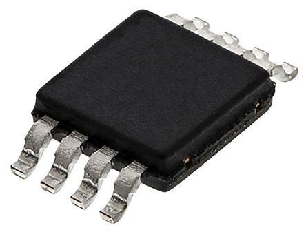
| 产品图片 |
|
| rohs | 符合RoHS无铅 / 符合限制有害物质指令(RoHS)规范要求 |
| 产品系列 | 校验器 IC,Texas Instruments TLV3702IDGK- |
| 数据手册 | |
| 产品型号 | TLV3702IDGK |
| PCN设计/规格 | |
| 产品 | Analog Comparators |
| 产品目录页面 | |
| 产品种类 | 模拟比较器 |
| 传播延迟(最大值) | - |
| 供应商器件封装 | 8-VSSOP |
| 偏转电压—最大值 | 5 mV |
| 元件数 | 2 |
| 其它名称 | 296-12610-5 |
| 包装 | 管件 |
| 单位重量 | 19 mg |
| 响应时间 | 36 us |
| 商标 | Texas Instruments |
| 安装类型 | 表面贴装 |
| 安装风格 | SMD/SMT |
| 封装 | Tube |
| 封装/外壳 | 8-TSSOP,8-MSOP(0.118",3.00mm 宽) |
| 封装/箱体 | VSSOP-8 |
| 工作温度 | -40°C ~ 125°C |
| 工厂包装数量 | 80 |
| 最大功率耗散 | 481 mW |
| 最大工作温度 | + 125 C |
| 最小工作温度 | - 40 C |
| 标准包装 | 80 |
| 比较器类型 | General Purpose |
| 滞后 | - |
| 电压-电源,单/双 (±) | 2.7 V ~ 16 V, ±1.35 V ~ 8 V |
| 电压-输入失调(最大值) | 5mV @ 15V |
| 电压增益dB | 120 dB |
| 电流-输入偏置(最大值) | 250pA @ 15V |
| 电流-输出(典型值) | 10mA |
| 电流-静态(最大值) | 1µA |
| 电源电压-最大 | 16 V |
| 电源电压-最小 | 2.7 V |
| 电源电流—最大值 | 800 nA |
| 类型 | 通用 |
| 系列 | TLV3702 |
| 输入偏压电流—最大 | 250 pA |
| 输出电流—典型值 | 10 mA |
| 输出类型 | CMOS,推挽式,满摆幅 |
| 通道数量 | 2 Channel |


- 商务部:美国ITC正式对集成电路等产品启动337调查
- 曝三星4nm工艺存在良率问题 高通将骁龙8 Gen1或转产台积电
- 太阳诱电将投资9.5亿元在常州建新厂生产MLCC 预计2023年完工
- 英特尔发布欧洲新工厂建设计划 深化IDM 2.0 战略
- 台积电先进制程称霸业界 有大客户加持明年业绩稳了
- 达到5530亿美元!SIA预计今年全球半导体销售额将创下新高
- 英特尔拟将自动驾驶子公司Mobileye上市 估值或超500亿美元
- 三星加码芯片和SET,合并消费电子和移动部门,撤换高东真等 CEO
- 三星电子宣布重大人事变动 还合并消费电子和移动部门
- 海关总署:前11个月进口集成电路产品价值2.52万亿元 增长14.8%


PDF Datasheet 数据手册内容提取
Product Order Technical Tools & Support & Folder Now Documents Software Community TLV3701,TLV3702,TLV3704 SLCS137D–NOVEMBER2000–REVISEDMAY2017 TLV370x Family of Nanopower, Push-Pull Output Comparators 1 Features 3 Description • LowSupplyCurrent...560nA/PerChannel The TLV370x is Texas Instruments’ first family of 1 nanopower comparators with only 560 nA per • InputCommon-ModeRangeExceedstheRails... channel supply current, which make this device ideal –0.1VtoV +5V CC forbatterypowerandwirelesshandsetapplications. • SupplyVoltageRange...2.5Vto16V The TLV370x has a minimum operating supply • ReverseBatteryProtectionUpto18V voltage of 2.7 V over the extended industrial • Push-PullCMOSOutputStage temperature range (T = –40°C to 125°C), while A having an input common-mode range of –0.1 to V • SpecifiedTemperatureRange CC + 5 V. The low supply current makes it an ideal – 0°Cto70°C–CommercialGrade choice for battery-powered portable applications – –40°Cto125°C –IndustrialGrade where quiescent current is the primary concern. • Ultra-SmallPackaging Reverse battery protection guards the amplifier from an overcurrent condition due to improper battery – 5-PinSOT-23(TLV3701) installation. For harsh environments, the inputs can – 8-PinMSOP(TLV3702) be taken 5 V above the positive supply rail without • UniversalOp-AmpEVM(ReferenceSLOU060for damagetothedevice. MoreInformation) All members are available in PDIP and SOIC with the singles in the small SOT-23 package, duals in the 2 Applications MSOP,andquadsintheTSSOPpackage. • PortableBatteryMonitoring DeviceInformation(1) • ConsumerMedicalElectronics PARTNUMBER PACKAGE BODYSIZE(NOM) • SecurityDetectionSystems SOT-23(5) 2.90mm×1.60mm • HandheldInstruments TLV3701 SOIC(8) 4.90mm×3.91mm • Ultra-LowPowerSystems SOIC(8) 4.90mm×3.91mm TLV3702 VSSOP(8) 3.00mm×3.00mm PDIP(8) 9.81mm×6.35mm SOIC(14) 8.65mm×3.91mm TLV3704 PDIP(14) 19.30mm×6.35mm TSSOP(14) 5.00mm×4.40mm (1) For all available packages, see the orderable addendum at theendofthedatasheet. SupplyCurrentvsSupplyVoltage High-SideVoltageSenseCircuit 800 TA=125°C R1 R3 700 1MΩ 100kΩ nA TA=70°C h– 600 TA=25°C VCC+ C TLV370X urrent/ 500 1MRΩ2 Vref µP yC 400 TA=0°C ppl TA=–40°C 0 D1 u S 300 – C C I 200 0 VID=–1V 100 Copyright © 2016,Texas Instruments Incorporated 0 2 4 6 8 10 12 14 16 VCC–SupplyVoltage–V 1 An IMPORTANT NOTICE at the end of this data sheet addresses availability, warranty, changes, use in safety-critical applications, intellectualpropertymattersandotherimportantdisclaimers.PRODUCTIONDATA.
TLV3701,TLV3702,TLV3704 SLCS137D–NOVEMBER2000–REVISEDMAY2017 www.ti.com Table of Contents 1 Features.................................................................. 1 8.3 FeatureDescription.................................................13 2 Applications........................................................... 1 8.4 DeviceFunctionalModes........................................13 3 Description............................................................. 1 9 ApplicationandImplementation........................ 14 4 RevisionHistory..................................................... 2 9.1 ApplicationInformation............................................14 9.2 TypicalApplication .................................................14 5 DeviceComparisonTables................................... 3 10 PowerSupplyRecommendations..................... 16 6 PinConfigurationandFunctions......................... 4 11 Layout................................................................... 16 7 Specifications......................................................... 6 11.1 LayoutGuidelines.................................................16 7.1 AbsoluteMaximumRatings......................................6 11.2 LayoutExample....................................................16 7.2 RecommendedOperatingConditions.......................6 12 DeviceandDocumentationSupport................. 17 7.3 ThermalInformation–TLV3701...............................7 7.4 ThermalInformation–TLV3702...............................7 12.1 DeviceSupport......................................................17 7.5 ThermalInformation–TLV3704...............................7 12.2 DocumentationSupport .......................................17 7.6 ElectricalCharacteristics...........................................8 12.3 RelatedLinks........................................................17 7.7 SwitchingCharacteristics..........................................9 12.4 ReceivingNotificationofDocumentationUpdates17 7.8 DissipationRatings...................................................9 12.5 CommunityResources..........................................18 7.9 TypicalCharacteristics............................................10 12.6 Trademarks...........................................................18 12.7 ElectrostaticDischargeCaution............................18 8 DetailedDescription............................................ 13 12.8 Glossary................................................................18 8.1 Overview.................................................................13 13 Mechanical,Packaging,andOrderable 8.2 FunctionalBlockDiagram.......................................13 Information........................................................... 18 4 Revision History ChangesfromRevisionC(March2017)toRevisionD Page • ChangedWordingofStart-uptimetablenote ....................................................................................................................... 9 ChangesfromRevisionB(August2001)toRevisionC Page • AddedDeviceInformationtable,DeviceComparisontable,ESDRatingstable,FeatureDescriptionsection,Device FunctionalModes,ApplicationandImplementationsection,PowerSupplyRecommendationssection,Layout section,DeviceandDocumentationSupportsection,andMechanical,Packaging,andOrderableInformationsection......1 • ChangedVOHtypicalvaluefrom0.08to80toreflectproperunits....................................................................................... 8 • ChangedDissapationRatingsTabletoreflectnewpackagethermals.................................................................................. 9 • Deletedextraneous"OpenCollectorLeakage"graph.......................................................................................................... 10 2 SubmitDocumentationFeedback Copyright©2000–2017,TexasInstrumentsIncorporated ProductFolderLinks:TLV3701 TLV3702 TLV3704
TLV3701,TLV3702,TLV3704 www.ti.com SLCS137D–NOVEMBER2000–REVISEDMAY2017 5 Device Comparison Tables Table1.SelectionofComparators(1) OUTP RAIL- UT DEVICE VCC(V) VIO(µV) ICC/Ch(µA) IIB(pA) tPLH(µs) tPHL(μs) tf(μs) tr(μs) TO- STAG RAIL E TLV370x 2.5–16 250 0.56 80 56 83 22 8 I PP TLV340x 2.5–16 250 0.47 80 55 30 5 — I OD TLC3702/4 3–16 1200 9 5 1.1 0.65 0.5 0.125 — PP TLC393/339 3–16 1400 11 5 1.1 0.55 0.22 — — OD TLC372/4 3–16 1000 75 5 0.65 0.65 — — — OD (1) Allspecificationsaretypicalvaluesmeasuredat5V. Table2.TLV3701AvailableOptions PACKAGEDDEVICES T V maxAT25°C A IO SMALLOUTLINE(D)(1) SOT-23(DBV)(2) SYMBOL PLASTICDIP(P) 0°Cto70°C TLV3701CD TLV3701CDBV VBCC — 5000µV –40°Cto125°C TLV3701ID TLV3701IDBV VBCI TLV3701IP (1) Thispackageisavailabletapedandreeled.Toorderthispackagingoption,addanRsuffixtothepartnumber(forexample, TLV3701CDR). (2) Thispackageisonlyavailabletapedandreeled.Forstandardquantities(3000piecesperreel),addanRsuffix(thatis,TLV3701 CDBVR).Forsmallquantities(250piecespermini-reel),addaTsuffixtothepartnumber(forexample,TLV3701CDBVT). Table3.TLV3702AvailableOptions PACKAGEDDEVICES T V maxAT25°C A IO SMALLOUTLINE(D)(1) MSOP(DGK) SYMBOL PLASTICDIP(P) 0°Cto70°C TLV3702CD TLV3702CDGK xxTIAKC — 5000µV –40°Cto125°C TLV3702ID TLV3702IDGK xxTIAKD TLV3702IP (1) Thispackageisavailabletapedandreeled.Toorderthispackagingoption,addanRsuffixtothepartnumber(forexample, TLV3702CDR). Table4.TLV3704AvailableOptions PACKAGEDDEVICES T V maxAT25°C A IO SMALLOUTLINE(D)(1) PLASTICDIP(N) TSSOP(PW) 0°Cto70°C TLV3704CD — TLV3704CPW 5000µV –40°Cto125°C TLV3704ID TLV3704IN TLV3704IPW (1) Thispackageisavailabletapedandreeled.Toorderthispackagingoption,addanRsuffixtothepartnumber(forexample, TLV3704CDR). Copyright©2000–2017,TexasInstrumentsIncorporated SubmitDocumentationFeedback 3 ProductFolderLinks:TLV3701 TLV3702 TLV3704
TLV3701,TLV3702,TLV3704 SLCS137D–NOVEMBER2000–REVISEDMAY2017 www.ti.com 6 Pin Configuration and Functions TLV3701DBVPackage TLV3701DorPPackage 5-PinSOT-23 8-PinSOICorPDIP TopView TopView OUT 1 5 VCC NC 1 8 NC IN- 2 7 VCC GND 2 IN+ 3 6 OUT GND 4 5 NC IN+ 3 4 IN- TLV3701PinFunctions PIN I/O DESCRIPTION NAME SOT-23 SOIC,PDIP GND 2 4 — Ground IN– 4 2 I Negative(inverting)input IN+ 3 3 I Positive(noninverting)input NC — 1,5,8 — Nointernalconnection(canbeleftfloating) OUT 1 6 O Output V 5 7 — Positivepowersupply CC TLV3702D,DGK,orPPackage 8-PinSOIC,VSSOP,orPDIP TopView 1OUT 1 8 VCC 1IN- 2 7 2OUT 1IN+ 3 6 2IN- GND 4 5 2IN+ TLV3702PinFunctions PIN I/O DESCRIPTION NAME NO. GND 4 — Ground 1IN– 2 I Invertinginput,channel1 2IN– 6 I Invertinginput,channel2 1IN+ 3 I Noninvertinginput,channel1 2IN+ 5 I Noninvertinginput,channel2 1OUT 1 O Output,channel1 2OUT 7 O Output,channel2 V 8 — Positivepowersupply CC 4 SubmitDocumentationFeedback Copyright©2000–2017,TexasInstrumentsIncorporated ProductFolderLinks:TLV3701 TLV3702 TLV3704
TLV3701,TLV3702,TLV3704 www.ti.com SLCS137D–NOVEMBER2000–REVISEDMAY2017 TLV3704D,N,orPWPackage 14-PinSOIC,PDIP,orTSSOP TopView 1OUT 1 14 4OUT 1IN- 2 13 4IN- 1IN+ 3 12 4IN+ VCC 4 11 GND 2IN+ 5 10 3IN+ 2IN- 6 9 3IN- 2OUT 7 8 3OUT TLV3704PinFunctions PIN I/O DESCRIPTION NAME NO. GND 11 — Ground 1IN– 2 I Invertinginput,channel1 2IN– 6 I Invertinginput,channel2 3IN– 9 I Invertinginput,channel3 4IN– 13 I Invertinginput,channel4 1IN+ 3 I Noninvertinginput,channel1 2IN+ 5 I Noninvertinginput,channel2 3IN+ 10 I Noninvertinginput,channel3 4IN+ 12 I Noninvertinginput,channel4 1OUT 1 O Output,channel1 2OUT 7 O Output,channel2 3OUT 8 O Output,channel3 4OUT 14 O Output,channel4 V 4 — Positivepowersupply CC Copyright©2000–2017,TexasInstrumentsIncorporated SubmitDocumentationFeedback 5 ProductFolderLinks:TLV3701 TLV3702 TLV3704
TLV3701,TLV3702,TLV3704 SLCS137D–NOVEMBER2000–REVISEDMAY2017 www.ti.com 7 Specifications 7.1 Absolute Maximum Ratings overoperatingfree-airtemperaturerange(unlessotherwisenoted)(1) MIN MAX UNIT Supplyvoltage,V (2) 17 V CC Differentialinputvoltage,V ±20 V ID Inputvoltage,V(2)(3) 0 V +5 V I CC Inputcurrent,I ±10 mA I Outputcurrent,I ±10 mA O Continuoustotalpowerdissipation SeeDissipationRatings Maximumjunctiontemperature,T 150 °C J Leadtemperature1,6mm(1/16inch)fromcasefor10seconds 260 °C Storagetemperature,T –65 150 °C stg (1) StressesbeyondthoselistedunderAbsoluteMaximumRatingsmaycausepermanentdamagetothedevice.Thesearestressratings only,whichdonotimplyfunctionaloperationofthedeviceattheseoranyotherconditionsbeyondthoseindicatedunderRecommended OperatingConditions.Exposuretoabsolute-maximum-ratedconditionsforextendedperiodsmayaffectdevicereliability. (2) Allvoltagevalues,exceptdifferentialvoltages,arewithrespecttoGND. (3) Inputvoltagerangeislimitedto20VmaximumorV +5V,whicheverissmaller. CC 7.2 Recommended Operating Conditions overoperatingfree-airtemperaturerange(unlessotherwisenoted) MIN MAX UNIT C-suffix 2.5 16 Singlesupply I-suffix 2.7 16 Supplyvoltage,V V CC C-suffix ±1.25 ±8 Splitsupply I-suffix ±1.35 ±8 Common-modeinputvoltage,V –0.1 V +5 V ICR CC C-suffix 0 70 Operatingfree-airtemperature,T °C A I-suffix –40 125 6 SubmitDocumentationFeedback Copyright©2000–2017,TexasInstrumentsIncorporated ProductFolderLinks:TLV3701 TLV3702 TLV3704
TLV3701,TLV3702,TLV3704 www.ti.com SLCS137D–NOVEMBER2000–REVISEDMAY2017 7.3 Thermal Information – TLV3701 TLV3701 THERMALMETRIC(1) DBV(SOT-23) D(SOIC) P(PDIP) UNIT 5PINS 8PINS R Junction-to-ambientthermalresistance 193.6 124.8 82.8 °C/W θJA R Junction-to-case(top)thermalresistance 102.4 69.1 84.8 °C/W θJC(top) R Junction-to-boardthermalresistance 54.3 67.9 59.7 °C/W θJB ψ Junction-to-topcharacterizationparameter 16.9 22.3 45.3 °C/W JT ψ Junction-to-boardcharacterizationparameter 53.6 67.2 59.5 °C/W JB R Junction-to-case(bottom)thermalresistance — — — °C/W θJC(bot) (1) Formoreinformationabouttraditionalandnewthermalmetrics,seetheSemiconductorandICPackageThermalMetricsapplication report. 7.4 Thermal Information – TLV3702 TLV3702 THERMALMETRIC(1) D(SOIC) DGK(VSSOP) P(PDIP) UNIT 8PINS R Junction-to-ambientthermalresistance 116.7 163.9 77.1 °C/W θJA R Junction-to-case(top)thermalresistance 59.4 65.7 79 °C/W θJC(top) R Junction-to-boardthermalresistance 60.2 85.3 54 °C/W θJB ψ Junction-to-topcharacterizationparameter 14.6 9 39.5 °C/W JT ψ Junction-to-boardcharacterizationparameter 59.5 83.9 53.7 °C/W JB R Junction-to-case(bottom)thermalresistance — — — °C/W θJC(bot) (1) Formoreinformationabouttraditionalandnewthermalmetrics,seetheSemiconductorandICPackageThermalMetricsapplication report. 7.5 Thermal Information – TLV3704 TLV3704 THERMALMETRIC(1) D(SOIC) N(PDIP) PW(TSSOP) UNIT 14PINS R Junction-to-ambientthermalresistance 81.4 58.1 105.7 °C/W θJA R Junction-to-case(top)thermalresistance 38.1 50.9 33.9 °C/W θJC(top) R Junction-to-boardthermalresistance 37.8 38 49.5 °C/W θJB ψ Junction-to-topcharacterizationparameter 7.5 23.6 2.5 °C/W JT ψ Junction-to-boardcharacterizationparameter 37.4 37.7 48.8 °C/W JB R Junction-to-case(bottom)thermalresistance — — — °C/W θJC(bot) (1) Formoreinformationabouttraditionalandnewthermalmetrics,seetheSemiconductorandICPackageThermalMetricsapplication report. Copyright©2000–2017,TexasInstrumentsIncorporated SubmitDocumentationFeedback 7 ProductFolderLinks:TLV3701 TLV3702 TLV3704
TLV3701,TLV3702,TLV3704 SLCS137D–NOVEMBER2000–REVISEDMAY2017 www.ti.com 7.6 Electrical Characteristics Atspecifiedoperatingfree-airtemperaturerange,V =2.7V,5V,15V(unlessotherwisenoted). CC PARAMETER TESTCONDITIONS T (1) MIN TYP MAX UNIT A DCPERFORMANCE 25°C 250 5000 V Inputoffsetvoltage V =V /2,R =50Ω µV IO IC CC S Fullrange 7000 α Offsetvoltagedrift V =V /2,R =50Ω 25°C 3 µV/°C VIO IC CC S 25°C 55 72 V =0to2.7V,R =50Ω IC S Fullrange 50 25°C 60 76 CMRR Common-moderejectionratio V =0to5V,R =50Ω dB IC S Fullrange 55 25°C 65 88 V =0to15V,R =50Ω IC S Fullrange 60 Large-signaldifferentialvoltage A 25°C 1000 V/mV VD amplification INPUT/OUTPUTCHARACTERISTICS 25°C 20 100 I Inputoffsetcurrent V =V /2,R =50Ω pA IO IC CC S Fullrange 1000 25°C 80 250 I Inputbiascurrent V =V /2,R =50Ω pA IB IC CC S Fullrange 1500 r Differentialinputresistance 25°C 300 MΩ i(d) V – V =V /2,I =2μA,V =1V 25°C CC IC CC OH ID 80 V – V High-leveloutputvoltage 25°C CC mV OH 320 V =V /2,I =–50μA,V =1V IC CC OH ID V – Fullrange CC 450 V =V /2,I =2μA,V =–1V 25°C 8 IC CC OH ID V Low-leveloutputvoltage 25°C 80 200 mV OL V =V /2,I =50μA,V =–1V IC CC OH ID Fullrange 300 POWERSUPPLY 25°C 560 800 I Supplycurrent(perchannel) Outputstatehigh nA CC Fullrange 1000 25°C 75 100 V =2.7Vto5V CC V =V /2V,No Fullrange 70 PSRR Powersupplyrejectionratio IC CC dB load 25°C 85 105 V =5Vto15V CC Fullrange 80 (1) Fullrangeis0°Cto70°CforCsuffixand–40°Cto125°CforIsuffix.Ifnotspecified,fullrangeis–40°Cto125°C. 8 SubmitDocumentationFeedback Copyright©2000–2017,TexasInstrumentsIncorporated ProductFolderLinks:TLV3701 TLV3702 TLV3704
TLV3701,TLV3702,TLV3704 www.ti.com SLCS137D–NOVEMBER2000–REVISEDMAY2017 7.7 Switching Characteristics Atspecifiedoperatingfree-airtemperaturerange,V =2.7V,5V,15V(unlessotherwisenoted). CC PARAMETER TESTCONDITIONS MIN TYP MAX UNIT Overdrive=2mV 240 f=10kHz,V =100 Propagationresponsetime, STEP t(PLH) low-to-high-leveloutput(1) mV,CL=10pF,VCC=2.7 Overdrive=10mV 64 µs V Overdrive=50mV 36 Overdrive=2mV 167 f=10kHz,V =100 Propagationresponsetime, STEP t(PHL) high-to-low-leveloutput(1) mV,CL=10pF,VCC=2.7 Overdrive=10mV 67 µs V Overdrive=50mV 37 t Risetime C =10pF,V =2.7V 7 µs r L CC t Falltime C =10pF,V =2.7V 9 µs f L CC 25°C 7 15 t Start-uptime(TLV3701Only) V =2.7to15V(2) ms su CC Fullrange 14 30 (1) Theresponsetimespecifiedistheintervalbetweentheinputstepfunctionandtheinstantwhentheoutputcrosses1.4V.Propagation responsesarelongerathighersupplyvoltages,refertoFigures12–17forfurtherdetails. (2) Thedefinitionofstart-uptimeisthetimeperiodbetweenthesupplyvoltagereachingminimumsupply(V )andthedeviceIQ CCmin activating(I )withavaliddeviceoutputvoltage.Singledeviceonly. CCmin 7.8 Dissipation Ratings PACKAGE θ (°C/W) θ (°C/W) T ≤25°CPOWERRATING T =125°CPOWER JC JA A A RATING D(8) 69.1 124.8 1001mW 200mW D(14) 38.1 81.4 1536mW 307mW DBV(5) 102.4 193.6 646mW 129mW DGK(8) 65.7 163.9 763mW 153mW N(14) 50.9 58.1 2151mW 430mW P(8) 84.8 82.8 1510mW 302mW PW(14) 33.9 105.7 1183mW 237mW Copyright©2000–2017,TexasInstrumentsIncorporated SubmitDocumentationFeedback 9 ProductFolderLinks:TLV3701 TLV3702 TLV3704
TLV3701,TLV3702,TLV3704 SLCS137D–NOVEMBER2000–REVISEDMAY2017 www.ti.com 7.9 Typical Characteristics Atspecifiedoperatingconditions(unlessotherwisenoted). Table5.TableofGraphs FIGURE Inputbias/offsetcurrent vsFree-airtemperature Figure2 V Low-leveloutputvoltage vsLow-leveloutputcurrent Figure6,Figure8,Figure4 OL V High-leveloutputvoltage vsHigh-leveloutputcurrent Figure3,Figure5,Figure7 OH vsSupplyvoltage Figure1 I Supplycurrent CC Free-airtemperature Figure9 Outputfalltime/risetime vsSupplyvoltage Figure10 Low-to-highleveloutputresponseforvariousinputoverdrives Figure11,Figure13,Figure15 High-to-lowleveloutputresponseforvariousinputoverdrives Figure12,Figure14,Figure16 800 1200 TA=125°C A VCC =15V p 700 –1000 nA TA=70°C ent –h 600 TA=25°C Curr 800 C yCurrent/ 450000 TA=0°C Bias/Offset 460000 IIB ppl TA=–40°C ut u p –S 300 –In 200 C O IIO IC 200 II 0 / VID=–1V IIB 100 –200 0 2 4 6 8 10 12 14 16 –40–25 –10 5 20 35 50 65 80 95 110125 VCC–SupplyVoltage–V TA –Free-AirTemperature–°C Figure1.SupplyCurrentvsSupplyVoltage Figure2.InputBias/OffsetCurrentvsFree-AirTemperature 2.7 2.7 VCC =2.7V VCC=2.7V 2.4 VID =–1V 2.4 VID=–1V V V TA=125°C Voltage– 12..81 TA=T–A4=0°0C°C Voltage– 12..81 TTAA==2750°°CC Output 11..25 TA=25°C Output 11..25 High-Level 00..69 TA=70°C Low-Level 00..69 TA=T–A40=°0C°C – – H0.3 L0.3 VO TA=125°C VO 0.0 0.0 0 0.05 0.1 0.15 0.2 0.25 0.3 0.35 0.4 0.45 0 0.1 0.2 0.3 0.4 0.5 0.6 0.7 0.8 IOH –High-LevelOutputCurrent–mA IOL–Low-LevelOutputCurrent–mA Figure3.High-LevelOutputVoltagevsHigh-LevelOutput Figure4.Low-LevelOutputVoltagevsLow-LevelOutput Current Current 10 SubmitDocumentationFeedback Copyright©2000–2017,TexasInstrumentsIncorporated ProductFolderLinks:TLV3701 TLV3702 TLV3704
TLV3701,TLV3702,TLV3704 www.ti.com SLCS137D–NOVEMBER2000–REVISEDMAY2017 5 5 VCC=5V VCC =5V 4.5 VID=–1V 4.5 VID =–1V V 4 V 4 OutputVoltage- 23..355 TA=25°C TA=–4T0A°=C0°C OutputVoltage– 23..355 TA=TA70=°1C25°C High-Level 1.215 TA=70°C Low-Level 1.215 TA=TA0=°C25°C –OH0.5 TA=125°C –OL0.5 TA=–40°C V V 0 0 0 0.2 0.4 0.6 0.8 1.0 1.2 1.4 1.6 1.8 0 0.4 0.8 1.2 1.6 2.0 2.4 2.8 IOH–High-LevelOutputCurrent–mA IOL–Low-LevelOutputCurrent–mA Figure5.High-LevelOutputVoltagevsHigh-LevelOutput Figure6.Low-LevelOutputVoltagevsLow-LevelOutput Current Current 15 15 TA=0°C VCC=15V 13.5 13.5 VID=–1V OutputVoltage–V1071..2955 TA=25°C TA=–40°C OutputVoltage-V1071..2955 TTAA==T27A50=°°CC125°C gh-Level 4.65 TA=70°C w-Level 4.65 –Hi 3 TA=125°C Lo– 3 TA=0°C OH 1.5 VCC=15V OL 1.5 TA=–40°C V VID=–1V V 0 0 0 1 2 3 4 5 6 7 8 9 0 1 2 3 4 5 6 7 8 9 IOH–High-LevelOutputCurrent–mA IOL–Low-LevelOutputCurrent– mA Figure7.High-LevelOutputVoltagevsHigh-LevelOutput Figure8.Low-LevelOutputVoltagevsLow-LevelOutput Current Current 700 120 VCC=2.7V,5V,15V VID=1Vto–1V 600 VID=–1V s InputRise/FallTime=4µs µ–100 CL=10pF A e TA=25°C n 500 m h– Ti 80 urrent/C 400 Rise/Fall 60 FallTime C 300 ut y p ppl Out 40 u 200 S – –CC100 tr(f) 20 I RiseTime 0 0 –40–25–10 5 20 35 50 65 80 95 110125 0 2.5 5 7.5 10 12.5 15 TA–Free-AirTemperature–°C VCC –SupplyVoltage–V Figure9.SupplyCurrentvsFree-AirTemperature Figure10.OutputRise/FallTimevsSupplyVoltage Copyright©2000–2017,TexasInstrumentsIncorporated SubmitDocumentationFeedback 11 ProductFolderLinks:TLV3701 TLV3702 TLV3704
TLV3701,TLV3702,TLV3704 SLCS137D–NOVEMBER2000–REVISEDMAY2017 www.ti.com 3 6 V2.7 V e–2.4 – 5 OutputVoltag001112......692581 105 0mmVV 2mV OutputVoltage 1234 1050mmVV 2mV –O0.3 – V 0 O 0 V 0.05 0.05 V 0 ntial–eV 0 ntial–ge VCTACLC==2=1502p.°7CFV –––000...110505 –VDiffereIDnputVoltag VCTACLC==21=505p°CVF –––000...110505 V–DiffereIDInputVolta 0 25 50 75 100125 150175200225250275300 I 0 25 50 75 100125150 175200 225250275300 t–Time –µs t–Time –µs Figure11.Low-to-HighOutputResponseforVariousInput Figure12.High-to-LowLevelOutputResponseforVarious Overdrives InputOverdrives 16 3 V 14 2.7 – V 2.4 Voltage 11028 50mV 2mV oltage– 112...581 50mV Output 46 10mV utputV 001...692 10mV 2mV –VO 02 –OO 0.03 V –0.3 VCC =15V 0.15 CTAL==2150p°CF –000.0.044 Differential–VoltageV VCTACLC==21=502p°.CF7V 00..0150 Differential–VoltageV ––00..1028 –VIDInput –00.05 V–IDInput 0 25 50 75 100 125150175200225250275300 0 25 50 75 100 125150 175200225250275300 t–Time –µs t–Time–µs Figure13.Low-to-HighLevelOutputResponseforVarious Figure14.High-to-LowLevelOutputResponseforVarious InputOverdrives InputOverdrives 6 16 V V 14 – 5 – e e 12 g 4 g Volta 3 50mV Volta 108 50mV 2mV put 2 10mV put 6 10mV ut ut 4 2mV O 1 O – – 2 O 0 O V V 0 V al V 0 25 50 75 1001251501752VCT0ACL0C=2=2215=5025p°5CVF0275300–0000..01.0505 –VDifferentialIDInput–Voltage 0 50 100 150 200 25VCT0ACLC3==0210=501p°35CF5V0 400–00000...001.04824 –DifferentiVIDInput–Voltage t–Time –µs t–Time –µs Figure15.Low-to-HighLevelOutputResponseforVarious Figure16.High-to-LowLevelOutputResponseforVarious InputOverdrives InputOverdrives 12 SubmitDocumentationFeedback Copyright©2000–2017,TexasInstrumentsIncorporated ProductFolderLinks:TLV3701 TLV3702 TLV3704
TLV3701,TLV3702,TLV3704 www.ti.com SLCS137D–NOVEMBER2000–REVISEDMAY2017 8 Detailed Description 8.1 Overview The TLV370x is a family of nanopower comparators drawing only 560 nA per channel supply current. Having a minimum operating supply voltage of 2.7 V over the extended industrial temperature range (T = –40°C to A +125°C), while having an input common-mode range of –0.1 to V + 5 V makes this device ideal for battery- CC poweredandwirelesshandsetapplications. 8.2 Functional Block Diagram VCC IN+ OUT IN– GND Copyright © 2016, Texas Instruments Incorporated 8.3 Feature Description 8.3.1 OperatingVoltage The TLV340x comparators are specified for use on a single supply from 2.5 V to 16 V (or a dual supply from ±1.25Vto ±16V)overatemperaturerangeof −40°Cto+125°C. 8.3.2 SettingtheThreshold Using a low-power, stable reference is important when setting the transition point for the TLV340x devices. The REF3312, as shown in Figure 17, provides a 1.25-V reference voltage with low drift and only 3.9 µA of quiescent current. VS Input voltage IN+ VCC Output voltage OUT VS REF3312 IN– GND 1.25 V threshold voltage Copyright © 2016, Texas Instruments Incorporated Figure17. SettingtheThreshold 8.4 Device Functional Modes The TLV370x has a single functional mode and is operational when the power supply voltage applied ranges from2.5V(±1.25V)to16V(±8V). Copyright©2000–2017,TexasInstrumentsIncorporated SubmitDocumentationFeedback 13 ProductFolderLinks:TLV3701 TLV3702 TLV3704
TLV3701,TLV3702,TLV3704 SLCS137D–NOVEMBER2000–REVISEDMAY2017 www.ti.com 9 Application and Implementation NOTE Information in the following applications sections is not part of the TI component specification, and TI does not warrant its accuracy or completeness. TI’s customers are responsible for determining suitability of components for their purposes. Customers should validateandtesttheirdesignimplementationtoconfirmsystemfunctionality. 9.1 Application Information Manyapplicationsrequirethedetectionofasignal(voltageorcurrent)thatexceedsaparticularthresholdvoltage or current. Using a comparator to make that threshold detection is the easiest, lowest power and highest speed waytomakeathresholddetection. 9.2 Typical Application 5 V Input voltage IN+ VCC Output voltage OUT 5 V REF3312 IN– GND 1.25 V threshold voltage Copyright © 2016, Texas Instruments Incorporated Figure18. 1.25-VThresholdDetector 9.2.1 DesignRequirements • Detectwhenasignalisaboveorbelow1.25V • Operatefromasingle5-Vpowersupply • Rail-to-railinputvoltagerangefrom0to5V • Rail-to-railoutputvoltagerangefrom0to5V 9.2.2 DetailedDesignProcedure The input voltage range in the circuit illustrated in Figure 18 is limited only by the power supply applied to the TV3701.Inthisexamplewiththeselectionofa5-V,single-supplypowersupply,theinputvoltagerangeislimited to 0 to V + 5 V, or 0 to 10 V. The threshold voltage of 1.25 V can de derived in a variety of ways. As the S TLV3701 is a very low-power device, it is desirable to also use very low power to create the threshold voltage. The REF3312 series voltage reference is selected for its stable output voltage of 1.25 V and its low power consumption of only 3.9 µA. The TLV3701 is an push-pull output comparator, and does not require a pullup resistortosavepower. 14 SubmitDocumentationFeedback Copyright©2000–2017,TexasInstrumentsIncorporated ProductFolderLinks:TLV3701 TLV3702 TLV3704
TLV3701,TLV3702,TLV3704 www.ti.com SLCS137D–NOVEMBER2000–REVISEDMAY2017 Typical Application (continued) 9.2.3 ApplicationCurve 6 5 V) 4 e ( g a olt 3 V ut p ut 2 O 1 0 0 1 2 3 4 5 Voltage at IN(cid:16) pin (V) Figure19. TransferFunctionfortheThresholdDetector Copyright©2000–2017,TexasInstrumentsIncorporated SubmitDocumentationFeedback 15 ProductFolderLinks:TLV3701 TLV3702 TLV3704
TLV3701,TLV3702,TLV3704 SLCS137D–NOVEMBER2000–REVISEDMAY2017 www.ti.com 10 Power Supply Recommendations The TLV340x device is specified for operation from 2.5 V to 16 V (±1.25 to ±8 V); many specifications apply from –40°C to +125°C. Parameters that can exhibit significant variance with regard to operating voltage or temperaturearepresentedinTypicalCharacteristics. 11 Layout 11.1 Layout Guidelines Figure 20 shows the typical connections for the TLV340x. To minimize supply noise, power supplies must be capacitively decoupled by a 0.01-µF ceramic capacitor in parallel with a 10-µF electrolytic capacitor. Comparators are very sensitive to input noise. Proper grounding (the use of a ground plane) helps to maintain thespecifiedperformanceoftheTLV340xfamily. Forbestresults,maintainthefollowinglayoutguidelines: 1. Useaprinted-circuitboard(PCB)withagood,unbrokenlow-inductancegroundplane. 2. Placeadecouplingcapacitor(0.1-µFceramic,surface-mountcapacitor)ascloseaspossibletoV . CC 3. On the inputs and the output, keep lead lengths as short as possible to avoid unwanted parasitic feedback aroundthecomparator.Keepinputsawayfromtheoutput. 4. SolderthedevicedirectlytothePCBratherthanusingasocket. 5. For slow-moving input signals, take care to prevent parasitic feedback. A small capacitor (1000 pF or less) placedbetweentheinputscanhelpeliminateoscillationsinthetransitionregion.Thiscapacitorcausessome degradation to propagation delay when the impedance is low. The top-side ground plane runs between the outputandinputs. 6. The ground pin ground trace runs under the device up to the bypass capacitor, shielding the inputs from the outputs. 11.2 Layout Example Power supply 0.01 µF 10 (cid:29)F V+ +IN OUT – IN OUT Power supply 1 5 0.01 µF 10 (cid:29)F 2 + – 3 4 Not to scale +IN –IN Copyright © 2016, Texas Instruments Incorporated Figure20. TLV3701SOT-23LayoutExample 16 SubmitDocumentationFeedback Copyright©2000–2017,TexasInstrumentsIncorporated ProductFolderLinks:TLV3701 TLV3702 TLV3704
TLV3701,TLV3702,TLV3704 www.ti.com SLCS137D–NOVEMBER2000–REVISEDMAY2017 12 Device and Documentation Support 12.1 Device Support 12.1.1 DevelopmentSupport 12.1.1.1 DIPAdapterEVM The DIP Adapter EVM tool provides an easy, low-cost way to prototype small surface mount ICs. The evaluation tool these TI packages: D or U (8-pin SOIC), PW (8-pin TSSOP), DGK (8-pin MSOP), DBV (6-pin SOT-23, 5-pin SOT23, and 3-pin SOT-23), DCK (6-pin SC-70 and 5-pin SC-70), and DRL (6-pin SOT-563). The DIP Adapter EVMmayalsobeusedwithterminalstripsormaybewireddirectlytoexistingcircuits. 12.1.1.2 UniversalOpAmpEVM The Universal Op Amp EVM is a series of general-purpose, blank circuit boards that simplify prototyping circuits for a variety of IC package types. The evaluation module board design allows many different circuits to be constructed easily and quickly. Five models are offered, with each model intended for a specific package type. PDIP,SOIC,MSOP,TSSOP,andSOT-23packagesareallsupported. NOTE These boards are unpopulated, so users must provide their own ICs. TI recommends requestingseveralopampdevicesampleswhenorderingtheUniversalOpAmpEVM. 12.2 Documentation Support 12.2.1 RelatedDocumentation ThefollowingdocumentsarerelevantforusingtheTLV340xdevicesandarerecommendedforreference.Allare availablefordownloadatwww.ti.com(unlessotherwisenoted): • UniversalOpAmpEVMUserGuide (SLOU060) • HardwarePaceUsingSlopeDetection (SLAU511) • BipolarHigh-voltageDifferentialInterfaceforLow-VoltageComparators (TIDU039) • AC-CoupledSingleSupplyComparator (SLAU505) • ECGImplementationontheTMS320VC5505DSPMedicalDevelopmentKit (SPRAB36) • REF33xx3.9-μA,SC70-3,SOT-23-3,andUQFN-8,30-ppm/°CDriftVoltageReference(SBOS392) 12.3 Related Links The table below lists quick access links. Categories include technical documents, support and community resources,toolsandsoftware,andquickaccesstosampleorbuy. Table6.RelatedLinks TECHNICAL TOOLS& SUPPORT& PARTS PRODUCTFOLDER SAMPLE&BUY DOCUMENTS SOFTWARE COMMUNITY TLV3701 Clickhere Clickhere Clickhere Clickhere Clickhere TLV3702 Clickhere Clickhere Clickhere Clickhere Clickhere TLV3704 Clickhere Clickhere Clickhere Clickhere Clickhere 12.4 Receiving Notification of Documentation Updates To receive notification of documentation updates, navigate to the device product folder on ti.com. In the upper right corner, click on Alert me to register and receive a weekly digest of any product information that has changed.Forchangedetails,reviewtherevisionhistoryincludedinanyreviseddocument. Copyright©2000–2017,TexasInstrumentsIncorporated SubmitDocumentationFeedback 17 ProductFolderLinks:TLV3701 TLV3702 TLV3704
TLV3701,TLV3702,TLV3704 SLCS137D–NOVEMBER2000–REVISEDMAY2017 www.ti.com 12.5 Community Resources The following links connect to TI community resources. Linked contents are provided "AS IS" by the respective contributors. They do not constitute TI specifications and do not necessarily reflect TI's views; see TI's Terms of Use. TIE2E™OnlineCommunity TI'sEngineer-to-Engineer(E2E)Community.Createdtofostercollaboration amongengineers.Ate2e.ti.com,youcanaskquestions,shareknowledge,exploreideasandhelp solveproblemswithfellowengineers. DesignSupport TI'sDesignSupport QuicklyfindhelpfulE2Eforumsalongwithdesignsupporttoolsand contactinformationfortechnicalsupport. 12.6 Trademarks E2EisatrademarkofTexasInstruments. Allothertrademarksarethepropertyoftheirrespectiveowners. 12.7 Electrostatic Discharge Caution This integrated circuit can be damaged by ESD. Texas Instruments recommends that all integrated circuits be handled with appropriateprecautions.Failuretoobserveproperhandlingandinstallationprocedurescancausedamage. ESDdamagecanrangefromsubtleperformancedegradationtocompletedevicefailure.Precisionintegratedcircuitsmaybemore susceptibletodamagebecauseverysmallparametricchangescouldcausethedevicenottomeetitspublishedspecifications. 12.8 Glossary SLYZ022—TIGlossary. Thisglossarylistsandexplainsterms,acronyms,anddefinitions. 13 Mechanical, Packaging, and Orderable Information The following pages include mechanical, packaging, and orderable information. This information is the most current data available for the designated devices. This data is subject to change without notice and revision of thisdocument.Forbrowser-basedversionsofthisdatasheet,refertotheleft-handnavigation. 18 SubmitDocumentationFeedback Copyright©2000–2017,TexasInstrumentsIncorporated ProductFolderLinks:TLV3701 TLV3702 TLV3704
PACKAGE OPTION ADDENDUM www.ti.com 6-Feb-2020 PACKAGING INFORMATION Orderable Device Status Package Type Package Pins Package Eco Plan Lead/Ball Finish MSL Peak Temp Op Temp (°C) Device Marking Samples (1) Drawing Qty (2) (6) (3) (4/5) TLV3701CD ACTIVE SOIC D 8 75 Green (RoHS NIPDAU Level-1-260C-UNLIM 0 to 70 3701C & no Sb/Br) TLV3701CDBVR ACTIVE SOT-23 DBV 5 3000 Green (RoHS NIPDAU Level-1-260C-UNLIM 0 to 70 VBCC & no Sb/Br) TLV3701CDBVT ACTIVE SOT-23 DBV 5 250 Green (RoHS NIPDAU Level-1-260C-UNLIM 0 to 70 VBCC & no Sb/Br) TLV3701CDBVTG4 ACTIVE SOT-23 DBV 5 250 Green (RoHS NIPDAU Level-1-260C-UNLIM 0 to 70 VBCC & no Sb/Br) TLV3701ID ACTIVE SOIC D 8 75 Green (RoHS NIPDAU Level-1-260C-UNLIM -40 to 125 3701I & no Sb/Br) TLV3701IDBVR ACTIVE SOT-23 DBV 5 3000 Green (RoHS NIPDAU Level-1-260C-UNLIM -40 to 125 VBCI & no Sb/Br) TLV3701IDBVT ACTIVE SOT-23 DBV 5 250 Green (RoHS NIPDAU Level-1-260C-UNLIM -40 to 125 VBCI & no Sb/Br) TLV3701IDBVTG4 ACTIVE SOT-23 DBV 5 250 Green (RoHS NIPDAU Level-1-260C-UNLIM -40 to 125 VBCI & no Sb/Br) TLV3701IDR ACTIVE SOIC D 8 2500 Green (RoHS NIPDAU Level-1-260C-UNLIM -40 to 125 3701I & no Sb/Br) TLV3701IP ACTIVE PDIP P 8 50 Green (RoHS NIPDAU N / A for Pkg Type -40 to 125 TLV3701I & no Sb/Br) TLV3702CD ACTIVE SOIC D 8 75 Green (RoHS NIPDAU Level-1-260C-UNLIM 0 to 70 3702C & no Sb/Br) TLV3702CDGK ACTIVE VSSOP DGK 8 80 Green (RoHS NIPDAU Level-1-260C-UNLIM 0 to 70 AKC & no Sb/Br) TLV3702CDGKG4 ACTIVE VSSOP DGK 8 80 Green (RoHS NIPDAU Level-1-260C-UNLIM 0 to 70 AKC & no Sb/Br) TLV3702CDGKR ACTIVE VSSOP DGK 8 2500 Green (RoHS NIPDAU Level-1-260C-UNLIM 0 to 70 AKC & no Sb/Br) TLV3702CDGKRG4 ACTIVE VSSOP DGK 8 2500 Green (RoHS NIPDAU Level-1-260C-UNLIM 0 to 70 AKC & no Sb/Br) TLV3702ID ACTIVE SOIC D 8 75 Green (RoHS NIPDAU Level-1-260C-UNLIM -40 to 125 3702I & no Sb/Br) TLV3702IDGK ACTIVE VSSOP DGK 8 80 Green (RoHS NIPDAU Level-1-260C-UNLIM -40 to 125 AKD & no Sb/Br) Addendum-Page 1
PACKAGE OPTION ADDENDUM www.ti.com 6-Feb-2020 Orderable Device Status Package Type Package Pins Package Eco Plan Lead/Ball Finish MSL Peak Temp Op Temp (°C) Device Marking Samples (1) Drawing Qty (2) (6) (3) (4/5) TLV3702IDGKG4 ACTIVE VSSOP DGK 8 80 Green (RoHS NIPDAU Level-1-260C-UNLIM -40 to 125 AKD & no Sb/Br) TLV3702IDGKR ACTIVE VSSOP DGK 8 2500 Green (RoHS NIPDAU Level-1-260C-UNLIM -40 to 125 AKD & no Sb/Br) TLV3702IDGKRG4 ACTIVE VSSOP DGK 8 2500 Green (RoHS NIPDAU Level-1-260C-UNLIM -40 to 125 AKD & no Sb/Br) TLV3702IDR ACTIVE SOIC D 8 2500 Green (RoHS NIPDAU Level-1-260C-UNLIM -40 to 125 3702I & no Sb/Br) TLV3702IP ACTIVE PDIP P 8 50 Green (RoHS NIPDAU N / A for Pkg Type -40 to 125 TLV3702I & no Sb/Br) TLV3704CD ACTIVE SOIC D 14 50 Green (RoHS NIPDAU Level-1-260C-UNLIM 0 to 70 3704C & no Sb/Br) TLV3704CPW ACTIVE TSSOP PW 14 90 Green (RoHS NIPDAU Level-1-260C-UNLIM 0 to 70 3704C & no Sb/Br) TLV3704ID ACTIVE SOIC D 14 50 Green (RoHS NIPDAU Level-1-260C-UNLIM -40 to 125 3704I & no Sb/Br) TLV3704IDG4 ACTIVE SOIC D 14 50 Green (RoHS NIPDAU Level-1-260C-UNLIM -40 to 125 3704I & no Sb/Br) TLV3704IDR ACTIVE SOIC D 14 2500 Green (RoHS NIPDAU Level-1-260C-UNLIM -40 to 125 3704I & no Sb/Br) TLV3704IDRG4 ACTIVE SOIC D 14 2500 Green (RoHS NIPDAU Level-1-260C-UNLIM -40 to 125 3704I & no Sb/Br) TLV3704IN ACTIVE PDIP N 14 25 Green (RoHS NIPDAU N / A for Pkg Type -40 to 125 TLV3704I & no Sb/Br) TLV3704IPW ACTIVE TSSOP PW 14 90 Green (RoHS NIPDAU Level-1-260C-UNLIM -40 to 125 3704I & no Sb/Br) TLV3704IPWR ACTIVE TSSOP PW 14 2000 Green (RoHS NIPDAU Level-1-260C-UNLIM -40 to 125 3704I & no Sb/Br) TLV3704IPWRG4 ACTIVE TSSOP PW 14 2000 Green (RoHS NIPDAU Level-1-260C-UNLIM -40 to 125 3704I & no Sb/Br) (1) The marketing status values are defined as follows: ACTIVE: Product device recommended for new designs. LIFEBUY: TI has announced that the device will be discontinued, and a lifetime-buy period is in effect. NRND: Not recommended for new designs. Device is in production to support existing customers, but TI does not recommend using this part in a new design. PREVIEW: Device has been announced but is not in production. Samples may or may not be available. OBSOLETE: TI has discontinued the production of the device. Addendum-Page 2
PACKAGE OPTION ADDENDUM www.ti.com 6-Feb-2020 (2) RoHS: TI defines "RoHS" to mean semiconductor products that are compliant with the current EU RoHS requirements for all 10 RoHS substances, including the requirement that RoHS substance do not exceed 0.1% by weight in homogeneous materials. Where designed to be soldered at high temperatures, "RoHS" products are suitable for use in specified lead-free processes. TI may reference these types of products as "Pb-Free". RoHS Exempt: TI defines "RoHS Exempt" to mean products that contain lead but are compliant with EU RoHS pursuant to a specific EU RoHS exemption. Green: TI defines "Green" to mean the content of Chlorine (Cl) and Bromine (Br) based flame retardants meet JS709B low halogen requirements of <=1000ppm threshold. Antimony trioxide based flame retardants must also meet the <=1000ppm threshold requirement. (3) MSL, Peak Temp. - The Moisture Sensitivity Level rating according to the JEDEC industry standard classifications, and peak solder temperature. (4) There may be additional marking, which relates to the logo, the lot trace code information, or the environmental category on the device. (5) Multiple Device Markings will be inside parentheses. Only one Device Marking contained in parentheses and separated by a "~" will appear on a device. If a line is indented then it is a continuation of the previous line and the two combined represent the entire Device Marking for that device. (6) Lead/Ball Finish - Orderable Devices may have multiple material finish options. Finish options are separated by a vertical ruled line. Lead/Ball Finish values may wrap to two lines if the finish value exceeds the maximum column width. Important Information and Disclaimer:The information provided on this page represents TI's knowledge and belief as of the date that it is provided. TI bases its knowledge and belief on information provided by third parties, and makes no representation or warranty as to the accuracy of such information. Efforts are underway to better integrate information from third parties. TI has taken and continues to take reasonable steps to provide representative and accurate information but may not have conducted destructive testing or chemical analysis on incoming materials and chemicals. TI and TI suppliers consider certain information to be proprietary, and thus CAS numbers and other limited information may not be available for release. In no event shall TI's liability arising out of such information exceed the total purchase price of the TI part(s) at issue in this document sold by TI to Customer on an annual basis. OTHER QUALIFIED VERSIONS OF TLV3701, TLV3702 : •Automotive: TLV3701-Q1, TLV3702-Q1 •Enhanced Product: TLV3701-EP NOTE: Qualified Version Definitions: •Automotive - Q100 devices qualified for high-reliability automotive applications targeting zero defects •Enhanced Product - Supports Defense, Aerospace and Medical Applications Addendum-Page 3
PACKAGE MATERIALS INFORMATION www.ti.com 25-Sep-2019 TAPE AND REEL INFORMATION *Alldimensionsarenominal Device Package Package Pins SPQ Reel Reel A0 B0 K0 P1 W Pin1 Type Drawing Diameter Width (mm) (mm) (mm) (mm) (mm) Quadrant (mm) W1(mm) TLV3701CDBVR SOT-23 DBV 5 3000 180.0 9.0 3.15 3.2 1.4 4.0 8.0 Q3 TLV3701CDBVT SOT-23 DBV 5 250 180.0 9.0 3.15 3.2 1.4 4.0 8.0 Q3 TLV3701IDBVR SOT-23 DBV 5 3000 180.0 9.0 3.15 3.2 1.4 4.0 8.0 Q3 TLV3701IDBVT SOT-23 DBV 5 250 180.0 9.0 3.15 3.2 1.4 4.0 8.0 Q3 TLV3701IDR SOIC D 8 2500 330.0 12.4 6.4 5.2 2.1 8.0 12.0 Q1 TLV3702CDGKR VSSOP DGK 8 2500 330.0 12.4 5.3 3.4 1.4 8.0 12.0 Q1 TLV3702IDGKR VSSOP DGK 8 2500 330.0 12.4 5.3 3.4 1.4 8.0 12.0 Q1 TLV3702IDR SOIC D 8 2500 330.0 12.4 6.4 5.2 2.1 8.0 12.0 Q1 TLV3704IDR SOIC D 14 2500 330.0 16.4 6.5 9.0 2.1 8.0 16.0 Q1 TLV3704IPWR TSSOP PW 14 2000 330.0 12.4 6.9 5.6 1.6 8.0 12.0 Q1 PackMaterials-Page1
PACKAGE MATERIALS INFORMATION www.ti.com 25-Sep-2019 *Alldimensionsarenominal Device PackageType PackageDrawing Pins SPQ Length(mm) Width(mm) Height(mm) TLV3701CDBVR SOT-23 DBV 5 3000 182.0 182.0 20.0 TLV3701CDBVT SOT-23 DBV 5 250 182.0 182.0 20.0 TLV3701IDBVR SOT-23 DBV 5 3000 182.0 182.0 20.0 TLV3701IDBVT SOT-23 DBV 5 250 182.0 182.0 20.0 TLV3701IDR SOIC D 8 2500 340.5 338.1 20.6 TLV3702CDGKR VSSOP DGK 8 2500 358.0 335.0 35.0 TLV3702IDGKR VSSOP DGK 8 2500 358.0 335.0 35.0 TLV3702IDR SOIC D 8 2500 340.5 338.1 20.6 TLV3704IDR SOIC D 14 2500 333.2 345.9 28.6 TLV3704IPWR TSSOP PW 14 2000 367.0 367.0 35.0 PackMaterials-Page2
PACKAGE OUTLINE DBV0005A SOT-23 - 1.45 mm max height SCALE 4.000 SMALL OUTLINE TRANSISTOR C 3.0 2.6 0.1 C 1.75 1.45 1.45 B A 0.90 PIN 1 INDEX AREA 1 5 2X 0.95 3.05 2.75 1.9 1.9 2 4 3 0.5 5X 0.3 0.15 0.2 C A B (1.1) TYP 0.00 0.25 GAGE PLANE 0.22 TYP 0.08 8 TYP 0.6 0 0.3 TYP SEATING PLANE 4214839/E 09/2019 NOTES: 1. All linear dimensions are in millimeters. Any dimensions in parenthesis are for reference only. Dimensioning and tolerancing per ASME Y14.5M. 2. This drawing is subject to change without notice. 3. Refernce JEDEC MO-178. 4. Body dimensions do not include mold flash, protrusions, or gate burrs. Mold flash, protrusions, or gate burrs shall not exceed 0.15 mm per side. www.ti.com
EXAMPLE BOARD LAYOUT DBV0005A SOT-23 - 1.45 mm max height SMALL OUTLINE TRANSISTOR PKG 5X (1.1) 1 5 5X (0.6) SYMM (1.9) 2 2X (0.95) 3 4 (R0.05) TYP (2.6) LAND PATTERN EXAMPLE EXPOSED METAL SHOWN SCALE:15X SOLDER MASK SOLDER MASK METAL UNDER METAL OPENING OPENING SOLDER MASK EXPOSED METAL EXPOSED METAL 0.07 MAX 0.07 MIN ARROUND ARROUND NON SOLDER MASK SOLDER MASK DEFINED DEFINED (PREFERRED) SOLDER MASK DETAILS 4214839/E 09/2019 NOTES: (continued) 5. Publication IPC-7351 may have alternate designs. 6. Solder mask tolerances between and around signal pads can vary based on board fabrication site. www.ti.com
EXAMPLE STENCIL DESIGN DBV0005A SOT-23 - 1.45 mm max height SMALL OUTLINE TRANSISTOR PKG 5X (1.1) 1 5 5X (0.6) SYMM 2 (1.9) 2X(0.95) 3 4 (R0.05) TYP (2.6) SOLDER PASTE EXAMPLE BASED ON 0.125 mm THICK STENCIL SCALE:15X 4214839/E 09/2019 NOTES: (continued) 7. Laser cutting apertures with trapezoidal walls and rounded corners may offer better paste release. IPC-7525 may have alternate design recommendations. 8. Board assembly site may have different recommendations for stencil design. www.ti.com
None
None
None
None
PACKAGE OUTLINE D0008A SOIC - 1.75 mm max height SCALE 2.800 SMALL OUTLINE INTEGRATED CIRCUIT C SEATING PLANE .228-.244 TYP [5.80-6.19] .004 [0.1] C A PIN 1 ID AREA 6X .050 [1.27] 8 1 2X .189-.197 [4.81-5.00] .150 NOTE 3 [3.81] 4X (0 -15 ) 4 5 8X .012-.020 B .150-.157 [0.31-0.51] .069 MAX [3.81-3.98] .010 [0.25] C A B [1.75] NOTE 4 .005-.010 TYP [0.13-0.25] 4X (0 -15 ) SEE DETAIL A .010 [0.25] .004-.010 0 - 8 [0.11-0.25] .016-.050 [0.41-1.27] DETAIL A (.041) TYPICAL [1.04] 4214825/C 02/2019 NOTES: 1. Linear dimensions are in inches [millimeters]. Dimensions in parenthesis are for reference only. Controlling dimensions are in inches. Dimensioning and tolerancing per ASME Y14.5M. 2. This drawing is subject to change without notice. 3. This dimension does not include mold flash, protrusions, or gate burrs. Mold flash, protrusions, or gate burrs shall not exceed .006 [0.15] per side. 4. This dimension does not include interlead flash. 5. Reference JEDEC registration MS-012, variation AA. www.ti.com
EXAMPLE BOARD LAYOUT D0008A SOIC - 1.75 mm max height SMALL OUTLINE INTEGRATED CIRCUIT 8X (.061 ) [1.55] SYMM SEE DETAILS 1 8 8X (.024) [0.6] SYMM (R.002 ) TYP [0.05] 5 4 6X (.050 ) [1.27] (.213) [5.4] LAND PATTERN EXAMPLE EXPOSED METAL SHOWN SCALE:8X SOLDER MASK SOLDER MASK METAL OPENING OPENING METAL UNDER SOLDER MASK EXPOSED METAL EXPOSED METAL .0028 MAX .0028 MIN [0.07] [0.07] ALL AROUND ALL AROUND NON SOLDER MASK SOLDER MASK DEFINED DEFINED SOLDER MASK DETAILS 4214825/C 02/2019 NOTES: (continued) 6. Publication IPC-7351 may have alternate designs. 7. Solder mask tolerances between and around signal pads can vary based on board fabrication site. www.ti.com
EXAMPLE STENCIL DESIGN D0008A SOIC - 1.75 mm max height SMALL OUTLINE INTEGRATED CIRCUIT 8X (.061 ) [1.55] SYMM 1 8 8X (.024) [0.6] SYMM (R.002 ) TYP [0.05] 5 4 6X (.050 ) [1.27] (.213) [5.4] SOLDER PASTE EXAMPLE BASED ON .005 INCH [0.125 MM] THICK STENCIL SCALE:8X 4214825/C 02/2019 NOTES: (continued) 8. Laser cutting apertures with trapezoidal walls and rounded corners may offer better paste release. IPC-7525 may have alternate design recommendations. 9. Board assembly site may have different recommendations for stencil design. www.ti.com
None
None
None
None
IMPORTANTNOTICEANDDISCLAIMER TI PROVIDES TECHNICAL AND RELIABILITY DATA (INCLUDING DATASHEETS), DESIGN RESOURCES (INCLUDING REFERENCE DESIGNS), APPLICATION OR OTHER DESIGN ADVICE, WEB TOOLS, SAFETY INFORMATION, AND OTHER RESOURCES “AS IS” AND WITH ALL FAULTS, AND DISCLAIMS ALL WARRANTIES, EXPRESS AND IMPLIED, INCLUDING WITHOUT LIMITATION ANY IMPLIED WARRANTIES OF MERCHANTABILITY, FITNESS FOR A PARTICULAR PURPOSE OR NON-INFRINGEMENT OF THIRD PARTY INTELLECTUAL PROPERTY RIGHTS. These resources are intended for skilled developers designing with TI products. You are solely responsible for (1) selecting the appropriate TI products for your application, (2) designing, validating and testing your application, and (3) ensuring your application meets applicable standards, and any other safety, security, or other requirements. These resources are subject to change without notice. TI grants you permission to use these resources only for development of an application that uses the TI products described in the resource. Other reproduction and display of these resources is prohibited. No license is granted to any other TI intellectual property right or to any third party intellectual property right. TI disclaims responsibility for, and you will fully indemnify TI and its representatives against, any claims, damages, costs, losses, and liabilities arising out of your use of these resources. TI’s products are provided subject to TI’s Terms of Sale (www.ti.com/legal/termsofsale.html) or other applicable terms available either on ti.com or provided in conjunction with such TI products. TI’s provision of these resources does not expand or otherwise alter TI’s applicable warranties or warranty disclaimers for TI products. Mailing Address: Texas Instruments, Post Office Box 655303, Dallas, Texas 75265 Copyright © 2020, Texas Instruments Incorporated