 Datasheet下载
- 型号: TLV3401IDBVT
- 制造商: Texas Instruments
- 库位|库存: xxxx|xxxx
- 要求:
| 数量阶梯 | 香港交货 | 国内含税 |
| +xxxx | $xxxx | ¥xxxx |
查看当月历史价格
查看今年历史价格
TLV3401IDBVT产品简介:
ICGOO电子元器件商城为您提供TLV3401IDBVT由Texas Instruments设计生产,在icgoo商城现货销售,并且可以通过原厂、代理商等渠道进行代购。 TLV3401IDBVT价格参考¥19.44-¥30.66。Texas InstrumentsTLV3401IDBVT封装/规格:线性 - 比较器, 通用 比较器 CMOS,开路漏极 SOT-23-5。您可以下载TLV3401IDBVT参考资料、Datasheet数据手册功能说明书,资料中有TLV3401IDBVT 详细功能的应用电路图电压和使用方法及教程。
Texas Instruments的TLV3401IDBVT是一款超低功耗、单通道比较器,专为需要极低功耗的应用而设计。它的工作电压范围为1.6V至5.5V,静态电流仅为70nA(典型值),非常适合电池供电设备和便携式电子产品。

 应用场景:

1. 便携式医疗设备:
   TLV3401IDBVT的低功耗特性使其非常适合用于便携式医疗设备,如血糖仪、心率监测器和脉搏血氧仪等。这些设备通常依赖电池供电,且需要长时间工作而不频繁更换电池。TLV3401IDBVT的超低功耗可以显著延长设备的续航时间,同时其宽工作电压范围也适应了不同类型的电池。

2. 物联网(IoT)传感器节点:
   在物联网应用中,传感器节点通常部署在难以访问的位置,因此对功耗要求极为苛刻。TLV3401IDBVT可用于温度、湿度、压力等传感器的数据采集和处理,确保在低功耗模式下仍能准确触发报警或数据传输。其快速响应时间和低延迟特性也使得它能够及时捕捉到关键事件。

3. 智能家居设备:
   智能家居系统中的各种传感器和控制器,如烟雾探测器、门窗传感器、智能插座等,都可以使用TLV3401IDBVT来实现低功耗监控。例如,在烟雾探测器中,它可以用于检测烟雾浓度并触发警报,同时保持极低的待机功耗,以延长电池寿命。

4. 工业自动化:
   在工业环境中,许多传感器和控制系统需要长时间稳定运行。TLV3401IDBVT可以用于液位传感器、流量计等设备中,帮助实时监测生产过程中的关键参数。其高精度和可靠性确保了工业系统的稳定性和安全性。

5. 消费电子产品:
   对于手机、平板电脑等消费电子产品,TLV3401IDBVT可用于电池电量监测、充电状态检测等功能。它的低功耗特性不会对设备的整体功耗产生明显影响,同时提供了可靠的电压比较功能。

总之,TLV3401IDBVT凭借其超低功耗、宽工作电压范围和快速响应时间,广泛适用于各种对功耗敏感的应用场景,特别是在便携式设备和物联网领域表现尤为突出。
| 参数 | 数值 |
| 产品目录 | 集成电路 (IC)半导体 |
| CMRR,PSRR(典型值) | 88dB CMRR,105dB PSRR |
| 描述 | IC COMPARATOR SGL OD OUT SOT23-5模拟比较器 Single Nanopower Open Drain Output |
| 产品分类 | |
| 品牌 | Texas Instruments |
| 产品手册 | http://www.ti.com/litv/slcs135a |
| 产品图片 |
|
| rohs | 符合RoHS无铅 / 符合限制有害物质指令(RoHS)规范要求 |
| 产品系列 | 模拟比较器,Texas Instruments TLV3401IDBVT- |
| 数据手册 | |
| 产品型号 | TLV3401IDBVT |
| 产品 | Analog Comparators |
| 产品种类 | 模拟比较器 |
| 传播延迟(最大值) | 300µs |
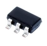
| 供应商器件封装 | SOT-23-5 |
| 偏转电压—最大值 | 3.6 mV |
| 元件数 | 1 |
| 其它名称 | 296-26822-1 |
| 制造商产品页 | http://www.ti.com/general/docs/suppproductinfo.tsp?distId=10&orderablePartNumber=TLV3401IDBVT |
| 包装 | 剪切带 (CT) |
| 单位重量 | 13 mg |
| 响应时间 | 80 us |
| 商标 | Texas Instruments |
| 安装类型 | 表面贴装 |
| 安装风格 | SMD/SMT |
| 封装 | Reel |
| 封装/外壳 | SC-74A,SOT-753 |
| 封装/箱体 | SOT-23-5 |
| 工作温度 | -40°C ~ 125°C |
| 工厂包装数量 | 250 |
| 最大功率耗散 | 385 mW |
| 最大工作温度 | + 125 C |
| 最小工作温度 | - 40 C |
| 标准包装 | 1 |
| 滞后 | - |
| 电压-电源,单/双 (±) | 2.7 V ~ 16 V, ±1.35 V ~ 8 V |
| 电压-输入失调(最大值) | 3.6mV @ 15V |
| 电压增益dB | 120 dB |
| 电流-输入偏置(最大值) | 250pA @ 15V |
| 电流-输出(典型值) | 10mA |
| 电流-静态(最大值) | 950nA |
| 电源电压-最大 | 16 V |
| 电源电压-最小 | 2.5 V |
| 电源电流—最大值 | 550 nA |
| 类型 | 通用 |
| 系列 | TLV3401 |
| 输入偏压电流—最大 | 250 pA |
| 输入类型 | Rail to Rail |
| 输出类型 | CMOS,开路漏极 |
| 通道数量 | 1 Channel |


- 商务部:美国ITC正式对集成电路等产品启动337调查
- 曝三星4nm工艺存在良率问题 高通将骁龙8 Gen1或转产台积电
- 太阳诱电将投资9.5亿元在常州建新厂生产MLCC 预计2023年完工
- 英特尔发布欧洲新工厂建设计划 深化IDM 2.0 战略
- 台积电先进制程称霸业界 有大客户加持明年业绩稳了
- 达到5530亿美元!SIA预计今年全球半导体销售额将创下新高
- 英特尔拟将自动驾驶子公司Mobileye上市 估值或超500亿美元
- 三星加码芯片和SET,合并消费电子和移动部门,撤换高东真等 CEO
- 三星电子宣布重大人事变动 还合并消费电子和移动部门
- 海关总署:前11个月进口集成电路产品价值2.52万亿元 增长14.8%


PDF Datasheet 数据手册内容提取
Product Order Technical Tools & Support & Reference Folder Now Documents Software Community Design TLV3401,TLV3402,TLV3404 SLCS135B–AUGUST2000–REVISEDJANUARY2017 TLV340x Family of Nanopower, Open-Drain Output Comparators 1 Features 3 Description • LowSupplyCurrent:470nAPerChannel The TLV340x is TI's first family of nanopower 1 comparators with only 470 nA per channel supply • InputCommon-ModeRangeExceedstheRails: current, which makes this device ideal for battery- –0.1VtoV +5V CC poweredandwirelesshandsetapplications. • SupplyVoltageRange:2.5Vto16V The TLV340x has a minimum operating supply • ReverseBatteryProtectionUpto18V voltage of 2.7 V over the extended industrial • Open-DrainCMOSOutputStage temperature range (T = –40°C to +125°C), while A having an input common-mode range of –0.1 to • SpecifiedTemperatureRange: V + 5 V. The low supply current makes it an ideal – CommercialGrade:0°Cto+70°C CC choice for battery-powered portable applications – IndustrialGrade: –40°Cto+125°C where quiescent current is the primary concern. • Ultra-SmallPackaging: Reverse battery protection guards the amplifier from an overcurrent condition due to improper battery – 5-PinSOT-23(TLV3401) installation. For harsh environments, the inputs can – 8-PinMSOP(TLV3402) be taken 5 V above the positive supply rail without • UniversalOpAmpEVM(SeeUniversal damagetothedevice. OperationalAmplifierEvaluationModuleSelection All members are available in PDIP and SOIC with the GuideForMoreInformation) single versions in the small SOT-23 package, dual versions in the VSSOP package, and quad versions 2 Applications intheTSSOPpackage. • PortableMedicalEquipment DeviceInformation(1) • WirelessSecuritySystems PARTNUMBER PACKAGE BODYSIZE(NOM) • RemoteControlSystems TLV3401 SOT-23(5) 2.90mm×1.60mm • HandheldInstruments TLV3401,TLV3402 SOIC(8) 4.90mm×3.91mm • Ultra-LowPowerSystems TLV3401,TLV3402 PDIP(8) 9.81mm×6.35mm TLV3402 VSSOP(8) 3.00mm×3.00mm SupplyCurrentvsSupplyVoltage SOIC(14) 8.65mm×3.91mm 700 T = 125°C TLV3404 TSSOP(14) 5.00mm×4.40mm A 600 PDIP(14) 19.30mm×6.35mm A) 500 TA= 70°C TA= 25°C (1) For all available packages, see the orderable addendum at n theendofthedatasheet. ent ( 400 urr T =-40°C T = 0°C High-SideVoltageSenseCircuit C A A y 300 pl p Su 200 R1 R3 R4 1 MW 100 kW 1 MW 100 0 VID=-1 V VCC + TLV340x mP R2 0 2 4 6 8 10 12 14 16 1 MW VREF Supply Voltage (V) 0 D1 0 Copyright © 2000,Texas Instruments Incorporated 1 An IMPORTANT NOTICE at the end of this data sheet addresses availability, warranty, changes, use in safety-critical applications, intellectualpropertymattersandotherimportantdisclaimers.PRODUCTIONDATA.
TLV3401,TLV3402,TLV3404 SLCS135B–AUGUST2000–REVISEDJANUARY2017 www.ti.com Table of Contents 1 Features.................................................................. 1 8.3 FeatureDescription.................................................12 2 Applications........................................................... 1 8.4 DeviceFunctionalModes........................................12 3 Description............................................................. 1 9 ApplicationandImplementation........................ 13 4 RevisionHistory..................................................... 2 9.1 ApplicationInformation............................................13 9.2 TypicalApplication .................................................13 5 DeviceComparisonTable..................................... 3 10 PowerSupplyRecommendations..................... 15 6 PinConfigurationandFunctions......................... 4 11 Layout................................................................... 15 7 Specifications......................................................... 6 11.1 LayoutGuidelines.................................................15 7.1 AbsoluteMaximumRatings......................................6 11.2 LayoutExample....................................................15 7.2 ESDRatings..............................................................6 12 DeviceandDocumentationSupport................. 16 7.3 RecommendedOperatingConditions.......................6 7.4 ThermalInformation:TLV3401.................................7 12.1 DeviceSupport......................................................16 7.5 ThermalInformation:TLV3402.................................7 12.2 DocumentationSupport........................................16 7.6 ThermalInformation:TLV3404.................................7 12.3 RelatedLinks........................................................16 7.7 ElectricalCharacteristics...........................................8 12.4 ReceivingNotificationofDocumentationUpdates16 7.8 SwitchingCharacteristics..........................................8 12.5 CommunityResource............................................17 7.9 TypicalCharacteristics..............................................9 12.6 Trademarks...........................................................17 12.7 ElectrostaticDischargeCaution............................17 8 DetailedDescription............................................ 12 12.8 Glossary................................................................17 8.1 Overview.................................................................12 13 Mechanical,Packaging,andOrderable 8.2 FunctionalBlockDiagram.......................................12 Information........................................................... 17 4 Revision History NOTE:Pagenumbersforpreviousrevisionsmaydifferfrompagenumbersinthecurrentversion. ChangesfromRevisionA(November2000)toRevisionB Page • AddedESDRatingtable,FeatureDescriptionsection,DeviceFunctionalModes,ApplicationandImplementation section,PowerSupplyRecommendationssection,Layoutsection,DeviceandDocumentationSupportsection,and Mechanical,Packaging,andOrderableInformationsection; ................................................................................................ 1 • DeletedAvailableOptionstables;refertoPackageOptionAddendumattheendofthisdatasheet................................... 3 • DeletedDissipationRatingstable........................................................................................................................................... 6 2 SubmitDocumentationFeedback Copyright©2000–2017,TexasInstrumentsIncorporated ProductFolderLinks:TLV3401 TLV3402 TLV3404
TLV3401,TLV3402,TLV3404 www.ti.com SLCS135B–AUGUST2000–REVISEDJANUARY2017 5 Device Comparison Table DEVICE(1) V (V) V (µV) ICC/Ch I (pA) t (µs) t (µs) t (µs) t (µs) RAIL-TO- OUTPUT CC IO (µA) IB PLH PHL F R RAIL STAGE TLV340x 2.5to16 250 0.47 80 55 30 5 — Input OD TLV370x 2.5to16 250 0.47 80 25 30 5 3.5 Input PP TLC3702/4 3to16 1200 9 5 1.1 0.65 0.5 0.125 — PP TLC393/339 3to16 1400 11 5 1.1 0.55 0.22 — — OD TLC372/4 3to16 1000 75 5 0.65 0.65 — — — OD (1) Allspecificationsaretypicalvaluesmeasuredat5V. Copyright©2000–2017,TexasInstrumentsIncorporated SubmitDocumentationFeedback 3 ProductFolderLinks:TLV3401 TLV3402 TLV3404
TLV3401,TLV3402,TLV3404 SLCS135B–AUGUST2000–REVISEDJANUARY2017 www.ti.com 6 Pin Configuration and Functions TLV3401:DBVPackage TLV3401:DandPPackages 5-PinSOT-23 8-PinSOICandVSSOP TopView TopView OUT 1 5 VCC NC 1 8 NC IN- 2 7 VCC GND 2 IN+ 3 6 OUT GND 4 5 NC IN+ 3 4 IN- PinFunctions:TLV3401 PIN TLV3401 I/O DESCRIPTION NAME SOT-23 SOIC,PDIP GND 2 4 — Ground IN– 4 2 I Negative(inverting)input IN+ 3 3 I Positive(noninverting)input NC — 1,5,8 — Nointernalconnection(canbeleftfloating) OUT 1 6 O Output V 5 7 — Positivepowersupply CC TLV3402:D,DGK,andPPackages 8-PINSOIC,PDIP,andVSSOP TopView 1OUT 1 8 VCC 1IN- 2 7 2OUT 1IN+ 3 6 2IN- GND 4 5 2IN+ PinFunctions:TLV3402 PIN TLV3402 I/O DESCRIPTION NAME SOIC,PDIP, VSSOP GND 4 — Ground 1IN– 2 I Invertinginput,channel1 2IN– 6 I Invertinginput,channel2 1IN+ 3 I Noninvertinginput,channel1 2IN+ 5 I Noninvertinginput,channel2 1OUT 1 O Output,channel1 2OUT 7 O Output,channel2 V 8 — Positivepowersupply CC 4 SubmitDocumentationFeedback Copyright©2000–2017,TexasInstrumentsIncorporated ProductFolderLinks:TLV3401 TLV3402 TLV3404
TLV3401,TLV3402,TLV3404 www.ti.com SLCS135B–AUGUST2000–REVISEDJANUARY2017 TLV3404:D,N,andPWPackages 14-PINSOIC,PDIP,TSSOP TopView 1OUT 1 14 4OUT 1IN- 2 13 4IN- 1IN+ 3 12 4IN+ VCC 4 11 GND 2IN+ 5 10 3IN+ 2IN- 6 9 3IN- 2OUT 7 8 3OUT PinFunctions:TLV3404 PIN TLV3404 I/O DESCRIPTION NAME SOIC,PDIP, TSSOP GND 11 — Ground 1IN– 2 I Invertinginput,channel1 2IN– 6 I Invertinginput,channel2 3IN– 9 I Invertinginput,channel3 4IN– 13 I Invertinginput,channel4 1IN+ 3 I Noninvertinginput,channel1 2IN+ 5 I Noninvertinginput,channel2 3IN+ 10 I Noninvertinginput,channel3 4IN+ 12 I Noninvertinginput,channel4 1OUT 1 O Output,channel1 2OUT 7 O Output,channel2 3OUT 8 O Output,channel3 4OUT 14 O Output,channel4 V 4 — Positivepowersupply CC Copyright©2000–2017,TexasInstrumentsIncorporated SubmitDocumentationFeedback 5 ProductFolderLinks:TLV3401 TLV3402 TLV3404
TLV3401,TLV3402,TLV3404 SLCS135B–AUGUST2000–REVISEDJANUARY2017 www.ti.com 7 Specifications 7.1 Absolute Maximum Ratings overoperatingfree-airtemperaturerange(unlessotherwisenoted)(1) MIN MAX UNIT Supply,V (2) 17 CC Voltage Differentialinput,V –20 20 V ID Input,V(2)(3) 0 V +5 I CC Input,I –10 10 I Current mA Output,I –10 10 O C-suffixversions 0 70 Operating,T A I-suffixversions –40 125 Temperature °C Junction,T 150 J Storage,T –65 150 stg (1) StressesbeyondthoselistedunderAbsoluteMaximumRatingsmaycausepermanentdamagetothedevice.Thesearestressratings only,whichdonotimplyfunctionaloperationofthedeviceattheseoranyotherconditionsbeyondthoseindicatedunderRecommended OperatingConditions.Exposuretoabsolute-maximum-ratedconditionsforextendedperiodsmayaffectdevicereliability. (2) Allvoltagevalues,exceptdifferentialvoltages,arewithrespecttoGND. (3) Inputvoltagerangeislimitedto20VorV +5V,whicheverissmaller. CC 7.2 ESD Ratings VALUE UNIT Human-bodymodel(HBM),perANSI/ESDA/JEDECJS-001(1) ±2000 V Electrostaticdischarge Charged-devicemodel(CDM),perJEDECspecificationJESD22-C101(2) ±1500 V (ESD) Machinemodel(MM) ±100 (1) JEDECdocumentJEP155statesthat500-VHBMallowssafemanufacturingwithastandardESDcontrolprocess. (2) JEDECdocumentJEP157statesthat250-VCDMallowssafemanufacturingwithastandardESDcontrolprocess. 7.3 Recommended Operating Conditions MIN MAX UNIT C-suffixversions 2.5 16 Singlesupply I-suffixversions 2.7 16 Supplyvoltage,V V CC C-suffixversions ±1.25 ±8 Splitsupply I-suffixversions ±1.35 ±8 Common-modeinputvoltage,V –0.1 V +5 V ICR CC Operatingfree-air C-suffixversions 0 70 °C temperature,TA I-suffixversions –40 125 6 SubmitDocumentationFeedback Copyright©2000–2017,TexasInstrumentsIncorporated ProductFolderLinks:TLV3401 TLV3402 TLV3404
TLV3401,TLV3402,TLV3404 www.ti.com SLCS135B–AUGUST2000–REVISEDJANUARY2017 7.4 Thermal Information: TLV3401 TLV3401 THERMALMETRIC(1) D(SOIC) DBV(SOT-23) P(PDIP) UNIT 8PINS 5PINS 8PINS R Junction-to-ambientthermalresistance 201.9 237.8 58.5 °C/W θJA R Junction-to-case(top)thermalresistance 92.5 108.7 48.3 °C/W θJC(top) R Junction-to-boardthermalresistance 123.3 64.1 35.6 °C/W θJB ψ Junction-to-topcharacterizationparameter 23 12.1 25.9 °C/W JT ψ Junction-to-boardcharacterizationparameter 212.6 63.3 35.5 °C/W JB R Junction-to-case(bottom)thermalresistance — — — °C/W θJC(bot) (1) Formoreinformationabouttraditionalandnewthermalmetrics,seetheapplicationreport,SemiconductorandICPackageThermal Metrics 7.5 Thermal Information: TLV3402 TLV3402 THERMALMETRIC(1) D(SOIC) DGK(VSSOP) P(PDIP) UNIT 8PINS 8PINS 8PINS R Junction-to-ambientthermalresistance 201.9 186.8 58.5 °C/W θJA R Junction-to-case(top)thermalresistance 92.5 77.5 48.3 °C/W θJC(top) R Junction-to-boardthermalresistance 123.3 107.8 35.6 °C/W θJB ψ Junction-to-topcharacterizationparameter 23 15.7 25.9 °C/W JT ψ Junction-to-boardcharacterizationparameter 212.6 106.2 35.5 °C/W JB R Junction-to-case(bottom)thermalresistance — — — °C/W θJC(bot) (1) Formoreinformationabouttraditionalandnewthermalmetrics,seetheapplicationreport,SemiconductorandICPackageThermal Metrics 7.6 Thermal Information: TLV3404 TLV3404 THERMALMETRIC(1) D(SOIC) N(PDIP) PW(TSSOP) UNIT 14PINS 14PINS 14PINS R Junction-to-ambientthermalresistance 83.8 65.5 120.8 °C/W θJA R Junction-to-case(top)thermalresistance 70.7 20.0 34.3 °C/W θJC(top) R Junction-to-boardthermalresistance 59.5 25.9 62.8 °C/W θJB ψ Junction-to-topcharacterizationparameter 11.6 1.9 1 °C/W JT ψ Junction-to-boardcharacterizationparameter 37.7 25.3 56.5 °C/W JB R Junction-to-case(bottom)thermalresistance — — — °C/W θJC(bot) (1) Formoreinformationabouttraditionalandnewthermalmetrics,seetheapplicationreport,SemiconductorandICPackageThermal Metrics Copyright©2000–2017,TexasInstrumentsIncorporated SubmitDocumentationFeedback 7 ProductFolderLinks:TLV3401 TLV3402 TLV3404
TLV3401,TLV3402,TLV3404 SLCS135B–AUGUST2000–REVISEDJANUARY2017 www.ti.com 7.7 Electrical Characteristics Atspecifiedfree-airtemperatureandV =2.7V,5V,15V,unlessotherwisenoted. CC PARAMETER TESTCONDITIONS T (1) MIN TYP MAX UNIT A DCPERFORMANCE T =25°C 250 3600 A V Inputoffsetvoltage V =V /2,R =50Ω,R =1MΩ µV IO IC CC S P Fullrange 4400 α Offsetvoltagedrift V =V /2,R =50Ω,R =1MΩ T =25°C 3 µV/°C VIO IC CC S P A T =25°C 55 72 A V =0Vto2.7V,R =50Ω IC S Fullrange 50 T =25°C 60 76 A CMRR Common-moderejectionratio V =0Vto5V,R =50Ω dB IC S Fullrange 55 T =25°C 65 88 A V =0Vto15V,R =50Ω IC S Fullrange 60 Large-signaldifferentialvoltage A R =1MΩ T =25°C 1000 V/mV VD amplification P A INPUT/OUTPUTCHARACTERISTICS T =25°C 20 100 A I Inputoffsetcurrent V =V /2,R =50Ω,R =1MΩ pA IO IC CC S P Fullrange 1000 T =25°C 80 250 A I Inputbiascurrent V =V /2,R =50Ω,R =1MΩ pA IB IC CC S P Fullrange 1500 r Differentialinputresistance T =25°C 300 MΩ i(d) A High-impedanceoutputleakage I V =V /2,V =V ,V =1V T =25°C 50 pA OZ current IC CC O CC ID A V =V /2,I =2µA,V =–1V T =25°C 8 IC CC OL ID A V Low-leveloutputvoltage T =25°C 80 200 mV OL A V =V /2,I =50µA,V =–1V IC CC OL ID Fullrange 300 POWERSUPPLY T =25°C 470 550 A Outputstatelow Fullrange 750 I Supplycurrent(perchannel) R =nopullup nA CC P T =25°C 560 640 A Outputstatehigh Fullrange 950 VCC=2.7Vto TA=25°C 75 100 V =V /2,no 5V Fullrange 70 PSRR Power-supplyrejectionratio IC CC dB load T =25°C 85 105 A V =5Vto15V CC Fullrange 80 (1) Fullrangeis0°Cto70°CfortheC-suffixand–40°Cto125°CfortheI-suffix.Ifnotspecified,fullrangeis–40°Cto125°C. 7.8 Switching Characteristics AtT =25°C,recommendedoperatingconditions,andV =2.7V,5V,15V,unlessotherwisenoted. A CC PARAMETER TESTCONDITIONS T MIN TYP MAX UNIT A Overdrive=2mV T =25°C 175 A Overdrive=10 Propagationdelaytime, f=10kHz,V =1V, T =25°C 80 t STEP mV A µs (PLH) low-to-high-leveloutput R =1MΩ,C =10pF P L Overdrive=50 T =25°C 55 mV A Overdrive=2mV T =25°C 300 A Overdrive=10 Propagationdelaytime, f=10kHz,V =1V, T =25°C 60 t STEP mV A µs (PHL) high-to-low-leveloutput R =1MΩ,C =10pF P L Overdrive=50 T =25°C 30 mV A t Falltime R =1MΩ,C =10pF T =25°C 5 µs F P L A 8 SubmitDocumentationFeedback Copyright©2000–2017,TexasInstrumentsIncorporated ProductFolderLinks:TLV3401 TLV3402 TLV3404
TLV3401,TLV3402,TLV3404 www.ti.com SLCS135B–AUGUST2000–REVISEDJANUARY2017 7.9 Typical Characteristics Table1.TableofGraphs DESCRIPTION FIGURENO. Inputbias/offsetcurrent vsFree-airtemperature Figure1 Opencollectorleakagecurrent vsFree-airtemperature Figure2 Figure3,Figure4, V Low-leveloutputvoltage vsLow-leveloutputcurrent OL Figure5 I Supplycurrent vsSupplyvoltage Figure6 DD I Supplycurrent vsFree-airtemperature Figure7 DD Low-to-highleveloutputresponseforvarious Figure8,Figure9, inputoverdrives Figure10 High-to-lowleveloutputresponseforvarious Figure11,Figure12, inputoverdrives Figure13 Outputfalltime vsSupplyvoltage Figure14 1200 2400 VCC= 15 V pA) 2200 VID= 1 V ent (pA) 1080000 IIB Current ( 211068000000 VCC= 15 V Input Bias/Offset Curr 6420000000 IIO en-Collector Leakage 111240846200000000000000 VCC= 2.7 V, 5 V Op 0 -200 -200 -40 -25 -10 5 20 35 50 65 80 95 110 125 -40 -25 -10 5 20 35 50 65 80 95 110 125 Temperature (°C) Temperature (°C) Figure1.InputBias/OffsetCurrentvs Figure2.Open-CollectorLeakageCurrentvs Free-AirTemperature Free-AirTemperature 2.7 5 V = 2.7 V V = 5 V 2.4 CC 4.5 CC e (V) 2.1 VID=-1 V TA= 125°C e (V) 4 VID=-1 V T = 125°C Voltag 1.8 TA= 70°C Voltag 3.53 A put 1.5 T = 25°C put 2.5 TA= 70°C Low-Level Out 001...962 A TA=-40°CTA= 0°C Low-Level Out 1.521 T =-40°CTA= 0°C TA= 25°C 0.3 0.5 A 0 0 0 0.1 0.2 0.3 0.4 0.5 0.6 0.7 0.8 0 0.4 0.8 1.2 1.6 2 2.4 2.8 Low-Level Output Current (mA) Low-Level Output Current (mA) Figure3.Low-LevelOutputVoltagevs Figure4.Low-LevelOutputVoltagevs Low-LevelOutputCurrent Low-LevelOutputCurrent Copyright©2000–2017,TexasInstrumentsIncorporated SubmitDocumentationFeedback 9 ProductFolderLinks:TLV3401 TLV3402 TLV3404
TLV3401,TLV3402,TLV3404 SLCS135B–AUGUST2000–REVISEDJANUARY2017 www.ti.com 15 700 13.5 VCC= 15 V TA= 125°C e (V) 12 VID=-1 V TA= 125°C 600 TA= 70°C TA= 25°C utput Voltag107..559 T = 25T°AC= 70°C Current (nA) 540000 TA=-40°C TA= 0°C Low-Level O 41..5536 A TA=-40°C TA= 0°C Supply 321000000 V =-1 V ID 0 0 0 1 2 3 4 5 6 7 8 9 0 2 4 6 8 10 12 14 16 Low-Level Output Current (mA) Supply Voltage (V) Figure5.Low-LevelOutputVoltagevs Figure6.SupplyCurrentvsSupplyVoltage Low-LevelOutputCurrent 700 3 V = 2.7 V, 5 V, 15 V 600 VCIDC=-1 V ge (V) 2.52 Current (nA) 540000 Output Volta 10..515 50 mV 10 mV 2 mV Supply 320000 0 RPV=C 1C M= W2.7(p Vu,l lC uLp =to 1 V0 CpCF) 0.1 al Inpute (V) 1000 TA= 25°C 00.05 DifferentiVoltag -40 -25 -10 5 20 35 50 65 80 95 110 125 -50 0 50 100 150 200 250 300 Temperature (°C) Time (ms) Figure7.SupplyCurrentvsFree-AirTemperature Figure8.Low-to-HighLevelOutputResponse forVariousInputOverdrives 5 16 utput Voltage (V) 3421 50 mV 10 mV 2 mV put Voltage (V) 11186042 10 mV 2 mV O ut 4 0 O 50 mV RP= 1 MW(pullC uTVLpAC =Ct=o 1 = 2V0 55 Cp° CCVF) 000..015 Differential InputVoltage (V) 02 RP=V C1C M=W 15(p Vu,l lC uTLpA =t=o 1 2V05 Cp°CCF) 000..015 Differential InputVoltage (V) -50 0 50 100 150 200 250 300 -50 0 50 100 150 200 250 300 Time (ms) Time (ms) Figure9.Low-to-HighLevelOutputResponse Figure10.Low-to-HighLevelOutputResponse forVariousInputOverdrives forVariousInputOverdrives 10 SubmitDocumentationFeedback Copyright©2000–2017,TexasInstrumentsIncorporated ProductFolderLinks:TLV3401 TLV3402 TLV3404
TLV3401,TLV3402,TLV3404 www.ti.com SLCS135B–AUGUST2000–REVISEDJANUARY2017 3 6 Output Voltage (V) 210...55521 50 mV 10 mV 2 mV Output Voltage (V) 530421 50 mV 10 mV 2 mV 0 RPV=C 1C M= W2.7(p Vu,l lC uTLpA =t=o 1 2V05 Cp°CCF) 000..015 Differential InputVoltage (V) -1 RP= 1 MW(pullC uTVLpAC =Ct=o 1 = 2V0 55 Cp° CCVF) 000..015 Differential InputVoltage (V) -50 0 50 100 150 200 250 300 350 400 -50 0 50 100 150 200 250 300 350 400 Time (ms) Time (ms) Figure11.High-to-LowLevelOutputResponse Figure12.High-to-LowLevelOutputResponse forVariousInputOverdrives forVariousInputOverdrives 16 8 V = 1 V to-1 V,T = 25°C 14 ID A V) 7 R = 1 mW(pull up to V ) age ( 1102 50 mV 6 InPput FallTime = 500 nsCC Volt 8 10 mV 2 mV s)m CL= 50 pF put 6 me ( 5 CL= 10 pF ut 4 Ti 4 O 02 VCC= 15 V, CL= 10 pF 0.1 al Inpute (V) Output Fall 32 RP= 1 MW(pull up to VCC),TA= 25°C 00.05 DifferentiVoltag 01 -50 0 50 100 150 200 250 300 350 400 2 3 4 5 6 7 8 9 10 11 12 13 14 15 Time (ms) Supply Voltage (V) Figure13.High-to-LowLevelOutputResponse Figure14.OutputFallTimevsSupplyVoltage forVariousInputOverdrives Copyright©2000–2017,TexasInstrumentsIncorporated SubmitDocumentationFeedback 11 ProductFolderLinks:TLV3401 TLV3402 TLV3404
TLV3401,TLV3402,TLV3404 SLCS135B–AUGUST2000–REVISEDJANUARY2017 www.ti.com 8 Detailed Description 8.1 Overview The TLV340x is a family of nanopower comparators drawing only 470 nA per channel supply current. Having a minimum operating supply voltage of 2.7 V over the extended industrial temperature range (T = –40°C to A +125°C), while having an input common-mode range of –0.1 to V + 5 V makes this device ideal for battery- CC poweredandwirelesshandsetapplications. 8.2 Functional Block Diagram VCC IN+ OUT IN– GND Copyright © 2016, Texas Instruments Incorporated 8.3 Feature Description 8.3.1 OperatingVoltage The TLV340x comparators are specified for use on a single supply from 2.5 V to 16 V (or a dual supply from ±1.25Vto ±16V)overatemperaturerangeof −40°Cto+125°C. 8.3.2 SettingtheThreshold Using a low-power, stable reference is important when setting the transition point for the TLV340x devices. The REF3312, as shown in Figure 15, provides a 1.25-V reference voltage with low drift and only 3.9 µA of quiescent current. VS Pull-up voltage Input voltage IN+ VCC RPULL-UP Output voltage OUT VS REF3312 IN– GND 1.25 V threshold voltage Copyright © 2016, Texas Instruments Incorporated Figure15. SettingtheThreshold 8.4 Device Functional Modes The TLV340x has a single functional mode and is operational when the power supply voltage applied ranges from2.5V(±1.25V)to16V(±8V). 12 SubmitDocumentationFeedback Copyright©2000–2017,TexasInstrumentsIncorporated ProductFolderLinks:TLV3401 TLV3402 TLV3404
TLV3401,TLV3402,TLV3404 www.ti.com SLCS135B–AUGUST2000–REVISEDJANUARY2017 9 Application and Implementation NOTE Information in the following applications sections is not part of the TI component specification, and TI does not warrant its accuracy or completeness. TI’s customers are responsible for determining suitability of components for their purposes. Customers should validateandtesttheirdesignimplementationtoconfirmsystemfunctionality. 9.1 Application Information Manyapplicationsrequirethedetectionofasignal(voltageorcurrent)thatexceedsaparticularthresholdvoltage or current. Using a comparator to make that threshold detection is the easiest, lowest power and highest speed waytomakeathresholddetection. 9.2 Typical Application 5 V 1 M(cid:13) Input voltage IN+ VCC RPULL-UP Output voltage OUT 5 V REF3312 IN– GND 1.25 V threshold voltage Copyright © 2016, Texas Instruments Incorporated Figure16. 1.25-VThresholdDetector 9.2.1 DesignRequirements • Detectwhenasignalisaboveorbelow1.25V • Operatefromasingle5-Vpowersupply • Rail-to-railinputvoltagerangefrom0to5V • Rail-to-railoutputvoltagerangefrom0to5V 9.2.2 DetailedDesignProcedure The input voltage range in the circuit illustrated in Figure 16 is limited only by the power supply applied to the TV3401.Inthisexamplewiththeselectionofa5-V,single-supplypowersupply,theinputvoltagerangeislimited to 0 to V + 5 V, or 0 to 10 V. The threshold voltage of 1.25 V can de derived in a variety of ways. As the S TLV3401 is a very low-power device, it is desirable to also use very low power to create the threshold voltage. The REF3312 series voltage reference is selected for its stable output voltage of 1.25 V and its low power consumption of only 3.9 µA. The TLV3401 is an open-drain output comparator, requiring a pullup resistor from output to the power supply. Proper selection of the pullup resistor value requires maximizing the output voltage swing while at the same time minimizing power dissipated in the resistor when the output voltage is low. Too small of a pullup resistor can result in too much power dissipation, while too large of a pullup resistor can result in slower response times. The TLV3401 is fully specified with a 1-MΩ pullup resistor and using a 1-MΩ pullup resistorresultsinmeetingtheperformancespecificationslistedintheElectricalCharacteristics. Copyright©2000–2017,TexasInstrumentsIncorporated SubmitDocumentationFeedback 13 ProductFolderLinks:TLV3401 TLV3402 TLV3404
TLV3401,TLV3402,TLV3404 SLCS135B–AUGUST2000–REVISEDJANUARY2017 www.ti.com Typical Application (continued) 9.2.3 ApplicationCurve 6 5 V) 4 e ( g a olt 3 V ut p ut 2 O 1 0 0 1 2 3 4 5 Voltage at IN(cid:16) pin (V) Figure17. TransferFunctionfortheThresholdDetector 14 SubmitDocumentationFeedback Copyright©2000–2017,TexasInstrumentsIncorporated ProductFolderLinks:TLV3401 TLV3402 TLV3404
TLV3401,TLV3402,TLV3404 www.ti.com SLCS135B–AUGUST2000–REVISEDJANUARY2017 10 Power Supply Recommendations The TLV340x device is specified for operation from 2.5 V to 16 V (±1.25 to ±8 V); many specifications apply from –40°C to +125°C. Parameters that can exhibit significant variance with regard to operating voltage or temperaturearepresentedinTypicalCharacteristics. 11 Layout 11.1 Layout Guidelines Figure 18 shows the typical connections for the TLV340x. To minimize supply noise, power supplies must be capacitively decoupled by a 0.01-µF ceramic capacitor in parallel with a 10-µF electrolytic capacitor. Comparators are very sensitive to input noise. Proper grounding (the use of a ground plane) helps to maintain thespecifiedperformanceoftheTLV340xfamily. Forbestresults,maintainthefollowinglayoutguidelines: 1. Useaprinted-circuitboard(PCB)withagood,unbrokenlow-inductancegroundplane. 2. Placeadecouplingcapacitor(0.1-µFceramic,surface-mountcapacitor)ascloseaspossibletoV . CC 3. On the inputs and the output, keep lead lengths as short as possible to avoid unwanted parasitic feedback aroundthecomparator.Keepinputsawayfromtheoutput. 4. SolderthedevicedirectlytothePCBratherthanusingasocket. 5. For slow-moving input signals, take care to prevent parasitic feedback. A small capacitor (1000 pF or less) placedbetweentheinputscanhelpeliminateoscillationsinthetransitionregion.Thiscapacitorcausessome degradation to propagation delay when the impedance is low. The top-side ground plane runs between the outputandinputs. 6. The ground pin ground trace runs under the device up to the bypass capacitor, shielding the inputs from the outputs. 11.2 Layout Example Power supply 0.01 µF 10 (cid:29)F V+ RPULL-UP +IN OUT – IN OUT RPULL-UP Power supply 1 5 0.01 µF 10 (cid:29)F 2 + – 3 4 Not to scale +IN –IN Copyright © 2016, Texas Instruments Incorporated Figure18. TLV340xLayoutExample Copyright©2000–2017,TexasInstrumentsIncorporated SubmitDocumentationFeedback 15 ProductFolderLinks:TLV3401 TLV3402 TLV3404
TLV3401,TLV3402,TLV3404 SLCS135B–AUGUST2000–REVISEDJANUARY2017 www.ti.com 12 Device and Documentation Support 12.1 Device Support 12.1.1 DevelopmentSupport 12.1.1.1 DIPAdapterEVM The DIP Adapter EVM tool provides an easy, low-cost way to prototype small surface mount ICs. The evaluation tool these TI packages: D or U (8-pin SOIC), PW (8-pin TSSOP), DGK (8-pin MSOP), DBV (6-pin SOT-23, 5-pin SOT23, and 3-pin SOT-23), DCK (6-pin SC-70 and 5-pin SC-70), and DRL (6-pin SOT-563). The DIP Adapter EVMmayalsobeusedwithterminalstripsormaybewireddirectlytoexistingcircuits. 12.1.1.2 UniversalOpAmpEVM The Universal Op Amp EVM is a series of general-purpose, blank circuit boards that simplify prototyping circuits for a variety of IC package types. The evaluation module board design allows many different circuits to be constructed easily and quickly. Five models are offered, with each model intended for a specific package type. PDIP,SOIC,MSOP,TSSOP,andSOT-23packagesareallsupported. NOTE These boards are unpopulated, so users must provide their own ICs. TI recommends requestingseveralopampdevicesampleswhenorderingtheUniversalOpAmpEVM. 12.2 Documentation Support 12.2.1 RelatedDocumentation ThefollowingdocumentsarerelevantforusingtheTLV340xdevicesandarerecommendedforreference.Allare availablefordownloadatwww.ti.com(unlessotherwisenoted): • UniversalOpAmpEVMUserGuide (SLOU060) • HardwarePaceusingSlopeDetection(SLAU511) • BipolarHigh-voltageDifferentialInterfaceforLow-voltageComparators (TIDU039) • AC-CoupledSingleSupplyComparator (SLAU505) • ECGImplementationontheTMS320VC5505DSPMedicalDevelopmentKit (SPRAB36) • REF33xx3.9-μA,SC70-3,SOT-23-3,andUQFN-8,30-ppm/ °CDriftVoltageReference(SBOS392) 12.3 Related Links Table 2 lists quick access links. Categories include technical documents, support and community resources, toolsandsoftware,andquickaccesstosampleorbuy. Table2.RelatedLinks TECHNICAL TOOLS& SUPPORT& PARTS PRODUCTFOLDER SAMPLE&BUY DOCUMENTS SOFTWARE COMMUNITY TLV3401 Clickhere Clickhere Clickhere Clickhere Clickhere TLV3402 Clickhere Clickhere Clickhere Clickhere Clickhere TLV3404 Clickhere Clickhere Clickhere Clickhere Clickhere 12.4 Receiving Notification of Documentation Updates To receive notification of documentation updates, navigate to the device product folder on ti.com. In the upper right corner, click on Alert me to register and receive a weekly digest of any product information that has changed.Forchangedetails,reviewtherevisionhistoryincludedinanyreviseddocument. 16 SubmitDocumentationFeedback Copyright©2000–2017,TexasInstrumentsIncorporated ProductFolderLinks:TLV3401 TLV3402 TLV3404
TLV3401,TLV3402,TLV3404 www.ti.com SLCS135B–AUGUST2000–REVISEDJANUARY2017 12.5 Community Resource The following links connect to TI community resources. Linked contents are provided "AS IS" by the respective contributors. They do not constitute TI specifications and do not necessarily reflect TI's views; see TI's Terms of Use. TIE2E™OnlineCommunity TI'sEngineer-to-Engineer(E2E)Community.Createdtofostercollaboration amongengineers.Ate2e.ti.com,youcanaskquestions,shareknowledge,exploreideasandhelp solveproblemswithfellowengineers. DesignSupport TI'sDesignSupport QuicklyfindhelpfulE2Eforumsalongwithdesignsupporttoolsand contactinformationfortechnicalsupport. 12.6 Trademarks E2EisatrademarkofTexasInstruments. Allothertrademarksarethepropertyoftheirrespectiveowners. 12.7 Electrostatic Discharge Caution Thesedeviceshavelimitedbuilt-inESDprotection.Theleadsshouldbeshortedtogetherorthedeviceplacedinconductivefoam duringstorageorhandlingtopreventelectrostaticdamagetotheMOSgates. 12.8 Glossary SLYZ022—TIGlossary. Thisglossarylistsandexplainsterms,acronyms,anddefinitions. 13 Mechanical, Packaging, and Orderable Information The following pages include mechanical, packaging, and orderable information. This information is the most current data available for the designated devices. This data is subject to change without notice and revision of thisdocument.Forbrowser-basedversionsofthisdatasheet,refertotheleft-handnavigation. Copyright©2000–2017,TexasInstrumentsIncorporated SubmitDocumentationFeedback 17 ProductFolderLinks:TLV3401 TLV3402 TLV3404
PACKAGE OPTION ADDENDUM www.ti.com 6-Feb-2020 PACKAGING INFORMATION Orderable Device Status Package Type Package Pins Package Eco Plan Lead/Ball Finish MSL Peak Temp Op Temp (°C) Device Marking Samples (1) Drawing Qty (2) (6) (3) (4/5) TLV3401CD ACTIVE SOIC D 8 75 Green (RoHS NIPDAU Level-1-260C-UNLIM 0 to 70 3401C & no Sb/Br) TLV3401CDBVR ACTIVE SOT-23 DBV 5 3000 Green (RoHS NIPDAU Level-1-260C-UNLIM 0 to 70 VBDC & no Sb/Br) TLV3401CDBVT ACTIVE SOT-23 DBV 5 250 Green (RoHS NIPDAU Level-1-260C-UNLIM 0 to 70 VBDC & no Sb/Br) TLV3401ID ACTIVE SOIC D 8 75 Green (RoHS NIPDAU Level-1-260C-UNLIM -40 to 125 3401I & no Sb/Br) TLV3401IDBVR ACTIVE SOT-23 DBV 5 3000 Green (RoHS NIPDAU Level-1-260C-UNLIM -40 to 125 VBDI & no Sb/Br) TLV3401IDBVRG4 ACTIVE SOT-23 DBV 5 3000 Green (RoHS NIPDAU Level-1-260C-UNLIM -40 to 125 VBDI & no Sb/Br) TLV3401IDBVT ACTIVE SOT-23 DBV 5 250 Green (RoHS NIPDAU Level-1-260C-UNLIM -40 to 125 VBDI & no Sb/Br) TLV3401IDBVTG4 ACTIVE SOT-23 DBV 5 250 Green (RoHS NIPDAU Level-1-260C-UNLIM -40 to 125 VBDI & no Sb/Br) TLV3401IDR ACTIVE SOIC D 8 2500 Green (RoHS NIPDAU Level-1-260C-UNLIM -40 to 125 3401I & no Sb/Br) TLV3401IP ACTIVE PDIP P 8 50 Green (RoHS NIPDAU N / A for Pkg Type -40 to 125 TLV3401I & no Sb/Br) TLV3402CD ACTIVE SOIC D 8 75 Green (RoHS NIPDAU Level-1-260C-UNLIM 0 to 70 3402C & no Sb/Br) TLV3402CDG4 ACTIVE SOIC D 8 75 Green (RoHS NIPDAU Level-1-260C-UNLIM 0 to 70 3402C & no Sb/Br) TLV3402CDGK ACTIVE VSSOP DGK 8 80 Green (RoHS NIPDAU | NIPDAUAG Level-1-260C-UNLIM 0 to 70 AJJ & no Sb/Br) TLV3402CDGKR ACTIVE VSSOP DGK 8 2500 Green (RoHS NIPDAU | NIPDAUAG Level-1-260C-UNLIM 0 to 70 AJJ & no Sb/Br) TLV3402CDGKRG4 ACTIVE VSSOP DGK 8 2500 Green (RoHS NIPDAUAG Level-1-260C-UNLIM 0 to 70 AJJ & no Sb/Br) TLV3402CDR ACTIVE SOIC D 8 2500 Green (RoHS NIPDAU Level-1-260C-UNLIM 0 to 70 3402C & no Sb/Br) TLV3402CDRG4 ACTIVE SOIC D 8 2500 Green (RoHS NIPDAU Level-1-260C-UNLIM 0 to 70 3402C & no Sb/Br) Addendum-Page 1
PACKAGE OPTION ADDENDUM www.ti.com 6-Feb-2020 Orderable Device Status Package Type Package Pins Package Eco Plan Lead/Ball Finish MSL Peak Temp Op Temp (°C) Device Marking Samples (1) Drawing Qty (2) (6) (3) (4/5) TLV3402ID ACTIVE SOIC D 8 75 Green (RoHS NIPDAU Level-1-260C-UNLIM -40 to 125 3402I & no Sb/Br) TLV3402IDG4 ACTIVE SOIC D 8 75 Green (RoHS NIPDAU Level-1-260C-UNLIM -40 to 125 3402I & no Sb/Br) TLV3402IDGK ACTIVE VSSOP DGK 8 80 Green (RoHS NIPDAU | NIPDAUAG Level-1-260C-UNLIM -40 to 125 AJK & no Sb/Br) TLV3402IDGKG4 ACTIVE VSSOP DGK 8 80 Green (RoHS NIPDAUAG Level-1-260C-UNLIM -40 to 125 AJK & no Sb/Br) TLV3402IDGKR ACTIVE VSSOP DGK 8 2500 Green (RoHS NIPDAU | NIPDAUAG Level-1-260C-UNLIM -40 to 125 AJK & no Sb/Br) TLV3402IDR ACTIVE SOIC D 8 2500 Green (RoHS NIPDAU Level-1-260C-UNLIM -40 to 125 3402I & no Sb/Br) TLV3402IDRG4 ACTIVE SOIC D 8 2500 Green (RoHS NIPDAU Level-1-260C-UNLIM -40 to 125 3402I & no Sb/Br) TLV3402IP ACTIVE PDIP P 8 50 Green (RoHS NIPDAU N / A for Pkg Type -40 to 125 TLV3402I & no Sb/Br) TLV3404CD ACTIVE SOIC D 14 50 Green (RoHS NIPDAU Level-1-260C-UNLIM 0 to 70 3404C & no Sb/Br) TLV3404CDR ACTIVE SOIC D 14 2500 Green (RoHS NIPDAU Level-1-260C-UNLIM 0 to 70 3404C & no Sb/Br) TLV3404CPW ACTIVE TSSOP PW 14 90 Green (RoHS NIPDAU Level-1-260C-UNLIM 0 to 70 3404C & no Sb/Br) TLV3404CPWR ACTIVE TSSOP PW 14 2000 Green (RoHS NIPDAU Level-1-260C-UNLIM 0 to 70 3404C & no Sb/Br) TLV3404ID ACTIVE SOIC D 14 50 Green (RoHS NIPDAU Level-1-260C-UNLIM -40 to 125 3404I & no Sb/Br) TLV3404IDG4 ACTIVE SOIC D 14 50 Green (RoHS NIPDAU Level-1-260C-UNLIM -40 to 125 3404I & no Sb/Br) TLV3404IDR ACTIVE SOIC D 14 2500 Green (RoHS NIPDAU Level-1-260C-UNLIM -40 to 125 3404I & no Sb/Br) TLV3404IN ACTIVE PDIP N 14 25 Green (RoHS NIPDAU N / A for Pkg Type -40 to 125 TLV3404I & no Sb/Br) TLV3404IPW ACTIVE TSSOP PW 14 90 Green (RoHS NIPDAU Level-1-260C-UNLIM -40 to 125 3404I & no Sb/Br) TLV3404IPWR ACTIVE TSSOP PW 14 2000 Green (RoHS NIPDAU Level-1-260C-UNLIM -40 to 125 3404I & no Sb/Br) Addendum-Page 2
PACKAGE OPTION ADDENDUM www.ti.com 6-Feb-2020 Orderable Device Status Package Type Package Pins Package Eco Plan Lead/Ball Finish MSL Peak Temp Op Temp (°C) Device Marking Samples (1) Drawing Qty (2) (6) (3) (4/5) TLV3404IPWRG4 ACTIVE TSSOP PW 14 2000 Green (RoHS NIPDAU Level-1-260C-UNLIM -40 to 125 3404I & no Sb/Br) (1) The marketing status values are defined as follows: ACTIVE: Product device recommended for new designs. LIFEBUY: TI has announced that the device will be discontinued, and a lifetime-buy period is in effect. NRND: Not recommended for new designs. Device is in production to support existing customers, but TI does not recommend using this part in a new design. PREVIEW: Device has been announced but is not in production. Samples may or may not be available. OBSOLETE: TI has discontinued the production of the device. (2) RoHS: TI defines "RoHS" to mean semiconductor products that are compliant with the current EU RoHS requirements for all 10 RoHS substances, including the requirement that RoHS substance do not exceed 0.1% by weight in homogeneous materials. Where designed to be soldered at high temperatures, "RoHS" products are suitable for use in specified lead-free processes. TI may reference these types of products as "Pb-Free". RoHS Exempt: TI defines "RoHS Exempt" to mean products that contain lead but are compliant with EU RoHS pursuant to a specific EU RoHS exemption. Green: TI defines "Green" to mean the content of Chlorine (Cl) and Bromine (Br) based flame retardants meet JS709B low halogen requirements of <=1000ppm threshold. Antimony trioxide based flame retardants must also meet the <=1000ppm threshold requirement. (3) MSL, Peak Temp. - The Moisture Sensitivity Level rating according to the JEDEC industry standard classifications, and peak solder temperature. (4) There may be additional marking, which relates to the logo, the lot trace code information, or the environmental category on the device. (5) Multiple Device Markings will be inside parentheses. Only one Device Marking contained in parentheses and separated by a "~" will appear on a device. If a line is indented then it is a continuation of the previous line and the two combined represent the entire Device Marking for that device. (6) Lead/Ball Finish - Orderable Devices may have multiple material finish options. Finish options are separated by a vertical ruled line. Lead/Ball Finish values may wrap to two lines if the finish value exceeds the maximum column width. Important Information and Disclaimer:The information provided on this page represents TI's knowledge and belief as of the date that it is provided. TI bases its knowledge and belief on information provided by third parties, and makes no representation or warranty as to the accuracy of such information. Efforts are underway to better integrate information from third parties. TI has taken and continues to take reasonable steps to provide representative and accurate information but may not have conducted destructive testing or chemical analysis on incoming materials and chemicals. TI and TI suppliers consider certain information to be proprietary, and thus CAS numbers and other limited information may not be available for release. In no event shall TI's liability arising out of such information exceed the total purchase price of the TI part(s) at issue in this document sold by TI to Customer on an annual basis. Addendum-Page 3
PACKAGE MATERIALS INFORMATION www.ti.com 1-Feb-2020 TAPE AND REEL INFORMATION *Alldimensionsarenominal Device Package Package Pins SPQ Reel Reel A0 B0 K0 P1 W Pin1 Type Drawing Diameter Width (mm) (mm) (mm) (mm) (mm) Quadrant (mm) W1(mm) TLV3401CDBVR SOT-23 DBV 5 3000 180.0 8.4 3.2 3.2 1.4 4.0 8.0 Q3 TLV3401CDBVR SOT-23 DBV 5 3000 180.0 9.0 3.15 3.2 1.4 4.0 8.0 Q3 TLV3401CDBVT SOT-23 DBV 5 250 180.0 9.0 3.15 3.2 1.4 4.0 8.0 Q3 TLV3401CDBVT SOT-23 DBV 5 250 180.0 8.4 3.2 3.2 1.4 4.0 8.0 Q3 TLV3401IDBVR SOT-23 DBV 5 3000 180.0 8.4 3.2 3.2 1.4 4.0 8.0 Q3 TLV3401IDBVR SOT-23 DBV 5 3000 180.0 9.0 3.15 3.2 1.4 4.0 8.0 Q3 TLV3401IDBVT SOT-23 DBV 5 250 180.0 9.0 3.15 3.2 1.4 4.0 8.0 Q3 TLV3401IDBVT SOT-23 DBV 5 250 180.0 8.4 3.2 3.2 1.4 4.0 8.0 Q3 TLV3401IDR SOIC D 8 2500 330.0 12.4 6.4 5.2 2.1 8.0 12.0 Q1 TLV3402CDGKR VSSOP DGK 8 2500 330.0 12.4 5.3 3.4 1.4 8.0 12.0 Q1 TLV3402CDR SOIC D 8 2500 330.0 12.4 6.4 5.2 2.1 8.0 12.0 Q1 TLV3402IDGKR VSSOP DGK 8 2500 330.0 12.4 5.3 3.4 1.4 8.0 12.0 Q1 TLV3402IDR SOIC D 8 2500 330.0 12.4 6.4 5.2 2.1 8.0 12.0 Q1 TLV3404CDR SOIC D 14 2500 330.0 16.4 6.5 9.0 2.1 8.0 16.0 Q1 TLV3404CPWR TSSOP PW 14 2000 330.0 12.4 6.9 5.6 1.6 8.0 12.0 Q1 TLV3404IDR SOIC D 14 2500 330.0 16.4 6.5 9.0 2.1 8.0 16.0 Q1 TLV3404IPWR TSSOP PW 14 2000 330.0 12.4 6.9 5.6 1.6 8.0 12.0 Q1 PackMaterials-Page1
PACKAGE MATERIALS INFORMATION www.ti.com 1-Feb-2020 *Alldimensionsarenominal Device PackageType PackageDrawing Pins SPQ Length(mm) Width(mm) Height(mm) TLV3401CDBVR SOT-23 DBV 5 3000 210.0 185.0 35.0 TLV3401CDBVR SOT-23 DBV 5 3000 182.0 182.0 20.0 TLV3401CDBVT SOT-23 DBV 5 250 182.0 182.0 20.0 TLV3401CDBVT SOT-23 DBV 5 250 210.0 185.0 35.0 TLV3401IDBVR SOT-23 DBV 5 3000 210.0 185.0 35.0 TLV3401IDBVR SOT-23 DBV 5 3000 182.0 182.0 20.0 TLV3401IDBVT SOT-23 DBV 5 250 182.0 182.0 20.0 TLV3401IDBVT SOT-23 DBV 5 250 210.0 185.0 35.0 TLV3401IDR SOIC D 8 2500 340.5 338.1 20.6 TLV3402CDGKR VSSOP DGK 8 2500 364.0 364.0 27.0 TLV3402CDR SOIC D 8 2500 340.5 338.1 20.6 TLV3402IDGKR VSSOP DGK 8 2500 364.0 364.0 27.0 TLV3402IDR SOIC D 8 2500 533.4 186.0 36.0 TLV3404CDR SOIC D 14 2500 333.2 345.9 28.6 TLV3404CPWR TSSOP PW 14 2000 367.0 367.0 35.0 TLV3404IDR SOIC D 14 2500 333.2 345.9 28.6 TLV3404IPWR TSSOP PW 14 2000 367.0 367.0 35.0 PackMaterials-Page2
PACKAGE OUTLINE DBV0005A SOT-23 - 1.45 mm max height SCALE 4.000 SMALL OUTLINE TRANSISTOR C 3.0 2.6 0.1 C 1.75 1.45 1.45 B A 0.90 PIN 1 INDEX AREA 1 5 2X 0.95 3.05 2.75 1.9 1.9 2 4 3 0.5 5X 0.3 0.15 0.2 C A B (1.1) TYP 0.00 0.25 GAGE PLANE 0.22 TYP 0.08 8 TYP 0.6 0 0.3 TYP SEATING PLANE 4214839/E 09/2019 NOTES: 1. All linear dimensions are in millimeters. Any dimensions in parenthesis are for reference only. Dimensioning and tolerancing per ASME Y14.5M. 2. This drawing is subject to change without notice. 3. Refernce JEDEC MO-178. 4. Body dimensions do not include mold flash, protrusions, or gate burrs. Mold flash, protrusions, or gate burrs shall not exceed 0.15 mm per side. www.ti.com
EXAMPLE BOARD LAYOUT DBV0005A SOT-23 - 1.45 mm max height SMALL OUTLINE TRANSISTOR PKG 5X (1.1) 1 5 5X (0.6) SYMM (1.9) 2 2X (0.95) 3 4 (R0.05) TYP (2.6) LAND PATTERN EXAMPLE EXPOSED METAL SHOWN SCALE:15X SOLDER MASK SOLDER MASK METAL UNDER METAL OPENING OPENING SOLDER MASK EXPOSED METAL EXPOSED METAL 0.07 MAX 0.07 MIN ARROUND ARROUND NON SOLDER MASK SOLDER MASK DEFINED DEFINED (PREFERRED) SOLDER MASK DETAILS 4214839/E 09/2019 NOTES: (continued) 5. Publication IPC-7351 may have alternate designs. 6. Solder mask tolerances between and around signal pads can vary based on board fabrication site. www.ti.com
EXAMPLE STENCIL DESIGN DBV0005A SOT-23 - 1.45 mm max height SMALL OUTLINE TRANSISTOR PKG 5X (1.1) 1 5 5X (0.6) SYMM 2 (1.9) 2X(0.95) 3 4 (R0.05) TYP (2.6) SOLDER PASTE EXAMPLE BASED ON 0.125 mm THICK STENCIL SCALE:15X 4214839/E 09/2019 NOTES: (continued) 7. Laser cutting apertures with trapezoidal walls and rounded corners may offer better paste release. IPC-7525 may have alternate design recommendations. 8. Board assembly site may have different recommendations for stencil design. www.ti.com
None
None
None
None
PACKAGE OUTLINE D0008A SOIC - 1.75 mm max height SCALE 2.800 SMALL OUTLINE INTEGRATED CIRCUIT C SEATING PLANE .228-.244 TYP [5.80-6.19] .004 [0.1] C A PIN 1 ID AREA 6X .050 [1.27] 8 1 2X .189-.197 [4.81-5.00] .150 NOTE 3 [3.81] 4X (0 -15 ) 4 5 8X .012-.020 B .150-.157 [0.31-0.51] .069 MAX [3.81-3.98] .010 [0.25] C A B [1.75] NOTE 4 .005-.010 TYP [0.13-0.25] 4X (0 -15 ) SEE DETAIL A .010 [0.25] .004-.010 0 - 8 [0.11-0.25] .016-.050 [0.41-1.27] DETAIL A (.041) TYPICAL [1.04] 4214825/C 02/2019 NOTES: 1. Linear dimensions are in inches [millimeters]. Dimensions in parenthesis are for reference only. Controlling dimensions are in inches. Dimensioning and tolerancing per ASME Y14.5M. 2. This drawing is subject to change without notice. 3. This dimension does not include mold flash, protrusions, or gate burrs. Mold flash, protrusions, or gate burrs shall not exceed .006 [0.15] per side. 4. This dimension does not include interlead flash. 5. Reference JEDEC registration MS-012, variation AA. www.ti.com
EXAMPLE BOARD LAYOUT D0008A SOIC - 1.75 mm max height SMALL OUTLINE INTEGRATED CIRCUIT 8X (.061 ) [1.55] SYMM SEE DETAILS 1 8 8X (.024) [0.6] SYMM (R.002 ) TYP [0.05] 5 4 6X (.050 ) [1.27] (.213) [5.4] LAND PATTERN EXAMPLE EXPOSED METAL SHOWN SCALE:8X SOLDER MASK SOLDER MASK METAL OPENING OPENING METAL UNDER SOLDER MASK EXPOSED METAL EXPOSED METAL .0028 MAX .0028 MIN [0.07] [0.07] ALL AROUND ALL AROUND NON SOLDER MASK SOLDER MASK DEFINED DEFINED SOLDER MASK DETAILS 4214825/C 02/2019 NOTES: (continued) 6. Publication IPC-7351 may have alternate designs. 7. Solder mask tolerances between and around signal pads can vary based on board fabrication site. www.ti.com
EXAMPLE STENCIL DESIGN D0008A SOIC - 1.75 mm max height SMALL OUTLINE INTEGRATED CIRCUIT 8X (.061 ) [1.55] SYMM 1 8 8X (.024) [0.6] SYMM (R.002 ) TYP [0.05] 5 4 6X (.050 ) [1.27] (.213) [5.4] SOLDER PASTE EXAMPLE BASED ON .005 INCH [0.125 MM] THICK STENCIL SCALE:8X 4214825/C 02/2019 NOTES: (continued) 8. Laser cutting apertures with trapezoidal walls and rounded corners may offer better paste release. IPC-7525 may have alternate design recommendations. 9. Board assembly site may have different recommendations for stencil design. www.ti.com
None
None
None
None
IMPORTANTNOTICEANDDISCLAIMER TI PROVIDES TECHNICAL AND RELIABILITY DATA (INCLUDING DATASHEETS), DESIGN RESOURCES (INCLUDING REFERENCE DESIGNS), APPLICATION OR OTHER DESIGN ADVICE, WEB TOOLS, SAFETY INFORMATION, AND OTHER RESOURCES “AS IS” AND WITH ALL FAULTS, AND DISCLAIMS ALL WARRANTIES, EXPRESS AND IMPLIED, INCLUDING WITHOUT LIMITATION ANY IMPLIED WARRANTIES OF MERCHANTABILITY, FITNESS FOR A PARTICULAR PURPOSE OR NON-INFRINGEMENT OF THIRD PARTY INTELLECTUAL PROPERTY RIGHTS. These resources are intended for skilled developers designing with TI products. You are solely responsible for (1) selecting the appropriate TI products for your application, (2) designing, validating and testing your application, and (3) ensuring your application meets applicable standards, and any other safety, security, or other requirements. These resources are subject to change without notice. TI grants you permission to use these resources only for development of an application that uses the TI products described in the resource. Other reproduction and display of these resources is prohibited. No license is granted to any other TI intellectual property right or to any third party intellectual property right. TI disclaims responsibility for, and you will fully indemnify TI and its representatives against, any claims, damages, costs, losses, and liabilities arising out of your use of these resources. TI’s products are provided subject to TI’s Terms of Sale (www.ti.com/legal/termsofsale.html) or other applicable terms available either on ti.com or provided in conjunction with such TI products. TI’s provision of these resources does not expand or otherwise alter TI’s applicable warranties or warranty disclaimers for TI products. Mailing Address: Texas Instruments, Post Office Box 655303, Dallas, Texas 75265 Copyright © 2020, Texas Instruments Incorporated