 Datasheet下载
- 型号: TLV320AIC33IRGZR
- 制造商: Texas Instruments
- 库位|库存: xxxx|xxxx
- 要求:
| 数量阶梯 | 香港交货 | 国内含税 |
| +xxxx | $xxxx | ¥xxxx |
查看当月历史价格
查看今年历史价格
TLV320AIC33IRGZR产品简介:
ICGOO电子元器件商城为您提供TLV320AIC33IRGZR由Texas Instruments设计生产,在icgoo商城现货销售,并且可以通过原厂、代理商等渠道进行代购。 TLV320AIC33IRGZR价格参考。Texas InstrumentsTLV320AIC33IRGZR封装/规格:接口 - 编解码器, Stereo Audio Interface 24 b I²C, Serial, SPI™ 48-VQFN (7x7)。您可以下载TLV320AIC33IRGZR参考资料、Datasheet数据手册功能说明书,资料中有TLV320AIC33IRGZR 详细功能的应用电路图电压和使用方法及教程。
TLV320AIC33IRGZR是德州仪器(Texas Instruments)推出的一款高性能音频编解码器,属于接口-编解码器类别。该器件广泛应用于便携式音频设备中,适用于对音质和功耗有较高要求的场景。

典型应用场景包括:便携式媒体播放器、语音记录设备、智能终端、工业手持设备以及通信终端等。其支持立体声音频采集与回放,具备低功耗特性,适合电池供电系统。内置的可编程增益放大器(PGA)、数字麦克风接口和灵活的时钟模式,使其能够适应多种输入输出需求,如模拟麦克风、耳机和扬声器连接。

此外,该编解码器集成了10位ADC和10/25位DAC,提供良好的信噪比(SNR),确保清晰的音频质量。配合DSP或微控制器使用时,可用于实现语音处理、噪声抑制和音频增强功能,因此也常见于语音通信和语音识别系统中。

TLV320AIC33IRGZR采用小型化VQFN封装,节省PCB空间,适合紧凑型设计。通过I²C控制接口,可方便地配置工作模式和参数,提升系统集成度与开发效率。总之,该芯片在需要高集成度、低功耗和优质音频性能的嵌入式系统中具有广泛应用价值。
| 参数 | 数值 |
| ADC/DAC数 | 2 / 2 |
| ADC数量 | 2 |
| 产品目录 | 集成电路 (IC)半导体 |
| DAC数量 | 2 |
| 描述 | IC STEREO AUDIO CODEC 48-VQFN接口—CODEC Low-Pwr Stereo CODEC |
| 产品分类 | |
| 品牌 | Texas Instruments |
| 产品手册 | http://www.ti.com/litv/slas480b |
| 产品图片 |
|
| rohs | 符合RoHS无铅 / 符合限制有害物质指令(RoHS)规范要求 |
| 产品系列 | 接口 IC,接口—CODEC,Texas Instruments TLV320AIC33IRGZR- |
| 数据手册 | |
| 产品型号 | TLV320AIC33IRGZR |
| THD+噪声 | - 90 dB ADC/- 93 dB DAC |
| 三角积分 | 是 |
| 产品目录页面 | |
| 产品种类 | 接口—CODEC |
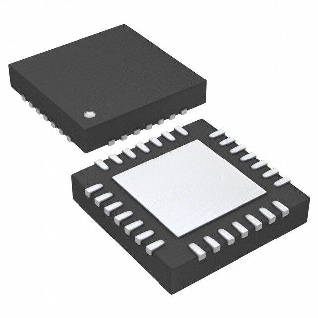
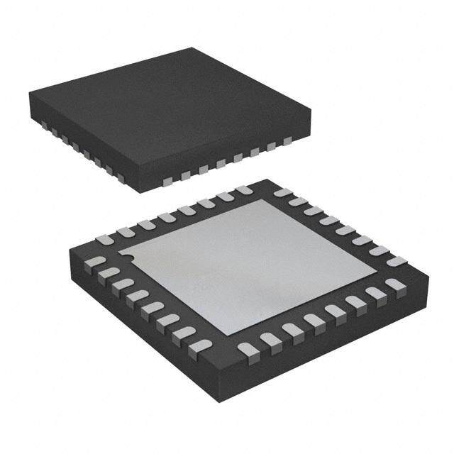
| 供应商器件封装 | 48-VQFN(7x7) |
| 信噪比 | 92 dB ADC/100 dB DAC |
| 信噪比,ADC/DAC(db)(典型值) | 92 / 100 |
| 其它名称 | 296-19789-6 |
| 分辨率 | 24 bit |
| 分辨率(位) | 24 b |
| 动态范围,ADC/DAC(db)(典型值) | 92 / 100 |
| 包装 | Digi-Reel® |
| 单位重量 | 137.400 mg |
| 商标 | Texas Instruments |
| 安装类型 | 表面贴装 |
| 安装风格 | SMD/SMT |
| 封装 | Reel |
| 封装/外壳 | 48-VFQFN 裸露焊盘 |
| 封装/箱体 | VQFN-48 |
| 工作温度 | -40°C ~ 85°C |
| 工作电源电压 | 1.1 V to 3.6 V |
| 工厂包装数量 | 2500 |
| 接口类型 | Serial (I2C, SPI) |
| 数据接口 | I²C, 串行, SPI™ |
| 最大工作温度 | + 85 C |
| 最小工作温度 | - 40 C |
| 标准包装 | 1 |
| 电压-电源,数字 | 1.65 V ~ 1.95 V |
| 电压-电源,模拟 | 2.7 V ~ 3.6 V |
| 电源电压-最大 | 3.6 V, 1.95 V |
| 电源电压-最小 | 2.7 V, 1.525 V |
| 类型 | 立体声音频 |
| 系列 | TLV320AIC33 |
| 转换速率 | 96 kHz |


- 商务部:美国ITC正式对集成电路等产品启动337调查
- 曝三星4nm工艺存在良率问题 高通将骁龙8 Gen1或转产台积电
- 太阳诱电将投资9.5亿元在常州建新厂生产MLCC 预计2023年完工
- 英特尔发布欧洲新工厂建设计划 深化IDM 2.0 战略
- 台积电先进制程称霸业界 有大客户加持明年业绩稳了
- 达到5530亿美元!SIA预计今年全球半导体销售额将创下新高
- 英特尔拟将自动驾驶子公司Mobileye上市 估值或超500亿美元
- 三星加码芯片和SET,合并消费电子和移动部门,撤换高东真等 CEO
- 三星电子宣布重大人事变动 还合并消费电子和移动部门
- 海关总署:前11个月进口集成电路产品价值2.52万亿元 增长14.8%


PDF Datasheet 数据手册内容提取
TLV320AIC33 www.ti.com........................................................................................................................................... SLAS480B–JANUARY2006–REVISEDDECEMBER2008 Low Power Stereo Audio CODEC for Portable Audio/Telephony FEATURES 7×7mm48-QFN 1 • StereoAudioDAC 23 DESCRIPTION – 100-dBASignal-to-NoiseRatio – 16/20/24/32-BitData The TLV320AIC33 is a low power stereo audio codec with stereo headphone amplifier, as well as multiple – SupportsRatesFrom8kHzto96kHz inputs and outputs programmable in single-ended or – 3D/Bass/Treble/EQ/De-emphasisEffects fully differential configurations. Extensive register- • StereoAudioADC based power control is included, enabling stereo 48-kHz DAC playback as low as 14 mW from a 3.3-V – 92-dBASignal-to-NoiseRatio analog supply, making it ideal for portable – SupportsRatesFrom8kHzto96kHz battery-poweredaudioandtelephonyapplications. • TenAudioInputPins The record path of the TLV320AIC33 contains – ProgrammableinSingle-EndedorFully integrated microphone bias, digitally controlled stereo DifferentialConfigurations microphone preamplifier, and automatic gain control – 3-StateCapabilityforFloatingInput (AGC), with mix/mux capability among the multiple analog inputs. The playback path includes mix/mux Configurations capability from the stereo DAC and selected inputs, • SevenAudioOutputDrivers through programmable volume controls, to the – Stereo8-Ω,500-mW/ChannelSpeakerDrive variousoutputs. Capability The TLV320AIC33 contains four high-power output – StereoFullyDifferentialorSingle-Ended driversaswellasthreefully differential output drivers. HeadphoneDrivers The high-power output drivers are capable of driving – FullyDifferentialStereoLineOutputs a variety of load configurations, including up to four channels of single-ended 16-Ω headphones using – FullyDifferentialMonoOutput ac-coupling capacitors, or stereo 16-Ω headphones in • LowPower:14-mWStereo48-kHzPlayback a capacitorless output configuration. In addition, pairs With3.3-VAnalogSupply ofdriverscan be used to drive 8-Ω speakers in a BTL • ProgrammableInput/OutputAnalogGains configurationat500mWperchannel. • AutomaticGainControl(AGC)forRecord The stereo audio DAC supports sampling rates from • ProgrammableMicrophoneBiasLevel 8 kHz to 96 kHz and includes programmable digital filtering in the DAC path for 3D, bass, treble, • ProgrammablePLLforFlexibleClock midrange effects, speaker equalization, and Generation de-emphasis for 32-kHz, 44.1-kHz, and 48-kHz rates. • ControlBusSelectableSPIorI2C The stereo audio ADC supports sampling rates from • AudioSerialDataBusSupportsI2S, 8 kHz to 96 kHz and is preceded by programmable gain amplifiers providing up to +59.5-dB analog gain Left/Right-Justified,DSP,andTDMModes forlow-levelmicrophoneinputs. • AlternateSerialPCM/I2SDataBusforEasy ConnectiontoBluetooth™Module The serial control bus supports SPI or I2C protocols, while the serial audio data bus is programmable for • DigitalMicrophoneInputSupport I2S, left/right-justified, DSP, or TDM modes. A highly • ExtensiveModularPowerControl programmable PLL is included for flexible clock • PowerSupplies: generation and support for all standard audio rates from a wide range of available MCLKs, varying from – Analog:2.7V–3.6V. 512 kHz to 50 MHz, with special attention paid to the – DigitalCore:1.65V–1.95V most popular cases of 12-MHz, 13-MHz, 16-MHz, – DigitalI/O:1.1V–3.6V 19.2-MHz,and19.68-MHzsystemclocks. • Packages:5×5mm80-VFBGA; 1 Pleasebeawarethatanimportantnoticeconcerningavailability,standardwarranty,anduseincriticalapplicationsofTexas Instrumentssemiconductorproductsanddisclaimerstheretoappearsattheendofthisdatasheet. MIcroStarJuniorisatrademarkofTexasInstruments. 2 BluetoothisatrademarkofBluetoothSIG,Inc.. 3 PRODUCTIONDATAinformationiscurrentasofpublicationdate. Copyright©2006–2008,TexasInstrumentsIncorporated Products conform to specifications per the terms of the Texas Instruments standard warranty. Production processing does not necessarilyincludetestingofallparameters.
TLV320AIC33 SLAS480B–JANUARY2006–REVISEDDECEMBER2008........................................................................................................................................... www.ti.com DESCRIPTION (CONTINUED) The TLV320AIC33 operates from an analog supply of 2.7 V–3.6 V, a digital core supply of 1.65 V–1.95 V, and a digital I/O supply of 1.1 V–3.6 V. The device is available in 5 × 5-mm, 80-ball MIcroStar Junior™ BGA and 7×7-mm,48-leadQFN. SIMPLIFIED BLOCK DIAGRAM HPL+ HPL−/HPLCOM HPR−/HPRCOM/SPKFC HPR+ LINE_OUT_L+ LINE_OUT_L− LINE_OUT_R+ LINE_OUT_R− MONO_OUT+ MONO−_OUT + + + + + + + M M C C V V C C AL AR D D KTKLULNCOCIWDDB Audio SerialBus Volume Ctl& Effects Volume Ctl& Effects SPI / I2C Serial ControlBus SCSMMSSRECCDESOISLLLASESOEK/EL/IGG//C/T/GGIIPP22TBPPICICOOII_OO_AADDRR10 C C DDVOI AD AD SSVD CADDDSS_DDDSSSVVVVDSRRRRVVADDDDD oltage Supplies PGA0/+59.5dB0.5dBsteps PGA0/+59.5dB0.5dBsteps Audio ClockGeneration GGMPPCIILOOK__12 CAD_DDVA V CDA_SSVA CDA_DDVA + + Bias/Reference MMIICCBDIEATS MIC2/LINE2L+MIC2/LINE2L− MIC3/LINE3L MIC1/LINE1L+MIC1/LINE1L− MIC1/LINE1R+MIC1/LINE1R− MIC3/LINE3R MIC2/LINE2R+MIC2/LINE2R− 2 SubmitDocumentationFeedback Copyright©2006–2008,TexasInstrumentsIncorporated ProductFolderLink(s):TLV320AIC33
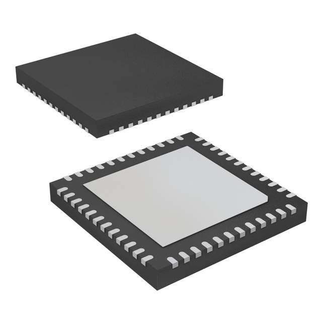
TLV320AIC33 www.ti.com........................................................................................................................................... SLAS480B–JANUARY2006–REVISEDDECEMBER2008 PACKAGING/ORDERINGINFORMATION PACKAGE OPERATING ORDERING TRANSPORT PRODUCT PACKAGE DESIGNATOR TEMPERATURE NUMBER MEDIA,QUANTITY RANGE TLV320AIC33IZQE Trays,360 ZQE TLV320AIC33IZQER TapeandReel,3000 BGA-80 TLV320AIC33IGQE Trays,360 TLV320AIC33 GQE –40°Cto85°C TLV320AIC33IGQER TapeandReel,3000 TLV320AIC33IRGZT TapeandReel,250 QFN-48 RGZ TLV320AIC33IRGZR TapeandReel,2000 PIN ASSIGNMENTS 1 1 2 4 8 1 3 J H G F E D C B 3 7 2 4 A 3 6 2 5 1 2 3 4 5 6 7 8 9 48−lead QFN Package (Bottom view) 5x5mm 80−Ball BGAPackage (Bottom View) (Not to scale) = NC ConnectQFNthermalpadtoDRVSS. TheshadedballsonBGApackagearenotconnectedtothedie,butareelectricallyconnectedtoeachother. TERMINALFUNCTIONS TERMINAL BGA DESCRIPTION QFN NAME BALL A2 13 MICBIAS MicrophoneBiasVoltageOutput A1 14 MIC3R MIC3Input(RightorMultifunction) C2,D2 15 AVSS_ADC AnalogADCGroundSupply,0V B1,C1 16,17 DRVDD ADCAnalogandOutputDriverVoltageSupply,2.7V–3.6V D1 18 HPLOUT High-PowerOutputDriver(LeftPlus) E1 19 HPLCOM High-PowerOutputDriver(LeftMinusorMultifunctional) E2,F2 20,21 DRVSS AnalogOutputDriverGroundSupply,0V F1 22 HPRCOM High-PowerOutputDriver(RightMinusorMultifunctional) G1 23 HPROUT High-PowerOutputDriver(RightPlus) H1 24 DRVDD ADCAnalogandOutputDriverVoltageSupply,2.7V–3.6V Copyright©2006–2008,TexasInstrumentsIncorporated SubmitDocumentationFeedback 3 ProductFolderLink(s):TLV320AIC33
TLV320AIC33 SLAS480B–JANUARY2006–REVISEDDECEMBER2008........................................................................................................................................... www.ti.com TERMINALFUNCTIONS(continued) TERMINAL BGA DESCRIPTION QFN NAME BALL J1 25 AVDD AnalogDACVoltageSupply,2.7V–3.6V G2,H2 26 AVSS_DAC AnalogDACGroundSupply,0V J2 27 MONO_LOP MonoLineOutput(Plus) J3 28 MONO_LOM MonoLineOutput(Minus) J4 29 LEFT_LOP LeftLineOutput(Plus) J5 30 LEFT_LOM LeftLineOutput(Minus) J6 31 RIGHT_LOP RightLineOutput(Plus) J7 32 RIGHT_LOM RightLineOutput(Minus)t H8 33 RESET Reset General-PurposeInput/Output#2(Input/Output)/DigitalMicrophoneDataInput/PLLClockInput/ J8 34 GPIO2 AudioSerialDataBusBitClockInput/Output General-PurposeInput/Output#1(Input/Output)/PLL/ClockMuxOutput/ShortCircuitInterrupt/ J9 35 GPIO1 AGCNoiseFlag/DigitalMicrophoneClockAudioSerialDataBusWordClockInput/Output H9 36 DVDD DigitalCoreVoltageSupply,1.65V–1.95V G8 37 MCLK MasterClockInputt G9 38 BCLK AudioSerialDataBusBitClock(Input/Output) F9 39 WCLK AudioSerialDataBusWordClock(Input/Output) E9 40 DIN AudioSerialDataBusDataInput(Input) F8 41 DOUT AudioSerialDataBusDataOutput(Output)t D9 42 DVSS DigitalCore/I/OGroundSupply,0V E8 43 SELECT ControlModeSelectPin(1=SPI,0=I2C) C9 44 IOVDD I/OVoltageSupply,1.1V–3.6V B8 45 MFP0 Multifunctionpin#0-SPIChipSelect/GPI/I2CAddressPin#0 B9 46 MFP1 Multifunctionpin#1-SPISerialClock/GPI/I2CAddressPin#1S A8 47 MFP2 Multifunctionpin#2-SPIMISOSlaveSerialDataOutput/GPOI A9 48 MFP3 Multifunctionpin#3-SPIMOSISlaveSerialDataInput/GPI/AudioSerialDataBusDataInput C8 1 SCL I2CSerialClock/GPIO D8 2 SDA I2CSerialDataInput/Output/GPIO A7 – NC NoConnect A6 3 LINE1LP MIC1orLine1AnalogInput(LeftPlusorMultifunction) A5 4 LINE1LM MIC1orLine1AnalogInput(LeftMinusorMultifunction) B7 5 LINE1RP MIC1orLine1AnalogInput(RightPlusorMultifunction) B6 6 LINE1RM MIC1orLine1AnalogInput(RightMinusorMultifunction) A4 7 LINE2LP MIC2orLine2AnalogInput(LeftPlusorMultifunction) B5 8 LINE2LM MIC2orLine2AnalogInput(LeftMinusorMultifunction) B4 9 LINE2RP MIC2orLine2AnalogInput(RightPlusorMultifunction) A3 10 LINE2RM MIC2orLine2AnalogInput(RightMinusorMultifunction) B3 11 MIC3L MIC3Input(LeftorMultifunction) B2 12 MICDET MicrophoneDetect C4-C7, D3-D7, E3-E7, – NC Donotconnect. F3-F7, G3-G7, H3-H7 4 SubmitDocumentationFeedback Copyright©2006–2008,TexasInstrumentsIncorporated ProductFolderLink(s):TLV320AIC33
TLV320AIC33 www.ti.com........................................................................................................................................... SLAS480B–JANUARY2006–REVISEDDECEMBER2008 ABSOLUTE MAXIMUM RATINGS overoperatingfree-airtemperaturerange(unlessotherwisenoted)(1) (2) VALUE UNIT AVDDtoAVSS,DRVDDtoDRVSS –0.3to3.9 V AVDDtoDRVSS –0.3to3.9 V IOVDDtoDVSS –0.3to3.9 V DVDDtoDVSS –0.3to2.5 V AVDDtoDRVDD –0.1to0.1 V DigitalinputvoltagetoDVSS –0.3VtoIOVDD+0.3 V AnaloginputvoltagetoAVSS –0.3VtoAVDD+0.3 V Operatingtemperaturerange -40to+85 °C Storagetemperaturerange -65to+105 °C T Max Junctiontemperature 105 °C J Powerdissipation (T Max–T )/q J A JA q Thermalimpedance,BGApackage 63 °C/W JA Thermalimpedance,QFNpackage 38.5 °C/W (1) Stressesbeyondthoselistedunderabsolutemaximumratingsmaycausepermanentdamagetothedevice.Thesearestressratings only,andfunctionaloperationofthedeviceattheseoranyotherconditionsbeyondthoseindicatedunderrecommendedoperating conditionsisnotimplied.Exposuretoabsolute-maximum-ratedconditionsforextendedperiodsmayaffectdevicereliability. (2) ESDcomplicancetestedtoEIA/JESD22-A114-Bandpassed. DISSIPATION RATINGS(1) T =25°C T =75°C T =85°C PACKAGETYPE A DERATINGFACTOR A A POWERRATING POWERRATING POWERRATING BGA 1.27W 15.9mW/°C 476mW 317mW QFN 2.08W 26.0mW/°C 779mW 519mW (1) Thisdatawastakenusing2oz.traceandcopperpadthatissoldereddirectlytoaJEDECstandard4-layer3in×3inPCB. RECOMMENDED OPERATING CONDITIONS overoperatingfree-airtemperaturerange(unlessotherwisenoted) MIN NOM MAX UNIT AVDD, Analogsupplyvoltage 2.7 3.3 3.6 V DRVDD1 /2(1) DVDD(1) Digitalcoresupplyvoltage 1.65 1.8 1.95 V IOVDD(1) DigitalI/Osupplyvoltage 1.1 1.8 3.6 V V Analogfull-scale0dBinputvoltage(DRVDD1=3.3V) 0.707 V I RMS Stereoline-outputloadresistance 10 kΩ Stereoheadphone-outputloadresistance 16 Ω Digitaloutputloadcapacitance 10 pF T Operatingfree-airtemperature –40 85 °C A (1) AnalogvoltagevaluesarewithrespecttoAVSS1,AVSS2,DRVSS;digitalvoltagevaluesarewithrespecttoDVSS. Copyright©2006–2008,TexasInstrumentsIncorporated SubmitDocumentationFeedback 5 ProductFolderLink(s):TLV320AIC33
TLV320AIC33 SLAS480B–JANUARY2006–REVISEDDECEMBER2008........................................................................................................................................... www.ti.com ELECTRICAL CHARACTERISTICS At25°C,AVDD,DRVDD,IOVDD=3.3V,DVDD=1.8V,Fs=48-kHz,16-bitaudiodata(unlessotherwisenoted) PARAMETER TESTCONDITIONS MIN TYP MAX UNIT AUDIOADC Inputsignallevel(0-dB) Single-endedinput 0.707 V RMS Signal-to-noiseratio, Fs=48kHz,0dBPGAgain,MIC1/LINE1inputs A-weighted(1) (2) selectedandAC-shortedtoground 80 92 dB Dynamicrange,A-weighted(1) (2) Fs=48kHz,1-kHz–60dBfull-scaleinputappliedat 92 dB MIC1/LINE1inputs,0-dBPGAgain Fs=48kHz,1-kHz–2dBfull-scaleinputappliedat –90 –75 dB THD Totalharmonicdistortion MIC1/LINE1inputs,0-dBPGAgain 0.003% 0.017% 234Hz,100mVpponAVDD,DRVDD,single-ended 46 Powersupplyrejectionratio input dB 234Hz,100mVpponAVDD,DRVDD,differentialinput 68 1kHz,–2dBMIC3LtoMIC3R –80 ADCchannelseparation 1kHz,–2dBMIC2LtoMIC2R –99 dB 1kHz,–2dBMIC1LtoMIC1R –-73 ADCgainerror 1kHzinput,0dBPGAgain 0.7 dB ADCprogrammablegain 1-kHzinputtone,R <50Ω 59.5 dB amplifiermaximumgain SOURCE ADCprogrammablegain 0.5 dB amplifierstepsize MIC1/LINE1inputs,routedtosingleADC 20 Inputmixattenuation=0dB MIC2/LINE2inputs,inputmixattenuation=0dB 20 MIC3/LINE3inputs,inputmixattenuation=0dB 20 Inputresistance MIC1/LINE1inputs, 80 kΩ inputmixattenuation=–12dB MIC2/LINE2inputs, 80 inputmixattenuation=–12dB MIC3/LINE3inputs, 80 inputmixattenuation=–12dB Inputcapacitance MIC1/LINE1inputs 10 pF Inputlevelcontrolminimum 0 dB attenuationsetting Inputlevelcontrolmaximum 12 dB attenuationsetting Inputlevelcontrolattenuation 1.5 dB stepsize ADCDIGITALDECIMATIONFILTER, Fs=48kHz Filtergainfrom0to0.39Fs ±0.1 dB Filtergainat0.4125Fs –0.25 dB Filtergainat0.45Fs –3 dB Filtergainat0.5Fs –17.5 dB Filtergainfrom0.55Fsto64Fs –75 dB Filtergroupdelay 17/Fs Sec (1) Ratioofoutputlevelwith1-kHzfull-scalesinewaveinput,totheoutputlevelwiththeinputsshortcircuited,measuredA-weightedovera 20-Hzto20-kHzbandwidthusinganaudioanalyzer. (2) Allperformancemeasurementsdonewith20-kHzlow-passfilterand,wherenoted,A-weightedfilter.Failuretousesuchafiltermay resultinhigherTHD+NandlowerSNRanddynamicrangereadingsthanshownintheElectricalCharacteristics.Thelow-passfilter removesout-of-bandnoise,which,althoughnotaudible,mayaffectdynamicspecificationvalues. 6 SubmitDocumentationFeedback Copyright©2006–2008,TexasInstrumentsIncorporated ProductFolderLink(s):TLV320AIC33
TLV320AIC33 www.ti.com........................................................................................................................................... SLAS480B–JANUARY2006–REVISEDDECEMBER2008 ELECTRICAL CHARACTERISTICS (continued) At25°C,AVDD,DRVDD,IOVDD=3.3V,DVDD=1.8V,Fs=48-kHz,16-bitaudiodata(unlessotherwisenoted) PARAMETER TESTCONDITIONS MIN TYP MAX UNIT MICROPHONEBIAS 2.0 2.25 2.5 2.75 Biasvoltage Programmablesettings,load=750Ω V AVDD- 0.2 Currentsourcing 2.5Vsetting 4 mA AUDIODAC DifferentialLineoutput,load=10kΩ,50pF Full-scaledifferentialoutput 0-dBgaintolineoutputs.DACoutputcommon-mode 1.414 VRMS voltage setting=1.35V,outputlevelcontrolgain=0-dB 4.0 V PP Signal-to-noiseratio, Fs=48kHz,0-dBgaintolineoutputs,zerosignal A-weighted(3) applied,referencedtofull-scaleinputlevel 90 100 dB Fs=48kHz,0-dBgaintolineoutputs, Dynamicrange,A-weighted 100 dB 1kHz–60dBsignalapplied Totalharmonicdistortion Fs=48kHz,1kHz0dBinputsignalapplied –93 –75 dB Powersupplyrejectionratio 234Hz,100mVpponAVDD,DRVDD1/2 81 dB DACchannelseparation(leftto 1-kHz,0-dB –100 dB right) DACinterchannelgainmismatch 1kHzinput,0dBgain 0.1 dB DACGainError 1kHzinput,0dBgain –0.4 dB DACDIGITALINTERPOLATION Fs=48-kHz FILTER Passband High-passfilterdisabled 0.45×Fs Hz Passbandripple High-passfilterdisabled ±0.06 dB Transitionband 0.45×Fs 0.55×Fs Hz Stopband 0.55×Fs 7.5×Fs Hz Stopbandattenuation 65 dB Groupdelay 21/Fs Sec STEREOHEADPHONEDRIVER AC-coupledoutputconfiguration(3) 0-dBgaintohighpoweroutputs.Output 0-dBfull-scaleoutputvoltage 0.707 V common-modevoltagesetting=1.35V RMS Firstoption 1.35 Programmableoutputcommon Secondoption 1.50 modevoltage(applicabletoLine V Outputsalso) Thirdoption 1.65 Fourthoption 1.8 Maximumprogrammableoutput 9 dB levelcontrolgain Programmableoutputlevel 1 dB controlgainstepsize R =32Ω 15 L P Maximumoutputpower mW O R =16Ω 30 L Signal-to-noiseratio, A-weighted(4) 94 dB (3) Unlessotherwisenoted,allmeasurementsuseoutputcommon-modevoltagesettingof1.35V,0-dBoutputlevelcontrolgain,16-Ω single-endedload. (4) Ratioofoutputlevelwitha1-kHzfull-scaleinput,totheoutputlevelplayinganall-zerosignal,measuredA-weightedovera20-Hzto 20-kHzbandwidth. Copyright©2006–2008,TexasInstrumentsIncorporated SubmitDocumentationFeedback 7 ProductFolderLink(s):TLV320AIC33
TLV320AIC33 SLAS480B–JANUARY2006–REVISEDDECEMBER2008........................................................................................................................................... www.ti.com ELECTRICAL CHARACTERISTICS (continued) At25°C,AVDD,DRVDD,IOVDD=3.3V,DVDD=1.8V,Fs=48-kHz,16-bitaudiodata(unlessotherwisenoted) PARAMETER TESTCONDITIONS MIN TYP MAX UNIT –77 1-kHzoutput,P =5mW,R =32Ω O L 0.014 –76 1-kHzoutput,P =10mW,R =32Ω O L 0.016 Totalharmonicdistortion dB% –73 1-kHzoutput,P =10mW,R =16Ω O L 0.022 –71 1-kHzoutput,P =20mW,R =16Ω O L 0.028 Channelseparation 1kHz,0dBinput 90 dB Powersupplyrejectionratio 217Hz,100mVpponAVDD,DRVDD1/2 48 dB Muteattenuation 1-kHzoutput 107 dB DIGITALI/O V Inputlowlevel I =+5-m A –0.3 0.3× V IL IL IOVDD V Inputhighlevel(5) I =+5-m A 0.7× V IH IH IOVDD 0.1× V Outputlowlevel I =2TTLloads V OL IH IOVDD 0.8× V Outputhighlevel I =2TTLloads V OH OH IOVDD SUPPLYCURRENT Fs=48-kHz AVDD+DRVDD Fs=48-kHz,PLLoff,headphone 3.0 Stereolineplayback mA DVDD driversoff,DACdirectmode 2.0 AVDD+DRVDD 2.2 Monorecord Fs=48-kHz,PLLandAGCoff mA DVDD 1.1 AVDD+DRVDD 4.2 Stereorecord Fs=48-kHz,PLLandAGCoff mA DVDD 1.3 AVDD+DRVDD Additionalpowerconsumedwhen 1.2 PLL mA DVDD PLLispowered 1 AVDD+DRVDD LINE2LP/RPonlyroutedtostereo 5.6 Headphoneamplifier single-endedheadphones,DAC mA DVDD andPLLoff,nosignalapplied 0 AVDD+DRVDD Allsupplyvoltagesapplied,all 0.1 Powerdown blocksprogrammedinlowest m A DVDD powerstate 0.5 (5) WhenIOVDD<1.6V,minimumV is1.1V. IH 8 SubmitDocumentationFeedback Copyright©2006–2008,TexasInstrumentsIncorporated ProductFolderLink(s):TLV320AIC33
TLV320AIC33 www.ti.com........................................................................................................................................... SLAS480B–JANUARY2006–REVISEDDECEMBER2008 AUDIO DATA SERIAL INTERFACE TIMING DIAGRAMS Allspecificationsat25°C,DVDD=1.8V. WCLK t (WS) d BCLK t (DO-WS) t (DO-BCLK) d d SDOUT t (DI) t (DI) S h SDIN T0145-01 IOVDD=1.1V IOVDD=3.3V PARAMETER UNIT MIN MAX MIN MAX t (WS) ADWS/WCLKdelaytime 50 15 ns d t (DO-WS) ADWS/WCLKtoDOUTdelaytime 50 20 ns d t (DO-BCLK) BCLKtoDOUTdelaytime 50 15 ns d t(DI) DINsetuptime 10 6 ns s t (DI) DINholdtime 10 6 ns h t Risetime 30 10 ns r t Falltime 30 10 ns f NOTE: Alltimingspecificationsaremeasuredatcharacterizationbutnottestedatfinaltest. Figure1.I2S/LJF/RJFTiminginMasterMode Copyright©2006–2008,TexasInstrumentsIncorporated SubmitDocumentationFeedback 9 ProductFolderLink(s):TLV320AIC33
TLV320AIC33 SLAS480B–JANUARY2006–REVISEDDECEMBER2008........................................................................................................................................... www.ti.com Allspecificationsat25°C,DVDD=1.8V. WCLK t (WS) t (WS) d d BCLK t (DO-BCLK) d SDOUT t (DI) t (DI) S h SDIN T0146-01 IOVDD=1.1V IOVDD=3.3V PARAMETER UNIT MIN MAX MIN MAX t (WS) ADWS/WCLKdelaytime 50 15 ns d t (DO-BCLK) BCLKtoDOUTdelaytime 50 15 ns d t(DI) DINsetuptime 10 6 ns s t (DI) DINholdtime 10 6 ns h t Risetime 30 10 ns r t Falltime 30 10 ns f NOTE: Alltimingspecificationsaremeasuredatcharacterizationbutnottestedatfinaltest. Figure2.DSPTiminginMasterMode 10 SubmitDocumentationFeedback Copyright©2006–2008,TexasInstrumentsIncorporated ProductFolderLink(s):TLV320AIC33
TLV320AIC33 www.ti.com........................................................................................................................................... SLAS480B–JANUARY2006–REVISEDDECEMBER2008 Allspecificationsat25°C,DVDD=1.8V. WCLK t (WS) S t (WS) h t (BCLK) H BCLK t (BCLK) t (DO-WS) L d t (DO-BCLK) d SDOUT t (DI) t (DI) S h SDIN T0145-02 IOVDD=1.1V IOVDD=3.3V PARAMETER UNIT MIN MAX MIN MAX t (BCLK) BCLKhighperiod 70 35 ns H t (BCLK) BCLKlowperiod 70 35 ns L t(WS) ADWS/WCLKsetuptime 10 6 ns s t (WS) ADWS/WCLKholdtime 10 6 ns h t (DO-WS) ADWS/WCLKtoDOUTdelaytime(forLJFModeonly) 50 35 ns d t (DO-BCLK) BCLKtoDOUTdelaytime 50 20 ns d t(DI) DINsetuptime 10 6 ns s t (DI) DINholdtime 10 6 ns h t Risetime 8 4 ns r t Falltime 8 4 ns f NOTE: Alltimingspecificationsaremeasuredatcharacterizationbutnottestedatfinaltest. Figure3.I2S/LJF/RJFTiminginSlaveMode Copyright©2006–2008,TexasInstrumentsIncorporated SubmitDocumentationFeedback 11 ProductFolderLink(s):TLV320AIC33
TLV320AIC33 SLAS480B–JANUARY2006–REVISEDDECEMBER2008........................................................................................................................................... www.ti.com Allspecificationsat25°C,DVDD=1.8V. WCLK t (WS) t (WS) S S t (WS) t (WS) h h t (BCLK) L BCLK t (BCLK) t (DO-BCLK) H d SDOUT t (DI) t (DI) S h SDIN T0146-02 IOVDD=1.1V IOVDD=3.3V PARAMETER UNIT MIN MAX MIN MAX t (BCLK) BCLKhighperiod 70 35 ns H t (BCLK) BCLKlowperiod 70 35 ns L t(WS) ADWS/WCLKsetuptime 10 8 ns s t (WS) ADWS/WCLKholdtime 10 8 ns h t (DO-BCLK) BCLKtoDOUTdelaytime 50 20 ns d t(DI) DINsetuptime 10 6 ns s t (DI) DINholdtime 10 6 ns h t Risetime 8 4 ns r t Falltime 8 4 ns f NOTE: Alltimingspecificationsaremeasuredatcharacterizationbutnottestedatfinaltest. Figure4.DSPTiminginSlaveMode 12 SubmitDocumentationFeedback Copyright©2006–2008,TexasInstrumentsIncorporated ProductFolderLink(s):TLV320AIC33
TLV320AIC33 www.ti.com........................................................................................................................................... SLAS480B–JANUARY2006–REVISEDDECEMBER2008 TYPICAL CHARACTERISTICS -20 -20 -30 B -30 d Capless, VDD = 3.6 V - n -40 AC-Coupled, o n onicDistorti --6500 AACC--CCoouupplleedd,, VVDDDD == 23..76 VV nic Distortio-4-500 VDCDap =le 2s.s7, V VVDCDDaDp =l=e 3s2.s.67, VV m o Har -70 arm -60 AC-Coupled, Total -80 Capless, VDD = 2.7 V Total H -70 VDD = 3.6 V -90 -80 0.015 0.02 0.025 0.03 0.035 0.04 Power - W -90 0.005 0.00 0.01 0.01 0.02 0.02 Power - W Figure5.HeadphonePowervsTHD,16ΩLoad Figure6.HeadphonePowervsTHD,32ΩLoad 0.00 -20.00 -40.00 -60.00 B d -80.00 -100.00 -120.00 -140.00 0 1 2 3 4 5 6 7 8 9 10 11 12 13 14 15 16 17 18 19 20 Frequency - kHz Figure7.DACtoLineOutputFFTPlot Copyright©2006–2008,TexasInstrumentsIncorporated SubmitDocumentationFeedback 13 ProductFolderLink(s):TLV320AIC33
TLV320AIC33 SLAS480B–JANUARY2006–REVISEDDECEMBER2008........................................................................................................................................... www.ti.com TYPICAL CHARACTERISTICS (continued) 0 -20 -40 -60 B d -80 -100 -120 -140 0 1 2 3 4 5 6 7 8 9 10 11 12 13 14 15 16 17 18 19 20 Frequency - kHz Figure8.LineInputtoADCFFTPlot -10.00 -20.00 -30.00 VDD = 2.7 V VDD = 3.3 V VDD = 3.6 V -40.00 D -50.00 H T -60.00 -70.00 -80.00 -90.00 0.10 0.20 0.30 0.40 0.50 0.60 Power - W Figure9.SpeakerPowervsTHD,8ΩLoad 14 SubmitDocumentationFeedback Copyright©2006–2008,TexasInstrumentsIncorporated ProductFolderLink(s):TLV320AIC33
TLV320AIC33 www.ti.com........................................................................................................................................... SLAS480B–JANUARY2006–REVISEDDECEMBER2008 TYPICAL CHARACTERISTICS (continued) 38 36 34 B d R - 32 N S 30 28 26 0 10 20 30 40 50 60 PGAGain Setting - dB Figure10.ADCSNRvsPGAGainSetting,–65dBFSInput 1.20 1.10 1.00 B d 0.90 - r o r 0.80 r E n ai 0.70 G 0.60 LeftADC RightADC 0.50 0.40 0 10 20 30 40 50 60 PGAGain Setting - dB Figure11.ADCGainErrorvsPGAGainSetting Copyright©2006–2008,TexasInstrumentsIncorporated SubmitDocumentationFeedback 15 ProductFolderLink(s):TLV320AIC33
TLV320AIC33 SLAS480B–JANUARY2006–REVISEDDECEMBER2008........................................................................................................................................... www.ti.com TYPICAL CHARACTERISTICS (continued) 3.5 3.4 3.3 3.2 MICBIAS=AVDD 3.1 3 2.9 V 2.8 - s 2.7 a bi 2.6 MICBIAS=2.5V c 2.5 Mi 2.4 2.3 2.2 MICBIAS=2.0V 2.1 2 1.9 1.8 2.7 2.8 2.9 3 3.1 3.2 3.3 3.4 3.5 3.6 AVDD - V Figure12.MICBIASOutputVoltagevsAVDD 3.2 MICBIAS=AVDD 3 2.8 V s - 2.6 MICBIAS=2.5V a bi c Mi 2.4 2.2 MICBIAS=2.0V 2 1.8 -45 -35 -25 -15 -5 5 15 25 35 45 55 65 75 85 Temp - C Figure13.MICBIASOutputVoltagevsAmbientTemperature 16 SubmitDocumentationFeedback Copyright©2006–2008,TexasInstrumentsIncorporated ProductFolderLink(s):TLV320AIC33
TLV320AIC33 www.ti.com........................................................................................................................................... SLAS480B–JANUARY2006–REVISEDDECEMBER2008 TYPICAL CHARACTERISTICS (continued) TYPICAL CIRCUIT CONFIGURATION IOVDD I2CADDRESS Multimedia DBB / Rp Processor Modem Rp RESET SCL SDA MCLK WCLK BCLK DIN DOUT MFP3 GPIO1 GPIO2 MFP2 MFP0 MFP1 AVDD (2.7V−3.6V) MICBIAS 1 kΩ 0.47mF MIC3L AAVVDDDD__DADACC mF mF mF LINE2LP DRVDD mF mF mF Handset Mic DRVDD LINE2LM mF mF mF 0.47mF 1 kΩ 0.47mF A AIC33 A (1IO.1V−D3.D3V) LINE1LP IOVDD Line In / LINE1LM 1.65−1.95V mF mF FM LINE1RP DVDD LINE1RM SELECT mF mF MONO_LOP DVSS D Analog Baseband / MONO_LOM AVSS_ADC Modem LINE2RP P M AVSS_DAC LINE2RM MICDET MIC3R HPLCOM HPRCOM HPROUTHPLOUT RIGHT_RO RIGHT_RO LEFT_LOP LEFT_LOM DDRRVVSSSS A VBAT F 560Ω 560Ω PVDD A 2 kΩ HEADSET_MIC 0.47mF Earjack mic HEADSET_GND 4700 pF and headset speakers HEADSET_SPKR_R (capless) HEADSET_SPKR_L 560Ω 560Ω 700 pF TLV320AIC33 Connections Stereo Speakers with Multiple Audio Processors PVSS TPA2012D2 Class−D SpkrAmp A Figure14.TypicalConnectionsforCaplessHeadphoneandExternalSpeakerAmp Copyright©2006–2008,TexasInstrumentsIncorporated SubmitDocumentationFeedback 17 ProductFolderLink(s):TLV320AIC33
TLV320AIC33 SLAS480B–JANUARY2006–REVISEDDECEMBER2008........................................................................................................................................... www.ti.com OVERVIEW The TLV320AIC33 is a highly flexible, low power, stereo audio codec with extensive feature integration, intended for applications in smartphones, PDAs, and portable computing, communication, and entertainment applications. Available in a 5x5mm 80-ball BGA (with 51 balls actually used) and 7x7mm 48-lead QFN, the product integrates a host of features to reduce cost, board space, and power consumption in space-constrained, battery-powered, portableapplications. TheTLV320AIC33consistsofthefollowingblocks: • Stereoaudiomulti-bitdelta-sigmaDAC(8kHz–96kHz) • Stereoaudiomulti-bitdelta-sigmaADC(8kHz–96kHz) • Programmabledigitalaudioeffectsprocessing(3-D,bass,treble,mid-range,EQ,de-emphasis) • Sixaudioinputs • Fourhigh-poweraudiooutputdrivers(headphone/speakerdrivecapability) • Threefullydifferentiallineoutputdrivers • FullyprogrammablePLL • Headphone/headsetjackdetectionwithinterrupt Communication to the TLV320AIC33 for control is pin-selectable (using the SELECT pin) as either SPI or I2C. The SPI interface requires that the Slave Select signal (MFP0) be driven low to communicate with the TLV320AIC33. Data is then shifted into or out of the TLV320AIC33 under control of the host microprocessor, which also provides the serial data clock. The I2C interface supports both standard and fast communication modes, and also enables cascading of up to four multiple codecs on the same I2C bus through the use of two pinsforaddressing(MFP0,MFP1). HARDWARE RESET The TLV320AIC33 requires a hardware reset after power-up for proper operation. After all power supplies are at their specified values, the RESET pin must be driven low for at least 10 ns. If this reset sequence is not performed,the'AIC33maynotrespondproperlytoregisterreads/writes. DIGITAL CONTROL SERIAL INTERFACE The TLV320AIC33 control interface supports SPI or I2C communication protocols, with the protocol selectable using the SELECT pin. For SPI, SELECT should be tied high; for I2C, SELECT should be tied low. It is not recommendedtochangethestateofSELECTduringdeviceoperation. SPICONTROLMODE /SS SCLK MOSI RA(6) RA(5) RA(0) D(7) D(6) D(0) 7−bit Register Address Write 8−bit Register Data MISO Figure15.SPIWrite 18 SubmitDocumentationFeedback Copyright©2006–2008,TexasInstrumentsIncorporated ProductFolderLink(s):TLV320AIC33
TLV320AIC33 www.ti.com........................................................................................................................................... SLAS480B–JANUARY2006–REVISEDDECEMBER2008 /SS SCLK MOSI RA(6) RA(5) RA(0) DON’T CARE 7-Bit Register Address Read MISO D(7) D(6) D(0) 8-Bit Register Data Figure16.SPIRead In the SPI control mode, the TLV320AIC33 uses the pins MFP0=SSB, MFP1=SCLK, MFP2=MISO, MFP3=MOSI as a standard SPI port with clock polarity setting of 0 (typical microprocessor SPI control bit CPOL = 0). The SPI port allows full-duplex, synchronous, serial communication between a host processor (the master) and peripheral devices (slaves). The SPI master (in this case, the host processor) generates the synchronizing clock (driven onto SCLK) and initiates transmissions. The SPI slave devices (such as the TLV320AIC33) depend on a master tostartandsynchronizetransmissions. A transmission begins when initiated by an SPI master. The byte from the SPI master begins shifting in on the slaveMOSIpinunderthecontrolofthemaster serial clock (driven onto SCLK). As the byte shifts in on the MOSI pin,abyteshiftsoutontheMISOpintothemastershiftregister. The TLV320AIC33 interface is designed so that with a clock phase bit setting of 1 (typical microprocessor SPI control bit CPHA = 1), the master begins driving its MOSI pin and the slave begins driving its MISO pin on the first serial clock edge. The SSB pin can remain low between transmissions; however, the TLV320AIC33 only interprets the first 8 bits transmitted after the falling edge of SSB as a command byte, and the next 8 bits as a databyteonlyifwritingtoaregister.Reservedregisterbitsshouldbewrittentotheirdefaultvalues. SPICOMMUNICATIONPROTOCOL The TLV320AIC33 is entirely controlled by registers. Reading and writing these registers is accomplished by the use of an 8-bit command, which is sent to the MOSI pin of the part prior to the data for that register. The command is constructed as shown in the Command Word table. The first 7 bits specify the register address whichisbeingwrittenorread,from0to127(decimal).Thecommandwordendswith an R/W bit, which specifies the direction of data flow on the serial bus. In the case of a register write, the R/W bit should be set to 0. A secondbyteofdataissenttotheMOSIpinandcontainsthedatatobewrittentotheregister. Reading of registers is accomplished in similar fashion. The 8-bit command word sends the 7-bit register address,followedbyR/Wbit=1tosignifyaregisterreadisoccurring,.The8-bitregister data is then clocked out ofthepartontheMISOpinduringthesecond8SCLKclocksintheframe. CommandWord Bit7 Bit6 Bit5 Bit4 Bit3 Bit2 Bit1 Bit0 ADDR6 ADDR5 ADDR4 ADDR3 ADDR2 ADDR1 ADDR0 R/W The register map of the TLV320AIC33 actually consists of multiple pages of registers, with each page containing 128 registers. The register at address zero on each page is used as a page-control register, and writing to this register determines the active page for the device. All subsequent read/write operations will access the page that is active at the time, unless a register write is performed to change the active page. Only two pages of registers areimplementedinthisproduct,withtheactivepagedefaultingtopage0upondevicereset. For example, at device reset, the active page defaults to page 0, and thus all register read/write operations for addresses 1 to 127 will access registers in page 0. If registers on page 1 must be accessed, the user must write the8-bitsequence0x01toregister0,thepagecontrolregister,tochangetheactivepagefrompage0to page 1. After this write, it is recommended the user also read back the page control register, to safely ensure the change Copyright©2006–2008,TexasInstrumentsIncorporated SubmitDocumentationFeedback 19 ProductFolderLink(s):TLV320AIC33
TLV320AIC33 SLAS480B–JANUARY2006–REVISEDDECEMBER2008........................................................................................................................................... www.ti.com in page control has occurred properly. Future read/write operations to addresses 1 to 127 will now access registers in page 1. When page 0 registers must be accessed again, the user writes the 8-bit sequence 0x00 to register 0, the page control register, to change the active page back to page 0. After a recommended read of the page control register, all further read/write operations to addresses 1 to 127 will now access page 0 registers again. LimitationonRegisterWriting When writing registers in SPI mode related to the audio output drivers mux, mix, gain configuration, etc., do not use the auto-increment mode. In addition, between two successive writes to these registers, the host should keepMFP0(SPIchipselect)highforatleast6.25us,toensurethattheregisterwriteshaveoccurredproperly. CONTINUOUSREAD/WRITEOPERATION The TLV320AIC33 includes the ability to read/write registers continuously, without needing to provide an address for every register accessed. In SPI mode, a continuous write is executed by transitioning MFP0 (SPI chip select) low to start the frame, sending the first 8-bit command word to read/write a particular register, and then sending multiple bytes of register data, intended for the addressed register and those following. A continuous read is done similarly, with multiple bytes read in from the addressed register and the following registers on the page. When the MFP0 (SPI chip select) pin is transitioned high again, the frame ends, as does the continuous read/writeoperation.Anewframemustbeginagainwithanewcommandword,tostartthenextbustransaction. Note that this continuous read/write operation does not continue past a page boundary. The user should not attempttoread/writepasttheendofapage,sincethismayresultinundesirableoperation. I2C CONTROL MODE TheTLV320AIC33supportstheI2Ccontrolprotocol when the SELECT pin is tied low, using 7-bit addressing and capable of both standard and fast modes. TLV320AIC33 supports the I2C control protocol using 7-bit addressing and capable of both standard and fast modes. For I2C fast mode, note that the minimum timing for each of tHD-STA, tSU-STA, and tSU-STO is 2.0 m s, as seen in Figure 17. When in I2C control mode, the TLV320AIC33 can be configured for one of four different addresses, using the multifunction pins MFP0 and MFP1, which controlthetwoLSBsofthedeviceaddress.The5MSBsofthedeviceaddressarefixedas00110and cannot be changed,whilethetwoLSBsaregivenbyMFP1:MFP0.Thisresultsinfourpossibledeviceaddresses: I2CslaveDeviceAddressesforMFP1,MFP0Settings MFP1 MFP0 DeviceAddress 0 0 0011000 0 1 0011001 1 0 0011010 1 1 0011011 20 SubmitDocumentationFeedback Copyright©2006–2008,TexasInstrumentsIncorporated ProductFolderLink(s):TLV320AIC33
TLV320AIC33 www.ti.com........................................................................................................................................... SLAS480B–JANUARY2006–REVISEDDECEMBER2008 SDA tHD-STA³2.0ms SCL tSU-STA³2.0ms tHD-STA³2.0ms tSU-STO³2.0ms S Sr P S T0114-02 Figure17.I2CInterfaceTiming I2C is a two-wire, open-drain interface supporting multiple devices and masters on a single bus. Devices on the I2C bus only drive the bus lines LOW by connecting them to ground; they never drive the bus lines HIGH. Instead, the bus wires are pulled HIGH by pull-up resistors, so the bus wires are HIGH when no device is driving them LOW. This way, two devices cannot conflict; if two devices drive the bus simultaneously, there is no driver contention. Communication on the I2C bus always takes place between two devices, one acting as the master and the other actingasthe slave. Both masters and slaves can read and write, but slaves can only do so under the direction of the master. Some I2C devices can act as masters or slaves, but the TLV320AIC33 can only act as a slave device. An I2C bus consists of two lines, SDA and SCL. SDA carries data; SCL provides the clock. All data is transmitted across the I2C bus in groups of eight bits. To send a bit on the I2C bus, the SDA line is driven to the appropriate level while SCL is LOW (a LOW on SDA indicates the bit is zero; a HIGH indicates the bit is one). Once the SDA line has settled, the SCL line is brought HIGH, then LOW. This pulse on SCL clocks the SDA bit into the receiversshiftregister. The I2C bus is bidirectional: the SDA line is used both for transmitting and receiving data. When a master reads from a slave, the slave drives the data line; when a master sends to a slave, the master drives the data line. Undernormalcircumstancesthemasterdrivestheclockline. Most of the time the bus is idle, no communication is taking place, and both lines are HIGH. When communicationistakingplace,thebusisactive.Onlymasterdevicescanstartacommunication. They do this by causing a START condition on the bus. Normally, the data line is only allowed to change state while the clock line is LOW. If the data line changes state while the clock line is HIGH, it is either a START condition or its counterpart, a STOP condition. A START condition is when the clock line is HIGH and the data line goes from HIGHtoLOW.ASTOPconditioniswhentheclocklineisHIGHandthedatalinegoesfromLOWtoHIGH. After the master issues a START condition, it sends a byte that indicates which slave device it wants to communicate with. This byte is called the address byte. Each device on an I2C bus has a unique 7-bit address to which it responds. (Slaves can also have 10-bit addresses; see the I2C specification for details.) The master sends an address in the address byte, together with a bit that indicates whether it wishes to read from or write to theslavedevice. Every byte transmitted on the I2C bus, whether it is address or data, is acknowledged with an acknowledge bit. When a master has finished sending a byte (eight data bits) to a slave, it stops driving SDA and waits for the slave to acknowledge the byte. The slave acknowledges the byte by pulling SDA LOW. The master then sends a clock pulse to clock the acknowledge bit. Similarly, when a master has finished reading a byte, it pulls SDA LOW toacknowledgethistotheslave.Itthensendsaclockpulsetoclockthebit. Copyright©2006–2008,TexasInstrumentsIncorporated SubmitDocumentationFeedback 21 ProductFolderLink(s):TLV320AIC33
TLV320AIC33 SLAS480B–JANUARY2006–REVISEDDECEMBER2008........................................................................................................................................... www.ti.com A not-acknowledge is performed by simply leaving SDA HIGH during an acknowledge cycle. If a device is not present on the bus, and the master attempts to address it, it will receive a not−acknowledge because no device ispresentatthataddresstopullthelineLOW. When a master has finished communicating with a slave, it may issue a STOP condition. When a STOP condition is issued, the bus becomes idle again. A master may also issue another START condition. When a STARTconditionisissuedwhilethebusisactive,itiscalledarepeatedSTARTcondition. The TLV320AIC33 also responds to and acknowledges a General Call, which consists of the master issuing a commandwithaslaveaddressbyteof00H. SCL SDA DA(6) DA(0) RA(7) RA(0) D(7) D(0) Start 7-bitDeviceAddress Write Slave 8-bitRegisterAddress Slave 8-bitRegisterData Slave Stop (M) (M) (M) Ack (M) Ack (M) Ack (M) (S) (S) (S) (M)=>SDAControlledbyMaster (S) =>SDAControlledbySlave Figure18.I2CWrite SCL SDA DA(6) DA(0) RA(7) RA(0) DA(6) DA(0) D(7) D(0) Start 7-bitDeviceAddress Write Slave 8-bitRegisterAddress Slave Repeat 7-bitDeviceAddress Read Slave 8-bitRegisterData Master Stop (M) (M) (M) Ack (M) Ack Start (M) (M) Ack (S) NoAck (M) (S) (S) (M) (S) (M) (M)=>SDAControlledbyMaster (S) =>SDAControlledbySlave Figure19.I2CRead In the case of an I2C register write, if the master does not issue a STOP condition, then the device enters auto-increment mode. So in the next eight clocks, the data on SDA is treated as data for the next incremental register. Similarly, in the case of an I2C register read, after the device has sent out the 8-bit data from the addressed register, if the master issues an ACKNOWLEDGE, the slave takes over control of SDA bus and transmit for the next8clocksthedataofthenextincrementalregister. DIGITAL AUDIO DATA SERIAL INTERFACE Audio data is transferred between the host processor and the TLV320AIC33 via the digital audio data serial interface, or audio bus. The audio bus on this device is very flexible, including left or right justified data options, support for I2S or PCM protocols, programmable data length options, a TDM mode for multichannel operation, very flexible master/slave configurability for each bus clock line, and the ability to communicate with multiple deviceswithinasystemdirectly. The data serial interface uses two sets of pins for communication between external devices, with the particular pinusedcontrolledthroughregisterprogramming.ThisconfigurationisshowninFigure20below. 22 SubmitDocumentationFeedback Copyright©2006–2008,TexasInstrumentsIncorporated ProductFolderLink(s):TLV320AIC33
TLV320AIC33 www.ti.com........................................................................................................................................... SLAS480B–JANUARY2006–REVISEDDECEMBER2008 WCLK BCLK DIN DOUT GPIO1 GPIO2 MFP3 Audio Serial Data Bus Figure20.AlternateAudioBusMulitplexingFunction In cases where MFP3 is needed for a secondary device digital input, the TLV320AIC33 must be used in I2C mode (when in SPI mode, MFP3 is used as the SPI bus MOSI pin and thus cannot be used here as an alternate digitalinputsource). This mux capability allows the TLV320AIC33 to communicate with two separate devices with independent I2S/PCM buses. An example of such an application is a cellphone containing a Bluetooth transceiver with PCM/I2S interface, as shown in Figure 21. The applications processor can be connected to the WCLK, BCLK, DIN, DOUT pins on the TLV320AIC33, while a Bluetooth device with PCM interface can be connected to the GPIO1, GPIO2, MFP3, and DOUT pins on the TLV320AIC33. By programming the registers via I2C control, the applications processor can determine which device is communicating with the TLV320AIC33. This is attractive in cases where the TLV320AIC33 can be configured to communicate data with the Bluetooth device, then the applications processor can be put into a low power sleep mode, while voice/audio transmission still occurs betweentheBluetoothdeviceandtheTLV320AIC33. Processor Processor 1 2 K K N T 3 1 2 WCL BCL DI DOU MFP GPIO GPIO AIC33 Possible ProcessorTypes: Application Processor, Multimedia Processor, CompressedAudio Decoder, Wireless Modem, Bluetooth Module,AdditionalAudio/Voice Codec Figure21.AIC33ConnectedtoMultipleAudioDevices The audio bus of the TLV320AIC33 can be configured for left or right justified, I2S, DSP, or TDM modes of operation, where communication with standard telephony PCM interfaces is supported within the TDM mode. These modes are all MSB-first, with data width programmable as 16, 20, 24, or 32 bits. In addition, the word clock (WCLK or GPIO1) and bit clock (BCLK or GPIO2) can be independently configured in either Master or Slavemode,forflexibleconnectivitytoawidevarietyofprocessors Copyright©2006–2008,TexasInstrumentsIncorporated SubmitDocumentationFeedback 23 ProductFolderLink(s):TLV320AIC33
TLV320AIC33 SLAS480B–JANUARY2006–REVISEDDECEMBER2008........................................................................................................................................... www.ti.com The word clock (WCLK or GPIO1) is used to define the beginning of a frame, and may be programmed as either a pulse or a square-wave signal. The frequency of this clock corresponds to the maximum of the selected ADC andDACsamplingfrequencies. The bit clock (BCLK or GPIO2) is used to clock in and out the digital audio data across the serial bus. When in Master mode, this signal can be programmed in two further modes: continuous transfer mode, and 256-clock mode. In continuous transfer mode, only the minimal number of bit clocks needed to transfer the audio data are generated, so in general the number of bit clocks per frame will be two times the data width. For example, if data width is chosen as 16-bits, then 32 bit clocks will be generated per frame. If the bit clock signal in master mode will be used by a PLL in another device, it is recommended that the 16-bit or 32-bit data width selections be used. These cases result in a low jitter bit clock signal being generated, having frequencies of 32×Fs or 64×Fs. In the cases of 20-bit and 24-bt data width in master mode, the bit clocks generated in each frame will not all be of equal period, due to the device not having a clean 40×Fs or 48×Fs clock signal readily available. The average frequency of the bit clock signal is still accurate in these cases (being 40×Fs or 48×Fs), but the resulting clock signalhashigherjitterthaninthe16-bitand32-bitcases. In 256-clock mode, a constant 256 bit clocks per frame are generated, independent of the data width chosen. The TLV320AIC33 further includes programmability to tri-state the DOUT line during all bit clocks when valid data is not being sent. By combining this capability with the ability to program at what bit clock in a frame the audio data will begin, time-division multiplexing (TDM) can be accomplished, resulting in multiple codecs able to useasingleaudioserialdatabus. When the audio serial data bus is powered down while configured in master mode, the pins associated with the interfacewillbeputintoatri-stateoutputcondition. RIGHT JUSTIFIED MODE In right-justified mode, the LSB of the left channel is valid on the rising edge of the bit clock preceding the falling edge of word clock. Similarly, the LSB of the right channel is valid on the rising edge of the bit clock preceding therisingedgeofthewordclock. 1/fs WCLK BCLK Left Channel Right Channel SDIN/ 0 n−1n−2 n−3 2 1 0 n−1n−2 n−3 2 1 0 SDOUT MSB LSB Figure22.RightJustifiedSerialBusModeOperation LEFT JUSTIFIED MODE In left-justified mode, the MSB of the right channel is valid on the rising edge of the bit clock following the falling edge of the word clock. Similarly the MSB of the left channel is valid on the rising edge of the bit clock following therisingedgeofthewordclock. 24 SubmitDocumentationFeedback Copyright©2006–2008,TexasInstrumentsIncorporated ProductFolderLink(s):TLV320AIC33
TLV320AIC33 www.ti.com........................................................................................................................................... SLAS480B–JANUARY2006–REVISEDDECEMBER2008 n-1 n-2 n-3 n-1 n-2 n-3 Figure23.LeftJustifiedSerialDataBusModeOperation I2S MODE In I2S mode, the MSB of the left channel is valid on the second rising edge of the bit clock after the falling edge of the word clock. Similarly the MSB of the right channel is valid on the second rising edge of the bit clock after therisingedgeofthewordclock. n-1 n-2 n-3 n-1 n-2 n-3 Figure24.I2SSerialDataBusModeOperation DSP MODE In DSP mode, the rising edge of the word clock starts the data transfer with the left channel data first and immediatelyfollowedbytherightchanneldata.Eachdatabitisvalidonthefallingedgeofthebitclock. Copyright©2006–2008,TexasInstrumentsIncorporated SubmitDocumentationFeedback 25 ProductFolderLink(s):TLV320AIC33
TLV320AIC33 SLAS480B–JANUARY2006–REVISEDDECEMBER2008........................................................................................................................................... www.ti.com 1/fs WCLK BCLK Left Channel Right Channel SDIN/SDOUT n–1 n–2 n–3 n–4 2 1 0 n–1 n–2 n–3 2 1 0 n–1 LSB MSB LSB MSB LSB T0152-01 Figure25.DSPSerialBusModeOperation TDM DATA TRANSFER Time-division multiplexed data transfer can be realized in any of the above transfer modes if the 256-clock bit clock mode is selected, although it is recommended to be used in either left-justified mode or DSP mode. By changing the programmable offset, the bit clock in each frame where the data begins can be changed, and the serial data output driver (DOUT) can also be programmed to tri-state during all bit clocks except when valid data is being put onto the bus. This allows other codecs to be programmed with different offsets and to drive their data onto the same DOUT line, just in a different slot. For incoming data, the codec simply ignores data on the busexceptwhereitisexpectedbasedontheprogrammedoffset. Note that the location of the data when an offset is programmed is different, depending on what transfer mode is selected. In DSP mode, both left and right channels of data are transferred immediately adjacent to each other in the frame. This differs from left-justified mode, where the left and right channel data will always be a half-frame apart in each frame. In this case, as the offset is programmed from zero to some higher value, both the left and right channel data move across the frame, but still stay a full half-frame apart from each other. This is depicted in Figure26forthetwocases. 26 SubmitDocumentationFeedback Copyright©2006–2008,TexasInstrumentsIncorporated ProductFolderLink(s):TLV320AIC33
TLV320AIC33 www.ti.com........................................................................................................................................... SLAS480B–JANUARY2006–REVISEDDECEMBER2008 DSPMode word clock bitclock data in/out N-1 N-2 1 0 N-1 N-2 1 0 offset Left Channel Data Right Channel Data Left Justified Mode word clock bitclock data in/out N-1 N-2 1 0 N-1 N-2 1 0 Left Channel Data Right Channel Data offset offset Figure26.DSPModeandLeftJustifiedModes,Showingthe EffectofaProgrammedDataWordOffset AUDIO DATA CONVERTERS The TLV320AIC33 supports the following standard audio sampling rates: 8 kHz, 11.025 kHz, 12 kHz, 16 kHz, 22.05 kHz, 24 kHz, 32 kHz, 44.1 kHz, 48 kHz, 88.2 kHz, and 96 kHz. The converters can also operate at differentsamplingratesinvariouscombinations,whicharedescribedfurtherbelow. Thedataconvertersare based on the concept of an Fsref rate that is used internal to the part, and it is related to the actual sampling rates of the converters through a series of ratios. For typical sampling rates, Fsref will be either 44.1 kHz or 48 kHz, although it can realistically be set over a wider range of rates up to 53 kHz, with additional restrictions applying if the PLL is used. This concept is used to set the sampling rates of the ADC and DAC, and also to enable high quality playback of low sampling rate data, without high frequency audible noise beinggenerated. The sampling rate of the ADC and DAC can be set to Fsref/NDAC or 2×Fsref/NDAC, with NDAC being 1, 1.5, 2, 2.5,3,3.5,4,4.5,5,5.5,or6. While only one Fsref can be used at a time in the part, the ADC and DAC sampling rates can differ from each other by using different NADC and NDAC divider ratios for each. For example, with Fsref=44.1-kHz, the DAC samplingratecanbesetto44.1-kHzbyusingNDAC=1,whiletheADCsampling rate can be set to 8.018-kHz by usingNADC=5.5. When the ADCs and DACs are operating at different sampling rates, an additional word clock is required, to provideinformationregardingwheredata begins for the ADC versus the DAC. In this case, the standard bit clock signal (which can be supplied through the BCLK pin or through GPIO2) is used to transfer both ADC and DAC data,thestandardwordclocksignalisusedtoidentifythestartofthe DAC data, and a separate ADC word clock signal (denoted ADWK) is used. This clock can be supplied or generated from GPIO1 at the same time the DAC wordclockissuppliedorgeneratedfromWCLK. AUDIO CLOCK GENERATION The audio converters in the TLV320AIC33 need an internal audio master clock at a frequency of 256×Fsref, whichcanbeobtainedinavarietyofmannersfromanexternalclocksignalappliedtothedevice. AmoredetaileddiagramoftheaudioclocksectionoftheTLV320AIC33isshowninFigure27. Copyright©2006–2008,TexasInstrumentsIncorporated SubmitDocumentationFeedback 27 ProductFolderLink(s):TLV320AIC33
TLV320AIC33 SLAS480B–JANUARY2006–REVISEDDECEMBER2008........................................................................................................................................... www.ti.com MCLK BCLK GPIO2 CLKDIV_CLKIN PLL_CLKIN CLKDIV_IN PLL_IN K = J.D J = 1,2,3,. . . , 62,63 Q = 3,3, . . . . ,16,17 2/Q K*R/P D= 0000,0001, . . . ,9998,9999 R= 1,2,3,4, . . . ,15,16 P= 1,2, . . . . ,7,8 CLKDIV_OUT PLL_OUT 1/8 PLLDIV_OUT CLKMUX_OUT CODEC_CLKIN CLKOUT_IN CODEC_CLK=256*Fsref M =1,2,4,8 2/(N*M) CODEC N = 2,3, . . . ., 16,17 CLKOUT DAC_FS ADC_FS GPIO1 WCLK= Fsref/Ndac GPIO1= Fsref/Nadc Ndac=1,1.5,2, . . ., 5.5,6 Ndac=1,1.5,2, . . ., 5.5,6 DAC DRA => Ndac = 0.5 ADC DRA => Nadc = 0.5 Figure27.AudioClockGenerationProcessing The part can accept an MCLK input from 512 kHz to 50 MHz, which can then be passed through either a programmable divider or a PLL, to get the proper internal audio master clock needed by the part. The BCLK or GPIO2inputscanalsobeusedtogeneratetheinternalaudiomasterclock. ThisdesignalsoallowsthePLLto be used for an entirely separate purpose in a system, if the audio codec is not poweredup.TheusercansupplyaseparateclocktoGPIO2,routethisthroughthePLL,withtheresulting output clockdrivenoutGPIO1,forusebyotherdevicesinthesystem A primary concern is proper operation of the codec at various sample rates with the limited MCLK frequencies available in the system. This device includes a highly programmable PLL to accommodate such situations easily. The integrated PLL can generate audio clocks from a wide variety of possible MCLK inputs, with particular focus paidtothestandardMCLKratesalreadywidelyused. 28 SubmitDocumentationFeedback Copyright©2006–2008,TexasInstrumentsIncorporated ProductFolderLink(s):TLV320AIC33
TLV320AIC33 www.ti.com........................................................................................................................................... SLAS480B–JANUARY2006–REVISEDDECEMBER2008 WhenthePLLisdisabled, Fsref=CLKDIV_IN/(128×Q) WhereQ=2,3,…,17 CLKDIV_INcanbeMCLK,BCLK,orGPIO2,selectedbyregister102,bitsD7-D6. NOTE – when NDAC = 1.5, 2.5, 3.5, 4.5, or 5.5, odd values of Q are not allowed. In this mode, MCLK can be as highas50MHz,andFsrefshouldfallwithin39kHzto53kHz. WhenthePLLisenabled, Fsref=(PLLCLK_IN×K×R)/(2048×P),where P=1,2,3,…,8 R=1,2,…,16 K=J.D J=1,2,3,…,63 D=0000,0001,0002,0003,…,9998,9999 PLLCLK_INcanbeMCLKorBCLK,selectedbyPage0,register102,bitsD5-D4 P, R, J, and D are register programmable. J is the integer portion of K (the numbers to the left of the decimal point), while D is the fractional portion of K (the numbers to the right of the decimal point, assuming four digits of precision). Examples: IfK=8.5,thenJ=8,D=5000 IfK=7.12,thenJ=7,D=1200 IfK=14.03,thenJ=14,D=0300 IfK=6.0004,thenJ=6,D=0004 When the PLL is enabled and D = 0000, the following conditions must be satisfied to meet specified performance: 2MHz≤(PLLCLK_IN/P)≤20MHz 80MHz≤(PLLCLK_IN×K×R/P)≤110MHz 4≤J≤55 WhenthePLLisenabledandD≠0000,thefollowingconditionsmustbesatisfiedtomeetspecifiedperformance: 10MHz≤PLLCLK_IN/P≤20MHz 80MHz≤PLLCLK_IN×K×R/P≤110MHz 4≤J≤11 R=1 Example: MCLK=12MHzandFsref=44.1kHz SelectP=1,R=1,K=7.5264,whichresultsinJ=7,D=5264 Example: MCLK=12MHzandFsref=48.0kHz SelectP=1,R=1,K=8.192,whichresultsinJ=8,D=1920 Copyright©2006–2008,TexasInstrumentsIncorporated SubmitDocumentationFeedback 29 ProductFolderLink(s):TLV320AIC33
TLV320AIC33 SLAS480B–JANUARY2006–REVISEDDECEMBER2008........................................................................................................................................... www.ti.com The table below lists several example cases of typical MCLK rates and how to program the PLL to achieve Fsref=44.1kHzor48kHz. Fsref=44.1kHz MCLK(MHz) P R J D ACHIEVEDFSREF %ERROR 2.8224 1 1 32 0 44100.00 0.0000 5.6448 1 1 16 0 44100.00 0.0000 12.0 1 1 7 5264 44100.00 0.0000 13.0 1 1 6 9474 44099.71 0.0007 16.0 1 1 5 6448 44100.00 0.0000 19.2 1 1 4 7040 44100.00 0.0000 19.68 1 1 4 5893 44100.30 –0.0007 48.0 4 1 7 5264 44100.00 0.0000 Fsref=48kHz MCLK(MHz) P R J D ACHIEVEDFSREF %ERROR 2.048 1 1 48 0 48000.00 0.0000 3.072 1 1 32 0 48000.00 0.0000 4.096 1 1 24 0 48000.00 0.0000 6.144 1 1 16 0 48000.00 0.0000 8.192 1 1 12 0 48000.00 0.0000 12.0 1 1 8 1920 48000.00 0.0000 13.0 1 1 7 5618 47999.71 0.0006 16.0 1 1 6 1440 48000.00 0.0000 19.2 1 1 5 1200 48000.00 0.0000 19.68 1 1 4 9951 47999.79 0.0004 48.0 4 1 8 1920 48000.00 0.0000 The AIC33 can also output a separate clock on the GPIO1 pin. If the PLL is being used for the audio data converter clock, the M and N settings can be used to provide a divided version of the PLL output. If the PLL is not being used for the audio data converter clock, the PLL can still be enabled to provide a completely independent clock output on GPIO1. The formula for the GPIO1 clock output when PLL is enabled and CLKMUX_OUTis0is: GPIO1=(PLLCLK_IN×2×K×R)/(M×N×P) When CLKMUX_OUT is 1, regardless of whether PLL is enabled or disabled, the input to the clock output divider canbeselectedasMCLK,BCLK,orGPIO2.Isthiscase,theformulafortheGPIO1clockis: GPIO1=(CLKDIV_IN×2)/(M×N),where M=1,2,4,8 N=2,3,…,17 CLKDIV_INcanbeBCLK,MCLK,orGPIO2,selectedbypage0,register102,bitsD7-D6 STEREO AUDIO ADC The TLV320AIC33 includes a stereo audio ADC, which uses a delta-sigma modulator with 128-times oversamplinginsingle-ratemode,followedbyadigitaldecimation filter. The ADC supports sampling rates from 8 kHz to 48 kHz in single-rate mode, and up to 96 kHz in dual-rate mode. Whenever the ADC or DAC is in operation, the device requires an audio master clock be provided and appropriate audio clock generation be setupwithinthepart. In order to provide optimal system power dissipation, the stereo ADC can be powered one channel at a time, to support the case where only mono record capability is required. In addition, both channels can be fully powered orentirelypowereddown. 30 SubmitDocumentationFeedback Copyright©2006–2008,TexasInstrumentsIncorporated ProductFolderLink(s):TLV320AIC33
TLV320AIC33 www.ti.com........................................................................................................................................... SLAS480B–JANUARY2006–REVISEDDECEMBER2008 The integrated digital decimation filter removes high-frequency content and downsamples the audio data from an initialsamplingrateof128FstothefinaloutputsamplingrateofFs.Thedecimationfilter provides a linear phase output response with a group delay of 17/Fs. The –3 dB bandwidth of the decimation filter extends to 0.45 Fs andscaleswiththesamplerate(Fs).The filter has minimum 75dB attenuation over the stopband from 0.55 Fs to 64Fs. Independent digital highpass filters are also included with each ADC channel, with a corner frequency that canbeindependentlysettothreedifferentsettingsorcanbedisabledentirely. Because of the oversampling nature of the audio ADC and the integrated digital decimation filtering, requirements for analog anti-aliasing filtering are very relaxed. The TLV320AIC33 integrates a second order analog anti-aliasing filter with 20-dB attenuation at 1 MHz. This filter, combined with the digital decimation filter, providessufficientanti-aliasingfilteringwithoutrequiringadditionalexternalcomponents. The ADC is preceded by a programmable gain amplifier (PGA), which allows analog gain control from 0 dB to 59.5 dB in steps of 0.5 dB. The PGA gain changes are implemented with an internal soft-stepping algorithm that only changes the actual volume level by one 0.5-dB step every one or two ADC output samples, depending on the register programming (see registers Page-0/Reg-19 and 22). This soft-stepping ensures that volume control changes occur smoothly with no audible artifacts. On reset, the PGA gain defaults to a mute condition, and upon power down, the PGA soft-steps the volume to mute before shutting down. A read-only flag is set whenever the gain applied by PGA equals the desired value set by the register. The soft-stepping control can also be disabled by programming a register bit. When soft stepping is enabled, the audio master clock must be applied to the part after the ADC power down register is written to ensure the soft-stepping to mute has completed. When the ADC powerdownflagisnolongerset,theaudiomasterclockcanbeshutdown. AUTOMATIC GAIN CONTROL (AGC) An automatic gain control (AGC) circuit is included with the ADC and can be used to maintain nominally constant output signal amplitude when recording speech signals (it can be fully disabled if not desired). This circuitry automatically adjusts the PGA gain as the input signal becomes overly loud or very weak, such as when a personspeakingintoamicrophonemovescloserorfartherfromthemicrophone.TheAGCalgorithm has several programmable settings, including target gain, attack and decay time constants, noise threshold, and maximum PGA gain applicable that allow the algorithm to be fine tuned for any particular application. The algorithm uses the absolute average of the signal (which is the average of the absolute value of the signal) as a measure of the nominalamplitudeoftheoutputsignal. Note that completely independent AGC circuitry is included with each ADC channel with entirely independent control over the algorithm from one channel to the next. This is attractive in cases where two microphones are used in a system, but may have different placement in the end equipment and require different dynamic performanceforoptimalsystemoperation. Target gain represents the nominal output level at which the AGC attempts to hold the ADC output signal level. TheTLV320AIC33allowsprogramming of eight different target gains, which can be programmed from –5.5 dB to –24 dB relative to a full-scale signal. Since the device reacts to the signal absolute average and not to peak levels, it is recommended that the larger gain be set with enough margin to avoid clipping at the occurrence of loudsounds. Attack time determines how quickly the AGC circuitry reduces the PGA gain when the input signal is too loud. It canbevariedfrom8msto20ms. Decay time determines how quickly the PGA gain is increased when the input signal is too low. It can be varied intherangefrom100msto500ms. Noisegatethresholddeterminesthelevelbelow which if the input speech average value falls, AGC considers it as a silence and hence brings down the gain to 0 dB in steps of 0.5 dB every FS and sets the noise threshold flag. The gain stays at 0 dB unless the input speech signal average rises above the noise threshold setting. This ensures that noise does not get gained up in the absence of speech. Noise threshold level in the AGC algorithm is programmable from –30 dB to –90 dB relative to full scale. A disable noise gate feature is also available. This operation includes programmable debounce and hysteresis functionality to avoid the AGC gain from cycling between high gain and 0 dB when signals are near the noise threshold level. When the noise threshold flag is set,thestatusofgainappliedbytheAGCandthesaturationflagshouldbeignored. Maximum PGA gain applicable allows the user to restrict the maximum PGA gain that can be applied by the AGC algorithm. This can be used for limiting PGA gain in situations where environmental noise is greater than programmednoisethreshold.Itcanbeprogrammedfrom0dBto+59.5dBinstepsof0.5dB. Copyright©2006–2008,TexasInstrumentsIncorporated SubmitDocumentationFeedback 31 ProductFolderLink(s):TLV320AIC33
TLV320AIC33 SLAS480B–JANUARY2006–REVISEDDECEMBER2008........................................................................................................................................... www.ti.com Input Signal Output Signal AGC Gain Decay Time Attack Time Figure28.TypicalOperationoftheAGCAlgorithmDuringSpeechRecording Note that the time constants here are correct when the ADC is not in double-rate audio mode. The time constants are achieved using the Fsref value programmed in the control registers. However, if the Fsref is set in theregistersto,forexample,48kHz,buttheactualaudioclockorPLLprogrammingactuallyresultsina different Fsrefinpractice,thenthetimeconstantswouldnotbecorrect. STEREO AUDIO DAC The TLV320AIC33 includes a stereo audio DAC supporting sampling rates from 8 kHz to 96 kHz. Each channel of the stereo audio DAC consists of a digital audio processing block, a digital interpolation filter, multi-bit digital delta-sigma modulator, and an analog reconstruction filter. The DAC is designed to provide enhanced performance at low sampling rates through increased oversampling and image filtering, thereby keeping quantization noise generated within the delta-sigma modulator and signal images strongly suppressed within the audio band to beyond 20 kHz. This is realized by keeping the upsampled rate constant at 128 × Fsref and changing the oversampling ratio as the input sample rate is changed. For an Fsref of 48 kHz, the digital delta-sigma modulator always operates at a rate of 6.144 MHz. This ensures that quantization noise generated within the delta-sigma modulator stays low within the frequency band below 20 kHz at all sample rates. Similarly, foranFsrefrateof44.1kHz,thedigitaldelta-sigmamodulatoralwaysoperatesatarateof5.6448MHz. The following restrictions apply in the case when the PLL is powered down and double-rate audio mode is enabledintheDAC. AllowedQvalues=4,8,9,12,16 QvalueswhereequivalentFsrefcanbeachievedbyturningonPLL Q=5,6,7(setP=5/6/7andK=16.0andPLLenabled) Q=10,14(setP=5,7andK=8.0andPLLenabled) 32 SubmitDocumentationFeedback Copyright©2006–2008,TexasInstrumentsIncorporated ProductFolderLink(s):TLV320AIC33
TLV320AIC33 www.ti.com........................................................................................................................................... SLAS480B–JANUARY2006–REVISEDDECEMBER2008 DIGITAL AUDIO PROCESSING The DAC channel consists of optional filters for de-emphasis and bass, treble, midrange level adjustment, speaker equalization, and 3-D effects processing. The de-emphasis function is implemented by a programmable digital filter block with fully programmable coefficients (see Page-1/Reg-21-26 for left channel, Page-1/Reg-47-52 for right channel). If de-emphasis is not required in a particular application, this programmable filter block can be usedforsomeotherpurpose.Thede-emphasisfiltertransferfunctionisgivenby: H(z)(cid:4) N0(cid:2)N1(cid:1)z(cid:3)1 32768(cid:3)D1(cid:1)z(cid:3)1 (1) where the N0, N1, and D1 coefficients are fully programmable individually for each channel. The coefficients that shouldbeloadedtoimplementstandardde-emphasisfiltersaregiveninTable1. Table1.De-EmphasisCoefficientsforCommonAudioSamplingRates SAMPLINGFREQUENCY N0 N1 D1 32-kHz 16950 –1220 17037 44.1-kHz 15091 –2877 20555 48-kHz(1) 14677 –3283 21374 (1) Defaultde-emphasiscoefficients. In addition to the de-emphasis filter block, the DAC digital effects processing includes a fourth order digital IIR filter with programmable coefficients (one set per channel). This filter is implemented as cascade of two biquad sectionswithfrequencyresponsegivenby: (cid:4) N0(cid:2)2(cid:1)N1(cid:1)z(cid:3)1(cid:2)N2(cid:1)z(cid:3)2 (cid:5)(cid:4) N3(cid:2)2(cid:1)N4(cid:1)z(cid:3)1(cid:2)N5(cid:1)z(cid:3)2 (cid:5) 32768(cid:3)2(cid:1)D1(cid:1)z(cid:3)1(cid:3)D2(cid:1)z(cid:3)2 32768(cid:3)2(cid:1)D4(cid:1)z(cid:3)1(cid:3)D5(cid:1)z(cid:3)2 (2) The N and D coefficients are fully programmable, and the entire filter can be enabled or bypassed. The structure of the filtering when configured for independent channel processing is shown below in Figure 29, with LB1 corresponding to the first left-channel biquad filter using coefficients N0, N1, N2, D1, and D2. LB2 similarly corresponds to the second left-channel biquad filter using coefficients N3, N4, N5, D4, and D5. The RB1 and RB2filtersrefertothefirstandsecondright-channelbiquadfilters,respectively. LB1 LB2 RB1 RB2 Figure29.StructureoftheDigitalEffectsProcessingforIndependentChannelProcessing Copyright©2006–2008,TexasInstrumentsIncorporated SubmitDocumentationFeedback 33 ProductFolderLink(s):TLV320AIC33
TLV320AIC33 SLAS480B–JANUARY2006–REVISEDDECEMBER2008........................................................................................................................................... www.ti.com The coefficients for this filter implement a variety of sound effects, with bass-boost or treble boost being the most commonly used in portable audio applications. The default N and D coefficients in the part are given in Table 2 and implement a shelving filter with 0-dB gain from DC to approximately 150 Hz, at which point it rolls off to a 3-dB attenuation for higher frequency signals, thus giving a 3-dB boost to signals below 150 Hz. The N and D coefficientsarerepresentedby16-bittwo’scomplementnumberswithvaluesrangingfrom–32768to32767. Table2.DefaultDigitalEffectsProcessingFilterCoefficients, WheninIndependentChannelProcessingConfiguration Coefficients N0=N3 N1=N4 N2=N5 D1=D4 D2=D5 27619 -27034 26461 32131 -31506 The digital processing also includes capability to implement 3-D processing algorithms by providing means to process the mono mix of the stereo input, and then combine this with the individual channel signals for stereo output playback. The architecture of this processing mode, and the programmable filters available for use in the system, is shown in Figure 30. Note that the programmable attenuation block provides a method of adjusting the levelof3-Deffectintroducedintothefinalstereooutput.Thiscombinedwiththefullyprogrammablebiquadfilters in the system enables the user to fully optimize the audio effects for a particular system and provide extensive differentiationfromothersystemsusingthesamedevice. L LB2 TOLEFTCHANNEL LB1 Atten TORIGHTCHANNEL R RB2 Figure30.ArchitectureoftheDigitalAudioProcessingWhen3-DEffectsareEnabled It is recommended that the digital effects filters should be disabled while the filter coefficients are being modified. While new coefficients are being written to the device over the control port, it is possible that a filter using partially updated coefficients may actually implement an unstable system and lead to oscillation or objectionable audio output. By disabling the filters, changing the coefficients, and then re-enabling the filters, these types of effectscanbeentirelyavoided. DIGITAL INTERPOLATION FILTER The digital interpolation filter upsamples the output of the digital audio processing block by the required oversampling ratio before data is provided to the digital delta-sigma modulator and analog reconstruction filter stages. The filter provides a linear phase output with a group delay of 21/Fs. In addition, programmable digital interpolation filtering is included to provide enhanced image filtering and reduce signal images caused by the upsampling process that are below 20 kHz. For example, upsampling an 8-kHz signal produces signal images at multiples of 8-kHz (i.e., 8 kHz, 16 kHz, 24 kHz, etc.). The images at 8 kHz and 16 kHz are below 20 kHz and still audible to the listener; therefore, they must be filtered heavily to maintain a good quality output. The interpolation 34 SubmitDocumentationFeedback Copyright©2006–2008,TexasInstrumentsIncorporated ProductFolderLink(s):TLV320AIC33
TLV320AIC33 www.ti.com........................................................................................................................................... SLAS480B–JANUARY2006–REVISEDDECEMBER2008 filter is designed to maintain at least 65-dB rejection of images that land below 7.455 Fs. In order to utilize the programmable interpolation capability, the Fsref should be programmed to a higher rate (restricted to be in the range of 39 kHz to 53 kHz when the PLL is in use), and the actual Fs is set using the NDAC divider. For example, if Fs = 8 kHz is required, then Fsref can be set to 48 kHz, and the DAC Fs set to Fsref/6. This ensures thatallimagesofthe8-kHzdataaresufficientlyattenuatedwellbeyonda20-kHzaudiblefrequencyrange. DELTA-SIGMA AUDIO DAC The stereo audio DAC incorporates a third order multi-bit delta-sigma modulator followed by an analog reconstruction filter. The DAC provides high-resolution, low-noise performance, using oversampling and noise shaping techniques. The analog reconstruction filter design consists of a 6-tap analog FIR filter followed by a continuous time RC filter. The analog FIR operates at a rate of 128 × Fsref (6.144 MHz when Fsref = 48 kHz, 5.6448 MHz when Fsref = 44.1 kHz). Note that the DAC analog performance may be degraded by excessive clockjitterontheMCLKinput.Therefore,caremustbetakentokeepjitteronthisclocktoaminimum. AUDIO DAC DIGITAL VOLUME CONTROL The audio DAC includes a digital volume control block which implements a programmable digital gain. The volume level can be varied from 0 dB to –63.5 dB in 0.5-dB steps, in addition to a mute bit, independently for each channel. The volume level of both channels can also be changed simultaneously by the master volume control. Gain changes are implemented with a soft-stepping algorithm, which only changes the actual volume by one step per input sample, either up or down, until the desired volume is reached. The rate of soft-stepping can beslowedtoonesteppertwoinputsamplesthrougharegisterbit. Because of soft-stepping, the host does not know when the DAC has been actually muted. This may be important if the host wishes to mute the DAC before making a significant change, such as changing sample rates. In order to help with this situation, the device provides a flag back to the host via a read-only register bit that alerts the host when the part has completed the soft-stepping and the actual volume has reached the desired volume level. The soft-stepping feature can be disabled through register programming. If soft-stepping is enabled, the MCLK signal should be kept applied to the device until the DAC power-down flag is set. When this flag is set, the internal soft-stepping process and power down sequence is complete, and the MCLK can then be stoppedifdesired. The TLV320AIC33 also includes functionality to detect when the user switches on or off the de-emphasis or digital audio processing functions, to first (1) soft-mute the DAC volume control, (2) change the operation of the digital effects processing, and (3) soft-unmute the part. This avoids any possible pop/clicks in the audio output due to instantaneous changes in the filtering. A similar algorithm is used when first powering up or down the DAC. The circuit begins operation at power up with the volume control muted, then soft-steps it up to the desired volume level. At power down, the logic first soft-steps the volume down to a mute level, then powers down the circuitry. ANALOG OUTPUT COMMON-MODE ADJUSTMENT The output common-mode voltage and output range of the analog output are determined by an internal bandgap reference, in contrast to other codecs that may use a divided version of the supply. This scheme is used to reduce the coupling of noise that may be on the supply (such as 217-Hz noise in a GSM cellphone) into the audiosignalpath. However, due to the possible wide variation in analog supply range (2.7 V – 3.6 V), an output common-mode voltagesettingof1.35V,whichwouldbeusedfora2.7 V supply case, will be overly conservative if the supply is actually much larger, such as 3.3 V or 3.6 V. In order to optimize device operation, the TLV320AIC33 includes a programmableoutputcommon-modelevel,whichcan be set by register programming to a level most appropriate to the actual supply range used by a particular customer. The output common-mode level can be varied among four different values, ranging from 1.35 V (most appropriate for low supply ranges, near 2.7 V) to 1.8 V (most appropriate for high supply ranges, near 3.6 V). Note that there is also some limitation on the range of DVDD voltageaswellindeterminingwhichsettingismostappropriate. Table3.AppropriateSettings CMSETTING RECOMMENDEDAVDD,DRVDD RECOMMENDEDDVDD 1.35 2.7V–3.6V 1.65V–1.95V 1.50 3.0V–3.6V 1.65V–1.95V Copyright©2006–2008,TexasInstrumentsIncorporated SubmitDocumentationFeedback 35 ProductFolderLink(s):TLV320AIC33
TLV320AIC33 SLAS480B–JANUARY2006–REVISEDDECEMBER2008........................................................................................................................................... www.ti.com Table3.AppropriateSettings(continued) CMSETTING RECOMMENDEDAVDD,DRVDD RECOMMENDEDDVDD 1.65V 3.3V–3.6V 1.8V–1.95V 1.8V 3.6V 1.95V AUDIO DAC POWER CONTROL The stereo DAC can be fully powered up or down, and in addition, the analog circuitry in each DAC channel can be powered up or down independently. This provides power savings when only a mono playback stream is needed. AUDIO ANALOG INPUTS The TLV320AIC33 includes ten analog audio input pins, which can be configured as up to four fully-differential pair plus one single-ended pair of audio inputs, or up to six single-ended audio inputs. . These pins connect through series resistors and switches to the virtual ground terminals of two fully differential opamps (one per ADC/PGA channel). By selecting to turn on only one set of switches per opamp at a time, the inputs can be effectivelymuxedtoeachADCPGAchannel. By selecting to turn on multiple sets of switches per opamp at a time, mixing can also be achieved. Mixing of multiple inputs can easily lead to PGA outputs that exceed the range of the internal opamps, resulting in saturation and clipping of the mixed output signal. Whenever mixing is being implemented, the user should take adequate precautions to avoid such a saturation case from occurring. In general, the mixed signal should not exceed2V (single-ended)or4V (differential). pp pp In most mixing applications, there is also a general need to adjust the levels of the individual signals being mixed. For example, if a soft signal and a large signal are to be mixed and played together, the soft signal generally should be amplified to a level comparable to the large signal before mixing. In order to accommodate this need, the TLV320AIC33 includes input level control on each of the individual inputs before they are mixed or muxed into the ADC PGAs, with gain programmable from 0 dB to –12 dB in 1.5 dB steps. Note that this input level control is not intended to be a volume control, but instead used occasionally for level setting. Soft-stepping of the input level control settings is implemented in this device, with the speed and functionality following the settingsusedbytheADCPGAforsoft-stepping. The TLV320AIC33 supports the ability to mix up to three fully-differential analog inputs into each ADC PGA channel. Figure 31 shows the mixing configuration for the left channel, which can mix the signals LINE1LP-LINE1LM,LINE2LP-LINE2LM,andLINE1RP-LINE1RM GAIN=0,−1.5,−3,..,−12dB,MUTE LINE1LP LINE1LM GAIN=0,−1.5,−3,..,−12dB, MUTE LINE2LP TO LEFT ADC LINE2LM PGA GAIN=0,−1.5,−3,..,−12dB,MUTE LINE1RP LINE1RM Figure31.LeftChannelFully-DifferentialAnalogInputMixingConfiguration 36 SubmitDocumentationFeedback Copyright©2006–2008,TexasInstrumentsIncorporated ProductFolderLink(s):TLV320AIC33
TLV320AIC33 www.ti.com........................................................................................................................................... SLAS480B–JANUARY2006–REVISEDDECEMBER2008 Three fully-differential analog inputs can similarly be mixed into the right ADC PGA as well, consisting of LINE1RP-LINE1RM, LINE2RP-LINE2RM, and LINE1LP-LINE1LM. Note that it is not necessary to mix all three fully-differential signals if this is not desired – unnecessary inputs can simply be muted using the input level controlregisters. Inputscanalsobeselectedassingle-endedinsteadoffully-differential,andmixingor muxing into the ADC PGAs is also possible in this mode. It is not possible, however, for an input pair to be selected as fully-differential for connection to one ADC PGA and simultaneously selected as single-ended for connection to the other ADC PGA channel. However, it is possible for an input to be selected or mixed into both left and right channel PGAs, as longasithasthesameconfigurationforbothchannels(eitherbothsingle-endedorbothfully-differential). Figure 32 shows the single-ended mixing configuration for the left channel ADC PGA, which enables mixing of the signals LINE1LP, LINE2LP, LINE1RP, MIC3L, and MIC3R. The right channel ADC PGA mix is similar, enablingmixingofthesignalsLINE1RP,LINE2RP,LINE1LP,MIC3L,andMIC3R. GAIN=0,-1.5,-3,..,-12dB,MUTE LINE1LP/MIC1L GAIN=0,-1.5,-3,..,-12dB,MUTE LINE2L/MIC2LP GAIN=0,-1.5,-3,..,-12dB,MUTE TO LEFTADC LINE1R/MIC1RP PGA GAIN=0,-1.5,-3,..,-12dB,MUTE LINE3L/MIC3L GAIN=0,-1.5,-3,..,-12dB,MUTE LINE3R/MIC3R Figure32.LeftChannelSingle-EndedAnalogInputMixingConfiguration ANALOG INPUT BYPASS PATH FUNCTIONALITY The TLV320AIC33 includes the additional ability to route some analog input signals past the integrated data converters, for mixing with other analog signals and then direction connection to the output drivers. This capabilityisusefulinacellphone,forexample,whenaseparateFMradiodeviceprovidesa stereo analog output signalthatneedstoberoutedtoheadphones.TheTLV320AIC33supportsthisinalowpower mode by providing a direct analog path through the device to the output drivers, while all ADCs and DACs can be completely powereddowntosavepower. For fully-differential inputs, the TLV320AIC33 provides the ability to pass the signals LINE2LP-LINE2LM and LINE2RP-LINE2RM to the output stage directly. If in single-ended configuration, the device can pass the signal LINE2LPandLINE2RPtotheoutputstagedirectly. Copyright©2006–2008,TexasInstrumentsIncorporated SubmitDocumentationFeedback 37 ProductFolderLink(s):TLV320AIC33
TLV320AIC33 SLAS480B–JANUARY2006–REVISEDDECEMBER2008........................................................................................................................................... www.ti.com ADC PGA SIGNAL BYPASS PATH FUNCTIONALITY Inadditiontotheinputbypasspathdescribedabove,theTLV320AIC33 also includes the ability to route the ADC PGA output signals past the ADC, for mixing with other analog signals and then direction connection to the output drivers. These bypass functions are described in more detail in the sections on output mixing and output driverconfigurations. INPUT IMPEDANCE AND VCM CONTROL The TLV320AIC33 includes several programmable settings to control analog input pins, particularly when they are not selected for connection to an ADC PGA. The default option allows unselected inputs to be put into a tri-state condition, such that the input impedance seen looking into the device is extremely high. Note, however, that the pins on the device do include protection diode circuits connected to AVDD and AVSS. Thus, if any voltage is driven onto a pin approximately one diode drop (~0.6 V) above AVDD or one diode drop below AVSS, these protection diodes will begin conducting current, resulting in an effective impedance that no longer appears asatri-statecondition. Another programmable option for unselected analog inputs is to weakly hold them at the common-mode input voltage of the ADC PGA (which is determined by an internal bandgap voltage reference). This is useful to keep theac-couplingcapacitorsconnectedto analog inputs biased up at a normal DC level, thus avoiding the need for them to charge up suddenly when the input is changed from being unselected to selected for connection to an ADC PGA. This option is controlled in Page-0/Reg-20 and 23. The user should ensure this option is disabled when an input is selected for connection to an ADC PGA or selected for the analog input bypass path, since it cancorrupttherecordedinputsignalifleftoperationalwhenaninputisselected. In most cases, the analog input pins on the TLV320AIC33 should be ac-coupled to analog input sources, the only exception to this generally being if an ADC is being used for DC voltage measurement. The ac-coupling capacitor will cause a highpass filter pole to be inserted into the analog signal path, so the size of the capacitor must be chosen to move that filter pole sufficiently low in frequency to cause minimal effect on the processed analog signal. The input impedance of the analog inputs when selected for connection to an ADC PGA varies with the setting of the input level control, starting at approximately 20 kΩ with an input level control setting of 0-dB, and increasing to approximately 80-kΩ when the input level control is set at –12 dB. For example, using a 0.1 m F ac-coupling capacitor at an analog input will result in a highpass filter pole of 80 Hz when the 0 dB input levelcontrolsettingisselected. MICBIAS GENERATION The TLV320AIC33 includes a programmable microphone bias output voltage (MICBIAS), capable of providing outputvoltagesof 2.0 V or 2.5 V (both derived from the on-chip bandgap voltage) with 4-mA output current drive. In addition, the MICBIAS may be programmed to be switched to AVDD directly through an on-chip switch, or it can be powered down completely when not needed, for power savings. This function is controlled by register programminginPage-0/Reg-25. DIGITAL MICROPHONE CONNECTIVITY The TLV320AIC33 includes support for connection of a digital microphone to the device by routing the digital signal directly into the ADC digital decimation filter, where it is filtered, downsampled, and provided to the host processorovertheaudiodataserialbus. When digital microphone mode is enabled, the TLV320AIC33 provides an oversampling clock output for use by the digital microphone to transmit its data. The TLV320AIC33 includes the capability to latch the data on either therising,falling,orbothedgesofthissuppliedclock,enablingsupportforstereodigitalmicrophones. In this mode, the oversampling ratio of the digital mic modulator can be programmed as 128, 64 or 32 times the ADC sample rate, ADCFS. The GPIO1 pin will output the serial oversampling clock at the programmed rate. TLV320AIC33 latches the data input on GPIO2 as the Left and Right channel digital microphone data. For the Left channel input, GPIO2 will be sampled on the rising edge of the clock, and for the Right channel input, GPIO2 will be sampled on the falling edge of the clock. If a single digital mic channel is needed then the corresponding ADC channel should be powered up, and the unused channel should be powered down. When digitalmicrophonemodeisenabled,neitherADCcanbeusedfordigitizinganaloginputs. 38 SubmitDocumentationFeedback Copyright©2006–2008,TexasInstrumentsIncorporated ProductFolderLink(s):TLV320AIC33
TLV320AIC33 www.ti.com........................................................................................................................................... SLAS480B–JANUARY2006–REVISEDDECEMBER2008 ANALOG FULLY DIFFERENTIAL LINE OUTPUT DRIVERS The TLV320AIC33 has two fully differential line output drivers, each capable of driving a 10-kΩ differential load. The output stage design leading to the fully differential line output drivers is shown in Figure 33 and Figure 34. This design includes extensive capability to adjust signal levels independently before any mixing occurs, beyond thatalreadyprovidedbythePGAgainandtheDACdigitalvolumecontrol. The LINE2L/R signals refer to the signals that travel through the analog input bypass path to the output stage. The PGA_L/R signals refer to the outputs of the ADC PGA stages that are similarly passed around the ADC to the output stage. Note that since both left and right channel signals are routed to all output drivers, a mono mix of any of the stereo signals can easily be obtained by setting the volume controls of both left and right channel signals to –6 dB and mixing them. Undesired signals can also be disconnected from the mix as well through registercontrol. DAC_L1 DAC_L DAC_L2 STEREO DAC_L3 AUDIO DAC_R1 DAC DAC_R DAC_R2 DAC_R3 LINE2L LINE2R VOLUME PGA_L CONTROLS, PGA_R LEFT_LOP MIXING DAC_L1 LEFT_LOM DAC_R1 Gain = 0dB to +9dB, Mute DAC_L3 LINE2L LINE2R VOLUME PGA_L CONTROLS, RIGHT_LOP PGA_R MIXING DAC_L1 RIGHT_LOM DAC_R1 Gain = 0dB to +9dB, Mute DAC_R3 LINE2L LINE2R VOLUME MONO_LOP PGA_L CONTROLS, PGA_R MIXING MONO_LOM DAC_L1 Gain = 0dB to +9dB, DAC_R1 Mute Figure33.ArchitectureoftheOutputStageLeadingtotheFullyDifferentialLineOutputDrivers Copyright©2006–2008,TexasInstrumentsIncorporated SubmitDocumentationFeedback 39 ProductFolderLink(s):TLV320AIC33
TLV320AIC33 SLAS480B–JANUARY2006–REVISEDDECEMBER2008........................................................................................................................................... www.ti.com LINE2L/MIC2L 0dB to -78dB LINE2R/MIC2R 0dB to -78dB PGA_L 0dB to -78dB + PGA_R 0dB to -78dB DAC_L1 0dB to -78dB DAC_R1 0dB to -78dB Figure34.DetailoftheVolumeControlandMixingFunctionShowninFigure29andFigure18 The DAC_L/R signals are the outputs of the stereo audio DAC, which can be steered by register control based on the requirements of the system. If mixing of the DAC audio with other signals is not required, and the DAC output is only needed at the stereo line outputs, then it is recommended to use the routing through path DAC_L3/R3 to the fully differential stereo line outputs. This results not only in higher quality output performance, but also in lower power operation, since the analog volume controls and mixing blocks ahead of these drivers canbepowereddown. If instead the DAC analog output must be routed to multiple output drivers simultaneously (such as to LEFT_LOP/M, RIGHT_LOP/M, and MONO_LOP/M) or must be mixed with other analog signals, then the DAC outputs should be switched through the DAC_L1/R1 path. This option provides the maximum flexibility for routing oftheDACanalogsignalstotheoutputdrivers The TLV320AIC33 includes an output level control on each output driver with limited gain adjustment from 0 dB to 9 dB. The output driver circuitry in this device are designed to provide a low distortion output while playing fullscale stereo DAC signals at a 0dB gain setting. However, a higher amplitude output can be obtained at the cost of increased signal distortion at the output. This output level control allows the user to make this tradeoff based on the requirements of the end equipment. Note that this output level control is not intended to be used as a standard output volume control. It is expected to be used only sparingly for level setting, i.e., adjustment of the fullscaleoutputrangeofthedevice. Each differential line output driver can be powered down independently of the others when it is not needed in the system. When placed into powerdown through register programming, the driver output pins will be placed into a tri-stated,high-impedancestate. ANALOG HIGH POWER OUTPUT DRIVERS The TLV320AIC33 includes four high power output drivers with extensive flexibility in their usage. These output drivers are individually capable of driving 30 mW each into a 16-Ω load in single-ended configuration, and they can be used in pairs to drive up to 500 mW into an 8-Ω load connected in bridge-terminated load (BTL) configurationbetweentwodriveroutputs. Thehighpoweroutputdriverscanbeconfiguredinavarietyofways,including: 1. drivinguptotwofullydifferentialoutputsignals 2. drivinguptofoursingle-endedoutputsignals 3. driving two single-ended output signals, with one or two of the remaining drivers driving a fixed VCM level, forapseudo-differentialstereooutput 4. drivingoneortwo8-ΩspeakersconnectedBTLbetweenpairsofdriveroutputpins 40 SubmitDocumentationFeedback Copyright©2006–2008,TexasInstrumentsIncorporated ProductFolderLink(s):TLV320AIC33
TLV320AIC33 www.ti.com........................................................................................................................................... SLAS480B–JANUARY2006–REVISEDDECEMBER2008 5. driving stereo headphones in single-ended configuration with two drivers, while the remaining two drivers are connectedinBTLconfigurationtoan8-Ωspeaker. The output stage architecture leading to the high power output drivers is shown in Figure 35, with the volume control and mixing blocks being effectively identical to that shown in Figure 34. Note that each of these drivers have a output level control block like those included with the line output drivers, allowing gain adjustment up to +9dB on the output signal. As in the previous case, this output level adjustment is not intended to be used as a standardvolumecontrol,butinsteadisincludedforadditionalfullscaleoutputsignallevelcontrol. Twooftheoutputdrivers,HPROUTandHPLOUT,includea direct connection path for the stereo DAC outputs to be passed directly to the output drivers and bypass the analog volume controls and mixing networks, using the DAC_L2/R2 path. As in the line output case, this functionality provides the highest quality DAC playback performance with reduced power dissipation, but can only be utilized if the DAC output does not need to route to multiple output drivers simultaneously, and if mixing of the DAC output with other analog signals is not needed. Thisdirectionconnectionpathwillattenuatethesignalbyafactorof1dB. LINE2LP LINE2RP VOLUME PGA_L VolumeLevel0dB to CONTROLS, HPLOUT PGA_R +9dB, mute MIXING DAC_L1 DAC_R1 DAC_L2 LINE2LM LINE2RM VOLUME Volume Level 0 dB to PGA_L CONTROLS, VCM +9dB, mute HPLCOM PGA_R MIXING DAC_L1 DAC_R1 LINE2LM LINE2RP VOLUME CONTROLS, PGA_L PGA_R MIXING VCM Volume Level 0 dB HPRCOM to +9dB, mute DAC_L1 DAC_R1 DAC_R2 LINE2LM LINE2RM VOLUME PGA_L CONTROLS, PGA_R MIXING VolumeLevel0dB to DAC_L1 HPROUT +9dB, mute DAC_R1 Figure35.Architectureoftheoutputstageleadingtothehighpoweroutputdrivers Copyright©2006–2008,TexasInstrumentsIncorporated SubmitDocumentationFeedback 41 ProductFolderLink(s):TLV320AIC33
TLV320AIC33 SLAS480B–JANUARY2006–REVISEDDECEMBER2008........................................................................................................................................... www.ti.com The high power output drivers include additional circuitry to avoid artifacts on the audio output during power-on and power-off transient conditions. The user should first program the type of output configuration being used in Page-0/Reg-14, to allow the device to select the optimal power-up scheme to avoid output artifacts. The power-up delay time for the high power output drivers is also programmable over a wide range of time delays, frominstantaneousupto4-sec,usingPage-0/Reg-42. When these output drivers are powered down, they can be placed into a variety of output conditions based on register programming. If lowest power operation is desired, then the outputs can be placed into a tri-state condition, and all power to the output stage is removed. However, this generally results in the output nodes drifting to rest near the upper or lower analog supply, due to small leakage currents at the pins. This then results in a longer delay requirement to avoid output artifacts during driver power-on. In order to reduce this required power-on delay, the TLV320AIC33 includes an option for the output pins of the drivers to be weakly driven to the VCMleveltheywouldnormallyrestatwhenpoweredwithnosignalapplied.Thisoutput VCM level is determined by an internal bandgap voltage reference, and thus results in extra power dissipation when the drivers are in powerdown. However, this option provides the fastest method for transitioning the drivers from powerdown to full poweroperationwithoutanyoutputartifactintroduced. The device includes a further option that falls between the other two – while it requires less power drawn while the output drivers are in powerdown, it also takes a slightly longer delay to power-up without artifact than if the bandgap reference is kept alive. In this alternate mode, the powered-down output driver pin is weakly driven to a voltage of approximately half the DRVDD1/2 supply level using an internal voltage divider. This voltage will not match the actual VCM of a fully powered driver, but due to the output voltage being close to its final value, a much shorter power-up delay time setting can be used and still avoid any audible output artifacts. These output voltageoptionsarecontrolledinPage-0/Reg-42. The high power output drivers can also be programmed to power up first with the output level control in a highly attenuated state, then the output driver will automatically slowly reduce the output attenuation to reach the desired output level setting programmed. This capability is enabled by default but can be enabled in Page-0/Reg-40. SHORT CIRCUIT OUTPUT PROTECTION TheTLV320AIC33includesprogrammableshort-circuit protection for the high power output drivers, for maximum flexibility in a given application. By default, if these output drivers are shorted, they will automatically limit the maximum amount of current that can be sourced to or sunk from a load, thereby protecting the device from an over-current condition. In this mode, the user can read Page-0/Reg-95 to determine whether the part is in short-circuit protection or not, and then decide whether to program the device to power down the output drivers. However, the device includes further capability to automatically power down an output driver whenever it does into short-circuit protection, without requiring intervention from the user. In this case, the output driver will stay in a power down condition until the user specifically programs it to power down and then power back up again, to cleartheshort-circuitflag. JACK / HEADSET DETECTION The TLV320AIC33 includes extensive capability to monitor a headphone, microphone, or headset jack, determine if a plug has been inserted into the jack, and then determine what type of headset/headphone is wired to the plug. Figure 36 shows one configuration of the device that enables detection and determination of headset type when a pseudo-differential (capless) stereo headphone output configuration is used. The registers used for this function are Page-0/Reg 14, 37, 38, and 13. The type of headset detected can be read back from Page-0/Reg-13.Notethatforbest results, it is recommended to select a MICBIAS value as high as possible, and toprogramtheoutputdrivercommon-modelevelata1.35Vor1.5Vlevel. 42 SubmitDocumentationFeedback Copyright©2006–2008,TexasInstrumentsIncorporated ProductFolderLink(s):TLV320AIC33
TLV320AIC33 www.ti.com........................................................................................................................................... SLAS480B–JANUARY2006–REVISEDDECEMBER2008 AVDD Stereo g s s MICBIAS MICDET To Detection block MIC3(L/R) Cellular g m s HPLOUT Stereo + g m s s Cellular HPROUT m = mic HPRCOM s = speaker To HPLCOM detection g = ground/midbias 1.35 block Figure36.Configurationofdeviceforjackdetectionusingapseudo-differential(capless)headphone outputconnection. A modified output configuration used when the output drivers are ac-coupled is shown in Figure 37. Note that in thismode,thedevicecannotaccuratelydeterminethetypeofheadsetinsertedifamonoorstereoheadphone. AVDD MICBIAS Stereo g s s MICDET To Detection block MIC3(L/R) Cellular g m s HPLOUT Stereo + g m s s Cellular HPROUT m = mic s = speaker g = ground/midbias Figure37.Configurationofdeviceforjackdetectionusinganac-coupledstereoheadphoneoutput connection. An output configuration for the case of the outputs driving fully differential stereo headphones is shown in Figure 38. In this mode there is a requirement on the jack side that either HPLCOM or HPLOUT get shorted to ground if the plug is removed, which can be implemented using a spring terminal in a jack. For this mode to function properly, short-circuit detection should be enabled and configured to power-down the drivers if a short-circuitisdetected.TheregistersthatcontrolthisfunctionalityareinPage-0/Reg-38/Bit-D2-D1. Copyright©2006–2008,TexasInstrumentsIncorporated SubmitDocumentationFeedback 43 ProductFolderLink(s):TLV320AIC33
TLV320AIC33 SLAS480B–JANUARY2006–REVISEDDECEMBER2008........................................................................................................................................... www.ti.com This switch closes when MICDET jack is removed To Detection block HPLOUT HPLCOM HPRCOM HPROUT Figure38.Configurationofdeviceforjackdetectionusingafullydifferentialstereoheadphoneoutput connection. GENERAL PURPOSE I/O AIC33 has two dedicated pins for General Purpose IO. These pins can be used to read status of external signals through register read when configured as General Purpose Input. When configured as General Purpose Output , these pins can also drive logic high or low. Besides these standard GPIO functions, these pins can also be used in a variety of ways such as output for internal clocks and interrupt signals. AIC33 generates a variety of interrupts of use to the host processor such interrupts on jack detection, button press, short circuit detection and AGC noise detection. All these interrupts can be routed individually to the GPIO pins or can be combined by a logical OR. In case of a combined interrupt, user can read an internal status register to find the actual cause of interrupt. When configured as interrupt, AIC33 also offers the flexibility of generating a single pulse or a train of pulsestilltheinterruptstatusregisterisreadbytheuser. CONTROL REGISTERS The control registers for the TLV320AIC33 are described in detail below. All registers are 8 bit in width, with D7 referringtothemostsignificantbitofeachregister,andD0referringtotheleastsignificantbit. Page0/Register0: PageSelectRegister BIT(1) READ/ RESET DESCRIPTION WRITE VALUE D7–D1 X 0000000 Reserved,writeonlyzerostotheseregisterbits D0 R/W 0 PageSelectBit WritingzerotothisbitsetsPage-0astheactivepageforfollowingregisteraccesses.Writinga onetothisbitsetsPage-1astheactivepageforfollowingregisteraccesses.Itisrecommended thattheuserreadthisregisterbitbackaftereachwrite,toensurethattheproperpageisbeing accessedforfutureregisterread/writes. (1) Whenresettingregistersrelatedtoroutingandvolumecontrolsofoutputdrivers,itisrecommendedtoresetthembywritingdirectlyto theregistersinsteadofusingsoftwarereset. 44 SubmitDocumentationFeedback Copyright©2006–2008,TexasInstrumentsIncorporated ProductFolderLink(s):TLV320AIC33
TLV320AIC33 www.ti.com........................................................................................................................................... SLAS480B–JANUARY2006–REVISEDDECEMBER2008 Page0/Register1: SoftwareResetRegister BIT READ/ RESET DESCRIPTION WRITE VALUE D7 W 0 SoftwareResetBit 0:Don’tCare 1:Selfclearingsoftwarereset D6–D0 W 0000000 Reserved;don’twrite Page0/Register2: CodecSampleRateSelectRegister BIT READ/ RESET DESCRIPTION WRITE VALUE D7-D4 R/W 0000 ADCSampleRateSelect 0000:ADCFs=Fsref/1 0001:ADCFs=Fsref/1.5 0010:ADCFs=Fsref/2 0011:ADCFs=Fsref/2.5 0100:ADCFs=Fsref/3 0101:ADCFs=Fsref/3.5 0110:ADCFs=Fsref/4 0111:ADCFs=Fsref/4.5 1000:ADCFs=Fsref/5 1001:ADCFs=Fsref/5.5 1010:ADCFs=Fsref/6 1011–1111:Reserved,donotwritethesesequences. D3-D0 R/W 0000 DACSampleRateSelect 0000:DACFs=Fsref/1 0001:DACFs=Fsref/1.5 0010:DACFs=Fsref/2 0011:DACFs=Fsref/2.5 0100:DACFs=Fsref/3 0101:DACFs=Fsref/3.5 0110:DACFs=Fsref/4 0111:DACFs=Fsref/4.5 1000:DACFs=Fsref/5 1001:DACFs=Fsref/5.5 1010:DACFs=Fsref/6 1011–1111:Reserved,donotwritethesesequences. Page0/Register3: PLLProgrammingRegisterA BIT READ/ RESET DESCRIPTION WRITE VALUE D7 R/W 0 PLLControlBit 0:PLLisdisabled 1:PLLisenabled D6–D3 R/W 0010 PLLQValue 0000:Q=16 0001:Q=17 0010:Q=2 0011:Q=3 0100:Q=4 … 1110:Q=14 1111:Q=15 D2–D0 R/W 000 PLLPValue 000:P=8 001:P=1 010:P=2 011:P=3 100:P=4 101:P=5 110:P=6 111:P=7 Copyright©2006–2008,TexasInstrumentsIncorporated SubmitDocumentationFeedback 45 ProductFolderLink(s):TLV320AIC33
TLV320AIC33 SLAS480B–JANUARY2006–REVISEDDECEMBER2008........................................................................................................................................... www.ti.com Page0/Register4: PLLProgrammingRegisterB BIT READ/ RESET DESCRIPTION WRITE VALUE D7–D2 R/W 000001 PLLJValue 000000:Reserved,donotwritethissequence 000001:J=1 000010:J=2 000011:J=3 … 111110:J=62 111111:J=63 D1–D0 R/W 00 Reserved,writeonlyzerostothesebits Page0/Register5: PLLProgrammingRegisterC(1) BIT READ/ RESET DESCRIPTION WRITE VALUE D7-D0 R/W 00000000 PLLDvalue–Eightmostsignificantbitsofa14-bitunsignedintegervalidvaluesforDarefrom zeroto9999,representedbya14-bitintegerlocatedinPage-0/Reg-5-6.Valuesshouldnotbe writtenintotheseregistersthatwouldresultinaDvalueoutsidethevalidrange. (1) NotethatwhenevertheDvalueischanged,register5shouldbewritten,immediatelyfollowedbyregister6.EvenifonlytheMSBor LSBofthevaluechanges,bothregistersshouldbewritten. Page0/Register6: PLLProgrammingRegisterD BIT READ/ RESET DESCRIPTION WRITE VALUE D7–D2 R/W 00000000 PLLDvalue–Sixleastsignificantbitsofa14-bitunsignedintegervalidvaluesforDarefrom zeroto9999,representedbya14-bitintegerlocatedinPage-0/Reg-5-6.Valuesshouldnotbe writtenintotheseregistersthatwouldresultinaDvalueoutsidethevalidrange. D1-D0 R 00 Reserved,writeonlyzerostothesebits. Page0/Register7: CodecDatapathSetupRegister BIT READ/ RESET DESCRIPTION WRITE VALUE D7 R/W 0 Fsrefsetting ThisregistersettingcontrolstimersrelatedtotheAGCtimeconstants. 0:Fsref=48-kHz 1:Fsref=44.1-kHz D6 R/W 0 ADCDualratecontrol 0:ADCdualratemodeisdisabled 1:ADCdualratemodeisenabled Note:ADCDualRateModemustmatchDACDualRateMode D5 R/W 0 DACDualRateControl0:DACdualratemodeisdisabled1:DACdualratemodeisenabled D4–D3 R/W 00 LeftDACDatapathControl 00:LeftDACdatapathisoff(muted) 01:LeftDACdatapathplaysleftchannelinputdata 10:LeftDACdatapathplaysrightchannelinputdata 11:LeftDACdatapathplaysmonomixofleftandrightchannelinputdata D2–D1 R/W 00 RightDACDatapathControl 00:RightDACdatapathisoff(muted) 01:RightDACdatapathplaysrightchannelinputdata 10:RightDACdatapathplaysleftchannelinputdata 11:RightDACdatapathplaysmonomixofleftandrightchannelinputdata D0 R/W 0 Reserved.Onlywritezerotothisregister. 46 SubmitDocumentationFeedback Copyright©2006–2008,TexasInstrumentsIncorporated ProductFolderLink(s):TLV320AIC33
TLV320AIC33 www.ti.com........................................................................................................................................... SLAS480B–JANUARY2006–REVISEDDECEMBER2008 Page0/Register8: AudioSerialDataInterfaceControlRegisterA BIT READ/ RESET DESCRIPTION WRITE VALUE D7 R/W 0 BitClockDirectionalControl 0:Bitclockisaninput(slavemode) 1:Bitclockisanoutput(mastermode) D6 R/W 0 WordClockDirectionalControl 0:Wordclockisaninput(slavemode) 1:Wordclockisanoutput(mastermode) D5 R/W 0 SerialOutputDataDriver(DOUT)3-statecontrol 0:Donot3-stateDOUTwhenvaliddataisnotbeingsent 1:3-stateDOUTwhenvaliddataisnotbeingsent D4 R/W 0 Bit/WordClockDriveControl 0: Bitclockandwordclockwillnotbetransmittedwheninmastermodeifcodecispowereddown 1: Bitclockandwordclockwillcontinuetobetransmittedwheninmastermode,evenifcodecis powereddown D3 R/W 0 Reserved.Onlywritezerotothisbit. D2 R/W 0 3-DEffectControl 0:Disable3-Ddigitaleffectprocessing 1:Enable3-Ddigitaleffectprocessing D1-D0 R/W 00 DigitalMicrophoneFunctionalityControl 00:Digitalmicrophonesupportisdisabled 01:Digitalmicrophonesupportisenabledwithanoversamplingrateof128 10:Digitalmicrophonesupportisenabledwithanoversamplingrateof64 11:Digitalmicrophonesupportisenabledwithanoversamplingrateof32 Page0/Register9: AudioSerialDataInterfaceControlRegisterB BIT READ/ RESET DESCRIPTION WRITE VALUE D7–D6 R/W 00 AudioSerialDataInterfaceTransferMode 00:SerialdatabususesI2Smode 01:SerialdatabususesDSPmode 10:Serialdatabususesright-justifiedmode 11:Serialdatabususesleft-justifiedmode D5–D4 R/W 00 AudioSerialDataWordLengthControl 00:Audiodatawordlength=16-bits 01:Audiodatawordlength=20-bits 10:Audiodatawordlength=24-bits 11:Audiodatawordlength=32-bits D3 R/W 0 BitClockRateControl Thisregisteronlyhaseffectwhenbitclockisprogrammedasanoutput 0:Continuous-transfermodeusedtodeterminemastermodebitclockrate 1:256-clocktransfermodeused,resultingin256bitclocksperframe D2 R/W 0 DACRe-Sync 0:Don’tCare 1: Re-SyncStereoDACwithCodecInterfaceifthegroupdelaychangesbymorethan±DACFS/4. D1 R/W 0 ADCRe-Sync 0:Don’tCare 1: Re-SyncStereoADCwithCodecInterfaceifthegroupdelaychangesbymorethan±ADCFS/4. D0 R/W Re-SyncMuteBehavior 0:Re-Syncisdonewithoutsoft-mutingthechannel.(ADC/DAC) 1:Re-Syncisdonebyinternallysoft-mutingthechannel.(ADC/DAC) Copyright©2006–2008,TexasInstrumentsIncorporated SubmitDocumentationFeedback 47 ProductFolderLink(s):TLV320AIC33
TLV320AIC33 SLAS480B–JANUARY2006–REVISEDDECEMBER2008........................................................................................................................................... www.ti.com Page0/Register10: AudioSerialDataInterfaceControlRegisterC BIT READ/ RESET DESCRIPTION WRITE VALUE D7–D0 R/W 00000000 AudioSerialDataWordOffsetControl Thisregisterdetermineswherevaliddataisplacedorexpectedineachframe,bycontrolling theoffsetfrombeginningoftheframewherevaliddatabegins.Theoffsetismeasuredfrom therisingedgeofwordclockwheninDSPmode. 00000000:Dataoffset=0bitclocks 00000001:Dataoffset=1bitclock 00000010:Dataoffset=2bitclocks … Note:Incontinuoustransfermodethemaximumoffsetis17forI2S/LJF/RJFmodesand16 forDSPmode.In256-clockmode,themaximumoffsetis242forI2S/LJF/RJFand241for DSPmodes. 11111110:Dataoffset=254bitclocks 11111111:Dataoffset=255bitclocks Page0/Register11: AudioCodecOverflowFlagRegister BIT READ/ RESET DESCRIPTION WRITE VALUE D7 R 0 LeftADCOverflowFlag Thisisastickybit,sowillstaysetifanoverflowoccurs,eveniftheoverflowconditionis removed.Theregisterbitresetto0afteritisread. 0:Nooverflowhasoccurred 1:Anoverflowhasoccurred D6 R 0 RightADCOverflowFlag Thisisastickybit,sowillstaysetifanoverflowoccurs,eveniftheoverflowconditionis removed.Theregisterbitresetto0afteritisread. 0:Nooverflowhasoccurred 1:Anoverflowhasoccurred D5 R 0 LeftDACOverflowFlag Thisisastickybit,sowillstaysetifanoverflowoccurs,eveniftheoverflowconditionis removed.Theregisterbitresetto0afteritisread. 0:Nooverflowhasoccurred 1:Anoverflowhasoccurred D4 R 0 RightDACOverflowFlag Thisisastickybit,sowillstaysetifanoverflowoccurs,eveniftheoverflowconditionis removed.Theregisterbitresetto0afteritisread. 0:Nooverflowhasoccurred 1:Anoverflowhasoccurred D3–D0 R/W 0001 PLLRValue 0000:R=16 0001:R=1 0010:R=2 0011:R=3 0100:R=4 … 1110:R=14 1111:R=15 Page0/Register12: AudioCodecDigitalFilterControlRegister BIT READ/ RESET DESCRIPTION WRITE VALUE D7–D6 R/W 00 LeftADCHighpassFilterControl 00:LeftADChighpassfilterdisabled 01:LeftADChighpassfilter–3-dBfrequency=0.0045×ADCFs 10:LeftADChighpassfilter–3-dBfrequency=0.0125×ADCFs 11:LeftADChighpassfilter–3-dBfrequency=0.025×ADCFs D5–D4 R/W 00 RightADCHighpassFilterControl 00:RightADChighpassfilterdisabled 01:RightADChighpassfilter–3-dBfrequency=0.0045×ADCFs 10:RightADChighpassfilter–3-dBfrequency=0.0125×ADCFs 11:RightADChighpassfilter–3-dBfrequency=0.025×ADCFs 48 SubmitDocumentationFeedback Copyright©2006–2008,TexasInstrumentsIncorporated ProductFolderLink(s):TLV320AIC33
TLV320AIC33 www.ti.com........................................................................................................................................... SLAS480B–JANUARY2006–REVISEDDECEMBER2008 Page0/Register12: AudioCodecDigitalFilterControlRegister(continued) BIT READ/ RESET DESCRIPTION WRITE VALUE D3 R/W 0 LeftDACDigitalEffectsFilterControl 0:LeftDACdigitaleffectsfilterdisabled(bypassed) 1:LeftDACdigitaleffectsfilterenabled D2 R/W 0 LeftDACDe-emphasisFilterControl 0:LeftDACde-emphasisfilterdisabled(bypassed) 1:LeftDACde-emphasisfilterenabled D1 R/W 0 RightDACDigitalEffectsFilterControl 0:RightDACdigitaleffectsfilterdisabled(bypassed) 1:RightDACdigitaleffectsfilterenabled D0 R/W 0 RightDACDe-emphasisFilterControl 0:RightDACde-emphasisfilterdisabled(bypassed) 1:RightDACde-emphasisfilterenabled Page0/Register13: Headset/ButtonPressDetectionRegisterA BIT READ/ RESET DESCRIPTION WRITE VALUE D7 R/W 0 HeadsetDetectionControl 0:Headsetdetectiondisabled 1:Headsetdetectionenabled D6-D5 R 00 HeadsetTypeDetectionResults 00:Noheadsetdetected 01:Stereoheadsetdetected 10:Cellularheadsetdetected 11:Stereo+cellularheadsetdetected D4-D2 R/W 000 HeadsetGlitchSuppressionDebounceControlforJackDetection 000:Debounce=16msec(sampledwith2msclock) 001:Debounce=32msec(sampledwith4msclock) 010:Debounce=64msec(sampledwith8msclock) 011:Debounce=128msec(sampledwith16msclock) 100:Debounce=256msec(sampledwith32msclock) 101:Debounce=512msec(sampledwith64msclock) 110:Reserved,donotwritethisbitsequencetotheseregisterbits. 111:Reserved,donotwritethisbitsequencetotheseregisterbits. D1-D0 R/W 00 HeadsetGlitchSuppressionDebounceControlforButtonPress 00:Debounce=0msec 01:Debounce=8msec(sampledwith1msclock) 10:Debounce=16msec(sampledwith2msclock) 11:Debounce=32msec(sampledwith4msclock) Page0/Register14: Headset/ButtonPressDetectionRegisterB BIT READ/ RESET DESCRIPTION WRITE VALUE D7 R/W 0 DriverCapacitiveCoupling 0:Programshigh-poweroutputsforcaplessdriverconfiguration 1:Programshigh-poweroutputsforac-coupleddriverconfiguration D6(1) R/W 0 StereoOutputDriverConfigurationA Note:donotsetbitsD6andD3bothhighatthesametime. 0:Astereofully-differentialoutputconfigurationisnotbeingused 1:Astereofully-differentialoutputconfigurationisbeingused D5 R 0 ButtonPressDetectionFlag Thisregisterisastickybit,andwillstaysetto1afterabuttonpresshasbeendetected,untilthe registerisread.Uponreadingthisregister,thebitisresettozero. 0:Abuttonpresshasnotbeendetected 1:Abuttonpresshasbeendetected D4 R 0 HeadsetDetectionFlag 0:Aheadsethasnotbeendetected 1:Aheadsethasbeendetected (1) DonotsetD6andD3to1simultaneously Copyright©2006–2008,TexasInstrumentsIncorporated SubmitDocumentationFeedback 49 ProductFolderLink(s):TLV320AIC33
TLV320AIC33 SLAS480B–JANUARY2006–REVISEDDECEMBER2008........................................................................................................................................... www.ti.com Page0/Register14: Headset/ButtonPressDetectionRegisterB(continued) BIT READ/ RESET DESCRIPTION WRITE VALUE D3(1) R/W 0 StereoOutputDriverConfigurationB Note:donotsetbitsD6andD3bothhighatthesametime. 0:Astereopseudo-differentialoutputconfigurationisnotbeingused 1:Astereopseudo-differentialoutputconfigurationisbeingused D2–D0 R 000 Reserved.Writeonlyzerostothesebits. Page0/Register15: LeftADCPGAGainControlRegister BIT READ/ RESET DESCRIPTION WRITE VALUE D7 R/W 1 LeftADCPGAMute 0:TheleftADCPGAisnotmuted 1:TheleftADCPGAismuted D6-D0 R/W 0000000 LeftADCPGAGainSetting 0000000:Gain=0.0-dB 0000001:Gain=0.5-dB0000010:Gain=1.0-dB … 1110110:Gain=59.0-dB 1110111:Gain=59.5-dB 1111000:Gain=59.5-dB … 1111111:Gain=59.5-dB Page0/Register16: RightADCPGAGainControlRegister BIT READ/ RESET DESCRIPTION WRITE VALUE D7 R/W 1 RightADCPGAMute 0:TherightADCPGAisnotmuted 1:TherightADCPGAismuted D6-D0 R/W 0000000 RightADCPGAGainSetting 0000000:Gain=0.0-dB 0000001:Gain=0.5-dB 0000010:Gain=1.0-dB … 1110110:Gain=59.0-dB 1110111:Gain=59.5-dB 1111000:Gain=59.5-dB … 1111111:Gain=59.5-dB Page0/Register17: MIC3L/RtoLeftADCControlRegister BIT READ/ RESET DESCRIPTION WRITE VALUE D7-D4 R/W 1111 MIC3LInputLevelControlforLeftADCPGAMix SettingtheinputlevelcontroltoagainbelowautomaticallyconnectsMIC3LtotheleftADCPGA mix 0000:Inputlevelcontrolgain=0.0-dB 0001:Inputlevelcontrolgain=–1.5-dB 0010:Inputlevelcontrolgain=–3.0-dB 0011:Inputlevelcontrolgain=–4.5-dB 0100:Inputlevelcontrolgain=–6.0-dB 0101:Inputlevelcontrolgain=–7.5-dB 0110:Inputlevelcontrolgain=–9.0-dB 0111:Inputlevelcontrolgain=–10.5-dB 1000:Inputlevelcontrolgain=–12.0-dB 1001–1110:Reserved.Donotwritethesesequencestotheseregisterbits 1111:MIC3LisnotconnectedtotheleftADCPGA 50 SubmitDocumentationFeedback Copyright©2006–2008,TexasInstrumentsIncorporated ProductFolderLink(s):TLV320AIC33
TLV320AIC33 www.ti.com........................................................................................................................................... SLAS480B–JANUARY2006–REVISEDDECEMBER2008 Page0/Register17: MIC3L/RtoLeftADCControlRegister(continued) BIT READ/ RESET DESCRIPTION WRITE VALUE D3-D0 R/W 1111 MIC3RInputLevelControlforLeftADCPGAMix SettingtheinputlevelcontroltoagainbelowautomaticallyconnectsMIC3RtotheleftADCPGA mix 0000:Inputlevelcontrolgain=0.0-dB 0001:Inputlevelcontrolgain=–1.5-dB 0010:Inputlevelcontrolgain=–3.0-dB 0011:Inputlevelcontrolgain=–4.5-dB 0100:Inputlevelcontrolgain=–6.0-dB 0101:Inputlevelcontrolgain=–7.5-dB 0110:Inputlevelcontrolgain=–9.0-dB 0111:Inputlevelcontrolgain=–10.5-dB 1000:Inputlevelcontrolgain=–12.0-dB 1001–1110:Reserved.Donotwritethesesequencestotheseregisterbits 1111:MIC3RisnotconnectedtotheleftADCPGA Page0/Register18: MIC3L/RtoRightADCControlRegister BIT READ/ RESET DESCRIPTION WRITE VALUE D7–D4 R/W 1111 MIC3LInputLevelControlforRightADCPGAMix SettingtheinputlevelcontroltoagainbelowautomaticallyconnectsMIC3LtotherightADC PGAmix 0000:Inputlevelcontrolgain=0.0-dB 0001:Inputlevelcontrolgain=–1.5-dB 0010:Inputlevelcontrolgain=–3.0-dB 0011:Inputlevelcontrolgain=–4.5-dB 0100:Inputlevelcontrolgain=–6.0-dB 0101:Inputlevelcontrolgain=–7.5-dB 0110:Inputlevelcontrolgain=–9.0-dB 0111:Inputlevelcontrolgain=–10.5-dB 1000:Inputlevelcontrolgain=–12.0-dB 1001–1110:Reserved.Donotwritethesesequencestotheseregisterbits 1111:MIC3LisnotconnectedtotherightADCPGA D3–D0 R/W 1111 MIC3RInputLevelControlforRightADCPGAMix SettingtheinputlevelcontroltoagainbelowautomaticallyconnectsMIC3RtotherightADC PGAmix 0000:Inputlevelcontrolgain=0.0-dB 0001:Inputlevelcontrolgain=–1.5-dB 0010:Inputlevelcontrolgain=–3.0-dB 0011:Inputlevelcontrolgain=–4.5-dB 0100:Inputlevelcontrolgain=–6.0-dB 0101:Inputlevelcontrolgain=–7.5-dB 0110:Inputlevelcontrolgain=–9.0-dB 0111:Inputlevelcontrolgain=–10.5-dB 1000:Inputlevelcontrolgain=–12.0-dB 1001–1110:Reserved.Donotwritethesesequencestotheseregisterbits 1111:MIC3RisnotconnectedtorightADCPGA Page0/Register19: LINE1LtoLeftADCControlRegister BIT READ/ RESET DESCRIPTION WRITE VALUE D7 R/W 0 LINE1LSingle-EndedvsFullyDifferentialControl IfLINE1LisselectedtobothleftandrightADCchannels,bothconnectionsmustusethesame configuration(single-endedorfullydifferentialmode). 0:LINE1Lisconfiguredinsingle-endedmode 1:LINE1Lisconfiguredinfullydifferentialmode Copyright©2006–2008,TexasInstrumentsIncorporated SubmitDocumentationFeedback 51 ProductFolderLink(s):TLV320AIC33
TLV320AIC33 SLAS480B–JANUARY2006–REVISEDDECEMBER2008........................................................................................................................................... www.ti.com Page0/Register19: LINE1LtoLeftADCControlRegister(continued) BIT READ/ RESET DESCRIPTION WRITE VALUE D6–D3 R/W 1111 LINE1LInputLevelControlforLeftADCPGAMix SettingtheinputlevelcontroltoagainbelowautomaticallyconnectsLINE1LtotheleftADC PGAmix 0000:Inputlevelcontrolgain=0.0-dB 0001:Inputlevelcontrolgain=–1.5-dB 0010:Inputlevelcontrolgain=–3.0-dB 0011:Inputlevelcontrolgain=–4.5-dB 0100:Inputlevelcontrolgain=–6.0-dB 0101:Inputlevelcontrolgain=–7.5-dB 0110:Inputlevelcontrolgain=–9.0-dB 0111:Inputlevelcontrolgain=–10.5-dB 1000:Inputlevelcontrolgain=–12.0-dB 1001–1110:Reserved.Donotwritethesesequencestotheseregisterbits 1111:LINE1LisnotconnectedtotheleftADCPGA D2 R/W 0 LeftADCChannelPowerControl 0:LeftADCchannelispowereddown 1:LeftADCchannelispoweredup D1–D0 R/W 00 LeftADCPGASoft-SteppingControl 00:LeftADCPGAsoft-steppingatonceperFs 01:LeftADCPGAsoft-steppingatoncepertwoFs 10–11:LeftADCPGAsoft-steppingisdisabled Page0/Register20: LINE2LtoLeft(1)ADCControlRegister BIT READ/ RESET DESCRIPTION WRITE VALUE D7 R/W 0 LINE2LSingle-EndedvsFullyDifferentialControl IfLINE2LisselectedtobothleftandrightADCchannels,bothconnectionsmustusethesame configuration(single-endedorfullydifferentialmode). 0:LINE2Lisconfiguredinsingle-endedmode 1:LINE2Lisconfiguredinfullydifferentialmode D6–D3 R/W 1111 LINE2LInputLevelControlforLeftADCPGAMix SettingtheinputlevelcontroltoagainbelowautomaticallyconnectsLINE2LtotheleftADCPGAmix 0000:Inputlevelcontrolgain=0.0-dB 0001:Inputlevelcontrolgain=–1.5-dB 0010:Inputlevelcontrolgain=–3.0-dB 0011:Inputlevelcontrolgain=–4.5-dB 0100:Inputlevelcontrolgain=–6.0-dB 0101:Inputlevelcontrolgain=–7.5-dB 0110:Inputlevelcontrolgain=–9.0-dB 0111:Inputlevelcontrolgain=–10.5-dB 1000:Inputlevelcontrolgain=–12.0-dB 1001–1110:Reserved.Donotwritethesesequencestotheseregisterbits 1111:LINE2LisnotconnectedtotheleftADCPGA D2 R/W 0 LeftADCChannelWeakCommon-ModeBiasControl 0: LeftADCchannelunselectedinputsarenotbiasedweaklytotheADCcommon-modevoltage 1: LeftADCchannelunselectedinputsarebiasedweaklytotheADCcommon-modevoltage D1-D0 R 00 Reserved.Writeonlyzerostotheseregisterbits (1) LINE1RSEvsFDcontrolisavailableforbothleftandrightchannels.Howeverthissettingmustbesameforboththechannels. Page0/Register21: LINE1RtoLeftADCControlRegister BIT READ/ RESET DESCRIPTION WRITE VALUE D7 R/W 0 LINE1RSingle-EndedvsFullyDifferentialControl IfLINE1RisselectedtobothleftandrightADCchannels,bothconnectionsmustusethesame configuration(single-endedorfullydifferentialmode). 0:LINE1Risconfiguredinsingle-endedmode 1:LINE1Risconfiguredinfullydifferentialmode 52 SubmitDocumentationFeedback Copyright©2006–2008,TexasInstrumentsIncorporated ProductFolderLink(s):TLV320AIC33
TLV320AIC33 www.ti.com........................................................................................................................................... SLAS480B–JANUARY2006–REVISEDDECEMBER2008 Page0/Register21: LINE1RtoLeftADCControlRegister(continued) BIT READ/ RESET DESCRIPTION WRITE VALUE D6–D3 R/W 1111 LINE1RInputLevelControlforLeftADCPGAMix SettingtheinputlevelcontroltoagainbelowautomaticallyconnectsLINE1RtotheleftADC PGAmix 0000:Inputlevelcontrolgain=0.0-dB 0001:Inputlevelcontrolgain=–1.5-dB 0010:Inputlevelcontrolgain=–3.0-dB 0011:Inputlevelcontrolgain=–4.5-dB 0100:Inputlevelcontrolgain=–6.0-dB 0101:Inputlevelcontrolgain=–7.5-dB 0110:Inputlevelcontrolgain=–9.0-dB 0111:Inputlevelcontrolgain=–10.5-dB 1000:Inputlevelcontrolgain=–12.0-dB 1001–1110:Reserved.Donotwritethesesequencestotheseregisterbits 1111:LINE1RisnotconnectedtotheleftADCPGA D2–D0 R 000 Reserved.Writeonlyzerostotheseregisterbits. Page0/Register22: LINE1RtoRightADCControlRegister BIT READ/ RESET DESCRIPTION WRITE VALUE D7 R/W 0 LINE1RSingle-EndedvsFullyDifferentialControl IfLINE1RisselectedtobothleftandrightADCchannels,bothconnectionsmustusethesame configuration(single-endedorfullydifferentialmode). 0:LINE1Risconfiguredinsingle-endedmode 1:LINE1Risconfiguredinfullydifferentialmode D6–D3 R/W 1111 LINE1RInputLevelControlforRightADCPGAMix SettingtheinputlevelcontroltoagainbelowautomaticallyconnectsLINE1RtotherightADC PGAmix 0000:Inputlevelcontrolgain=0.0-dB 0001:Inputlevelcontrolgain=–1.5-dB 0010:Inputlevelcontrolgain=–3.0-dB 0011:Inputlevelcontrolgain=–4.5-dB 0100:Inputlevelcontrolgain=–6.0-dB 0101:Inputlevelcontrolgain=–7.5-dB 0110:Inputlevelcontrolgain=–9.0-dB 0111:Inputlevelcontrolgain=–10.5-dB 1000:Inputlevelcontrolgain=–12.0-dB 1001–1110:Reserved.Donotwritethesesequencestotheseregisterbits 1111:LINE1RisnotconnectedtotherightADCPGA D2 R/W 0 RightADCChannelPowerControl 0:RightADCchannelispowereddown 1:RightADCchannelispoweredup D1–D0 R/W 00 RightADCPGASoft-SteppingControl 00:RightADCPGAsoft-steppingatonceperFs 01:RightADCPGAsoft-steppingatoncepertwoFs 10-11:RightADCPGAsoft-steppingisdisabled Copyright©2006–2008,TexasInstrumentsIncorporated SubmitDocumentationFeedback 53 ProductFolderLink(s):TLV320AIC33
TLV320AIC33 SLAS480B–JANUARY2006–REVISEDDECEMBER2008........................................................................................................................................... www.ti.com Page0/Register23: LINE2RtoRightADCControlRegister BIT READ/ RESET DESCRIPTION WRITE VALUE D7 R/W 0 LINE2RSingle-EndedvsFullyDifferentialControl IfLINE2RisselectedtobothleftandrightADCchannels,bothconnectionsmustusethesame configuration(single-endedorfullydifferentialmode). 0:LINE2Risconfiguredinsingle-endedmode 1:LINE2Risconfiguredinfullydifferentialmode D6–D3 R/W 1111 LINE2RInputLevelControlforRightADCPGAMix SettingtheinputlevelcontroltoagainbelowautomaticallyconnectsLINE2RtotherightADCPGAmix 0000:Inputlevelcontrolgain=0.0-dB 0001:Inputlevelcontrolgain=-–1.5-dB 0010:Inputlevelcontrolgain=–3.0-dB 0011:Inputlevelcontrolgain=–4.5-dB 0100:Inputlevelcontrolgain=–6.0-dB 0101:Inputlevelcontrolgain=–7.5-dB 0110:Inputlevelcontrolgain=–9.0-dB 0111:Inputlevelcontrolgain=–10.5-dB 1000:Inputlevelcontrolgain=–12.0-dB 1001-1110:Reserved.Donotwritethesesequencestotheseregisterbits 1111:LINE2RisnotconnectedtotherightADCPGA D2 R/W 0 RightADCChannelWeakCommon-ModeBiasControl 0: RightADCchannelunselectedinputsarenotbiasedweaklytotheADCcommon-modevoltage 1: RightADCchannelunselectedinputsarebiasedweaklytotheADCcommon-modevoltage D1–D0 R 00 Reserved.Writeonlyzerostotheseregisterbits Page0/Register24: LINE1LtoRightADCControlRegister BIT READ/ RESET DESCRIPTION WRITE VALUE D7 R/W 0 LINE1LSingle-EndedvsFullyDifferentialControl IfLINE1LisselectedtobothleftandrightADCchannels,bothconnectionsmustusethesame configuration(single-endedorfullydifferentialmode). 0:LINE1Lisconfiguredinsingle-endedmode 1:LINE1Lisconfiguredinfullydifferentialmode D6–D3 R/W 1111 LINE1LInputLevelControlforRightADCPGAMix SettingtheinputlevelcontroltoagainbelowautomaticallyconnectsLINE1LtotherightADC PGAmix 0000:Inputlevelcontrolgain=0.0-dB 0001:Inputlevelcontrolgain=–1.5-dB 0010:Inputlevelcontrolgain=–3.0-dB 0011:Inputlevelcontrolgain=–4.5-dB 0100:Inputlevelcontrolgain=–6.0-dB 0101:Inputlevelcontrolgain=–7.5-dB 0110:Inputlevelcontrolgain=–9.0-dB 0111:Inputlevelcontrolgain=–10.5-dB 1000:Inputlevelcontrolgain=–12.0-dB 1001–1110:Reserved.Donotwritethesesequencestotheseregisterbits 1111:LINE1LisnotconnectedtotherightADCPGA D2–D0 R 000 Reserved.Writeonlyzerostotheseregisterbits. Page0/Register25: MICBIASControlRegister BIT READ/ RESET DESCRIPTION WRITE VALUE D7–D6 R/W 00 MICBIASLevelControl 00:MICBIASoutputispowereddown 01:MICBIASoutputispoweredto2.0V 10:MICBIASoutputispoweredto2.5V 11:MICBIASoutputisconnectedtoAVDD D5–D3 R 000 Reserved.Writeonlyzerostotheseregisterbits. D2–D0 R XXX Reserved.Writeonlyzerostotheseregisterbits. 54 SubmitDocumentationFeedback Copyright©2006–2008,TexasInstrumentsIncorporated ProductFolderLink(s):TLV320AIC33
TLV320AIC33 www.ti.com........................................................................................................................................... SLAS480B–JANUARY2006–REVISEDDECEMBER2008 Page0/Register26: LeftAGCControlRegisterA BIT READ/ RESET DESCRIPTION WRITE VALUE D7 R/W 0 LeftAGCEnable 0:LeftAGCisdisabled 1:LeftAGCisenabled D6–D4 R/W 000 LeftAGCTargetGain 000:LeftAGCtargetgain=–5.5-dB 001:LeftAGCtargetgain=–8-dB 010:LeftAGCtargetgain=–10-dB 011:LeftAGCtargetgain=–12-dB 100:LeftAGCtargetgain=–14-dB 101:LeftAGCtargetgain=–17-dB 110:LeftAGCtargetgain=–20-dB 111:LeftAGCtargetgain=–24-dB D3–D2 R/W 00 LeftAGCAttackTime Thesetimeconstants(1)willnotbeaccuratewhendoublerateaudiomodeisenabled. 00:LeftAGCattacktime=8-msec 01:LeftAGCattacktime=11-msec 10:LeftAGCattacktime=16-msec 11:LeftAGCattacktime=20-msec D1–D0 R/W 00 LeftAGCDecayTime Thesetimeconstants(1)willnotbeaccuratewhendoublerateaudiomodeisenabled. 00:LeftAGCdecaytime=100-msec 01:LeftAGCdecaytime=200-msec 10:LeftAGCdecaytime=400-msec 11:LeftAGCdecaytime=500-msec (1) TimeconstantsarevalidwhenDRAisnotenabled.ThevalueswouldchangeifDRAisenabled. Page0/Register27: LeftAGCControlRegisterB BIT READ/ RESET DESCRIPTION WRITE VALUE D7-D1 R/W 1111111 LeftAGCMaximumGainAllowed 0000000:Maximumgain=0.0-dB 0000001:Maximumgain=0.5-dB 0000010:Maximumgain=1.0-dB … 1110110:Maximumgain=59.0-dB 1110111–111111:Maximumgain=59.5-dB D0 R/W 0 Reserved.Writeonlyzerotothisregisterbit. Page0/Register28: LeftAGCControlRegisterC BIT READ/ RESET DESCRIPTION WRITE VALUE D7–D6 R/W 00 NoiseGateHysteresisLevelControl 00:Hysteresisisdisabled 01:Hysteresis=1-dB 10:Hysteresis=2-dB 11:Hysteresis=3-dB D5–D1 R/W 00000 LeftAGCNoiseThresholdControl 00000:LeftAGCNoise/SilenceDetectiondisabled 00001:LeftAGCnoisethreshold=–30-dB 00010:LeftAGCnoisethreshold=–32-dB 00011:LeftAGCnoisethreshold=–34-dB … 11101:LeftAGCnoisethreshold=–86-dB 11110:LeftAGCnoisethreshold=–88-dB 11111:LeftAGCnoisethreshold=–90-dB D0 R/W 0 LeftAGCClipSteppingControl 0:LeftAGCclipsteppingdisabled 1:LeftAGCclipsteppingenabled Copyright©2006–2008,TexasInstrumentsIncorporated SubmitDocumentationFeedback 55 ProductFolderLink(s):TLV320AIC33
TLV320AIC33 SLAS480B–JANUARY2006–REVISEDDECEMBER2008........................................................................................................................................... www.ti.com Page0/Register29: RightAGCControlRegisterA BIT READ/ RESET DESCRIPTION WRITE VALUE D7 R/W 0 RightAGCEnable 0:RightAGCisdisabled 1:RightAGCisenabled D6-D4 R/W 000 RightAGCTargetGain 000:RightAGCtargetgain=–5.5-dB 001:RightAGCtargetgain=–8-dB 010:RightAGCtargetgain=–10-dB 011:RightAGCtargetgain=–12-dB 100:RightAGCtargetgain=–14-dB 101:RightAGCtargetgain=–17-dB 110:RightAGCtargetgain=–20-dB 111:RightAGCtargetgain=–24-dB D3–D2 R/W 00 RightAGCAttackTime Thesetimeconstantswillnotbeaccuratewhendoublerateaudiomodeisenabled. 00:RightAGCattacktime=8-msec 01:RightAGCattacktime=11-msec 10:RightAGCattacktime=16-msec 11:RightAGCattacktime=20-msec D1–D0 R/W 00 RightAGCDecayTime Thesetimeconstantswillnotbeaccuratewhendoublerateaudiomodeisenabled. 00:RightAGCdecaytime=100-msec 01:RightAGCdecaytime=200-msec 10:RightAGCdecaytime=400-msec 11:RightAGCdecaytime=500-msec Page0/Register30: RightAGCControlRegisterB BIT READ/ RESET DESCRIPTION WRITE VALUE D7–D1 R/W 1111111 RightAGCMaximumGainAllowed 0000000:Maximumgain=0.0-dB 0000001:Maximumgain=0.5-dB 0000010:Maximumgain=1.0-dB … 1110110:Maximumgain=59.0-dB 1110111–111111:Maximumgain=59.5-dB D0 R/W 0 Reserved.Writeonlyzerotothisregisterbit. Page0/Register31: RightAGCControlRegisterC BIT READ/ RESET DESCRIPTION WRITE VALUE D7–D6 R/W 00 NoiseGateHysteresisLevelControl 00:Hysteresisisdisabled 01:Hysteresis=1-dB 10:Hysteresis=2-dB 11:Hysteresis=3-dB D5–D1 R/W 00000 RightAGCNoiseThresholdControl 00000:RightAGCNoise/SilenceDetectiondisabled 00001:RightAGCnoisethreshold=–30-dB 00010:RightAGCnoisethreshold=–32-dB 00011:RightAGCnoisethreshold=–34-dB … 11101:RightAGCnoisethreshold=–86-dB 11110:RightAGCnoisethreshold=–88-dB 11111:RightAGCnoisethreshold=–90-dB D0 R/W 0 RightAGCClipSteppingControl 0:RightAGCclipsteppingdisabled 1:RightAGCclipsteppingenabled 56 SubmitDocumentationFeedback Copyright©2006–2008,TexasInstrumentsIncorporated ProductFolderLink(s):TLV320AIC33
TLV320AIC33 www.ti.com........................................................................................................................................... SLAS480B–JANUARY2006–REVISEDDECEMBER2008 Page0/Register32: LeftAGCGainRegister BIT READ/ RESET DESCRIPTION WRITE VALUE D7–D0 R 00000000 LeftChannelGainAppliedbyAGCAlgorithm 11101000:Gain=–12.0-dB 11101001:Gain=–11.5-dB 11101010:Gain=–11.0-dB … 00000000:Gain=0.0-dB 00000001:Gain=+0.5-dB … 01110110:Gain=+59.0-dB 01110111:Gain=+59.5-dB Page0/Register33: RightAGCGainRegister BIT READ/ RESET DESCRIPTION WRITE VALUE D7-D0 R 00000000 RightChannelGainAppliedbyAGCAlgorithm 11101000:Gain=–12.0-dB 11101001:Gain=–11.5-dB 11101010:Gain=–11.0-dB … 00000000:Gain=0.0-dB 00000001:Gain=+0.5-dB … 01110110:Gain=+59.0-dB 01110111:Gain=+59.5-dB Page0/Register34: LeftAGCNoiseGateDebounceRegister BIT READ/ RESET DESCRIPTION WRITE VALUE D7–D3 R/W 00000 LeftAGCNoiseDetectionDebounceControl Thesetimes(1)willnotbeaccuratewhendoublerateaudiomodeisenabled. 00000:Debounce=0-msec 00001:Debounce=0.5-msec 00010:Debounce=1-msec 00011:Debounce=2-msec 00100:Debounce=4-msec 00101:Debounce=8-msec 00110:Debounce=16-msec 00111:Debounce=32-msec 01000:Debounce=64×1=64ms 01001:Debounce=64×2=128ms 01010:Debounce=64×3=192ms … 11110:Debounce=64×23=1472ms 11111:Debounce=64×24=1536ms D2–D0 R/W 000 LeftAGCSignalDetectionDebounceControl Thesetimes(1)willnotbeaccuratewhendoublerateaudiomodeisenabled. 000:Debounce=0-msec 001:Debounce=0.5-msec 010:Debounce=1-msec 011:Debounce=2-msec 100:Debounce=4-msec 101:Debounce=8-msec 110:Debounce=16-msec 111:Debounce=32-msec (1) TimeconstantsarevalidwhenDRAisnotenabled.ThevalueswouldchangewhenDRAisenabled Copyright©2006–2008,TexasInstrumentsIncorporated SubmitDocumentationFeedback 57 ProductFolderLink(s):TLV320AIC33
TLV320AIC33 SLAS480B–JANUARY2006–REVISEDDECEMBER2008........................................................................................................................................... www.ti.com Page0/Register35: RightAGCNoiseGateDebounceRegister BIT READ/ RESET DESCRIPTION WRITE VALUE D7–D3 R/W 00000 RightAGCNoiseDetectionDebounceControl Thesetimes(1)willnotbeaccuratewhendoublerateaudiomodeisenabled. 00000:Debounce=0-msec 00001:Debounce=0.5-msec 00010:Debounce=1-msec 00011:Debounce=2-msec 00100:Debounce=4-msec 00101:Debounce=8-msec 00110:Debounce=16-msec 00111:Debounce=32-msec 01000:Debounce=64×1=64ms 01001:Debounce=64×2=128ms 01010:Debounce=64×3=192ms … 11110:Debounce=64×23=1472ms 11111:Debounce=64×24=1536ms D2–D0 R/W 000 RightAGCSignalDetectionDebounceControl Thesetimes(1)willnotbeaccuratewhendoublerateaudiomodeisenabled. 000:Debounce=0-msec 001:Debounce=0.5-msec 010:Debounce=1-msec 011:Debounce=2-msec 100:Debounce=4-msec 101:Debounce=8-msec 110:Debounce=16-msec 111:Debounce=32-msec (1) TimeconstantsarevalidwhenDRAisnotenabled.ThevalueswouldchangewhenDRAisenabled. Page0/Register36: ADCFlagRegister BIT READ/ RESET DESCRIPTION WRITE VALUE D7 R 0 LeftADCPGAStatus 0:Appliedgainandprogrammedgainarenotthesame 1:Appliedgain=programmedgain D6 R 0 LeftADCPowerStatus 0:LeftADCisinapowerdownstate 1:LeftADCisinapowerupstate D5 R 0 LeftAGCSignalDetectionStatus 0:Signalpowerisgreaterthannoisethreshold 1:Signalpowerislessthannoisethreshold D4 R 0 LeftAGCSaturationFlag 0:LeftAGCisnotsaturated 1:LeftAGCgainapplied=maximumallowedgainforleftAGC D3 R 0 RightADCPGAStatus 0:Appliedgainandprogrammedgainarenotthesame 1:Appliedgain=programmedgain D2 R 0 RightADCPowerStatus 0:RightADCisinapowerdownstate 1:RightADCisinapowerupstate D1 R 0 RightAGCSignalDetectionStatus 0:Signalpowerisgreaterthannoisethreshold 1:Signalpowerislessthannoisethreshold D0 R 0 RightAGCSaturationFlag 0:RightAGCisnotsaturated 1:RightAGCgainapplied=maximumallowedgainforrightAGC 58 SubmitDocumentationFeedback Copyright©2006–2008,TexasInstrumentsIncorporated ProductFolderLink(s):TLV320AIC33
TLV320AIC33 www.ti.com........................................................................................................................................... SLAS480B–JANUARY2006–REVISEDDECEMBER2008 Page0/Register37: DACPowerandOutputDriverControlRegister BIT READ/ RESET DESCRIPTION WRITE VALUE D7 R/W 0 LeftDACPowerControl 0:LeftDACnotpoweredup 1:LeftDACispoweredup D6 R/W 0 RightDACPowerControl 0:RightDACnotpoweredup 1:RightDACispoweredup D5–D4 R/W 00 HPLCOMOutputDriverConfigurationControl 00:HPLCOMconfiguredasdifferentialofHPLOUT 01:HPLCOMconfiguredasconstantVCMoutput 10:HPLCOMconfiguredasindependentsingle-endedoutput 11:Reserved.Donotwritethissequencetotheseregisterbits. D3–D0 R 000 Reserved.Writeonlyzerostotheseregisterbits. Page0/Register38: HighPowerOutputDriverControlRegister BIT READ/ RESET DESCRIPTION WRITE VALUE D7-D6 R 00 Reserved.Writeonlyzerostotheseregisterbits. D5-D3 R/W 000 HPRCOMOutputDriverConfigurationControl 000: HPRCOMconfiguredasdifferentialofHPROUT001:HPRCOMconfiguredasconstantVCM output 010: HPRCOMconfiguredasindependentsingle-endedoutput 011: HPRCOMconfiguredasdifferentialofHPLCOM100:HPRCOMconfiguredasexternal feedbackwithHPLCOMasconstantVCMoutput 101–111:Reserved.Donotwritethesesequencestotheseregisterbits. D2 R/W 0 ShortCircuitProtectionControl 0:Shortcircuitprotectiononallhighpoweroutputdriversisdisabled 1:Shortcircuitprotectiononallhighpoweroutputdriversisenabled D1 R/W 0 ShortCircuitProtectionModeControl 0: Ifshortcircuitprotectionenabled,itwilllimitthemaximumcurrenttotheload 1: Ifshortcircuitprotectionenabled,itwillpowerdowntheoutputdriverautomaticallywhena shortisdetected D0 R 0 Reserved.Writeonlyzerotothisregisterbit. Page0/Register39: ReservedRegister BIT READ/ RESET DESCRIPTION WRITE VALUE D7–D0 R 00000000 Reserved.Donotwritetothisregister. Page0/Register40: HighPowerOutputStageControlRegister BIT READ/ RESET DESCRIPTION WRITE VALUE D7–D6 R/W 00 OutputCommon-ModeVoltageControl 00:Outputcommon-modevoltage=1.35V 01:Outputcommon-modevoltage=1.5V 10:Outputcommon-modevoltage=1.65V 11:Outputcommon-modevoltage=1.8V D5–D4 R/W 00 LINE2LBypassPathControl 00:LINE2Lbypassisdisabled 01:LINE2LbypassusesLINE2LPsingle-ended 10:LINE2LbypassusesLINE2LMsingle-ended 11:LINE2LbypassusesLINE2LP/Mdifferentially Copyright©2006–2008,TexasInstrumentsIncorporated SubmitDocumentationFeedback 59 ProductFolderLink(s):TLV320AIC33
TLV320AIC33 SLAS480B–JANUARY2006–REVISEDDECEMBER2008........................................................................................................................................... www.ti.com Page0/Register40: HighPowerOutputStageControlRegister(continued) BIT READ/ RESET DESCRIPTION WRITE VALUE D3–D2 R/W 00 LINE2RBypassPathControl 00:LINE2Rbypassisdisabled 01:LINE2RbypassusesLINE2RPsingle-ended 10:LINE2RbypassusesLINE2RMsingle-ended 11:LINE2RbypassusesLINE2RP/Mdifferentially D1–D0 R/W 00 OutputVolumeControlSoft-Stepping 00:Outputsoft-stepping=onestepperFs 01:Outputsoft-stepping=onestepper2Fs 10:Outputsoft-steppingdisabled 11:Reserved.Donotwritethissequencetotheseregisterbits. Page0/Register41: DACOutputSwitchingControlRegister BIT READ/ RESET DESCRIPTION WRITE VALUE D7–D6 R/W 00 LeftDACOutputSwitchingControl 00:LeftDACoutputselectsDAC_L1path 01:LeftDACoutputselectsDAC_L3pathtoleftlineoutputdriver 10:LeftDACoutputselectsDAC_L2pathtolefthighpoweroutputdrivers (1) 11:Reserved.Donotwritethissequencetotheseregisterbits. D5–D4 R/W 00 RightDACOutputSwitchingControl 00:RightDACoutputselectsDAC_R1path 01:RightDACoutputselectsDAC_R3pathtorightlineoutputdriver 10:RightDACoutputselectsDAC_R2pathtorighthighpoweroutputdrivers (1) 11:Reserved.Donotwritethissequencetotheseregisterbits. D3–D2 R/W 00 Reserved.Writeonlyzerostothesebits. D1–D0 R/W 00 DACDigitalVolumeControlFunctionality 00:LeftandrightDACchannelshaveindependentvolumecontrols 01:LeftDACvolumefollowstherightchannelcontrolregister 10:RightDACvolumefollowstheleftchannelcontrolregister 11:LeftandrightDACchannelshaveindependentvolumecontrols(sameas00) (1) WhenusingtheDACdirectpaths(DAC_L2andDAC_R2),thesignalwillbegainupbyafactorof-1dB. Page0/Register42: OutputDriverPopReductionRegister BIT READ/ RESET DESCRIPTION WRITE VALUE D7-D4 R/W 0000 OutputDriverPower-OnDelayControl 0000:Driverpower-ontime=0-m sec 0001:Driverpower-ontime=10-m sec 0010:Driverpower-ontime=100-m sec 0011:Driverpower-ontime=1-msec 0100:Driverpower-ontime=10-msec 0101:Driverpower-ontime=50-msec 0110:Driverpower-ontime=100-msec 0111:Driverpower-ontime=200-msec 1000:Driverpower-ontime=400-msec 1001:Driverpower-ontime=800-msec 1010:Driverpower-ontime=2-sec 1011:Driverpower-ontime=4-sec 1100–1111:Reserved.Donotwritethesesequencestotheseregisterbits. D3-D2 R/W 00 DriverRamp-upStepTimingControl 00:Driverramp-upsteptime=0-msec 01:Driverramp-upsteptime=1-msec 10:Driverramp-upsteptime=2-msec 11:Driverramp-upsteptime=4-msec D1 R/W 0 WeakOutputCommon-modeVoltageControl 0: Weaklydrivenoutputcommon-modevoltageisgeneratedfromresistordividerofftheAVDD supply 1: Weaklydrivenoutputcommon-modevoltageisgeneratedfrombandgapreference D0 R/W 0 Reserved.Writeonlyzerotothisregisterbit. 60 SubmitDocumentationFeedback Copyright©2006–2008,TexasInstrumentsIncorporated ProductFolderLink(s):TLV320AIC33
TLV320AIC33 www.ti.com........................................................................................................................................... SLAS480B–JANUARY2006–REVISEDDECEMBER2008 Page0/Register43: LeftDACDigitalVolumeControlRegister BIT READ/ RESET DESCRIPTION WRITE VALUE D7 R/W 1 LeftDACDigitalMute 0:TheleftDACchannelisnotmuted 1:TheleftDACchannelismuted D6–D0 R/W 0000000 LeftDACDigitalVolumeControlSetting 0000000:Gain=0.0-dB 0000001:Gain=–0.5-dB 0000010:Gain=–1.0-dB … 1111101:Gain=–62.5-dB 1111110:Gain=–63.0-dB 1111111:Gain=–63.5-dB Page0/Register44: RightDACDigitalVolumeControlRegister BIT READ/ RESET DESCRIPTION WRITE VALUE D7 R/W 1 RightDACDigitalMute 0:TherightDACchannelisnotmuted 1:TherightDACchannelismuted D6–D0 R/W 0000000 RightDACDigitalVolumeControlSetting 0000000:Gain=0.0-dB 0000001:Gain=–0.5-dB 0000010:Gain=–1.0-dB … 1111101:Gain=–62.5-dB 1111110:Gain=–63.0-dB 1111111:Gain=–63.5-dB Output Stage Volume Controls A basic analog volume control with range from 0 dB to -78 dB and mute is replicated multiple times in the output stage network, connected to each of the analog signals that route to the output stage. In addition, to enable completelyindependentmixingoperationstobeperformedforeachoutputdriver,each analog signal coming into the output stage may have up to seven separate volume controls. These volume controls all have approximately 0.5-dBstepprogrammabilityovermostofthegainrange,withstepsincreasingslightlyatthe lowest attenuations. Table4liststhedetailedgainversusprogrammedsettingforthisbasicvolumecontrol. Table4.OutputStageVolumeControlSettingsandGains GainSetting AnalogGain GainSetting AnalogGain GainSetting AnalogGain GainSetting AnalogGain (dB) (dB) (dB) (dB) 00.0 30 -15.0 60 -30.1 90 -45.2 1 -0.5 31 -15.5 61 -30.6 91 -45.8 2 -1.0 32 -16.0 62 -31.1 92 -46.2 3 -1.5 33 -16.5 63 -31.6 93 -46.7 4 -2.0 34 -17.0 64 -32.1 94 -47.4 5 -2.5 35 -17.5 65 -32.6 95 -47.9 6 -3.0 36 -18.0 66 -33.1 96 -48.2 7 -3.5 37 -18.6 67 -33.6 97 -48.7 8 -4.0 38 -19.1 68 -34.1 98 -49.3 9 -4.5 39 -19.6 69 -34.6 99 -50.0 10 -5.0 40 -20.1 70 -35.1 100 -50.3 11 -5.5 41 -20.6 71 -35.7 101 -51.0 12 -6.0 42 -21.1 72 -36.1 102 -51.4 13 -6.5 43 -21.6 73 -36.7 103 -51.8 14 -7.0 44 -22.1 74 -37.1 104 -52.2 Copyright©2006–2008,TexasInstrumentsIncorporated SubmitDocumentationFeedback 61 ProductFolderLink(s):TLV320AIC33
TLV320AIC33 SLAS480B–JANUARY2006–REVISEDDECEMBER2008........................................................................................................................................... www.ti.com Table4.OutputStageVolumeControlSettingsandGains(continued) GainSetting AnalogGain GainSetting AnalogGain GainSetting AnalogGain GainSetting AnalogGain (dB) (dB) (dB) (dB) 15 -7.5 45 -22.6 75 -37.7 105 -52.7 16 -8.0 46 -23.1 76 -38.2 106 -53.7 17 -8.5 47 -23.6 77 -38.7 107 -54.2 18 -9.0 48 -24.1 78 -39.2 108 -55.3 19 -9.5 49 -24.6 79 -39.7 109 -56.7 20 -10.0 50 -25.1 80 -40.2 110 -58.3 21 -10.5 51 -25.6 81 -40.7 111 -60.2 22 -11.0 52 -26.1 82 -41.2 112 -62.7 23 -11.5 53 -26.6 83 -41.7 113 -64.3 24 -12.0 54 -27.1 84 -42.2 114 -66.2 25 -12.5 55 -27.6 85 -42.7 115 -68.7 26 -13.0 56 -28.1 86 -43.2 116 -72.2 27 -13.5 57 -28.6 87 -43.8 117 -78.3 28 -14.0 58 -29.1 88 -44.3 118–127 Mute 29 -14.5 59 -29.6 89 -44.8 Page0/Register45: LINE2LtoHPLOUTVolumeControlRegister BIT READ/ RESET DESCRIPTION WRITE VALUE D7 R/W 0 LINE2LOutputRoutingControl 0:LINE2LisnotroutedtoHPLOUT 1:LINE2LisroutedtoHPLOUT D6-D0 R/W 0000000 LINE2LtoHPLOUTAnalogVolumeControl For7-bitregistersettingversusanaloggainvalues,seeTable4 Page0/Register46: PGA_LtoHPLOUTVolumeControlRegister BIT READ/ RESET DESCRIPTION WRITE VALUE D7 R/W 0 PGA_LOutputRoutingControl 0:PGA_LisnotroutedtoHPLOUT 1:PGA_LisroutedtoHPLOUT D6-D0 R/W 0000000 PGA_LtoHPLOUTAnalogVolumeControl For7-bitregistersettingversusanaloggainvalues,seeTable4 Page0/Register47: DAC_L1toHPLOUTVolumeControlRegister BIT READ/ RESET DESCRIPTION WRITE VALUE D7 R/W 0 DAC_L1OutputRoutingControl 0:DAC_L1isnotroutedtoHPLOUT 1:DAC_L1isroutedtoHPLOUT D6-D0 R/W 0000000 DAC_L1toHPLOUTAnalogVolumeControl For7-bitregistersettingversusanaloggainvalues,seeTable4 Page0/Register48: LINE2RtoHPLOUTVolumeControlRegister BIT READ/ RESET DESCRIPTION WRITE VALUE D7 R/W 0 LINE2ROutputRoutingControl 0:LINE2RisnotroutedtoHPLOUT 1:LINE2RisroutedtoHPLOUT D6-D0 R/W 0000000 LINE2RtoHPLOUTAnalogVolumeControl For7-bitregistersettingversusanaloggainvalues,seeTable4 62 SubmitDocumentationFeedback Copyright©2006–2008,TexasInstrumentsIncorporated ProductFolderLink(s):TLV320AIC33
TLV320AIC33 www.ti.com........................................................................................................................................... SLAS480B–JANUARY2006–REVISEDDECEMBER2008 Page0/Register49: PGA_RtoHPLOUTVolumeControlRegister BIT READ/ RESET DESCRIPTION WRITE VALUE D7 R/W 0 PGA_ROutputRoutingControl 0:PGA_RisnotroutedtoHPLOUT 1:PGA_RisroutedtoHPLOUT D6-D0 R/W 0000000 PGA_RtoHPLOUTAnalogVolumeControl For7-bitregistersettingversusanaloggainvalues,seeTable4 Page0/Register50: DAC_R1toHPLOUTVolumeControlRegister BIT READ/ RESET DESCRIPTION WRITE VALUE D7 R/W 0 DAC_R1OutputRoutingControl 0:DAC_R1isnotroutedtoHPLOUT 1:DAC_R1isroutedtoHPLOUT D6-D0 R/W 0000000 DAC_R1toHPLOUTAnalogVolumeControl For7-bitregistersettingversusanaloggainvalues,seeTable4 Page0/Register51: HPLOUTOutputLevelControlRegister BIT READ/ RESET DESCRIPTION WRITE VALUE D7-D4 R/W 0000 HPLOUTOutputLevelControl 0000:Outputlevelcontrol=0-dB 0001:Outputlevelcontrol=1-dB 0010:Outputlevelcontrol=2-dB ... 1000:Outputlevelcontrol=8-dB 1001:Outputlevelcontrol=9-dB 1010–1111:Reserved.Donotwritethesesequencestotheseregisterbits. D3 R/W 0 HPLOUTMute 0:HPLOUTismuted 1:HPLOUTisnotmuted D2 R/W 1 HPLOUTPowerDownDriveControl 0:HPLOUTisweaklydriventoacommon-modewhenpowereddown 1:HPLOUTistri-statedwithpowereddown D1 R 0 HPLOUTVolumeControlStatus 0:AllprogrammedgainstoHPLOUThavebeenapplied 1:NotallprogrammedgainstoHPLOUThavebeenappliedyet D0 R/W 0 HPLOUTPowerControl 0:HPLOUTisnotfullypoweredup 1:HPLOUTisfullypoweredup Page0/Register52: LINE2LtoHPLCOMVolumeControlRegister BIT READ/ RESET DESCRIPTION WRITE VALUE D7 R/W 0 LINE2LOutputRoutingControl 0:LINE2LisnotroutedtoHPLCOM 1:LINE2LisroutedtoHPLCOM D6-D0 R/W 0000000 LINE2LtoHPLCOMAnalogVolumeControl For7-bitregistersettingversusanaloggainvalues,seeTable4 Page0/Register53: PGA_LtoHPLCOMVolumeControlRegister BIT READ/ RESET DESCRIPTION WRITE VALUE D7 R/W 0 PGA_LOutputRoutingControl 0:PGA_LisnotroutedtoHPLCOM 1:PGA_LisroutedtoHPLCOM D6-D0 R/W 0000000 PGA_LtoHPLCOMAnalogVolumeControl For7-bitregistersettingversusanaloggainvalues,seeTable4 Copyright©2006–2008,TexasInstrumentsIncorporated SubmitDocumentationFeedback 63 ProductFolderLink(s):TLV320AIC33
TLV320AIC33 SLAS480B–JANUARY2006–REVISEDDECEMBER2008........................................................................................................................................... www.ti.com Page0/Register54: DAC_L1toHPLCOMVolumeControlRegister BIT READ/ RESET DESCRIPTION WRITE VALUE D7 R/W 0 DAC_L1OutputRoutingControl 0:DAC_L1isnotroutedtoHPLCOM 1:DAC_L1isroutedtoHPLCOM D6-D0 R/W 0000000 DAC_L1toHPLCOMAnalogVolumeControl For7-bitregistersettingversusanaloggainvalues,seeTable4 Page0/Register55: LINE2RtoHPLCOMVolumeControlRegister BIT READ/ RESET DESCRIPTION WRITE VALUE D7 R/W 0 LINE2ROutputRoutingControl 0:LINE2RisnotroutedtoHPLCOM 1:LINE2RisroutedtoHPLCOM D6-D0 R/W 0000000 LINE2RtoHPLCOMAnalogVolumeControl For7-bitregistersettingversusanaloggainvalues,seeTable4 Page0/Register56: PGA_RtoHPLCOMVolumeControlRegister BIT READ/ RESET DESCRIPTION WRITE VALUE D7 R/W 0 PGA_ROutputRoutingControl 0:PGA_RisnotroutedtoHPLCOM 1:PGA_RisroutedtoHPLCOM D6-D0 R/W 0000000 PGA_RtoHPLCOMAnalogVolumeControl For7-bitregistersettingversusanaloggainvalues,seeTable4 Page0/Register57: DAC_R1toHPLCOMVolumeControlRegister BIT READ/ RESET DESCRIPTION WRITE VALUE D7 R/W 0 DAC_R1OutputRoutingControl 0:DAC_R1isnotroutedtoHPLCOM 1:DAC_R1isroutedtoHPLCOM D6-D0 R/W 0000000 DAC_R1toHPLCOMAnalogVolumeControl For7-bitregistersettingversusanaloggainvalues,seeTable4 Page0/Register58: HPLCOMOutputLevelControlRegister BIT READ/ RESET DESCRIPTION WRITE VALUE D7-D4 R/W 0000 HPLCOMOutputLevelControl 0000:Outputlevelcontrol=0-dB 0001:Outputlevelcontrol=1-dB 0010:Outputlevelcontrol=2-dB ... 1000:Outputlevelcontrol=8-dB 1001:Outputlevelcontrol=9-dB 1010–1111:Reserved.Donotwritethesesequencestotheseregisterbits. D3 R/W 0 HPLCOMMute 0:HPLCOMismuted 1:HPLCOMisnotmuted D2 R/W 1 HPLCOMPowerDownDriveControl 0:HPLCOMisweaklydriventoacommon-modewhenpowereddown 1:HPLCOMistri-statedwithpowereddown D1 R 0 HPLCOMVolumeControlStatus 0:AllprogrammedgainstoHPLCOMhavebeenapplied 1:NotallprogrammedgainstoHPLCOMhavebeenappliedyet D0 R/W 0 HPLCOMPowerControl 0:HPLCOMisnotfullypoweredup 1:HPLCOMisfullypoweredup 64 SubmitDocumentationFeedback Copyright©2006–2008,TexasInstrumentsIncorporated ProductFolderLink(s):TLV320AIC33
TLV320AIC33 www.ti.com........................................................................................................................................... SLAS480B–JANUARY2006–REVISEDDECEMBER2008 Page0/Register59: LINE2LtoHPROUTVolumeControlRegister BIT READ/ RESET DESCRIPTION WRITE VALUE D7 R/W 0 LINE2LOutputRoutingControl 0:LINE2LisnotroutedtoHPROUT 1:LINE2LisroutedtoHPROUT D6-D0 R/W 0000000 LINE2LtoHPROUTAnalogVolumeControl For7-bitregistersettingversusanaloggainvalues,seeTable4 Page0/Register60: PGA_LtoHPROUTVolumeControlRegister BIT READ/ RESET DESCRIPTION WRITE VALUE D7 R/W 0 PGA_LOutputRoutingControl 0:PGA_LisnotroutedtoHPROUT 1:PGA_LisroutedtoHPROUT D6-D0 R/W 0000000 PGA_LtoHPROUTAnalogVolumeControl For7-bitregistersettingversusanaloggainvalues,seeTable4 Page0/Register61: DAC_L1toHPROUTVolumeControlRegister BIT READ/ RESET DESCRIPTION WRITE VALUE D7 R/W 0 DAC_L1OutputRoutingControl 0:DAC_L1isnotroutedtoHPROUT 1:DAC_L1isroutedtoHPROUT D6-D0 R/W 0000000 DAC_L1toHPROUTAnalogVolumeControl For7-bitregistersettingversusanaloggainvalues,seeTable4 Page0/Register62: LINE2RtoHPROUTVolumeControlRegister BIT READ/ RESET DESCRIPTION WRITE VALUE D7 R/W 0 LINE2ROutputRoutingControl 0:LINE2RisnotroutedtoHPROUT 1:LINE2RisroutedtoHPROUT D6-D0 R/W 0000000 LINE2RtoHPROUTAnalogVolumeControl For7-bitregistersettingversusanaloggainvalues,seeTable4 Page0/Register63: PGA_RtoHPROUTVolumeControlRegister BIT READ/ RESET DESCRIPTION WRITE VALUE D7 R/W 0 PGA_ROutputRoutingControl 0:PGA_RisnotroutedtoHPROUT 1:PGA_RisroutedtoHPROUT D6-D0 R/W 0000000 PGA_RtoHPROUTAnalogVolumeControl For7-bitregistersettingversusanaloggainvalues,seeTable4 Page0/Register64: DAC_R1toHPROUTVolumeControlRegister BIT READ/ RESET DESCRIPTION WRITE VALUE D7 R/W 0 DAC_R1OutputRoutingControl 0:DAC_R1isnotroutedtoHPROUT 1:DAC_R1isroutedtoHPROUT D6-D0 R/W 0000000 DAC_R1toHPROUTAnalogVolumeControl For7-bitregistersettingversusanaloggainvalues,seeTable4 Copyright©2006–2008,TexasInstrumentsIncorporated SubmitDocumentationFeedback 65 ProductFolderLink(s):TLV320AIC33
TLV320AIC33 SLAS480B–JANUARY2006–REVISEDDECEMBER2008........................................................................................................................................... www.ti.com Page0/Register65: HPROUTOutputLevelControlRegister BIT READ/ RESET DESCRIPTION WRITE VALUE D7-D4 R/W 0000 HPROUTOutputLevelControl 0000:Outputlevelcontrol=0-dB 0001:Outputlevelcontrol=1-dB 0010:Outputlevelcontrol=2-dB ... 1000:Outputlevelcontrol=8-dB 1001:Outputlevelcontrol=9-dB 1010–1111:Reserved.Donotwritethesesequencestotheseregisterbits. D3 R/W 0 HPROUTMute 0:HPROUTismuted 1:HPROUTisnotmuted D2 R/W 1 HPROUTPowerDownDriveControl 0:HPROUTisweaklydriventoacommon-modewhenpowereddown 1:HPROUTistri-statedwithpowereddown D1 R 0 HPROUTVolumeControlStatus 0:AllprogrammedgainstoHPROUThavebeenapplied 1:NotallprogrammedgainstoHPROUThavebeenappliedyet D0 R/W 0 HPROUTPowerControl 0:HPROUTisnotfullypoweredup 1:HPROUTisfullypoweredup Page0/Register66: LINE2LtoHPRCOMVolumeControlRegister BIT READ/ RESET DESCRIPTION WRITE VALUE D7 R/W 0 LINE2LOutputRoutingControl 0:LINE2LisnotroutedtoHPRCOM 1:LINE2LisroutedtoHPRCOM D6-D0 R/W 0000000 LINE2LtoHPRCOMAnalogVolumeControl For7-bitregistersettingversusanaloggainvalues,seeTable4 Page0/Register67: PGA_LtoHPRCOMVolumeControlRegister BIT READ/ RESET DESCRIPTION WRITE VALUE D7 R/W 0 PGA_LOutputRoutingControl 0:PGA_LisnotroutedtoHPRCOM 1:PGA_LisroutedtoHPRCOM D6-D0 R/W 0000000 PGA_LtoHPRCOMAnalogVolumeControl For7-bitregistersettingversusanaloggainvalues,seeTable4 Page0/Register68: DAC_L1toHPRCOMVolumeControlRegister BIT READ/ RESET DESCRIPTION WRITE VALUE D7 R/W 0 DAC_L1OutputRoutingControl 0:DAC_L1isnotroutedtoHPRCOM 1:DAC_L1isroutedtoHPRCOM D6-D0 R/W 0000000 DAC_L1toHPRCOMAnalogVolumeControl For7-bitregistersettingversusanaloggainvalues,seeTable4 Page0/Register69: LINE2RtoHPRCOMVolumeControlRegister BIT READ/ RESET DESCRIPTION WRITE VALUE D7 R/W 0 LINE2ROutputRoutingControl 0:LINE2RisnotroutedtoHPRCOM 1:LINE2RisroutedtoHPRCOM D6-D0 R/W 0000000 LINE2RtoHPRCOMAnalogVolumeControl For7-bitregistersettingversusanaloggainvalues,seeTable4 66 SubmitDocumentationFeedback Copyright©2006–2008,TexasInstrumentsIncorporated ProductFolderLink(s):TLV320AIC33
TLV320AIC33 www.ti.com........................................................................................................................................... SLAS480B–JANUARY2006–REVISEDDECEMBER2008 Page0/Register70: PGA_RtoHPRCOMVolumeControlRegister BIT READ/ RESET DESCRIPTION WRITE VALUE D7 R/W 0 PGA_ROutputRoutingControl 0:PGA_RisnotroutedtoHPRCOM 1:PGA_RisroutedtoHPRCOM D6-D0 R/W 0000000 PGA_RtoHPRCOMAnalogVolumeControl For7-bitregistersettingversusanaloggainvalues,seeTable4 Page0/Register71: DAC_R1toHPRCOMVolumeControlRegister BIT READ/ RESET DESCRIPTION WRITE VALUE D7 R/W 0 DAC_R1OutputRoutingControl 0:DAC_R1isnotroutedtoHPRCOM 1:DAC_R1isroutedtoHPRCOM D6-D0 R/W 0000000 DAC_R1toHPRCOMAnalogVolumeControl For7-bitregistersettingversusanaloggainvalues,seeTable4 Page0/Register72: HPRCOMOutputLevelControlRegister BIT READ/ RESET DESCRIPTION WRITE VALUE D7-D4 R/W 0000 HPRCOMOutputLevelControl 0000:Outputlevelcontrol=0-dB 0001:Outputlevelcontrol=1-dB 0010:Outputlevelcontrol=2-dB ... 1000:Outputlevelcontrol=8-dB 1001:Outputlevelcontrol=9-dB 1010–1111:Reserved.Donotwritethesesequencestotheseregisterbits. D3 R/W 0 HPRCOMMute 0:HPRCOMismuted 1:HPRCOMisnotmuted D2 R/W 1 HPRCOMPowerDownDriveControl 0:HPRCOMisweaklydriventoacommon-modewhenpowereddown 1:HPRCOMistri-statedwithpowereddown D1 R 0 HPRCOMVolumeControlStatus 0:AllprogrammedgainstoHPRCOMhavebeenapplied 1:NotallprogrammedgainstoHPRCOMhavebeenappliedyet D0 R/W 0 HPRCOMPowerControl 0:HPRCOMisnotfullypoweredup 1:HPRCOMisfullypoweredup Page0/Register73: LINE2LtoMONO_LOP/MVolumeControlRegister BIT READ/ RESET DESCRIPTION WRITE VALUE D7 R/W 0 LINE2LOutputRoutingControl 0:LINE2LisnotroutedtoMONO_LOP/M 1:LINE2LisroutedtoMONO_LOP/M D6-D0 R/W 0000000 LINE2LtoMONO_LOP/MAnalogVolumeControl For7-bitregistersettingversusanaloggainvalues,seeTable4 Page0/Register74: PGA_LtoMONO_LOP/MVolumeControlRegister BIT READ/ RESET DESCRIPTION WRITE VALUE D7 R/W 0 PGA_LOutputRoutingControl 0:PGA_LisnotroutedtoMONO_LOP/M 1:PGA_LisroutedtoMONO_LOP/M D6-D0 R/W 0000000 PGA_LtoMONO_LOP/MAnalogVolumeControl For7-bitregistersettingversusanaloggainvalues,seeTable4 Copyright©2006–2008,TexasInstrumentsIncorporated SubmitDocumentationFeedback 67 ProductFolderLink(s):TLV320AIC33
TLV320AIC33 SLAS480B–JANUARY2006–REVISEDDECEMBER2008........................................................................................................................................... www.ti.com Page0/Register75: DAC_L1toMONO_LOP/MVolumeControlRegister BIT READ/ RESET DESCRIPTION WRITE VALUE D7 R/W 0 DAC_L1OutputRoutingControl 0:DAC_L1isnotroutedtoMONO_LOP/M 1:DAC_L1isroutedtoMONO_LOP/M D6-D0 R/W 0000000 DAC_L1toMONO_LOP/MAnalogVolumeControl For7-bitregistersettingversusanaloggainvalues,seeTable4 Page0/Register76: LINE2RtoMONO_LOP/MVolumeControlRegister BIT READ/ RESET DESCRIPTION WRITE VALUE D7 R/W 0 LINE2ROutputRoutingControl 0:LINE2RisnotroutedtoMONO_LOP/M 1:LINE2RisroutedtoMONO_LOP/M D6-D0 R/W 0000000 LINE2RtoMONO_LOP/MAnalogVolumeControl For7-bitregistersettingversusanaloggainvalues,seeTable4 Page0/Register77: PGA_RtoMONO_LOP/MVolumeControlRegister BIT READ/ RESET DESCRIPTION WRITE VALUE D7 R/W 0 PGA_ROutputRoutingControl 0:PGA_RisnotroutedtoMONO_LOP/M 1:PGA_RisroutedtoMONO_LOP/M D6-D0 R/W 0000000 PGA_RtoMONO_LOP/MAnalogVolumeControl For7-bitregistersettingversusanaloggainvalues,seeTable4 Page0/Register78: DAC_R1toMONO_LOP/MVolumeControlRegister BIT READ/ RESET DESCRIPTION WRITE VALUE D7 R/W 0 DAC_R1OutputRoutingControl 0:DAC_R1isnotroutedtoMONO_LOP/M 1:DAC_R1isroutedtoMONO_LOP/M D6-D0 R/W 0000000 DAC_R1toMONO_LOP/MAnalogVolumeControl For7-bitregistersettingversusanaloggainvalues,seeTable4 Page0/Register79: MONO_LOP/MOutputLevelControlRegister BIT READ/ RESET DESCRIPTION WRITE VALUE D7-D4 R/W 0000 MONO_LOP/MOutputLevelControl 0000:Outputlevelcontrol=0-dB 0001:Outputlevelcontrol=1-dB 0010:Outputlevelcontrol=2-dB ... 1000:Outputlevelcontrol=8-dB 1001:Outputlevelcontrol=9-dB 1010–1111:Reserved.Donotwritethesesequencestotheseregisterbits. D3 R/W 0 MONO_LOP/MMute 0:MONO_LOP/Mismuted 1:MONO_LOP/Misnotmuted D2 R/W 0 Reserved.Writeonlyzerotothisregisterbit. D1 R 0 MONO_LOP/MVolumeControlStatus 0:AllprogrammedgainstoMONO_LOP/Mhavebeenapplied 1:NotallprogrammedgainstoMONO_LOP/Mhavebeenappliedyet D0 R/W 0 MONO_LOP/MPowerControl 0:MONO_LOP/Misnotfullypoweredup 1:MONO_LOP/Misfullypoweredup 68 SubmitDocumentationFeedback Copyright©2006–2008,TexasInstrumentsIncorporated ProductFolderLink(s):TLV320AIC33
TLV320AIC33 www.ti.com........................................................................................................................................... SLAS480B–JANUARY2006–REVISEDDECEMBER2008 Page0/Register80: LINE2LtoLEFT_LOP/MVolumeControlRegister BIT READ/ RESET DESCRIPTION WRITE VALUE D7 R/W 0 LINE2LOutputRoutingControl 0:LINE2LisnotroutedtoLEFT_LOP/M 1:LINE2LisroutedtoLEFT_LOP/M D6-D0 R/W 0000000 LINE2LtoLEFT_LOP/MAnalogVolumeControl For7-bitregistersettingversusanaloggainvalues,seeTable4 Page0/Register81: PGA_LtoLEFT_LOP/MVolumeControlRegister BIT READ/ RESET DESCRIPTION WRITE VALUE D7 R/W 0 PGA_LOutputRoutingControl 0:PGA_LisnotroutedtoLEFT_LOP/M 1:PGA_LisroutedtoLEFT_LOP/M D6-D0 R/W 0000000 PGA_LtoLEFT_LOP/MAnalogVolumeControl For7-bitregistersettingversusanaloggainvalues,seeTable4 Page0/Register82: DAC_L1toLEFT_LOP/MVolumeControlRegister BIT READ/ RESET DESCRIPTION WRITE VALUE D7 R/W 0 DAC_L1OutputRoutingControl 0:DAC_L1isnotroutedtoLEFT_LOP/M 1:DAC_L1isroutedtoLEFT_LOP/M D6-D0 R/W 0000000 DAC_L1toLEFT_LOP/MAnalogVolumeControl For7-bitregistersettingversusanaloggainvalues,seeTable4 Page0/Register83: LINE2RtoLEFT_LOP/MVolumeControlRegister BIT READ/ RESET DESCRIPTION WRITE VALUE D7 R/W 0 LINE2ROutputRoutingControl 0:LINE2RisnotroutedtoLEFT_LOP/M 1:LINE2RisroutedtoLEFT_LOP/M D6-D0 R/W 0000000 LINE2RtoLEFT_LOP/MAnalogVolumeControl For7-bitregistersettingversusanaloggainvalues,seeTable4 Page0/Register84: PGA_RtoLEFT_LOP/MVolumeControlRegister BIT READ/ RESET DESCRIPTION WRITE VALUE D7 R/W 0 PGA_ROutputRoutingControl 0:PGA_RisnotroutedtoLEFT_LOP/M 1:PGA_RisroutedtoLEFT_LOP/M D6-D0 R/W 0000000 PGA_RtoLEFT_LOP/MAnalogVolumeControl For7-bitregistersettingversusanaloggainvalues,seeTable4 Page0/Register85: DAC_R1toLEFT_LOP/MVolumeControlRegister BIT READ/ RESET DESCRIPTION WRITE VALUE D7 R/W 0 DAC_R1OutputRoutingControl 0:DAC_R1isnotroutedtoLEFT_LOP/M 1:DAC_R1isroutedtoLEFT_LOP/M D6-D0 R/W 0000000 DAC_R1toLEFT_LOP/MAnalogVolumeControl For7-bitregistersettingversusanaloggainvalues,seeTable4 Copyright©2006–2008,TexasInstrumentsIncorporated SubmitDocumentationFeedback 69 ProductFolderLink(s):TLV320AIC33
TLV320AIC33 SLAS480B–JANUARY2006–REVISEDDECEMBER2008........................................................................................................................................... www.ti.com Page0/Register86: LEFT_LOP/MOutputLevelControlRegister BIT READ/ RESET DESCRIPTION WRITE VALUE D7-D4 R/W 0000 LEFT_LOP/MOutputLevelControl 0000:Outputlevelcontrol=0-dB 0001:Outputlevelcontrol=1-dB 0010:Outputlevelcontrol=2-dB ... 1000:Outputlevelcontrol=8-dB 1001:Outputlevelcontrol=9-dB 1010–1111:Reserved.Donotwritethesesequencestotheseregisterbits. D3 R/W 0 LEFT_LOP/MMute 0:LEFT_LOP/Mismuted 1:LEFT_LOP/Misnotmuted D2 R/W 0 Reserved.Writeonlyzerotothisregisterbit. D1 R 0 LEFT_LOP/MVolumeControlStatus 0:AllprogrammedgainstoLEFT_LOP/Mhavebeenapplied 1:NotallprogrammedgainstoLEFT_LOP/Mhavebeenappliedyet D0 R/W 0 LEFT_LOP/MPowerControl 0:LEFT_LOP/Misnotfullypoweredup 1:LEFT_LOP/Misfullypoweredup Page0/Register87: LINE2LtoRIGHT_LOP/MVolumeControlRegister BIT READ/ RESET DESCRIPTION WRITE VALUE D7 R/W 0 LINE2LOutputRoutingControl 0:LINE2LisnotroutedtoRIGHT_LOP/M 1:LINE2LisroutedtoRIGHT_LOP/M D6-D0 R/W 0000000 LINE2LtoRIGHT_LOP/MAnalogVolumeControl For7-bitregistersettingversusanaloggainvalues,seeTable4 Page0/Register88: PGA_LtoRIGHT_LOP/MVolumeControlRegister BIT READ/ RESET DESCRIPTION WRITE VALUE D7 R/W 0 PGA_LOutputRoutingControl 0:PGA_LisnotroutedtoRIGHT_LOP/M 1:PGA_LisroutedtoRIGHT_LOP/M D6-D0 R/W 0000000 PGA_LtoRIGHT_LOP/MAnalogVolumeControl For7-bitregistersettingversusanaloggainvalues,seeTable4 Page0/Register89: DAC_L1toRIGHT_LOP/MVolumeControlRegister BIT READ/ RESET DESCRIPTION WRITE VALUE D7 R/W 0 DAC_L1OutputRoutingControl 0:DAC_L1isnotroutedtoRIGHT_LOP/M 1:DAC_L1isroutedtoRIGHT_LOP/M D6-D0 R/W 0000000 DAC_L1toRIGHT_LOP/MAnalogVolumeControl For7-bitregistersettingversusanaloggainvalues,seeTable4 Page0/Register90: LINE2RtoRIGHT_LOP/MVolumeControlRegister BIT READ/ RESET DESCRIPTION WRITE VALUE D7 R/W 0 LINE2ROutputRoutingControl 0:LINE2RisnotroutedtoRIGHT_LOP/M 1:LINE2RisroutedtoRIGHT_LOP/M D6-D0 R/W 0000000 LINE2RtoRIGHT_LOP/MAnalogVolumeControl For7-bitregistersettingversusanaloggainvalues,seeTable4 70 SubmitDocumentationFeedback Copyright©2006–2008,TexasInstrumentsIncorporated ProductFolderLink(s):TLV320AIC33
TLV320AIC33 www.ti.com........................................................................................................................................... SLAS480B–JANUARY2006–REVISEDDECEMBER2008 Page0/Register91: PGA_RtoRIGHT_LOP/MVolumeControlRegister BIT READ/ RESET DESCRIPTION WRITE VALUE D7 R/W 0 PGA_ROutputRoutingControl 0:PGA_RisnotroutedtoRIGHT_LOP/M 1:PGA_RisroutedtoRIGHT_LOP/M D6-D0 R/W 0000000 PGA_RtoRIGHT_LOP/MAnalogVolumeControl For7-bitregistersettingversusanaloggainvalues,seeTable4 Page0/Register92: DAC_R1toRIGHT_LOP/MVolumeControlRegister BIT READ/ RESET DESCRIPTION WRITE VALUE D7 R/W 0 DAC_R1OutputRoutingControl 0:DAC_R1isnotroutedtoRIGHT_LOP/M 1:DAC_R1isroutedtoRIGHT_LOP/M D6-D0 R/W 0000000 DAC_R1toRIGHT_LOP/MAnalogVolumeControl For7-bitregistersettingversusanaloggainvalues,seeTable4 Page0/Register93: RIGHT_LOP/MOutputLevelControlRegister BIT READ/ RESET DESCRIPTION WRITE VALUE D7-D4 R/W 0000 RIGHT_LOP/MOutputLevelControl 0000:Outputlevelcontrol=0-dB 0001:Outputlevelcontrol=1-dB 0010:Outputlevelcontrol=2-dB ... 1000:Outputlevelcontrol=8-dB 1001:Outputlevelcontrol=9-dB 1010–1111:Reserved.Donotwritethesesequencestotheseregisterbits. D3 R/W 0 RIGHT_LOP/MMute 0:RIGHT_LOP/Mismuted 1:RIGHT_LOP/Misnotmuted D2 R/W 0 Reserved.Writeonlyzerotothisregisterbit. D1 R 0 RIGHT_LOP/MVolumeControlStatus 0:AllprogrammedgainstoRIGHT_LOP/Mhavebeenapplied 1:NotallprogrammedgainstoRIGHT_LOP/Mhavebeenappliedyet D0 R/W 0 RIGHT_LOP/MPowerControl 0:RIGHT_LOP/Misnotfullypoweredup 1:RIGHT_LOP/Misfullypoweredup Page0/Register94: ModulePowerStatusRegister BIT READ/ RESET DESCRIPTION WRITE VALUE D7 R 0 LeftDACPowerStatus 0:LeftDACnotfullypoweredup 1:LeftDACfullypoweredup D6 R 0 RightDACPowerStatus 0:RightDACnotfullypoweredup 1:RightDACfullypoweredup D5 R 0 MONO_LOP/MPowerStatus 0:MONO_LOP/Moutputdriverpowereddown 1:MONO_LOP/Moutputdriverpoweredup D4 R 0 LEFT_LOP/MPowerStatus 0:LEFT_LOP/Moutputdriverpowereddown 1:LEFT_LOP/Moutputdriverpoweredup D3 R 0 RIGHT_LOP/MPowerStatus 0:RIGHT_LOP/Misnotfullypoweredup 1:RIGHT_LOP/Misfullypoweredup Copyright©2006–2008,TexasInstrumentsIncorporated SubmitDocumentationFeedback 71 ProductFolderLink(s):TLV320AIC33
TLV320AIC33 SLAS480B–JANUARY2006–REVISEDDECEMBER2008........................................................................................................................................... www.ti.com Page0/Register94: ModulePowerStatusRegister(continued) BIT READ/ RESET DESCRIPTION WRITE VALUE D2 R 0 HPLOUTDriverPowerStatus 0:HPLOUTDriverisnotfullypoweredup 1:HPLOUTDriverisfullypoweredup D1 R/W 0 HPROUTDriverPowerStatus 0:HPROUTDriverisnotfullypoweredup 1:HPROUTDriverisfullypoweredup D0 R 0 Reserved.Donotwritetothisregisterbit. Page0/Register95: OutputDriverShortCircuitDetectionStatusRegister BIT READ/ RESET DESCRIPTION WRITE VALUE D7 R 0 HPLOUTShortCircuitDetectionStatus 0:NoshortcircuitdetectedatHPLOUT 1:ShortcircuitdetectedatHPLOUT D6 R 0 HPROUTShortCircuitDetectionStatus 0:NoshortcircuitdetectedatHPROUT 1:ShortcircuitdetectedatHPROUT D5 R 0 HPLCOMShortCircuitDetectionStatus 0:NoshortcircuitdetectedatHPLCOM 1:ShortcircuitdetectedatHPLCOM D4 R 0 HPRCOMShortCircuitDetectionStatus 0:NoshortcircuitdetectedatHPRCOM 1:ShortcircuitdetectedatHPRCOM D3 R 0 HPLCOMPowerStatus 0:HPLCOMisnotfullypoweredup 1:HPLCOMisfullypoweredup D2 R 0 HPRCOMPowerStatus 0:HPRCOMisnotfullypoweredup 1:HPRCOMisfullypoweredup D1-D0 R 00 Reserved.Donotwritetotheseregisterbits. Page0/Register96: StickyInterruptFlagsRegister BIT READ/ RESET DESCRIPTION WRITE VALUE D7 R 0 HPLOUTShortCircuitDetectionStatus 0:NoshortcircuitdetectedatHPLOUTdriver 1:ShortcircuitdetectedatHPLOUTdriver D6 R 0 HPROUTShortCircuitDetectionStatus 0:NoshortcircuitdetectedatHPROUTdriver 1:ShortcircuitdetectedatHPROUTdriver D5 R 0 HPLCOMShortCircuitDetectionStatus 0:NoshortcircuitdetectedatHPLCOMdriver 1:ShortcircuitdetectedatHPLCOMdriver D4 R 0 HPRCOMShortCircuitDetectionStatus 0:NoshortcircuitdetectedatHPRCOMdriver 1:ShortcircuitdetectedatHPRCOMdriver D3 R 0 ButtonPressDetectionStatus 0:NoHeadsetButtonPressdetected 1:HeadsetButtonPressed D2 R 0 HeadsetDetectionStatus 0:NoHeadsetinsertion/removalisdetected 1:Headsetinsertion/removalisdetected D1 R 0 LeftADCAGCNoiseGateStatus 0:LeftADCSignalPowerGreaterthanNoiseThresholdforLeftAGC 1:LeftADCSignalPowerLowerthanNoiseThresholdforLeftAGC 72 SubmitDocumentationFeedback Copyright©2006–2008,TexasInstrumentsIncorporated ProductFolderLink(s):TLV320AIC33
TLV320AIC33 www.ti.com........................................................................................................................................... SLAS480B–JANUARY2006–REVISEDDECEMBER2008 Page0/Register96: StickyInterruptFlagsRegister(continued) BIT READ/ RESET DESCRIPTION WRITE VALUE D0 R 0 RightADCAGCNoiseGateStatus 0:RightADCSignalPowerGreaterthanNoiseThresholdforRightAGC 1:RightADCSignalPowerLowerthanNoiseThresholdforRightAGC Page0/Register97: Real-timeInterruptFlagsRegister BIT READ/ RESET DESCRIPTION WRITE VALUE D7 R 0 HPLOUTShortCircuitDetectionStatus 0:NoshortcircuitdetectedatHPLOUTdriver 1:ShortcircuitdetectedatHPLOUTdriver D6 R 0 HPROUTShortCircuitDetectionStatus 0:NoshortcircuitdetectedatHPROUTdriver 1:ShortcircuitdetectedatHPROUTdriver D5 R 0 HPLCOMShortCircuitDetectionStatus 0:NoshortcircuitdetectedatHPLCOMdriver 1:ShortcircuitdetectedatHPLCOMdriver D4 R 0 HPRCOMShortCircuitDetectionStatus 0:NoshortcircuitdetectedatHPRCOMdriver 1:ShortcircuitdetectedatHPRCOMdriver D3 R 0 ButtonPressDetectionStatus(1) 0:NoHeadsetButtonPressdetected 1:HeadsetButtonPressed D2 R 0 HeadsetDetectionStatus 0:NoHeadsetisdetected 1:Headsetisdetected D1 R 0 LeftADCAGCNoiseGateStatus 0:LeftADCSignalPowerGreaterthanNoiseThresholdforLeftAGC 1:LeftADCSignalPowerLowerthanNoiseThresholdforLeftAGC D0 R 0 RightADCAGCNoiseGateStatus 0:RightADCSignalPowerGreaterthanNoiseThresholdforRightAGC 1:RightADCSignalPowerLowerthanNoiseThresholdforRightAGC (1) Thisbitisastickybit,clearedonlywhenpage0,register14isread. Page0/Register98: GPIO1ControlRegister BIT READ/ RESET DESCRIPTION WRITE VALUE D7-D4 R/W 0000 GPIO1OutputControl 0000:GPIO1isdisabled 0001:GPIO1usedforaudioserialdatabusADCwordclock 0010:GPIO1output=clockmuxoutputdividedby1(M=1) 0011:GPIO1output=clockmuxoutputdividedby2(M=2) 0100:GPIO1output=clockmuxoutputdividedby4(M=4) 0101:GPIO1output=clockmuxoutputdividedby8(M=8) 0110:GPIO1output=shortcircuitinterrupt 0111:GPIO1output=AGCnoiseinterrupt 1000:GPIO1=generalpurposeinput 1001:GPIO1=generalpurposeoutput 1010:GPIO1output=digitalmicrophonemodulatorclock 1011:GPIO1=wordclockforaudioserialdatabus(programmableasinputoroutput) 1100:GPIO1output=hook-switch/buttonpressinterrupt(interruptpolarity:activehigh,typicalinterrupt duration:buttonpressedtime+clockresolution.Clockresolutiondependsupondebounce programmability.Typicalinterruptdelayfrombutton:debounceduration+0.5ms) 1101:GPIO1output=jack/headsetdetectioninterrupt 1110:GPIO1output=jack/headsetdetectioninterruptORbuttonpressinterrupt 1111:GPIO1output=jack/headsetdetectionORbuttonpressORShortCircuitdetectionORAGC Noisedetectioninterrupt D3 R/W 0 GPIO1ClockMuxOutputControl 0:GPIO1clockmuxoutput=PLLoutput 1:GPIO1clockmuxoutput=clockdividermuxoutput Copyright©2006–2008,TexasInstrumentsIncorporated SubmitDocumentationFeedback 73 ProductFolderLink(s):TLV320AIC33
TLV320AIC33 SLAS480B–JANUARY2006–REVISEDDECEMBER2008........................................................................................................................................... www.ti.com Page0/Register98: GPIO1ControlRegister(continued) BIT READ/ RESET DESCRIPTION WRITE VALUE D2 R/W 0 GPIO1InterruptDurationControl 0:GPIO1Interruptoccursasasingleactive-highpulseoftypicalduration2ms. 1:GPIO1InterruptoccursascontinuouspulsesuntiltheInterruptFlagsregister(register96)isreadby thehost D1 R 0 GPIO1GeneralPurposeInputValue 0:Alogic-lowlevelisinputtoGPIO1 1:Alogic-highlevelisinputtoGPIO1 D0 R/W 0 GPIO1GeneralPurposeOutputValue 0:GPIO1outputsalogic-lowlevel 1:GPIO1outputsalogic-highlevel Page0/Register99: GPIO2ControlRegister BIT READ/ RESET DESCRIPTION WRITE VALUE D7-D4 R/W 0000 GPIO2OutputControl 0000:GPIO2isdisabled 0001:Reserved.Donotuse. 0010:GPIO2output=jack/headsetdetectinterrupt(interruptpolarity:activehigh.Typicalinterrupt duration:1.75ms.) 0011:GPIO2=generalpurposeinput 0100:GPIO2=generalpurposeoutput 0101-0111:GPIO2input=digitalmicrophoneinput,datasampledonclockrisingandfallingedges 1000:GPIO2=bitclockforaudioserialdatabus(programmableasinputoroutput) 1001:GPIO2output=HeadsetDetectORButtonPressInterrupt 1010:GPIO2output=HeadsetDetectORButtonPressORShort-CircuitDetectORAGCNoise DetectInterrupt 1011:GPIO2output=ShortCircuitDetectORAGCNoiseDetectInterrupt 1100:GPIO2output=HeadsetDetectORButtonPressORShort-CircuitDetectInterrupt 1101:GPIO2output=ShortCircuitDetectInterrupt 1110:GPIO2output=AGCNoiseDetectInterrupt 1111:GPIO2output=ButtonPress/HookswitchInterrupt D3 R/W 0 GPIO2GeneralPurposeOutputValue 0:GPIO1outputsalogic-lowlevel 1:GPIO1outputsalogic-highlevel D2 R 0 GPIO2GeneralPurposeInputValue 0:Alogic-lowlevelisinputtoGPIO2 1:Alogic-highlevelisinputtoGPIO2 D1 R/W 0 GPIO2InterruptDurationControl 0:GPIO2Interruptoccursasasingleactive-highpulseoftypicalduration2ms. 1:GPIO2InterruptoccursascontinuouspulsesuntiltheInterruptFlagsregister(register96)isreadby thehost D0 R/W 0 Reserved.Writeonlyzerotothisregisterbit. Page0/Register100: AdditionalGPIOControlRegisterA BIT READ/ RESET DESCRIPTION WRITE VALUE D7-D6 R/W 00 SDAPinControl (1) TheSDApinhardwareincludespull-downcapabilityonly(open-drainNMOS),soanexternalpull-up resistorisrequiredwhenusingthispin,eveninGPIOmode. 00:SDApinisnotusedasgeneralpurposeI/O 01:SDApinusedasgeneralpurposeinput 10:SDApinusedasgeneralpurposeoutput 11:Reserved.Donotwritethissequencetotheseregisterbits. D5 R/W 0 SDAGeneralPurposeOutputControl (1) 0:SDAdriventologic-lowwhenusedasgeneralpurposeoutput 1:SDAdriventologic-highwhenusedasgeneralpurposeoutput(requiresexternalpull-upresistor) (1) ThecontrolbitsinRegister100areonlyvalidinSPIMode,whenSELECT=1. 74 SubmitDocumentationFeedback Copyright©2006–2008,TexasInstrumentsIncorporated ProductFolderLink(s):TLV320AIC33
TLV320AIC33 www.ti.com........................................................................................................................................... SLAS480B–JANUARY2006–REVISEDDECEMBER2008 Page0/Register100: AdditionalGPIOControlRegisterA(continued) BIT READ/ RESET DESCRIPTION WRITE VALUE D4 R 0 SDAGeneralPurposeInputValue (1) 0:SDAdetectsalogic-lowwhenusedasgeneralpurposeinput 1:SDAisdetectsalogic-highwhenusedasgeneralpurposeinput D3-D2 R/W 00 SCLPinControl(1) TheSCLpinhardwareincludespulldowncapabilityonly(open-drainNMOS),soanexternalpull-up resistorisrequiredwhenusingthispin,eveninGPIOmode. 00:SCLpinisnotusedasgeneralpurposeI/O 01:SCLpinusedasgeneralpurposeinput 10:SCLpinusedasgeneralpurposeoutput 11:Reserved.Donotwritethissequencetotheseregisterbits. D1 R/W 0 SCLGeneralPurposeOutputControl (1) 0:SCLdriventologic-lowwhenusedasgeneralpurposeoutput 1:SCLdriventologic-highwhenusedasgeneralpurposeoutput(requiresexternalpull-upresistor) D0 R 0 SCLGeneralPurposeInputValue (1) 0:SCLdetectsalogic-lowwhenusedasgeneralpurposeinput 1:SCLdetectsalogic-highwhenusedasgeneralpurposeinput Page0/Register101: AdditionalGPIOControlRegisterB BIT READ/ RESET DESCRIPTION WRITE VALUE D7 R 0 I2CAddressPin#0Status (1) 0:MFP1pin=I2Caddresspin#0=0atreset 1:MFP1pin=I2Caddresspin#0=1atreset D6 R 0 I2CAddressPin#1Status (1) 0:MFP0pin=I2Caddresspin#1=0atreset 1:MFP0pin=I2Caddresspin#1=1atreset D5 R/W 0 MFP3PinGeneralPurposeInputControl (1) 0:MFP3pinusageasgeneralpurposeinputisdisabled 1:MFP3pinusageasgeneralpurposeinputisenabled D4 R/W 0 MFP3PinSerialDataBusInputControl (1) 0:MFP3pinusageasaudioserialdatainputpinisdisabled 1:MFP3pinusageasaudioserialdatainputpinisenabled D3 R 0 MFP3GeneralPurposeInputValue (1) 0:MFP3detectsalogic-lowwhenusedasgeneralpurposeinput 1:MFP3detectsalogic-highwhenusedasgeneralpurposeinput D2 R/W 0 MFP2GeneralPurposeOutputControl (1) 0:MFP2pinusageasgeneralpurposeoutputisdisabled 1:MFP2pinusageasgeneralpurposeoutputisenabled D1 R/W 0 MFP2GeneralPurposeOutputControl (1) 0:MFP2pindrivesalogic-lowwhenusedasageneralpurposeoutput 1:MFP2pindrivesalogic-highwhenusedasageneralpurposeoutput D0 R/W 0 CODEC_CLKINSourceSelection 0:CODEC_CLKINusesPLLDIV_OUT 1:CODEC_CLKINusesCLKDIV_OUT (1) BitsD7-D1inRegister101areonlyvalidinI2CcontrolMode,whenSELECT=0. Page0/Register102: ClockGenerationControlRegister BIT READ/ RESET DESCRIPTION WRITE VALUE D7-D6 R/W 00 CLKDIV_INSourceSelection 00:CLKDIV_INusesMCLK 01:CLKDIV_INusesGPIO2 10:CLKDIV_INusesBCLK 11:Reserved.Donotuse. Copyright©2006–2008,TexasInstrumentsIncorporated SubmitDocumentationFeedback 75 ProductFolderLink(s):TLV320AIC33
TLV320AIC33 SLAS480B–JANUARY2006–REVISEDDECEMBER2008........................................................................................................................................... www.ti.com Page0/Register102: ClockGenerationControlRegister(continued) BIT READ/ RESET DESCRIPTION WRITE VALUE D5-D4 R/W 00 PLLCLK_INSourceSelection 00:PLLCLK_INusesMCLK 01:PLLCLK_INusesGPIO2 10:PLLCLK_INusesBCLK 11:Reserved.Donotuse. D3-D0 R/W 0010 PLLClockDividerNValue 0000:N=16 0001:N=17 0010:N=2 0011:N=3 … 1111:N=15 Page0/Register103–127: ReservedRegisters BIT READ/ RESET DESCRIPTION WRITE VALUE D7-D0 R 00000000 Reserved.Donotwritetotheseregisters. Page1/Register0: PageSelectRegister BIT READ/ RESET DESCRIPTION WRITE VALUE D7-D1 X 0000000 Reserved,writeonlyzerostotheseregisterbits D0 R/W 0 PageSelectBit WritingzerotothisbitsetsPage-0astheactivepageforfollowingregisteraccesses.Writingaoneto thisbitsetsPage-1astheactivepageforfollowingregisteraccesses.Itisrecommendedthattheuser readthisregisterbitbackaftereachwrite,toensurethattheproperpageisbeingaccessedforfuture registerread/writes.Thisregisterhasthesamefunctionalityonpage-0andpage-1. Page1/Register1: LeftChannelAudioEffectsFilterN0CoefficientMSBRegister(1) BIT READ/ RESET DESCRIPTION WRITE VALUE D7-D0 R/W 0x6B LeftChannelAudioEffectsFilterN0CoefficientMSB The16-bitintegercontainedintheMSBandLSBregistersforthiscoefficientareinterpretedasa2’s complementinteger,withpossiblevaluesrangingfrom–32768to+32767. (1) Notethatwheneveranycoefficientvalueischanged,theMSBregistershouldbewrittenfirst,immediatelyfollowedbytheLSBregister. EvenifonlytheMSBorLSBofthevaluechanges,bothregistersshouldbewritten Page1/Register2: LeftChannelAudioEffectsFilterN0CoefficientLSBRegister BIT READ/ RESET DESCRIPTION WRITE VALUE D7-D0 R/W 0xE3 LeftChannelAudioEffectsFilterN0CoefficientLSB The16-bitintegercontainedintheMSBandLSBregistersforthiscoefficientareinterpretedasa2’s complementinteger,withpossiblevaluesrangingfrom–32768to+32767. Page1/Register3: LeftChannelAudioEffectsFilterN1CoefficientMSBRegister BIT READ/ RESET DESCRIPTION WRITE VALUE D7-D0 R/W 0x96 LeftChannelAudioEffectsFilterN1CoefficientMSB The16-bitintegercontainedintheMSBandLSBregistersforthiscoefficientareinterpretedasa2’s complementinteger,withpossiblevaluesrangingfrom–32768to+32767. 76 SubmitDocumentationFeedback Copyright©2006–2008,TexasInstrumentsIncorporated ProductFolderLink(s):TLV320AIC33
TLV320AIC33 www.ti.com........................................................................................................................................... SLAS480B–JANUARY2006–REVISEDDECEMBER2008 Page1/Register4: LeftChannelAudioEffectsFilterN1CoefficientLSBRegister BIT READ/ RESET DESCRIPTION WRITE VALUE D7-D0 R/W 0x66 LeftChannelAudioEffectsFilterN1CoefficientLSB The16-bitintegercontainedintheMSBandLSBregistersforthiscoefficientareinterpretedasa2’s complementinteger,withpossiblevaluesrangingfrom–32768to+32767. Page1/Register5: LeftChannelAudioEffectsFilterN2CoefficientMSBRegister BIT READ/ RESET DESCRIPTION WRITE VALUE D7-D0 R/W 0x67 LeftChannelAudioEffectsFilterN2CoefficientMSB The16-bitintegercontainedintheMSBandLSBregistersforthiscoefficientareinterpretedasa2’s complementinteger,withpossiblevaluesrangingfrom–32768to+32767. Page1/Register6: LeftChannelAudioEffectsFilterN2CoefficientLSB BIT READ/ RESET DESCRIPTION WRITE VALUE D7-D0 R/W 0x5D LeftChannelAudioEffectsFilterN2CoefficientLSB The16-bitintegercontainedintheMSBandLSBregistersforthiscoefficientareinterpretedasa2’s complementinteger,withpossiblevaluesrangingfrom–32768to+32767. Page1/Register7: LeftChannelAudioEffectsFilterN3CoefficientMSBRegister BIT READ/ RESET DESCRIPTION WRITE VALUE D7-D0 R/W 0x6B LeftChannelAudioEffectsFilterN3CoefficientMSB The16-bitintegercontainedintheMSBandLSBregistersforthiscoefficientareinterpretedasa2’s complementinteger,withpossiblevaluesrangingfrom–32768to+32767. Page1/Register8: LeftChannelAudioEffectsFilterN3CoefficientLSBRegister BIT READ/ RESET DESCRIPTION WRITE VALUE D7-D0 R/W 0xE3 LeftChannelAudioEffectsFilterN3CoefficientLSB The16-bitintegercontainedintheMSBandLSBregistersforthiscoefficientareinterpretedasa2’s complementinteger,withpossiblevaluesrangingfrom–32768to+32767. Page1/Register9: LeftChannelAudioEffectsFilterN4CoefficientMSBRegister BIT READ/ RESET DESCRIPTION WRITE VALUE D7-D0 R/W 0x96 LeftChannelAudioEffectsFilterN4CoefficientMSB The16-bitintegercontainedintheMSBandLSBregistersforthiscoefficientareinterpretedasa 2’scomplementinteger,withpossiblevaluesrangingfrom–32768to+32767. Page1/Register10: LeftChannelAudioEffectsFilterN4CoefficientLSBRegister BIT READ/ RESET DESCRIPTION WRITE VALUE D7-D0 R/W 0x66 LeftChannelAudioEffectsFilterN4CoefficientLSB The16-bitintegercontainedintheMSBandLSBregistersforthiscoefficientareinterpretedasa2’s complementinteger,withpossiblevaluesrangingfrom–32768to+32767. Page1/Register11: LeftChannelAudioEffectsFilterN5CoefficientMSBRegister BIT READ/ RESET DESCRIPTION WRITE VALUE D7-D0 R/W 0x67 LeftChannelAudioEffectsFilterN5CoefficientMSB The16-bitintegercontainedintheMSBandLSBregistersforthiscoefficientareinterpretedasa 2’scomplementinteger,withpossiblevaluesrangingfrom–32768to+32767. Copyright©2006–2008,TexasInstrumentsIncorporated SubmitDocumentationFeedback 77 ProductFolderLink(s):TLV320AIC33
TLV320AIC33 SLAS480B–JANUARY2006–REVISEDDECEMBER2008........................................................................................................................................... www.ti.com Page1/Register12: LeftChannelAudioEffectsFilterN5CoefficientLSBRegister BIT READ/ RESET DESCRIPTION WRITE VALUE D7-D0 R/W 0x5D LeftChannelAudioEffectsFilterN5CoefficientLSB The16-bitintegercontainedintheMSBandLSBregistersforthiscoefficientareinterpretedasa 2’scomplementinteger,withpossiblevaluesrangingfrom-32768to+32767. Page1/Register13: LeftChannelAudioEffectsFilterD1CoefficientMSBRegister BIT READ/ RESET DESCRIPTION WRITE VALUE D7-D0 R/W 0x7D LeftChannelAudioEffectsFilterD1CoefficientMSB The16-bitintegercontainedintheMSBandLSBregistersforthiscoefficientareinterpretedasa 2’scomplementinteger,withpossiblevaluesrangingfrom–32768to+32767. Page1/Register14: LeftChannelAudioEffectsFilterD1CoefficientLSBRegister BIT READ/ RESET DESCRIPTION WRITE VALUE D7-D0 R/W 0x83 LeftChannelAudioEffectsFilterD1CoefficientLSB The16-bitintegercontainedintheMSBandLSBregistersforthiscoefficientareinterpretedasa 2’scomplementinteger,withpossiblevaluesrangingfrom–32768to+32767. Page1/Register15: LeftChannelAudioEffectsFilterD2CoefficientMSBRegister BIT READ/ RESET DESCRIPTION WRITE VALUE D7-D0 R/W 0x84 LeftChannelAudioEffectsFilterD2CoefficientMSB The16-bitintegercontainedintheMSBandLSBregistersforthiscoefficientareinterpretedasa 2’scomplementinteger,withpossiblevaluesrangingfrom–32768to+32767. Page1/Register16: LeftChannelAudioEffectsFilterD2CoefficientLSBRegister BIT READ/ RESET DESCRIPTION WRITE VALUE D7-D0 R/W 0xEE LeftChannelAudioEffectsFilterD2CoefficientLSB The16-bitintegercontainedintheMSBandLSBregistersforthiscoefficientareinterpretedasa 2’scomplementinteger,withpossiblevaluesrangingfrom–32768to+32767. Page1/Register17: LeftChannelAudioEffectsFilterD4CoefficientMSBRegister BIT READ/ RESET DESCRIPTION WRITE VALUE D7-D0 R/W 0x7D LeftChannelAudioEffectsFilterD4CoefficientMSB The16-bitintegercontainedintheMSBandLSBregistersforthiscoefficientareinterpretedasa 2’scomplementinteger,withpossiblevaluesrangingfrom–32768to+32767. Page1/Register18: LeftChannelAudioEffectsFilterD4CoefficientLSBRegister BIT READ/ RESET DESCRIPTION WRITE VALUE D7-D0 R/W 0x83 LeftChannelAudioEffectsFilterD4CoefficientLSB The16-bitintegercontainedintheMSBandLSBregistersforthiscoefficientareinterpretedasa 2’scomplementinteger,withpossiblevaluesrangingfrom–32768to+32767. Page1/Register19: LeftChannelAudioEffectsFilterD5CoefficientMSBRegister BIT READ/ RESET DESCRIPTION WRITE VALUE D7-D0 R/W 0x84 LeftChannelAudioEffectsFilterD5CoefficientMSB The16-bitintegercontainedintheMSBandLSBregistersforthiscoefficientareinterpretedasa 2’scomplementinteger,withpossiblevaluesrangingfrom–32768to+32767. 78 SubmitDocumentationFeedback Copyright©2006–2008,TexasInstrumentsIncorporated ProductFolderLink(s):TLV320AIC33
TLV320AIC33 www.ti.com........................................................................................................................................... SLAS480B–JANUARY2006–REVISEDDECEMBER2008 Page1/Register20: LeftChannelAudioEffectsFilterD5CoefficientLSBRegister BIT READ/ RESET DESCRIPTION WRITE VALUE D7-D0 R/W 0xEE LeftChannelAudioEffectsFilterD5CoefficientLSB The16-bitintegercontainedintheMSBandLSBregistersforthiscoefficientareinterpretedasa 2’scomplementinteger,withpossiblevaluesrangingfrom–32768to+32767. Page1/Register21: LeftChannelDe-emphasisFilterN0CoefficientMSBRegister BIT READ/ RESET DESCRIPTION WRITE VALUE D7-D0 R/W 0x39 LeftChannelDe-emphasisFilterN0CoefficientMSB The16-bitintegercontainedintheMSBandLSBregistersforthiscoefficientareinterpretedasa 2’scomplementinteger,withpossiblevaluesrangingfrom–32768to+32767. Page1/Register22: LeftChannelDe-emphasisFilterN0CoefficientLSBRegister BIT READ/ RESET DESCRIPTION WRITE VALUE D7-D0 R/W 0x55 LeftChannelDe-emphasisFilterN0CoefficientLSB The16-bitintegercontainedintheMSBandLSBregistersforthiscoefficientareinterpretedasa 2’scomplementinteger,withpossiblevaluesrangingfrom–32768to+32767. Page1/Register23: LeftChannelDe-emphasisFilterN1CoefficientMSBRegister BIT READ/ RESET DESCRIPTION WRITE VALUE D7-D0 R/W 0xF3 LeftChannelDe-emphasisFilterN1CoefficientMSB The16-bitintegercontainedintheMSBandLSBregistersforthiscoefficientareinterpretedasa 2’scomplementinteger,withpossiblevaluesrangingfrom–32768to+32767. Page1/Register24: LeftChannelDe-emphasisFilterN1CoefficientLSBRegister BIT READ/ RESET DESCRIPTION WRITE VALUE D7-D0 R/W 0x2D LeftChannelDe-emphasisFilterN1CoefficientLSB The16-bitintegercontainedintheMSBandLSBregistersforthiscoefficientareinterpretedasa 2’scomplementinteger,withpossiblevaluesrangingfrom–32768to+32767. Page1/Register25: LeftChannelDe-emphasisFilterD1CoefficientMSBRegister BIT READ/ RESET DESCRIPTION WRITE VALUE D7-D0 R/W 0x53 LeftChannelDe-emphasisFilterA0CoefficientMSB The16-bitintegercontainedintheMSBandLSBregistersforthiscoefficientareinterpretedasa 2’scomplementinteger,withpossiblevaluesrangingfrom–32768to+32767. Page1/Register26: LeftChannelDe-emphasisFilterD1CoefficientLSBRegister BIT READ/ RESET DESCRIPTION WRITE VALUE D7-D0 R/W 0x7E LeftChannelDe-emphasisFilterA0CoefficientLSB The16-bitintegercontainedintheMSBandLSBregistersforthiscoefficientareinterpretedasa 2’scomplementinteger,withpossiblevaluesrangingfrom–32768to+32767. Page1/Register27: RightChannelAudioEffectsFilterN0CoefficientMSBRegister BIT READ/ RESET DESCRIPTION WRITE VALUE D7-D0 R/W 0x6B RightChannelAudioEffectsFilterN0CoefficientMSB The16-bitintegercontainedintheMSBandLSBregistersforthiscoefficientareinterpretedasa 2’scomplementinteger,withpossiblevaluesrangingfrom–32768to+32767. Copyright©2006–2008,TexasInstrumentsIncorporated SubmitDocumentationFeedback 79 ProductFolderLink(s):TLV320AIC33
TLV320AIC33 SLAS480B–JANUARY2006–REVISEDDECEMBER2008........................................................................................................................................... www.ti.com Page1/Register28: RightChannelAudioEffectsFilterN0CoefficientLSBRegister BIT READ/ RESET DESCRIPTION WRITE VALUE D7-D0 R/W 0xE3 RightChannelAudioEffectsFilterN0CoefficientLSB The16-bitintegercontainedintheMSBandLSBregistersforthiscoefficientareinterpretedasa 2’scomplementinteger,withpossiblevaluesrangingfrom–32768to+32767. Page1/Register29: RightChannelAudioEffectsFilterN1CoefficientMSBRegister BIT READ/ RESET DESCRIPTION WRITE VALUE D7-D0 R/W 0x96 RightChannelAudioEffectsFilterN1CoefficientMSB The16-bitintegercontainedintheMSBandLSBregistersforthiscoefficientareinterpretedasa 2’scomplementinteger,withpossiblevaluesrangingfrom–32768to+32767. Page1/Register30: RightChannelAudioEffectsFilterN1CoefficientLSBRegister BIT READ/ RESET DESCRIPTION WRITE VALUE D7-D0 R/W 0x66 RightChannelAudioEffectsFilterN1CoefficientLSB The16-bitintegercontainedintheMSBandLSBregistersforthiscoefficientareinterpretedasa 2’scomplementinteger,withpossiblevaluesrangingfrom–32768to+32767. Page1/Register31: RightChannelAudioEffectsFilterN2CoefficientMSBRegister BIT READ/ RESET DESCRIPTION WRITE VALUE D7-D0 R/W 0x67 RightChannelAudioEffectsFilterN2CoefficientMSB The16-bitintegercontainedintheMSBandLSBregistersforthiscoefficientareinterpretedasa 2’scomplementinteger,withpossiblevaluesrangingfrom–32768to+32767. Page1/Register32: RightChannelAudioEffectsFilterN2CoefficientLSBRegister BIT READ/ RESET DESCRIPTION WRITE VALUE D7-D0 R/W 0x5D RightChannelAudioEffectsFilterN2CoefficientLSB The16-bitintegercontainedintheMSBandLSBregistersforthiscoefficientareinterpretedasa 2’scomplementinteger,withpossiblevaluesrangingfrom–32768to+32767. Page1/Register33: RightChannelAudioEffectsFilterN3CoefficientMSBRegister BIT READ/ RESET DESCRIPTION WRITE VALUE D7-D0 R/W 0x6B RightChannelAudioEffectsFilterN3CoefficientMSB The16-bitintegercontainedintheMSBandLSBregistersforthiscoefficientareinterpretedasa 2’scomplementinteger,withpossiblevaluesrangingfrom–32768to+32767. Page1/Register34: RightChannelAudioEffectsFilterN3CoefficientLSBRegister BIT READ/ RESET DESCRIPTION WRITE VALUE D7-D0 R/W 0xE3 RightChannelAudioEffectsFilterN3CoefficientLSB The16-bitintegercontainedintheMSBandLSBregistersforthiscoefficientareinterpretedasa 2’scomplementinteger,withpossiblevaluesrangingfrom–32768to+32767. Page1/Register35: RightChannelAudioEffectsFilterN4CoefficientMSBRegister BIT READ/ RESET DESCRIPTION WRITE VALUE D7-D0 R/W 0x96 RightChannelAudioEffectsFilterN4CoefficientMSB The16-bitintegercontainedintheMSBandLSBregistersforthiscoefficientareinterpretedasa 2’scomplementinteger,withpossiblevaluesrangingfrom–32768to+32767. 80 SubmitDocumentationFeedback Copyright©2006–2008,TexasInstrumentsIncorporated ProductFolderLink(s):TLV320AIC33
TLV320AIC33 www.ti.com........................................................................................................................................... SLAS480B–JANUARY2006–REVISEDDECEMBER2008 Page1/Register36: RightChannelAudioEffectsFilterN4CoefficientLSBRegister BIT READ/ RESET DESCRIPTION WRITE VALUE D7-D0 R/W 0x66 RightChannelAudioEffectsFilterN4CoefficientLSB The16-bitintegercontainedintheMSBandLSBregistersforthiscoefficientareinterpretedasa 2’scomplementinteger,withpossiblevaluesrangingfrom–32768to+32767. Page1/Register37: RightChannelAudioEffectsFilterN5CoefficientMSBRegister BIT READ/ RESET DESCRIPTION WRITE VALUE D7-D0 R/W 0x67 RightChannelAudioEffectsFilterN5CoefficientMSB The16-bitintegercontainedintheMSBandLSBregistersforthiscoefficientareinterpretedasa 2’scomplementinteger,withpossiblevaluesrangingfrom–32768to+32767. Page1/Register38: RightChannelAudioEffectsFilterN5CoefficientLSBRegister BIT READ/ RESET DESCRIPTION WRITE VALUE D7-D0 R/W 0x5D RightChannelAudioEffectsFilterN5CoefficientLSB The16-bitintegercontainedintheMSBandLSBregistersforthiscoefficientareinterpretedasa 2’scomplementinteger,withpossiblevaluesrangingfrom–32768to+32767. Page1/Register39: RightChannelAudioEffectsFilterD1CoefficientMSBRegister BIT READ/ RESET DESCRIPTION WRITE VALUE D7-D0 R/W 0x7D RightChannelAudioEffectsFilterD1CoefficientMSB The16-bitintegercontainedintheMSBandLSBregistersforthiscoefficientareinterpretedasa 2’scomplementinteger,withpossiblevaluesrangingfrom–32768to+32767. Page1/Register40: RightChannelAudioEffectsFilterD1CoefficientLSBRegister BIT READ/ RESET DESCRIPTION WRITE VALUE D7-D0 R/W 0x83 RightChannelAudioEffectsFilterD1CoefficientLSB The16-bitintegercontainedintheMSBandLSBregistersforthiscoefficientareinterpretedasa 2’scomplementinteger,withpossiblevaluesrangingfrom–32768to+32767. Page1/Register41: RightChannelAudioEffectsFilterD2CoefficientMSBRegister BIT READ/ RESET DESCRIPTION WRITE VALUE D7-D0 R/W 0x84 RightChannelAudioEffectsFilterD2CoefficientMSB The16-bitintegercontainedintheMSBandLSBregistersforthiscoefficientareinterpretedasa 2’scomplementinteger,withpossiblevaluesrangingfrom–32768to+32767. Page1/Register42: RightChannelAudioEffectsFilterD2CoefficientLSBRegister BIT READ/ RESET DESCRIPTION WRITE VALUE D7-D0 R/W 0xEE RightChannelAudioEffectsFilterD2CoefficientLSB The16-bitintegercontainedintheMSBandLSBregistersforthiscoefficientareinterpretedasa 2’scomplementinteger,withpossiblevaluesrangingfrom–32768to+32767. Page1/Register43: RightChannelAudioEffectsFilterD4CoefficientMSBRegister BIT READ/ RESET DESCRIPTION WRITE VALUE D7-D0 R/W 0x7D RightChannelAudioEffectsFilterD4CoefficientMSB The16-bitintegercontainedintheMSBandLSBregistersforthiscoefficientareinterpretedasa 2’scomplementinteger,withpossiblevaluesrangingfrom–32768to+32767. Copyright©2006–2008,TexasInstrumentsIncorporated SubmitDocumentationFeedback 81 ProductFolderLink(s):TLV320AIC33
TLV320AIC33 SLAS480B–JANUARY2006–REVISEDDECEMBER2008........................................................................................................................................... www.ti.com Page1/Register44: RightChannelAudioEffectsFilterD4CoefficientLSBRegister BIT READ/ RESET DESCRIPTION WRITE VALUE D7-D0 R/W 0x83 RightChannelAudioEffectsFilterD4CoefficientLSB The16-bitintegercontainedintheMSBandLSBregistersforthiscoefficientareinterpretedasa 2’scomplementinteger,withpossiblevaluesrangingfrom–32768to+32767. Page1/Register45: RightChannelAudioEffectsFilterD5CoefficientMSBRegister BIT READ/ RESET DESCRIPTION WRITE VALUE D7-D0 R/W 0x84 RightChannelAudioEffectsFilterD5CoefficientMSB The16-bitintegercontainedintheMSBandLSBregistersforthiscoefficientareinterpretedasa 2’scomplementinteger,withpossiblevaluesrangingfrom–32768to+32767. Page1/Register46: RightChannelAudioEffectsFilterD5CoefficientLSBRegister BIT READ/ RESET DESCRIPTION WRITE VALUE D7-D0 R/W 0xEE RightChannelAudioEffectsFilterD5CoefficientLSB The16-bitintegercontainedintheMSBandLSBregistersforthiscoefficientareinterpretedasa 2’scomplementinteger,withpossiblevaluesrangingfrom–32768to+32767. Page1/Register47: RightChannelDe-emphasisFilterN0CoefficientMSBRegister BIT READ/ RESET DESCRIPTION WRITE VALUE D7-D0 R/W 0x39 RightChannelDe-emphasisFilterN0CoefficientMSB The16-bitintegercontainedintheMSBandLSBregistersforthiscoefficientareinterpretedasa 2’scomplementinteger,withpossiblevaluesrangingfrom–32768to+32767. Page1/Register48: RightChannelDe-emphasisFilterN0CoefficientLSBRegister BIT READ/ RESET DESCRIPTION WRITE VALUE D7-D0 R/W 0x55 RightChannelDe-emphasisFilterN0CoefficientLSB The16-bitintegercontainedintheMSBandLSBregistersforthiscoefficientareinterpretedasa 2’scomplementinteger,withpossiblevaluesrangingfrom–32768to+32767. Page1/Register49: RightChannelDe-emphasisFilterN1CoefficientMSBRegister BIT READ/ RESET DESCRIPTION WRITE VALUE D7-D0 R/W 0xF3 RightChannelDe-emphasisFilterN1CoefficientMSB The16-bitintegercontainedintheMSBandLSBregistersforthiscoefficientareinterpretedasa 2’scomplementinteger,withpossiblevaluesrangingfrom–32768to+32767. Page1/Register50: RightChannelDe-emphasisFilterN1CoefficientLSBRegister BIT READ/ RESET DESCRIPTION WRITE VALUE D7-D0 R/W 0x2D RightChannelDe-emphasisFilterN1CoefficientLSB The16-bitintegercontainedintheMSBandLSBregistersforthiscoefficientareinterpretedasa 2’scomplementinteger,withpossiblevaluesrangingfrom–32768to+32767. Page1/Register51: RightChannelDe-emphasisFilterD1CoefficientMSBRegister BIT READ/ RESET DESCRIPTION WRITE VALUE D7-D0 R/W 0x53 RightChannelDe-emphasisFilterA0CoefficientMSB The16-bitintegercontainedintheMSBandLSBregistersforthiscoefficientareinterpretedasa 2’scomplementinteger,withpossiblevaluesrangingfrom–32768to+32767. 82 SubmitDocumentationFeedback Copyright©2006–2008,TexasInstrumentsIncorporated ProductFolderLink(s):TLV320AIC33
TLV320AIC33 www.ti.com........................................................................................................................................... SLAS480B–JANUARY2006–REVISEDDECEMBER2008 Page1/Register52: RightChannelDe-emphasisFilterD1CoefficientLSBRegister BIT READ/ RESET DESCRIPTION WRITE VALUE D7-D0 R/W 0x7E RightChannelDe-emphasisFilterA0CoefficientLSB The16-bitintegercontainedintheMSBandLSBregistersforthiscoefficientareinterpretedasa 2’scomplementinteger,withpossiblevaluesrangingfrom–32768to+32767. Page1/Register53: 3-DAttenuationCoefficientMSBRegister BIT READ/ RESET DESCRIPTION WRITE VALUE D7-D0 R/W 0x7F 3-DAttenuationCoefficientMSB The16-bitintegercontainedintheMSBandLSBregistersforthiscoefficientareinterpretedasa 2’scomplementinteger,withpossiblevaluesrangingfrom–32768to+32767. Page1/Register54: 3-DAttenuationCoefficientLSBRegister BIT READ/ RESET DESCRIPTION WRITE VALUE D7-D0 R/W 0xFF 3-DAttenuationCoefficientLSB The16-bitintegercontainedintheMSBandLSBregistersforthiscoefficientareinterpretedasa 2’scomplementinteger,withpossiblevaluesrangingfrom–32768to+32767. Page1/Register55–127: ReservedRegisters BIT READ/ RESET DESCRIPTION WRITE VALUE D7-D0 R 0x00 Reserved. Donotwritetotheseregisters. Copyright©2006–2008,TexasInstrumentsIncorporated SubmitDocumentationFeedback 83 ProductFolderLink(s):TLV320AIC33
PACKAGE OPTION ADDENDUM www.ti.com 27-Mar-2020 PACKAGING INFORMATION Orderable Device Status Package Type Package Pins Package Eco Plan Lead/Ball Finish MSL Peak Temp Op Temp (°C) Device Marking Samples (1) Drawing Qty (2) (6) (3) (4/5) TLV320AIC33IGQE ACTIVE BGA GQE 80 490 TBD SNPB Level-2-220C-1 YEAR -40 to 85 AIC33I MICROSTAR JUNIOR TLV320AIC33IRGZR ACTIVE VQFN RGZ 48 2500 Green (RoHS NIPDAU Level-2-260C-1 YEAR -40 to 85 AIC33I & no Sb/Br) TLV320AIC33IRGZRG4 ACTIVE VQFN RGZ 48 2500 Green (RoHS NIPDAU Level-2-260C-1 YEAR -40 to 85 AIC33I & no Sb/Br) TLV320AIC33IRGZT ACTIVE VQFN RGZ 48 250 Green (RoHS NIPDAU Level-2-260C-1 YEAR -40 to 85 AIC33I & no Sb/Br) TLV320AIC33IRGZTG4 ACTIVE VQFN RGZ 48 250 Green (RoHS NIPDAU Level-2-260C-1 YEAR -40 to 85 AIC33I & no Sb/Br) TLV320AIC33IZQE ACTIVE BGA ZQE 80 490 Green (RoHS SNAGCU Level-3-260C-168 HR -40 to 85 AIC33I MICROSTAR & no Sb/Br) JUNIOR TLV320AIC33IZQER ACTIVE BGA ZQE 80 2500 Green (RoHS SNAGCU Level-3-260C-168 HR -40 to 85 AIC33I MICROSTAR & no Sb/Br) JUNIOR (1) The marketing status values are defined as follows: ACTIVE: Product device recommended for new designs. LIFEBUY: TI has announced that the device will be discontinued, and a lifetime-buy period is in effect. NRND: Not recommended for new designs. Device is in production to support existing customers, but TI does not recommend using this part in a new design. PREVIEW: Device has been announced but is not in production. Samples may or may not be available. OBSOLETE: TI has discontinued the production of the device. (2) RoHS: TI defines "RoHS" to mean semiconductor products that are compliant with the current EU RoHS requirements for all 10 RoHS substances, including the requirement that RoHS substance do not exceed 0.1% by weight in homogeneous materials. Where designed to be soldered at high temperatures, "RoHS" products are suitable for use in specified lead-free processes. TI may reference these types of products as "Pb-Free". RoHS Exempt: TI defines "RoHS Exempt" to mean products that contain lead but are compliant with EU RoHS pursuant to a specific EU RoHS exemption. Green: TI defines "Green" to mean the content of Chlorine (Cl) and Bromine (Br) based flame retardants meet JS709B low halogen requirements of <=1000ppm threshold. Antimony trioxide based flame retardants must also meet the <=1000ppm threshold requirement. (3) MSL, Peak Temp. - The Moisture Sensitivity Level rating according to the JEDEC industry standard classifications, and peak solder temperature. (4) There may be additional marking, which relates to the logo, the lot trace code information, or the environmental category on the device. Addendum-Page 1
PACKAGE OPTION ADDENDUM www.ti.com 27-Mar-2020 (5) Multiple Device Markings will be inside parentheses. Only one Device Marking contained in parentheses and separated by a "~" will appear on a device. If a line is indented then it is a continuation of the previous line and the two combined represent the entire Device Marking for that device. (6) Lead/Ball Finish - Orderable Devices may have multiple material finish options. Finish options are separated by a vertical ruled line. Lead/Ball Finish values may wrap to two lines if the finish value exceeds the maximum column width. Important Information and Disclaimer:The information provided on this page represents TI's knowledge and belief as of the date that it is provided. TI bases its knowledge and belief on information provided by third parties, and makes no representation or warranty as to the accuracy of such information. Efforts are underway to better integrate information from third parties. TI has taken and continues to take reasonable steps to provide representative and accurate information but may not have conducted destructive testing or chemical analysis on incoming materials and chemicals. TI and TI suppliers consider certain information to be proprietary, and thus CAS numbers and other limited information may not be available for release. In no event shall TI's liability arising out of such information exceed the total purchase price of the TI part(s) at issue in this document sold by TI to Customer on an annual basis. Addendum-Page 2
PACKAGE MATERIALS INFORMATION www.ti.com 12-Feb-2019 TAPE AND REEL INFORMATION *Alldimensionsarenominal Device Package Package Pins SPQ Reel Reel A0 B0 K0 P1 W Pin1 Type Drawing Diameter Width (mm) (mm) (mm) (mm) (mm) Quadrant (mm) W1(mm) TLV320AIC33IRGZR VQFN RGZ 48 2500 330.0 16.4 7.3 7.3 1.5 12.0 16.0 Q2 TLV320AIC33IRGZT VQFN RGZ 48 250 180.0 16.4 7.3 7.3 1.5 12.0 16.0 Q2 TLV320AIC33IZQER BGAMI ZQE 80 2500 330.0 12.4 5.3 5.3 1.5 8.0 12.0 Q1 CROSTA RJUNI OR PackMaterials-Page1
PACKAGE MATERIALS INFORMATION www.ti.com 12-Feb-2019 *Alldimensionsarenominal Device PackageType PackageDrawing Pins SPQ Length(mm) Width(mm) Height(mm) TLV320AIC33IRGZR VQFN RGZ 48 2500 350.0 350.0 43.0 TLV320AIC33IRGZT VQFN RGZ 48 250 213.0 191.0 55.0 TLV320AIC33IZQER BGAMICROSTAR ZQE 80 2500 350.0 350.0 43.0 JUNIOR PackMaterials-Page2
GENERIC PACKAGE VIEW RGZ 48 VQFN - 1 mm max height 7 x 7, 0.5 mm pitch PLASTIC QUADFLAT PACK- NO LEAD Images above are just a representation of the package family, actual package may vary. Refer to the product data sheet for package details. 4224671/A www.ti.com
PACKAGE OUTLINE RGZ0048A VQFN - 1 mm max height PLASTIC QUADFLAT PACK- NO LEAD 7.1 A B 6.9 7.1 PIN 1 INDEX AREA 6.9 (0.1) TYP SIDE WALL DETAIL OPTIONAL METAL THICKNESS 1 MAX C SEATING PLANE 0.05 0.08 C 0.00 2X 5.5 5.15±0.1 (0.2) TYP 13 24 44X 0.5 12 25 SEE SIDE WALL DETAIL SYMM 2X 5.5 1 36 0.30 PIN1 ID 48X 0.18 (OPTIONAL) 48 37 SYMM 0.1 C A B 0.5 48X 0.3 0.05 C 4219044/B 08/2019 NOTES: 1. All linear dimensions are in millimeters. Any dimensions in parenthesis are for reference only. Dimensioning and tolerancing per ASME Y14.5M. 2. This drawing is subject to change without notice. 3. The package thermal pad must be soldered to the printed circuit board for optimal thermal and mechanical performance. www.ti.com
EXAMPLE BOARD LAYOUT RGZ0048A VQFN - 1 mm max height PLASTIC QUADFLAT PACK- NO LEAD 2X (6.8) ( 5.15) SYMM 48X (0.6) 48 35 48X (0.24) 44X (0.5) 1 34 SYMM 2X 2X (5.5) (6.8) 2X (1.26) 2X (1.065) (R0.05) TYP 23 12 21X (Ø0.2) VIA TYP 13 22 2X (1.26) 2X (1.065) 2X (5.5) LAND PATTERN EXAMPLE SCALE: 15X 0.07 MAX 0.07 MIN SOLDER MASK ALL AROUND ALL AROUND OPENING EXPOSED METAL EXPOSED METAL METAL SOLDER MASK METAL UNDER OPENING NON SOLDER MASK SOLDER MASK SOLDER MASK DEFINED DEFINED (PREFERRED) SOLDER MASK DETAILS 4219044/B 08/2019 NOTES: (continued) 4. This package is designed to be soldered to a thermal pad on the board. For more information, see Texas Instruments literature number SLUA271 (www.ti.com/lit/slua271). 5. Vias are optional depending on application, refer to device data sheet. If any vias are implemented, refer to their locations shown on this view. It is recommended that vias under paste be filled, plugged or tented. www.ti.com
EXAMPLE STENCIL DESIGN RGZ0048A VQFN - 1 mm max height PLASTIC QUADFLAT PACK- NO LEAD 2X (6.8) SYMM ( 1.06) 48X (0.6) 48X (0.24) 44X (0.5) SYMM 2X 2X (5.5) (6.8) 2X (0.63) 2X (1.26) (R0.05) TYP 2X 2X (0.63) (1.26) 2X (5.5) SOLDER PASTE EXAMPLE BASED ON 0.125 mm THICK STENCIL EXPOSED PAD 67% PRINTED COVERAGE BY AREA SCALE: 15X 4219044/B 08/2019 NOTES: (continued) 6. Laser cutting apertures with trapezoidal walls and rounded corners may offer better paste release. IPC-7525 may have alternate design recommendations. www.ti.com
None
None
IMPORTANTNOTICEANDDISCLAIMER TI PROVIDES TECHNICAL AND RELIABILITY DATA (INCLUDING DATASHEETS), DESIGN RESOURCES (INCLUDING REFERENCE DESIGNS), APPLICATION OR OTHER DESIGN ADVICE, WEB TOOLS, SAFETY INFORMATION, AND OTHER RESOURCES “AS IS” AND WITH ALL FAULTS, AND DISCLAIMS ALL WARRANTIES, EXPRESS AND IMPLIED, INCLUDING WITHOUT LIMITATION ANY IMPLIED WARRANTIES OF MERCHANTABILITY, FITNESS FOR A PARTICULAR PURPOSE OR NON-INFRINGEMENT OF THIRD PARTY INTELLECTUAL PROPERTY RIGHTS. These resources are intended for skilled developers designing with TI products. You are solely responsible for (1) selecting the appropriate TI products for your application, (2) designing, validating and testing your application, and (3) ensuring your application meets applicable standards, and any other safety, security, or other requirements. These resources are subject to change without notice. TI grants you permission to use these resources only for development of an application that uses the TI products described in the resource. Other reproduction and display of these resources is prohibited. No license is granted to any other TI intellectual property right or to any third party intellectual property right. TI disclaims responsibility for, and you will fully indemnify TI and its representatives against, any claims, damages, costs, losses, and liabilities arising out of your use of these resources. TI’s products are provided subject to TI’s Terms of Sale (www.ti.com/legal/termsofsale.html) or other applicable terms available either on ti.com or provided in conjunction with such TI products. TI’s provision of these resources does not expand or otherwise alter TI’s applicable warranties or warranty disclaimers for TI products. Mailing Address: Texas Instruments, Post Office Box 655303, Dallas, Texas 75265 Copyright © 2020, Texas Instruments Incorporated