ICGOO在线商城 > 集成电路(IC) > 线性 - 放大器 - 仪表,运算放大器,缓冲器放大器 > TLV2731IDBVR
 Datasheet下载
- 型号: TLV2731IDBVR
- 制造商: Texas Instruments
- 库位|库存: xxxx|xxxx
- 要求:
| 数量阶梯 | 香港交货 | 国内含税 |
| +xxxx | $xxxx | ¥xxxx |
查看当月历史价格
查看今年历史价格
TLV2731IDBVR产品简介:
ICGOO电子元器件商城为您提供TLV2731IDBVR由Texas Instruments设计生产,在icgoo商城现货销售,并且可以通过原厂、代理商等渠道进行代购。 TLV2731IDBVR价格参考¥3.33-¥8.22。Texas InstrumentsTLV2731IDBVR封装/规格:线性 - 放大器 - 仪表,运算放大器,缓冲器放大器, General Purpose Amplifier 1 Circuit Rail-to-Rail SOT-23-5。您可以下载TLV2731IDBVR参考资料、Datasheet数据手册功能说明书,资料中有TLV2731IDBVR 详细功能的应用电路图电压和使用方法及教程。
TLV2731IDBVR是德州仪器(Texas Instruments)推出的一款低功耗、单通道运算放大器,属于线性放大器中的通用运算放大器类别。该器件采用SOT-23-5小型封装,适合对空间和功耗敏感的应用场景。

典型应用场景包括便携式电子设备,如智能手机、平板电脑和可穿戴设备,用于信号调理、传感器接口和音频放大。其低工作电压(2.7V至5.5V)和微安级静态电流使其非常适合电池供电系统,有助于延长续航时间。

在工业控制领域,TLV2731IDBVR常用于传感器信号放大,如温度、压力或光传感器的模拟信号处理,具备良好的精度和稳定性。此外,也可用于数据采集系统中的缓冲放大器,提升信号驱动能力并减少负载影响。

由于其轨对轨输出特性,能够在输出端接近电源电压摆幅,提高了动态范围,适用于低电压ADC驱动电路。同时,该器件具有较高的增益带宽积(典型值2.7MHz),支持中频信号处理需求。

TLV2731IDBVR还广泛应用于医疗设备,如便携式监护仪和血糖仪,因其低噪声和稳定性能可确保测量准确性。此外,在消费类电子产品中,可用于音频前置放大、触摸屏控制器接口等。

综上,TLV2731IDBVR凭借小尺寸、低功耗、高精度和良好驱动能力,广泛适用于便携设备、工业传感、医疗仪器及各类低功耗信号调理系统。
| 参数 | 数值 |
| -3db带宽 | - |
| 产品目录 | 集成电路 (IC)半导体 |
| 描述 | IC OPAMP GP 2MHZ RRO SOT23-5运算放大器 - 运放 LP R/R |
| 产品分类 | Linear - Amplifiers - Instrumentation, OP Amps, Buffer Amps集成电路 - IC |
| 品牌 | Texas Instruments |
| 产品手册 | |
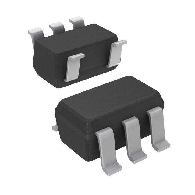
| 产品图片 |
|
| rohs | 符合RoHS无铅 / 符合限制有害物质指令(RoHS)规范要求 |
| 产品系列 | 放大器 IC,运算放大器 - 运放,Texas Instruments TLV2731IDBVRLinCMOS™ |
| 数据手册 | |
| 产品型号 | TLV2731IDBVR |
| 产品目录页面 | |
| 产品种类 | Amplifiers - Operational |
| 供应商器件封装 | SOT-23-5 |
| 共模抑制比—最小值 | 60 dB |
| 关闭 | No Shutdown |
| 其它名称 | 296-10657-1 |
| 包装 | 剪切带 (CT) |
| 单位重量 | 13 mg |
| 压摆率 | 1.6 V/µs |
| 双重电源电压 | +/- 3 V |
| 商标 | Texas Instruments |
| 增益带宽生成 | 2 MHz |
| 增益带宽积 | 2MHz |
| 安装类型 | 表面贴装 |
| 安装风格 | SMD/SMT |
| 封装 | Reel |
| 封装/外壳 | SC-74A,SOT-753 |
| 封装/箱体 | SOT-23-5 |
| 工作温度 | -40°C ~ 85°C |
| 工作电源电压 | 2.7 V to 10 V, +/- 1.35 V to +/- 5 V |
| 工厂包装数量 | 3000 |
| 技术 | LinCMOS |
| 放大器类型 | 通用 |
| 最大双重电源电压 | +/- 5 V |
| 最大工作温度 | + 85 C |
| 最小双重电源电压 | +/- 1.35 V |
| 最小工作温度 | - 40 C |
| 标准包装 | 1 |
| 电压-电源,单/双 (±) | 2.7 V ~ 10 V, ±1.35 V ~ 5 V |
| 电压-输入失调 | 700µV |
| 电流-电源 | 850µA |
| 电流-输入偏置 | 1pA |
| 电流-输出/通道 | 50mA |
| 电源电流 | 1.3 mA |
| 电路数 | 1 |
| 系列 | TLV2731 |
| 转换速度 | 1.6 V/us |
| 输入偏压电流—最大 | 60 pA |
| 输入参考电压噪声 | 100 nV |
| 输入补偿电压 | 3 mV |
| 输出电流 | 50 mA |
| 输出类型 | 满摆幅 |
| 通道数量 | 1 Channel |


- 商务部:美国ITC正式对集成电路等产品启动337调查
- 曝三星4nm工艺存在良率问题 高通将骁龙8 Gen1或转产台积电
- 太阳诱电将投资9.5亿元在常州建新厂生产MLCC 预计2023年完工
- 英特尔发布欧洲新工厂建设计划 深化IDM 2.0 战略
- 台积电先进制程称霸业界 有大客户加持明年业绩稳了
- 达到5530亿美元!SIA预计今年全球半导体销售额将创下新高
- 英特尔拟将自动驾驶子公司Mobileye上市 估值或超500亿美元
- 三星加码芯片和SET,合并消费电子和移动部门,撤换高东真等 CEO
- 三星电子宣布重大人事变动 还合并消费电子和移动部门
- 海关总署:前11个月进口集成电路产品价值2.52万亿元 增长14.8%


PDF Datasheet 数据手册内容提取
TLV2731, TLV2731Y Advanced LinCMOS RAIL-TO-RAIL LOW-POWER SINGLE OPERATIONAL AMPLIFIERS SLOS198A – AUGUST 1997 – REVISED MARCH 2001 (cid:0) Output Swing Includes Both Supply Rails DBV PACKAGE (cid:0) Low Noise...15 nV/√Hz Typ at f = 1 kHz (TOP VIEW) (cid:0) Low Input Bias Current...1 pA Typ OUT 1 5 VDD– /GND (cid:0) Fully Specified for Single-Supply 3-V and 5-V Operation VDD+ 2 (cid:0) Common-Mode Input Voltage Range Includes Negative Rail IN+ 3 4 IN– (cid:0) High Gain Bandwidth...2 MHz at V = 5 V with 600 Ω Load DD (cid:0) High Slew Rate...1.6 V/µs at V = 5 V DD (cid:0) Wide Supply Voltage Range 2.7 V to 10 V (cid:0) Macromodel Included description The TLV2731 is a single low-voltage operational amplifier available in the SOT-23 package. It offers 2 MHz of bandwidth and 1.6 V/µs of slew rate for applications requiring good ac performance. The device exhibits rail-to-rail output performance for increased dynamic range in single or split supply applications. The TLV2731 is fully characterized at 3 V and 5 V and is optimized for low-voltage applications. The TLV2731, exhibiting high input impedance and low noise, is excellent for small-signal conditioning of high-impedance sources, such as piezoelectric transducers. Because of the micropower dissipation levels combined with 3-V operation, these devices work well in hand-held monitoring and remote-sensing applications. In addition, the rail-to-rail output feature with single- or split-supplies makes this family a great choice when interfacing with analog-to-digital converters (ADCs). The device can also drive 600-Ω loads for telecom applications. With a total area of 5.6mm2, the SOT-23 package only requires one-third the board space of the standard 8-pin SOIC package. This ultra-small package allows designers to place single amplifiers very close to the signal source, minimizing noise pick-up from long PCB traces. AVAILABLE OPTIONS PACKAGED DEVICES CHIP TTAA VVIIOOmmaaxx AATT 2255°°CC SSYYMMBBOOLL FFOORRMM‡‡ SOT-23 (DBV)† (Y) 0°C to 70°C 3 mV TLV2731CDBV VALC TTLLVV22773311YY –40°C to 85°C 3 mV TLV2731IDBV VALI †The DBV package available in tape and reel only. ‡Chip forms are tested at TA = 25°C only. Please be aware that an important notice concerning availability, standard warranty, and use in critical applications of TexasInstruments semiconductor products and disclaimers thereto appears at the end of this data sheet. Advanced LinCMOS is a trademark of Texas Instruments. PRODUCTION DATA information is current as of publication date. Copyright 2001, Texas Instruments Incorporated Products conform to specifications per the terms of Texas Instruments standard warranty. Production processing does not necessarily include testing of all parameters. POST OFFICE BOX 655303 • DALLAS, TEXAS 75265 1
TLV2731, TLV2731Y Advanced LinCMOS RAIL-TO-RAIL LOW-POWER SINGLE OPERATIONAL AMPLIFIERS SLOS198A – AUGUST 1997 – REVISED MARCH 2001 TLV2731Y chip information This chip, when properly assembled, displays characteristics similar to the TLV2731C. Thermal compression or ultrasonic bonding may be used on the doped-aluminum bonding pads. This chip may be mounted with conductive epoxy or a gold-silicon preform. BONDING PAD ASSIGNMENTS (5) (1) VDD+ (2) (3) IN+ + (1) OUT (4) IN– – (5) VDD–/GND CHIP THICKNESS: 10 MILS TYPICAL 46 BONDING PADS: 4 × 4 MILS MINIMUM (2) TJmax = 150°C TOLERANCES ARE ±10%. ALL DIMENSIONS ARE IN MILS. PIN (2) IS INTERNALLY CONNECTED TO BACKSIDE OF CHIP. (4) (3) 31 2 POST OFFICE BOX 655303 • DALLAS, TEXAS 75265
TLV2731, TLV2731Y Advanced LinCMOS RAIL-TO-RAIL LOW-POWER SINGLE OPERATIONAL AMPLIFIERS SLOS198A – AUGUST 1997 – REVISED MARCH 2001 equivalent schematic VDD+ Q3 Q6 Q9 Q12 Q14 Q16 R7 C2 IN+ R6 OUT C1 IN– R5 Q1 Q4 Q13 Q15 Q17 R2 D1 Q2 Q5 Q7 Q8 Q10 Q11 R3 R4 R1 VDD–/GND COMPONENT COUNT† Transistors 23 Diodes 5 Resistors 11 Capacitors 2 †Includes both amplifiers and all ESD, bias, and trim circuitry POST OFFICE BOX 655303 • DALLAS, TEXAS 75265 3
TLV2731, TLV2731Y Advanced LinCMOS RAIL-TO-RAIL LOW-POWER SINGLE OPERATIONAL AMPLIFIERS SLOS198A – AUGUST 1997 – REVISED MARCH 2001 absolute maximum ratings over operating free-air temperature range (unless otherwise noted)† Supply voltage, V (see Note 1) . . . . . . . . . . . . . . . . . . . . . . . . . . . . . . . . . . . . . . . . . . . . . . . . . . . . . . . . . . . . 12 V DD Differential input voltage, V (see Note 2) . . . . . . . . . . . . . . . . . . . . . . . . . . . . . . . . . . . . . . . . . . . . . . . . . . . ±V ID DD Input voltage range, V (any input, see Note 1) . . . . . . . . . . . . . . . . . . . . . . . . . . . . . . . . . . . . . . . . –0.3 V to V I DD Input current, I (each input) . . . . . . . . . . . . . . . . . . . . . . . . . . . . . . . . . . . . . . . . . . . . . . . . . . . . . . . . . . . . . . . ±5 mA I Output current, I . . . . . . . . . . . . . . . . . . . . . . . . . . . . . . . . . . . . . . . . . . . . . . . . . . . . . . . . . . . . . . . . . . . . . . . ±50 mA O Total current into V . . . . . . . . . . . . . . . . . . . . . . . . . . . . . . . . . . . . . . . . . . . . . . . . . . . . . . . . . . . . . . . . . . ±50 mA DD+ Total current out of V . . . . . . . . . . . . . . . . . . . . . . . . . . . . . . . . . . . . . . . . . . . . . . . . . . . . . . . . . . . . . . . . ±50 mA DD– Duration of short-circuit current (at or below) 25°C (see Note 3) . . . . . . . . . . . . . . . . . . . . . . . . . . . . . . unlimited Continuous total power dissipation . . . . . . . . . . . . . . . . . . . . . . . . . . . . . . . . . . . . . See Dissipation Rating Table Operating free-air temperature range, T : TLV2731C . . . . . . . . . . . . . . . . . . . . . . . . . . . . . . . . . . . 0°C to 70°C A TLV2731I . . . . . . . . . . . . . . . . . . . . . . . . . . . . . . . . . . –40°C to 85°C Storage temperature range, T . . . . . . . . . . . . . . . . . . . . . . . . . . . . . . . . . . . . . . . . . . . . . . . . . . . –65°C to 150°C stg Lead temperature 1,6 mm (1/16 inch) from case for 10 seconds: DBV package . . . . . . . . . . . . . . . . . . 260°C †Stresses beyond those listed under “absolute maximum ratings” may cause permanent damage to the device. These are stress ratings only, and functional operation of the device at these or any other conditions beyond those indicated under “recommended operating conditions” is not implied. Exposure to absolute-maximum-rated conditions for extended periods may affect device reliability. NOTES: 1. All voltage values, except differential voltages, are with respect to VDD–. 2. Differential voltages are at the noninverting input with respect to the inverting input. Excessive current flows when input is brought below VDD– – 0.3 V. 3. The output may be shorted to either supply. Temperature and/or supply voltages must be limited to ensure that the maximum dissipation rating is not exceeded. DISSIPATION RATING TABLE PPAACCKKAAGGEE TAA ≤ 25°C DERATING FACTOR TAA = 70°C TAA = 85°C POWER RATING ABOVE TA = 25°C POWER RATING POWER RATING DBV 150 mW 1.2 mW/°C 96 mW 78 mW recommended operating conditions TLV2731C TLV2731I UUNNIITT MIN MAX MIN MAX Supply voltage, VDD(cid:1)(cid:7)(cid:5)(cid:5)(cid:4)(cid:6)(cid:8)(cid:5)(cid:3)(cid:2) 2.7 10 2.7 10 V Input voltage range, VI VDD– VDD+ –1.3 VDD– VDD+ –1.3 V Common-mode input voltage, VIC VDD– VDD+ –1.3 VDD– VDD+ –1.3 V Operating free-air temperature, TA 0 70 –40 85 °C NOTE 1: All voltage values, except differential voltages, are with respect to VDD–. 4 POST OFFICE BOX 655303 • DALLAS, TEXAS 75265
TLV2731, TLV2731Y Advanced LinCMOS RAIL-TO-RAIL LOW-POWER SINGLE OPERATIONAL AMPLIFIERS SLOS198A – AUGUST 1997 – REVISED MARCH 2001 electrical characteristics at specified free-air temperature, V = 3 V (unless otherwise noted) DD TLV2731C TLV2731I PPAARRAAMMEETTEERR TTEESSTT CCOONNDDIITTIIOONNSS TTAA†† UUNNIITT MIN TYP MAX MIN TYP MAX VIO Input offset voltage 0.7 3 0.7 3 mV Temperature Full range ααVVIIOO ccooeeffffiicciieenntt ooff iinnppuutt 00.55 00.55 µµVV//°°CC offset voltage Input offset voltage long-term drift VVVVDD± = ±1.5 VVVV, VVVVIC = 0, 25°C 0.003 0.003 µV/mo (see Note 4) VO = 0, RS = 50 Ω 25°C 0.5 60 0.5 60 IIIIOO IInnppuutt ooffffsseett ccuurrrreenntt ppAA Full range 150 150 25°C 1 60 1 60 IIIIBB IInnppuutt bbiiaass ccuurrrreenntt ppAA Full range 150 150 ––00.33 ––00.33 2255°CC 00 ttoo 22 00 ttoo 22 ttoo 22.22 ttoo 22.22 Common-mode input VVIICCRR RRSS == 5500 ΩΩ, ||VVIIOO|| ≤≤55 mmVV VV vvoollttaaggee rraannggee 00 ttoo 00 ttoo FFuullll rraannggee 11.77 11.77 IOH = –1 mA 25°C 2.87 2.87 HHiighh-llevell outtputt VOH 25°C 2.74 2.74 V vvoollttaaggee IIOOHH == –22 mmAA Full range 2.3 2.3 VIC = 1.5 V, IOL = 50 µA 25°C 10 10 LLow-llevell outtputt VOL 25°C 100 100 mV vvoollttaaggee VVIICC == 11.55 VV, IIOOLL == 550000 µµAA Full range 300 300 25°C 1 1.6 1 1.6 AVVDD LLdaaiffrreggreee-nsstiiiggannl aavlloltage VVVVIOOC === 1111 .VV55 ttVVoo, 22 VV RRL = 660000 ΩΩ‡‡ Full range 0.3 0.3 V/mV amplification RL = 1 MΩ‡ 25°C 250 250 Differential input rid resistance 25°C 1012 1012 Ω Common-mode input ric resistance 25°C 1012 1012 Ω Common-mode input cic capacitance f = 10 kHz 25°C 6 6 pF Closed-loop output zo impedance f = 1 MHz, AV = 1 25°C 156 156 Ω CCMMRRRR Creojemcmtioonn r-amtioode VVOIICC == 10. 5to V 1, .7 V,, RS = 50Ω Fu2ll 5ra°Cnge 6505 70 6505 70 ddBB Supply voltage 25°C 70 96 70 96 kkSSVVRR rreejjeeccttiioonn rraattiioo VDDDD = 2.7 V to 8 V,, ddBB (∆VDD /∆VIO) VIC = VDD/2, No load Full range 70 70 25°C 750 1200 750 1200 IIDDDD SSuuppppllyy ccuurrrreenntt VVOO == 11.55 VV, NNoo llooaadd µµAA Full range 1500 1500 †Full range for the TLV2731C is 0°C to 70°C. Full range for the TLV2731I is – 40°C to 85°C. ‡Referenced to 1.5 V NOTE 4: Typical values are based on the input offset voltage shift observed through 500 hours of operating life test at TA = 150°C extrapolated to TA = 25°C using the Arrhenius equation and assuming an activation energy of 0.96 eV. POST OFFICE BOX 655303 • DALLAS, TEXAS 75265 5
TLV2731, TLV2731Y Advanced LinCMOS RAIL-TO-RAIL LOW-POWER SINGLE OPERATIONAL AMPLIFIERS SLOS198A – AUGUST 1997 – REVISED MARCH 2001 operating characteristics at specified free-air temperature, V = 3 V DD TLV2731C TLV2731I PPAARRAAMMEETTEERR TTEESSTT CCOONNDDIITTIIOONNSS TTAA†† UUNNIITT MIN TYP MAX MIN TYP MAX 25°C 0.75 1.25 0.75 1.25 SR SSlleeww rraattee aatt uunniittyy VO = 1.1 V to 1.9 V, RL = 600 Ω‡‡, Full V/µs gain CL = 100 pF‡ range 0.5 0.5 Eqquivalent input f = 10 Hz 25°C 105 105 VVn nnVV//√√HHzz noise voltage f = 1 kHz 25°C 16 16 Peak-to-peak f = 0.1 Hz to 1 Hz 25°C 1.4 1.4 VVNN((PPPP)) eeqquuiivvaalleenntt iinnppuutt µµVV noise voltage f = 0.1 Hz to 10 Hz 25°C 1.5 1.5 Equivalent input In noise current 25°C 0.6 0.6 fA/√Hz VO = 1 V to 2 V, AV = 1 0.285% 0.285% ff = 2200 kkHHzz, 2255°°CC Total harmonic RL = 600 Ω‡ AV = 10 7.2% 7.2% THD+N distortion plus nnooiissee VVOO == 11 VV ttoo 22 VV,, AV = 1 0.014% 0.014% f = 20 kHz, AV = 10 25°C 0.098% 0.098% RL = 600 Ω§§ AV = 100 0.13% 0.13% Gain-bandwidth f = 10 kHz, RL = 600 Ω‡, 25°C 1.9 1.9 MHz product CL = 100 pF‡ BOM Mswaixnigm buamn dowutipdutht- VROL (=P 6P0) 0= Ω1‡ V,, ACVL == 11,00 pF‡ 25°C 60 60 kHz AV = –1, To 0.1% 0.9 0.9 tts SSeettttlliinngg ttiimmee SRtLe p= =6 010 V Ω t‡o, 2 V,, 2255°°CC µµss CL = 100 pF‡ To 0.01% 1.5 1.5 Phase margin at φm unity gain RLL = 600 Ω‡,, CLL = 100 pF‡ 25°C 50° 50° Gain margin 25°C 8 8 dB †Full range is –40°C to 85°C. ‡Referenced to 1.5 V §Referenced to 0 V 6 POST OFFICE BOX 655303 • DALLAS, TEXAS 75265
TLV2731, TLV2731Y Advanced LinCMOS RAIL-TO-RAIL LOW-POWER SINGLE OPERATIONAL AMPLIFIERS SLOS198A – AUGUST 1997 – REVISED MARCH 2001 electrical characteristics at specified free-air temperature, V = 5 V (unless otherwise noted) DD TLV2731C TLV2731I PPAARRAAMMEETTEERR TTEESSTT CCOONNDDIITTIIOONNSS TTAA†† UUNNIITT MIN TYP MAX MIN TYP MAX VIO Input offset voltage 0.7 3 0.7 3 mV Temperature Full range ααVVIIOO ccooeeffffiicciieenntt ooff iinnppuutt 00.55 00.55 µµVV//°°CC offset voltage Input offset voltage long-term drift VVVVDD± = ±2.5 VVVV, VVVVIC = 0, 25°C 0.003 0.003 µV/mo (see Note 4) VO = 0, RS = 50 Ω 25°C 0.5 60 0.5 60 IIIIOO IInnppuutt ooffffsseett ccuurrrreenntt ppAA Full range 150 150 25°C 1 60 1 60 IIIIBB IInnppuutt bbiiaass ccuurrrreenntt ppAA Full range 150 150 ––00.33 ––00.33 2255°CC 00 ttoo 44 00 ttoo 44 ttoo 44.22 ttoo 44.22 Common-mode input VVIICCRR RRSS == 5500 ΩΩ, ||VVIIOO|| ≤≤55 mmVV VV vvoollttaaggee rraannggee 00 ttoo 00 ttoo FFuullll rraannggee 33.77 33.77 IOH = –1 mA 25°C 4.9 4.9 HHiighh-llevell outtputt VOH 25°C 4.6 4.6 V vvoollttaaggee IIOOHH == –44 mmAA Full range 4.3 4.3 VIC = 2.5 V, IOL = 500 µA 25°C 80 80 LLow-llevell outtputt VOL 25°C 160 160 mV vvoollttaaggee VVIICC == 22.55 VV, IIOOLL == 11 mmAA Full range 500 500 25°C 1 1.5 1 1.5 AVVDD LLdaaiffrreggreee-nsstiiiggannl aavlloltage VVVVIOOC === 1122 .VV55 ttVVoo, 44 VV RRL = 660000 ΩΩ‡‡ Full range 0.3 0.3 V/mV amplification RL = 1 MΩ‡ 25°C 400 400 Differential input rid resistance 25°C 1012 1012 Ω Common-mode input ric resistance 25°C 1012 1012 Ω Common-mode input cic capacitance f = 10 kHz 25°C 6 6 pF Closed-loop output zo impedance f = 1 MHz, AV = 1 25°C 138 138 Ω CCMMRRRR Creojemcmtioonn r-amtioode VVOIICC == 20. 5to V 2, .7 V,, RS = 50Ω Fu2ll 5ra°Cnge 6505 70 6505 70 ddBB Supply voltage 25°C 70 96 70 96 kkSSVVRR rreejjeeccttiioonn rraattiioo VDDDD = 4.4 V to 8 V,, ddBB (∆VDD /∆VIO) VIC = VDD/2, No load Full range 70 70 25°C 850 1300 850 1300 IIDDDD SSuuppppllyy ccuurrrreenntt VVOO == 22.55 VV, NNoo llooaadd µµAA Full range 1600 1600 †Full range for the TLV2731C is 0°C to 70°C. Full range for the TLV2731I is – 40°C to 85°C. ‡Referenced to 2.5 V NOTE 5: Typical values are based on the input offset voltage shift observed through 500 hours of operating life test at TA = 150°C extrapolated to TA = 25°C using the Arrhenius equation and assuming an activation energy of 0.96 eV. POST OFFICE BOX 655303 • DALLAS, TEXAS 75265 7
TLV2731, TLV2731Y Advanced LinCMOS RAIL-TO-RAIL LOW-POWER SINGLE OPERATIONAL AMPLIFIERS SLOS198A – AUGUST 1997 – REVISED MARCH 2001 operating characteristics at specified free-air temperature, V = 5 V DD TLV2731C TLV2731I PPAARRAAMMEETTEERR TTEESSTT CCOONNDDIITTIIOONNSS TTAA†† UUNNIITT MIN TYP MAX MIN TYP MAX 25°C 1 1.6 1 1.6 SR SSgalleeinww rraattee aatt uunniittyy VVCOOL === 1110.550 VVpF ttoo‡ 33.55 VV, RRL = 660000 ΩΩ‡‡, Full 0.7 0.7 V/µs range Eqquivalent input f = 10 Hz 25°C 100 100 VVn nnVV//√√HHzz noise voltage f = 1 kHz 25°C 15 15 Peak-to-peak f = 0.1 Hz to 1 Hz 25°C 1.4 1.4 VVNN((PPPP)) eeqquuiivvaalleenntt iinnppuutt µµVV noise voltage f = 0.1 Hz to 10 Hz 25°C 1.5 1.5 Equivalent input In noise current 25°C 0.6 0.6 fA/√Hz VO = 1.5 V to 3.5 V, AV = 1 0.409% 0.409% ff = 2200 kkHHzz, 2255°°CC Total harmonic RL = 600 Ω‡ AV = 10 3.68% 3.68% THD+N distortion plus nnooiissee VVOO == 11..55 VV ttoo 33..55 VV,, AV = 1 0.018% 0.018% f = 20 kHz, AV = 10 25°C 0.045% 0.045% RL = 600 Ω§§ AV = 100 0.116% 0.116% Gain-bandwidth f = 10 kHz, RL = 600 Ω‡, 25°C 2 2 MHz product CL = 100 pF‡ Maximum BOM output-swing VROL (=P 6P0) 0= Ω1‡ V,, ACVL == 11,00 pF‡ 25°C 300 300 kHz bandwidth AV = –1, To 0.1% 0.95 0.95 tts SSeettttlliinngg ttiimmee SRtLe p= =6 010.5 Ω V‡ ,to 3.5 V,, 2255°°CC µµss CL = 100 pF‡ To 0.01% 2.4 2.4 Phase margin at φm unity gain RLL = 600 Ω‡,, CLL = 100 pF‡ 25°C 48° 48° Gain margin 25°C 8 8 dB †Full range is –40°C to 85°C. ‡Referenced to 2.5 V §Referenced to 0 V 8 POST OFFICE BOX 655303 • DALLAS, TEXAS 75265
TLV2731, TLV2731Y Advanced LinCMOS RAIL-TO-RAIL LOW-POWER SINGLE OPERATIONAL AMPLIFIERS SLOS198A – AUGUST 1997 – REVISED MARCH 2001 electrical characteristics at V = 3 V, T = 25°C (unless otherwise noted) DD A TLV2731Y PPAARRAAMMEETTEERR TTEESSTT CCOONNDDIITTIIOONNSS UUNNIITT MIN TYP MAX VIO Input offset voltage 750 µV IIO Input offset current VVRRDSSD ==±± 55 =00 ΩΩ±±11.55 VV, VVIC = 00, VVO = 00, 0.5 60 pA IIB Input bias current 1 60 pA –0.3 VIICCRR Common-mode input voltagge rangge |VIIOO| ≤5 mV, RSS = 50 Ω to V 2.2 VOH High-level output voltage IOH = –1 mA 2.87 V VIC = 1.5 V, IOL = 50 µA 10 VVOOLL LLooww-lleevveell oouuttppuutt vvoollttaaggee mmVV VIC = 1.5 V, IOL = 500 µA 100 RL = 600 Ω† 1.6 AAVVDD LLaarrggee-ssiiggnnaall ddiiffffeerreennttiiaall vvoollttaaggee aammpplliiffiiccaattiioonn VVOO == 11 VV ttoo 22 VV VV//mmVV RL = 1 MΩ† 250 rid Differential input resistance 1012 Ω ric Common-mode input resistance 1012 Ω cic Common-mode input capacitance f = 10 kHz 6 pF zo Closed-loop output impedance f = 1 MHz, AV = 1 156 Ω CMRR Common-mode rejection ratio VIC = 0 to 1.7 V, VO = 0, RS = 50 Ω 70 dB kkSSVVRR SSuuppppllyy vvoollttaaggee rreejjeeccttiioonn rraattiioo ((∆∆VVDDDD//∆∆VVIIOO)) VVDDDD = 22.77 VV ttoo 88 VV, VVIICC = 00, NNoo llooaadd 9966 ddBB IDD Supply current VO = 0, No load 750 µA †Referenced to 1.5 V electrical characteristics at V = 5 V, T = 25°C (unless otherwise noted) DD A TLV2731Y PPAARRAAMMEETTEERR TTEESSTT CCOONNDDIITTIIOONNSS UUNNIITT MIN TYP MAX VIO Input offset voltage 710 µV IIO Input offset current VVRRDSSD ==±± 55 =00 ΩΩ±±11.55 VV, VVIC = 00, VVO = 00, 0.5 60 pA IIB Input bias current 1 60 pA –0.3 VIICCRR Common-mode input voltagge rangge |VIIOO| ≤5 mV, RSS = 50 Ω to V 4.2 VOH High-level output voltage IOH = –1 mA 4.9 V VIC = 2.5 V, IOL = 500 µA 80 VVOOLL LLooww-lleevveell oouuttppuutt vvoollttaaggee mmVV VIC = 2.5 V, IOL = 1 mA 160 RL = 600 Ω† 15 AAVVDD LLaarrggee-ssiiggnnaall ddiiffffeerreennttiiaall vvoollttaaggee aammpplliiffiiccaattiioonn VVOO == 11 VV ttoo 22 VV VV//mmVV RL = 1 MΩ† 400 rid Differential input resistance 1012 Ω ric Common-mode input resistance 1012 Ω cic Common-mode input capacitance f = 10 kHz 6 pF zo Closed-loop output impedance f = 1 MHz, AV = 1 138 Ω CMRR Common-mode rejection ratio VIC = 0 to 1.7 V, VO = 0, RS = 50 Ω 70 dB kkSSVVRR SSuuppppllyy vvoollttaaggee rreejjeeccttiioonn rraattiioo ((∆∆VVDDDD//∆∆VVIIOO)) VVDDDD = 22.77 VV ttoo 88 VV, VVIICC = 00, NNoo llooaadd 9966 ddBB IDD Supply current VO = 0, No load 850 µA †Referenced to 2.5 V POST OFFICE BOX 655303 • DALLAS, TEXAS 75265 9
TLV2731, TLV2731Y Advanced LinCMOS RAIL-TO-RAIL LOW-POWER SINGLE OPERATIONAL AMPLIFIERS SLOS198A – AUGUST 1997 – REVISED MARCH 2001 TYPICAL CHARACTERISTICS Table of Graphs FIGURE Distribution 1,, 2 VVIIOO IInnppuutt ooffffsseett vvoollttaaggee vs Common-mode input voltage 3, 4 αVIO Input offset voltage temperature coefficient Distribution 5, 6 IIB/IIO Input bias and input offset currents vs Free-air temperature 7 vs Supplyy voltagge 8 VVII IInnppuutt vvoollttaaggee vs Free-air temperature 9 VOH High-level output voltage vs High-level output current 10, 13 VOL Low-level output voltage vs Low-level output current 11, 12, 14 VO(PP) Maximum peak-to-peak output voltage vs Frequency 15 vs Supplyy voltagge 16 IIOOSS SShhoorrtt-cciirrccuuiitt oouuttppuutt ccuurrrreenntt vs Free-air temperature 17 VO Output voltage vs Differential input voltage 18, 19 AVD Differential voltage amplification vs Load resistance 20 vs Freqquencyy 21,, 22 AAVVDD LLaarrggee-ssiiggnnaall ddiiffffeerreennttiiaall vvoollttaaggee aammpplliiffiiccaattiioonn vs Free-air temperature 23, 24 zo Output impedance vs Frequency 25, 26 vs Freqquencyy 27 CCMMRRRR CCoommmmoonn-mmooddee rreejjeeccttiioonn rraattiioo vs Free-air temperature 28 vs Freqquencyy 29,, 30 kkSSVVRR SSuuppppllyy-vvoollttaaggee rreejjeeccttiioonn rraattiioo vs Free-air temperature 31 IDD Supply current vs Supply voltage 32 vs Load capacitance 33 SSRR SSlleeww rraattee vs Free-air temperature 34 VO Inverting large-signal pulse response 35, 36 VO Voltage-follower large-signal pulse response 37, 38 VO Inverting small-signal pulse response 39, 40 VO Voltage-follower small-signal pulse response 41, 42 Vn Equivalent input noise voltage vs Frequency 43, 44 Noise voltage (referred to input) Over a 10-second period 45 THD + N Total harmonic distortion plus noise vs Frequency 46 vs Free-air temperature 47 GGaaiinn-bbaannddwwiiddtthh pprroodduucctt vs Supply voltage 48 Gain margin vs Load capacitance 49, 50 vs Freqquencyy 21,, 22 φφm PPhhaassee mmaarrggiinn vs Load capacitance 51, 52 B1 Unity-gain bandwidth vs Load capacitance 53, 54 10 POST OFFICE BOX 655303 • DALLAS, TEXAS 75265
TLV2731, TLV2731Y Advanced LinCMOS RAIL-TO-RAIL LOW-POWER SINGLE OPERATIONAL AMPLIFIERS SLOS198A – AUGUST 1997 – REVISED MARCH 2001 TYPICAL CHARACTERISTICS DISTRIBUTION OF TLV2731 DISTRIBUTION OF TLV2731 INPUT OFFSET VOLTAGE INPUT OFFSET VOLTAGE 20 16 537 Amplifiers From 1 Wafer Lot 537 Amplifiers 18 VDD = ±1.5 V 14 From 1 Wafer Lot TA = 25°C VDD = ±2.5 V 16 TA = 25°C % % 12 s – 14 s – er er 10 plifi 12 plifi m m A 10 A 8 of of age 8 age 6 nt nt e 6 e ec ec 4 Pr 4 Pr 2 2 0 0 3 6 2 8 4 1 6 2 2 6 1 4 8 2 6 3 –3 2.6 2.2 1.8 1.4 –1 0.6 0.2 0.2 0.6 1 1.4 1.8 2.2 2.6 3 – –2. –2. –1. –1. – –0. –0. 0. 0. 1. 1. 2. 2. – – – – – – VIO – Input Offset Voltage – mV VIO – Input Offset Voltage – mV Figure 1 Figure 2 INPUT OFFSET VOLTAGE† INPUT OFFSET VOLTAGE† vs vs COMMON-MODE INPUT VOLTAGE COMMON-MODE INPUT VOLTAGE 1 1 VDD = 3 V VDD = 5 V 0.8 RS = 50 Ω 0.8 RS = 50 Ω TA = 25°C TA = 25°C 0.6 0.6 V V m m 0.4 – 0.4 age – 0.2 oltage 0.2 Volt 0 et V 0 Offset –0.2 ut Offs –0.2 ut –0.4 ÁnpÁ–0.4 np – I Á– IÁ–0.6 ÁOÁ–0.6 O VI ÁVIÁ ÁÁ –0.8 –0.8 –1 –1 –1 0 1 2 3 –1 0 1 2 3 4 5 VIC – Common-Mode Input Voltage – V VIC – Common-Mode Input Voltage – V Figure 3 Figure 4 †For all curves where VDD = 5 V, all loads are referenced to 2.5 V. For all curves where VDD = 3 V, all loads are referenced to 1.5 V. POST OFFICE BOX 655303 • DALLAS, TEXAS 75265 11
TLV2731, TLV2731Y Advanced LinCMOS RAIL-TO-RAIL LOW-POWER SINGLE OPERATIONAL AMPLIFIERS SLOS198A – AUGUST 1997 – REVISED MARCH 2001 TYPICAL CHARACTERISTICS DISTRIBUTION OF TLV2731 INPUT OFFSET DISTRIBUTION OF TLV2731 INPUT OFFSET VOLTAGE TEMPERATURE COEFFICIENT† VOLTAGE TEMPERATURE COEFFICIENT† 30 30 32 Amplifiers From 32 Amplifiers From 1 Wafer Lots 1 Wafer Lots 25 VDD± = ±1.5 V 25 VDD± = ±2.5 V P Package P Package – % TA = 25°C to 125°C – % TA = 25°C to 125°C s s r 20 r 20 e e plifi plifi m m A 15 A 15 of of e e g g a a nt 10 nt 10 e e c c r r e e P P 5 5 0 0 –4 –3 –2 –1 0 1 2 3 4 –4 –3 –2 –1 0 1 2 3 4 αVIO – Input Offset Voltage αVIO – Input Offset Voltage Temperature Coefficient – µV/°C Temperature Coefficient – µV/°C Figure 5 Figure 6 INPUT BIAS AND INPUT OFFSET CURRENTS† INPUT VOLTAGE vs vs FREE-AIR TEMPERATURE SUPPLY VOLTAGE A p 100 5 s – VDD± = ±2.5 V RS = 50 Ω nt 90 VIC = 0 4 TA = 25°C re VO = 0 Cur 80 RS = 50 Ω 3 et s 70 2 Off – V ut 60 e 1 p g n a ut Bias and I 435000 Á– Input Volt Á––120 |VIO| ≤5 mV p VI n ÁÁ – I 20 –3 d IIO IIO 10 IIB IIO –4 n a B B 0 –5 IIII 25 45 65 85 105 125 1 1.5 2 2.5 3 3.5 4 TA – Free-Air Temperature – °C |VDD±| – Supply Voltage – V Figure 7 Figure 8 †Data at high and low temperatures are applicable only within the rated operating free-air temperature ranges of the various devices. 12 POST OFFICE BOX 655303 • DALLAS, TEXAS 75265
TLV2731, TLV2731Y Advanced LinCMOS RAIL-TO-RAIL LOW-POWER SINGLE OPERATIONAL AMPLIFIERS SLOS198A – AUGUST 1997 – REVISED MARCH 2001 TYPICAL CHARACTERISTICS INPUT VOLTAGE† HIGH-LEVEL OUTPUT VOLTAGE†‡ vs vs FREE-AIR TEMPERATURE HIGH-LEVEL OUTPUT CURRENT 5 3 VDD = 5 V VDD = 3 V 4 2.5 – V TA = –40°C e g V 3 a 2 – olt TA = 25°C e V ag ut Á– Input VoltÁ 21 |VIO| ≤5 mV h-Level Outp 1.15 TA = 85°C VI ÁÁHig TA = 125°C 0 – 0.5 H ÁÁO V –1 0 –55 –35 –15 5 25 45 65 85 105 125 0 5 10 15 TA – Free-Air Temperature – °C |IOH| – High-Level Output Current – mA Figure 9 Figure 10 LOW-LEVEL OUTPUT VOLTAGE‡ LOW-LEVEL OUTPUT VOLTAGE†‡ vs vs LOW-LEVEL OUTPUT CURRENT LOW-LEVEL OUTPUT CURRENT 1.2 1.4 VDD = 3 V VDD = 3 V TA = 25°C VIC = 1.5 V 1.2 1 V – V VIC = 0 e – TA = 125°C ge ag 1 olta 0.8 Volt TA = 85°C ut V VIC = 0.75 V put 0.8 utp 0.6 Out TA = 25°C ow-Level O 0.4 VIC = 1.5 V ÁÁLow-Level 00..46 TA = –40°C L – Á– LÁ0.2 ÁÁOL O V 0.2 ÁVÁ ÁÁ 0 0 0 1 2 3 4 5 0 1 2 3 4 5 IOL – Low-Level Output Current – mA IOL – Low-Level Output Current – mA Figure 11 Figure 12 †Data at high and low temperatures are applicable only within the rated operating free-air temperature ranges of the various devices. ‡For all curves where VDD = 5 V, all loads are referenced to 2.5 V. For all curves where VDD = 3 V, all loads are referenced to 1.5 V. POST OFFICE BOX 655303 • DALLAS, TEXAS 75265 13
TLV2731, TLV2731Y Advanced LinCMOS RAIL-TO-RAIL LOW-POWER SINGLE OPERATIONAL AMPLIFIERS SLOS198A – AUGUST 1997 – REVISED MARCH 2001 TYPICAL CHARACTERISTICS HIGH-LEVEL OUTPUT VOLTAGE†‡ LOW-LEVEL OUTPUT VOLTAGE†‡ vs vs HIGH-LEVEL OUTPUT CURRENT LOW-LEVEL OUTPUT CURRENT 5 1.4 VDD = 5 V VDD = 5 V 4.5 VIC = 2.5 V 1.2 – V 4 TA = –40°C V TA = 125°C e – ag 3.5 ge 1 put Volt 3 TA = 25°C ut Volta 0.8 TA = 85°C Out 2.5 utp TA = 25°C vel 2 TA = 85°C el O 0.6 e v gh-L 1.5 w-Le 0.4 TA = –40°C Hi TA = 125°C o ÁÁ– 1 Á– L Á H ÁÁVO 0.5 ÁVOLÁ0.2 0 0 0 5 10 15 20 25 30 0 1 2 3 4 5 6 |IOH| – High-Level Output Current – mA IOL – Low-Level Output Current – mA Figure 13 Figure 14 MAXIMUM PEAK-TO-PEAK OUTPUT VOLTAGE‡ SHORT-CIRCUIT OUTPUT CURRENT vs vs FREQUENCY SUPPLY VOLTAGE ge – V 5 RTAI == 62050° CΩ 3205 VO = VDD/2 Output Volta 4 VDD = 5 V urrent – mA 211050 VTAIC = = 2 V5D°CD/2 VID = –100 mV eak 3 ut C 5 P p m Peak-to- 2 VDD = 3 V Circuit Out ––1050 mu rt- o xi h –15 Á– MaPP)Á1 I– SOS ––2205 VID = 100 mV ÁVO(Á0 –30 ÁÁ 102 103 104 105 106 2 3 4 5 6 7 8 f – Frequency – Hz VDD – Supply Voltage – V Figure 15 Figure 16 †Data at high and low temperatures are applicable only within the rated operating free-air temperature ranges of the various devices. ‡For all curves where VDD = 5 V, all loads are referenced to 2.5 V. For all curves where VDD = 3 V, all loads are referenced to 1.5 V. 14 POST OFFICE BOX 655303 • DALLAS, TEXAS 75265
TLV2731, TLV2731Y Advanced LinCMOS RAIL-TO-RAIL LOW-POWER SINGLE OPERATIONAL AMPLIFIERS SLOS198A – AUGUST 1997 – REVISED MARCH 2001 TYPICAL CHARACTERISTICS SHORT-CIRCUIT OUTPUT CURRENT†‡ OUTPUT VOLTAGE‡ vs vs FREE-AIR TEMPERATURE DIFFERENTIAL INPUT VOLTAGE 30 3 VDD = 5 V VDD = 3 V nt – mA 221505 VVIOC == 22..55 VV 2.5 RTVAIIC == = 62 0150.°5 CΩ V e V Curr 10 VID = –100 mV e – 2 put 5 oltag ut V rcuit O –05 Output 1.5 rt-Ci –10 – O 1 o V h –15 VID = 100 mV S – S –20 0.5 O I –25 –30 0 –75 –50 –25 0 25 50 75 100 125 –10 –8 –6 –4 –2 0 2 4 6 8 10 TA – Free-Air Temperature – °C VID – Differential Input Voltage – mV Figure 17 Figure 18 OUTPUT VOLTAGE‡ DIFFERENTIAL VOLTAGE AMPLIFICATION‡ vs vs DIFFERENTIAL INPUT VOLTAGE LOAD RESISTANCE 5 104 VDD = 5 V mV VO(PP) = 2 V 4 RVILC = = 6 20.05 ΩV n – V/ TA = 25°C TA = 25°C atio 103 ge – V 3 mplific VDD = 5 V a A Volt ge 102 VDD = 3 V Output 2 al Volta – nti VO ere 101 1 ÁDiffÁ – ÁDÁ V A 0 ÁÁ1 –10 –8 –6 –4 –2 0 2 4 6 8 10 0.1 1 101 102 103 VID – Differential Input Voltage – mV RL – Load Resistance – kΩ Figure 19 Figure 20 †Data at high and low temperatures are applicable only within the rated operating free-air temperature ranges of the various devices. ‡For all curves where VDD = 5 V, all loads are referenced to 2.5 V. For all curves where VDD = 3 V, all loads are referenced to 1.5 V. POST OFFICE BOX 655303 • DALLAS, TEXAS 75265 15
TLV2731, TLV2731Y Advanced LinCMOS RAIL-TO-RAIL LOW-POWER SINGLE OPERATIONAL AMPLIFIERS SLOS198A – AUGUST 1997 – REVISED MARCH 2001 TYPICAL CHARACTERISTICS LARGE-SIGNAL DIFFERENTIAL VOLTAGE AMPLIFICATION AND PHASE MARGIN† vs FREQUENCY 80 180° VDD = 3 V RL = 600 Ω 60 CL= 100 pF 135° al TA = 25°C nti dB al Differe cation – 40 Phase Margin 90° Margin rge-Sign e Amplifi 20 Gain 45° – Phase La ag 0 0° m m ÁÁD – DVolt φo ÁÁAVAV –20 –45° –40 –90° 104 105 106 107 f – Frequency – Hz Figure 21 LARGE-SIGNAL DIFFERENTIAL VOLTAGE AMPLIFICATION AND PHASE MARGIN† vs FREQUENCY 80 180° VDD = 5 V RL= 600 Ω 60 CL= 100 pF 135° al TA = 25°C nti dB al Differe cation – 40 Phase Margin 90° Margin Large-Sign age Amplifi 200 Gain 04°5° m – Phase m ÁÁD – DVolt φo VV ÁÁAA –20 –45° –40 –90° 104 105 106 107 f – Frequency – Hz Figure 22 †For all curves where VDD = 5 V, all loads are referenced to 2.5 V. For all curves where VDD = 3 V, all loads are referenced to 1.5 V. 16 POST OFFICE BOX 655303 • DALLAS, TEXAS 75265
TLV2731, TLV2731Y Advanced LinCMOS RAIL-TO-RAIL LOW-POWER SINGLE OPERATIONAL AMPLIFIERS SLOS198A – AUGUST 1997 – REVISED MARCH 2001 TYPICAL CHARACTERISTICS LARGE-SIGNAL DIFFERENTIAL LARGE-SIGNAL DIFFERENTIAL VOLTAGE AMPLIFICATION†‡ VOLTAGE AMPLIFICATION†‡ vs vs FREE-AIR TEMPERATURE FREE-AIR TEMPERATURE 103 103 Voltage 102 RL = 1 MΩ Voltage 102 RL = 1 MΩ Differential n – V/mV 101 Differential n – V/mV 101 – Large-Signal Amplificatio 1 VDD = 3 V RL = 600 Ω – Large-Signal Amplificatio 1 VDD = 5 V RL = 600 Ω VD VIC = 1.5 V VD VIC = 2.5 V A VO = 0.5 V to 2.5 V A VO = 1 V to 4 V 0.1 0.1 –75 –50 –25 0 25 50 75 100 125 –75 –50 –25 0 25 50 75 100 125 TA – Free-Air Temperature – °C TA – Free-Air Temperature – °C Figure 23 Figure 24 OUTPUT IMPEDANCE‡ OUTPUT IMPEDANCE‡ vs vs FREQUENCY FREQUENCY 1000 1000 VDD = 3 V VDD = 5 V TA = 25°C TA = 25°C Ωmpedance – 10100 AV = 100 Ωmpedance – 10100 AV = 100 – Output Izo 1 AV = 10 – Output Io 1 AV = 10 z AV = 1 AV = 1 0.1 0.1 102 103 104 105 106 102 103 104 105 106 f– Frequency – Hz f– Frequency – Hz Figure 25 Figure 26 †Data at high and low temperatures are applicable only within the rated operating free-air temperature ranges of the various devices. ‡For all curves where VDD = 5 V, all loads are referenced to 2.5 V. For all curves where VDD = 3 V, all loads are referenced to 1.5 V. POST OFFICE BOX 655303 • DALLAS, TEXAS 75265 17
TLV2731, TLV2731Y Advanced LinCMOS RAIL-TO-RAIL LOW-POWER SINGLE OPERATIONAL AMPLIFIERS SLOS198A – AUGUST 1997 – REVISED MARCH 2001 TYPICAL CHARACTERISTICS COMMON-MODE REJECTION RATIO† COMMON-MODE REJECTION RATIO†‡ vs vs FREQUENCY FREE-AIR TEMPERATURE 100 84 B TA = 25°C B o – d VVDICD = = 2 5.5 V V o – d 82 Rati 80 Rati VDD = 5 V n n 80 o o cti cti eje 60 VDD = 3 V eje 78 R VIC = 1.5 V R e e d d o o M M 76 n- 40 n- o o m m m m 74 o o C C R – 20 R – 72 R M M M VDD = 3 V C C 0 70 102 103 104 105 106 107 – 75 – 50 – 25 0 25 50 75 100 125 f – Frequency – Hz TA – Free-Air Temperature – °C Figure 27 Figure 28 SUPPLY-VOLTAGE REJECTION RATIO† SUPPLY-VOLTAGE REJECTION RATIO† vs vs FREQUENCY FREQUENCY 100 100 VDD = 3 V dB TA = 25°C dB VTAD D= =25 5° CV o – 80 o – 80 Rati Rati kSVR+ n kSVR+ n o o Rejecti 60 Rejecti 60 Voltage 40 kSVR– Voltage 40 kSVR– ply- ply- p p u u Á– S 20 ÁÁ– S 20 R R ÁV ÁÁV S S k k Á 0 ÁÁ 0 102 103 104 105 106 107 102 103 104 105 106 107 f – Frequency – Hz f – Frequency – Hz Figure 29 Figure 30 †For all curves where VDD = 5 V, all loads are referenced to 2.5 V. For all curves where VDD = 3 V, all loads are referenced to 1.5 V. ‡Data at high and low temperatures are applicable only within the rated operating free-air temperature ranges of the various devices. 18 POST OFFICE BOX 655303 • DALLAS, TEXAS 75265
TLV2731, TLV2731Y Advanced LinCMOS RAIL-TO-RAIL LOW-POWER SINGLE OPERATIONAL AMPLIFIERS SLOS198A – AUGUST 1997 – REVISED MARCH 2001 TYPICAL CHARACTERISTICS SUPPLY-VOLTAGE REJECTION RATIO† SUPPLY CURRENT† vs vs FREE-AIR TEMPERATURE SUPPLY VOLTAGE 100 1000 – dB VVDICD = = V 2O.7 = V V tDoD 8 /V2 NVOo L=o 0a d TA = –40°C atio 98 R A 750 on µ– TA = 85°C cti nt TA = 25°C e 96 e Rej urr ge y C 500 a pl olt 94 up V ÁSÁ y- – pl ÁDÁ up D 250 Á– SÁ92 ÁIÁ R ÁVÁ S k ÁÁ 90 0 –75 –50 –25 0 25 50 75 100 125 0 1 2 3 4 5 6 7 8 TA – Free-Air Temperature – °C VDD – Supply Voltage – V Figure 31 Figure 32 SLEW RATE‡ SLEW RATE†‡ vs vs LOAD CAPACITANCE FREE-AIR TEMPERATURE 3.5 4 VDD = 5 V VDD = 5 V SR+ AV = –1 RL = 600 Ω 3 TA = 25°C CL = 100 pF AV = 1 SR– 3 s 2.5 µ s –V/ µV/ SR– ew Rate 2 w Rate – 2 SR – Sl 1.5 R – Sle SR+ 1 S 1 0.5 0 0 101 102 103 104 105 –75 –50 –25 0 25 50 75 100 125 CL – Load Capacitance – pF TA – Free-Air Temperature – °C Figure 33 Figure 34 †Data at high and low temperatures are applicable only within the rated operating free-air temperature ranges of the various devices. ‡For all curves where VDD = 5 V, all loads are referenced to 2.5 V. For all curves where VDD = 3 V, all loads are referenced to 1.5 V. POST OFFICE BOX 655303 • DALLAS, TEXAS 75265 19
TLV2731, TLV2731Y Advanced LinCMOS RAIL-TO-RAIL LOW-POWER SINGLE OPERATIONAL AMPLIFIERS SLOS198A – AUGUST 1997 – REVISED MARCH 2001 TYPICAL CHARACTERISTICS INVERTING LARGE-SIGNAL PULSE INVERTING LARGE-SIGNAL PULSE RESPONSE† RESPONSE† 3 5 VDD = 3 V VDD = 5 V RL = 600 Ω RL = 600 Ω 2.5 CL = 100 pF CL = 100 pF AV = –1 4 AV = –1 TA = 25°C TA = 25°C V V – 2 – ge ge 3 a a olt olt V 1.5 V ut ut p p ut ut 2 O 1 O – – O O V V 1 0.5 0 0 0 0.5 1 1.5 2 2.5 3 3.5 4 4.5 5 0 0.5 1 1.5 2 2.5 3 3.5 4 4.5 5 t – Time – µs t – Time – µs Figure 35 Figure 36 VOLTAGE-FOLLOWER LARGE-SIGNAL VOLTAGE-FOLLOWER LARGE-SIGNAL PULSE RESPONSE† PULSE RESPONSE† 3 5 VDD = 3 V VDD = 5 V RL = 600 Ω RL = 600 Ω 2.5 CL = 100 pF CL = 100 pF AV = 1 4 AV = 1 Voltage – V 2 TA = 25°C Voltage – V 3 TA = 25°C Output 1.5 Output 2 – O 1 – O V V 1 0.5 0 0 0 1 2 3 4 5 6 7 8 9 10 0 1 2 3 4 5 6 7 8 9 10 t – Time – µs t – Time – µs Figure 37 Figure 38 †For all curves where VDD = 5 V, all loads are referenced to 2.5 V. For all curves where VDD = 3 V, all loads are referenced to 1.5 V. 20 POST OFFICE BOX 655303 • DALLAS, TEXAS 75265
TLV2731, TLV2731Y Advanced LinCMOS RAIL-TO-RAIL LOW-POWER SINGLE OPERATIONAL AMPLIFIERS SLOS198A – AUGUST 1997 – REVISED MARCH 2001 TYPICAL CHARACTERISTICS INVERTING SMALL-SIGNAL INVERTING SMALL-SIGNAL PULSE RESPONSE† PULSE RESPONSE† 1.56 2.56 VDD = 3 V VDD = 5 V RL = 600 Ω RL = 600 Ω CL = 100 pF CL = 100 pF 1.54 AV = –1 2.54 AV = –1 ge – V TA = 25°C e – V TA = 25°C a g Volt 1.52 olta 2.52 put ut V Out 1.5 utp 2.5 – – O VO VO VO 1.48 2.48 1.46 2.46 0 0.1 0.2 0.3 0.4 0.5 0.6 0.7 0.8 0.9 1 0 0.1 0.2 0.3 0.4 0.5 0.6 0.7 0.8 0.9 1 t – Time – µs t – Time – µs Figure 39 Figure 40 VOLTAGE-FOLLOWER SMALL-SIGNAL VOLTAGE-FOLLOWER SMALL-SIGNAL PULSE RESPONSE† PULSE RESPONSE† 1.56 2.56 VDD = 3 V VDD = 5 V RL = 600 Ω RL = 600 Ω 1.54 ACVL == 1100 pF 2.54 CAVL == 1100 pF V TA = 25°C V TA = 25°C – – e e ag 1.52 ag 2.52 olt olt V V ut ut p p ut 1.5 ut 2.5 O O – – O O O O VV VV 11..4488 2.48 1.48 2.46 0 0.25 0.5 0.75 1 1.25 1.5 1.75 2 2.252.50 0 0.25 0.5 0.75 1 1.25 1.5 1.75 2 2.25 2.5 t – Time – µs t – Time – µs Figure 41 Figure 42 †For all curves where VDD = 5 V, all loads are referenced to 2.5 V. For all curves where VDD = 3 V, all loads are referenced to 1.5 V. POST OFFICE BOX 655303 • DALLAS, TEXAS 75265 21
TLV2731, TLV2731Y Advanced LinCMOS RAIL-TO-RAIL LOW-POWER SINGLE OPERATIONAL AMPLIFIERS SLOS198A – AUGUST 1997 – REVISED MARCH 2001 TYPICAL CHARACTERISTICS EQUIVALENT INPUT NOISE VOLTAGE† EQUIVALENT INPUT NOISE VOLTAGE† vs vs FREQUENCY FREQUENCY 120 120 z VDD = 3 V z VDD = 5 V H RS = 20 Ω H RS = 20 Ω V/ 100 TA = 25°C V/ 100 TA = 25°C n n – – e e g g olta 80 olta 80 V V e e s s Noi 60 Noi 60 ut ut p p n n nt I 40 nt I 40 e e al al v v ui ui Eq 20 Eq 20 – – n n V V 0 0 101 102 103 104 101 102 103 104 f – Frequency – Hz f – Frequency – Hz Figure 43 Figure 44 TOTAL HARMONIC DISTORTION PLUS NOISE† INPUT NOISE VOLTAGE OVER A 10-SECOND PERIOD† vs FREQUENCY 1000 % 10 750 VfT A=D D0=. 1=2 5 H5° zCV to 10 Hz Noise – VTAD D= =25 5° CV AV = 100 AV = 10 s u 500 Pl n AV = 1 V o 1 e – n 250 storti AV = 100 Voltag 0 nic Di RRLL == 660000 ΩΩ ttoo 20. V5 V e mo Nois –250 Har 0.1 al –500 ot AV = 10 T – N –750 + D AV = 1 H –1000 T 0.01 0 2 4 6 8 10 101 102 103 104 105 t – Time – s f – Frequency – Hz Figure 45 Figure 46 †For all curves where VDD = 5 V, all loads are referenced to 2.5 V. For all curves where VDD = 3 V, all loads are referenced to 1.5 V. 22 POST OFFICE BOX 655303 • DALLAS, TEXAS 75265
TLV2731, TLV2731Y Advanced LinCMOS RAIL-TO-RAIL LOW-POWER SINGLE OPERATIONAL AMPLIFIERS SLOS198A – AUGUST 1997 – REVISED MARCH 2001 TYPICAL CHARACTERISTICS GAIN-BANDWIDTH PRODUCT†‡ GAIN-BANDWIDTH PRODUCT‡ vs vs FREE-AIR TEMPERATURE SUPPLY VOLTAGE 4 2.5 VDD = 5 V RL = 600 Ω f = 10 kHz CL = 100 pF 3.5 RL = 600 Ω TA = 25°C width Product – kHz 2.35 CL = 100 pF width Product – kHz 2.225 Band 2 Band Gain- Gain- 1.75 1.5 1 1.5 –75 –50 –25 0 25 50 75 100 125 0 1 2 3 4 5 6 7 8 TA – Free-Air Temperature – °C VDD – Supply Voltage – V Figure 47 Figure 48 GAIN MARGIN‡ GAIN MARGIN‡ vs vs LOAD CAPACITANCE LOAD CAPACITANCE 20 20 TA = 25° TA = 25° RL = ∞ RL = 600 Ω Rnull = 100 Ω Rnull = 100 Ω 15 Rnull = 500 Ω 15 Rnull = 500 Ω B B Margin – d 10 Rnull = 1000 Ω Margin – d 10 Rnull = 50 Ω Gain Rnull = 50 Ω Gain 5 5 Rnull = 0 Rnull = 0 0 0 101 102 103 104 105 101 102 103 104 105 CL – Load Capacitance – pF CL – Load Capacitance – pF Figure 49 Figure 50 †Data at high and low temperatures are applicable only within the rated operating free-air temperature ranges of the various devices. ‡For all curves where VDD = 5 V, all loads are referenced to 2.5 V. For all curves where VDD = 3 V, all loads are referenced to 1.5 V. POST OFFICE BOX 655303 • DALLAS, TEXAS 75265 23
TLV2731, TLV2731Y Advanced LinCMOS RAIL-TO-RAIL LOW-POWER SINGLE OPERATIONAL AMPLIFIERS SLOS198A – AUGUST 1997 – REVISED MARCH 2001 TYPICAL CHARACTERISTICS PHASE MARGIN† PHASE MARGIN† vs vs LOAD CAPACITANCE LOAD CAPACITANCE 75° 75° TA = 25°C TA = 25°C RL = ∞ RL = 600 Ω 60° Rnull = 1000 Ω 60° Rnull = 500 Ω n n gi argi 45° Rnull = 500 Ω Mar 45° Rnull = 100 Ω M e hase Phas – P 30° mm – 30° φmom Rnull = 100 Ω φo 15° Rnull = 50 Ω 15° Rnull = 0 Ω Rnull = 50 Ω Rnull = 0 0° 0° 101 102 103 104 105 101 102 103 104 105 CL – Load Capacitance – pF CL – Load Capacitance – pF Figure 51 Figure 52 UNITY-GAIN BANDWIDTH† UNITY-GAIN BANDWIDTH† vs vs LOAD CAPACITANCE LOAD CAPACITANCE 10 10 TRAL == 2∞5°C TRAL == 2650°0C Ω z H z k H dwidth – width – k n d a n Gain B 1 ain Ba 1 ÁÁ– Unity- – Unity-G ÁÁ1 ÁÁ B 1 B ÁÁ 0.1 102 103 104 105 0.1102 103 104 105 CL – Load Capacitance – pF CL – Load Capacitance – pF Figure 53 Figure 54 †For all curves where VDD = 5 V, all loads are referenced to 2.5 V. For all curves where VDD = 3 V, all loads are referenced to 1.5 V. 24 POST OFFICE BOX 655303 • DALLAS, TEXAS 75265
TLV2731, TLV2731Y Advanced LinCMOS RAIL-TO-RAIL LOW-POWER SINGLE OPERATIONAL AMPLIFIERS SLOS198A – AUGUST 1997 – REVISED MARCH 2001 APPLICATION INFORMATION driving large capacitive loads The TLV2731 is designed to drive larger capacitive loads than most CMOS operational amplifiers. Figure 49 through Figure 54 illustrate its ability to drive loads greater than 100 pF while maintaining good gain and phase margins (R = 0). null A small series resistor (R ) at the output of the device (see Figure 55) improves the gain and phase margins null when driving large capacitive loads. Figure 49 through Figure 52 show the effects of adding series resistances of 50 Ω, 100 Ω, 500 Ω, and 1000 Ω. The addition of this series resistor has two effects: the first effect is that it adds a zero to the transfer function and the second effect is that it reduces the frequency of the pole associated with the output load in the transfer function. The zero introduced to the transfer function is equal to the series resistance times the load capacitance. To calculate the approximate improvement in phase margin, equation 1 can be used. ∆φm1(cid:0)tan–1 (cid:1)2 × π × UGBW × Rnull × CL(cid:2) (1) Where: ∆φm1(cid:0)Improvement in phase margin UGBW (cid:0) Unity-gain bandwidth frequency Rnull (cid:0) Output series resistance CL (cid:0) Load capacitance The unity-gain bandwidth (UGBW) frequency decreases as the capacitive load increases (see Figure 53 and Figure 54). To use equation 1, UGBW must be approximated from Figure 53 and Figure 54. VDD+ VI – Rnull + CL VDD–/GND RL Figure 55. Series-Resistance Circuit POST OFFICE BOX 655303 • DALLAS, TEXAS 75265 25
TLV2731, TLV2731Y Advanced LinCMOS RAIL-TO-RAIL LOW-POWER SINGLE OPERATIONAL AMPLIFIERS SLOS198A – AUGUST 1997 – REVISED MARCH 2001 APPLICATION INFORMATION macromodel information Macromodel information provided was derived using MicrosimParts, the model generation software used with Microsim PSpice. The Boyle macromodel (see Note 6) and subcircuit in Figure 56 are generated using the TLV2731 typical electrical and operating characteristics at T = 25°C. Using this information, output A simulations of the following key parameters can be generated to a tolerance of 20% (in most cases): (cid:0) (cid:0) Maximum positive output voltage swing Unity-gain frequency (cid:0) (cid:0) Maximum negative output voltage swing Common-mode rejection ratio (cid:0) (cid:0) Slew rate Phase margin (cid:0) (cid:0) Quiescent power dissipation DC output resistance (cid:0) (cid:0) Input bias current AC output resistance (cid:0) (cid:0) Open-loop voltage amplification Short-circuit output current limit NOTE 6: G. R. Boyle, B. M. Cohn, D. O. Pederson, and J. E. Solomon, “Macromodeling of Integrated Circuit Operational Amplifiers,” IEEE Journal of Solid-State Circuits, SC-9, 353 (1974). 99 DLN 3 EGND + VDD+ 92 9 FB RSS ISS + – 90 91 VB RO2 + DLP + – RP + – HLIM VLP VLN IN– 2 10 VC R2 – – + DP J1 J2 – 6 C2 7 IN+ 53 + 1 VLIM 11 12 DC GCM GA – 8 C1 RD1 RD2 60 RO1 VAD + DE – 54 5 VDD– 4 – + VE OUT .SUBCKT TLV2731 1 2 3 4 5 RD1 60 11 3.183E3 C1 11 12 13.51E–12 RD2 60 12 3.183E3 C2 6 7 50.00E–12 R01 8 5 25 DC 5 53 DX R02 7 99 25 DE 54 5 DX RP 3 4 6.553E3 DLP 90 91 DX RSS 10 99 2.500E6 DLN 92 90 DX VAD 60 4 –.5 DP 4 3 DX VB 9 0 DC 0 EGND 99 0 POLY (2) (3,0) (4,0) 0 .5 .5 VC 3 53 DC .795 FB 7 99 POLY (5) VB VC VE VLP VE 54 4 DC .795 + VLN 0 90.83E3 –10E3 10E3 10E3 –10E3 VLIM 7 8 DC 0 GA 6 0 11 12 314.2E–6 VLP 91 0 DC 12.4 GCM 0 6 10 99 242.35E–9 VLN 0 92 DC 17.4 ISS 3 10 DC 87.00E–6 .MODEL DX D (IS=800.0E–18) HLIM 90 0 VLIM 1K .MODEL JX PJF (IS=500.0E–15 BETA=2.939E–3 J1 11 2 10 JX + VTO=–.065) J2 12 1 10 JX .ENDS R2 6 9 100.0E3 Figure 56. Boyle Macromodel and Subcircuit PSpice and Parts are trademark of MicroSim Corporation. Macromodels, simulation models, or other models provided by TI, directly or indirectly, are not warranted by TI as fully representing all of the specification and operating characteristics of the semiconductor product to which the model relates. 26 POST OFFICE BOX 655303 • DALLAS, TEXAS 75265
TLV2731, TLV2731Y Advanced LinCMOS RAIL-TO-RAIL LOW-POWER SINGLE OPERATIONAL AMPLIFIERS SLOS198A – AUGUST 1997 – REVISED MARCH 2001 MECHANICAL INFORMATION DBV (R-PDSO-G5) PLASTIC SMALL-OUTLINE PACKAGE 0,40 0,95 0,25 M 0,20 5 4 0,15 NOM 1,80 3,00 1,50 2,50 1 3 Gage Plane 3,10 2,70 0,25 0°–8° 0,55 0,35 Seating Plane 1,30 0,05 MIN 0,10 1,00 4073253-4/A 12/96 NOTES: A. All linear dimensions are in millimeters. B. This drawing is subject to change without notice. C. Body dimensions include mold flash or protrusion. POST OFFICE BOX 655303 • DALLAS, TEXAS 75265 27
PACKAGE OPTION ADDENDUM www.ti.com 4-Mar-2008 PACKAGING INFORMATION OrderableDevice Status(1) Package Package Pins Package EcoPlan(2) Lead/BallFinish MSLPeakTemp(3) Type Drawing Qty TLV2731CDBV OBSOLETE SOT-23 DBV 5 TBD CallTI CallTI TLV2731CDBVR ACTIVE SOT-23 DBV 5 3000 Green(RoHS& CUNIPDAU Level-1-260C-UNLIM noSb/Br) TLV2731CDBVRG4 ACTIVE SOT-23 DBV 5 3000 Green(RoHS& CUNIPDAU Level-1-260C-UNLIM noSb/Br) TLV2731CDBVT ACTIVE SOT-23 DBV 5 250 Green(RoHS& CUNIPDAU Level-1-260C-UNLIM noSb/Br) TLV2731CDBVTG4 ACTIVE SOT-23 DBV 5 250 Green(RoHS& CUNIPDAU Level-1-260C-UNLIM noSb/Br) TLV2731IDBVR ACTIVE SOT-23 DBV 5 3000 Green(RoHS& CUNIPDAU Level-1-260C-UNLIM noSb/Br) TLV2731IDBVRG4 ACTIVE SOT-23 DBV 5 3000 Green(RoHS& CUNIPDAU Level-1-260C-UNLIM noSb/Br) TLV2731IDBVT ACTIVE SOT-23 DBV 5 250 Green(RoHS& CUNIPDAU Level-1-260C-UNLIM noSb/Br) TLV2731IDBVTG4 ACTIVE SOT-23 DBV 5 250 Green(RoHS& CUNIPDAU Level-1-260C-UNLIM noSb/Br) (1)Themarketingstatusvaluesaredefinedasfollows: ACTIVE:Productdevicerecommendedfornewdesigns. LIFEBUY:TIhasannouncedthatthedevicewillbediscontinued,andalifetime-buyperiodisineffect. NRND:Notrecommendedfornewdesigns.Deviceisinproductiontosupportexistingcustomers,butTIdoesnotrecommendusingthispartin anewdesign. PREVIEW:Devicehasbeenannouncedbutisnotinproduction.Samplesmayormaynotbeavailable. OBSOLETE:TIhasdiscontinuedtheproductionofthedevice. (2)EcoPlan-Theplannedeco-friendlyclassification:Pb-Free(RoHS),Pb-Free(RoHSExempt),orGreen(RoHS&noSb/Br)-pleasecheck http://www.ti.com/productcontentforthelatestavailabilityinformationandadditionalproductcontentdetails. TBD:ThePb-Free/Greenconversionplanhasnotbeendefined. Pb-Free(RoHS):TI'sterms"Lead-Free"or"Pb-Free"meansemiconductorproductsthatarecompatiblewiththecurrentRoHSrequirements forall6substances,includingtherequirementthatleadnotexceed0.1%byweightinhomogeneousmaterials.Wheredesignedtobesoldered athightemperatures,TIPb-Freeproductsaresuitableforuseinspecifiedlead-freeprocesses. Pb-Free(RoHSExempt):ThiscomponenthasaRoHSexemptionforeither1)lead-basedflip-chipsolderbumpsusedbetweenthedieand package, or 2) lead-based die adhesive used between the die and leadframe. The component is otherwise considered Pb-Free (RoHS compatible)asdefinedabove. Green(RoHS&noSb/Br):TIdefines"Green"tomeanPb-Free(RoHScompatible),andfreeofBromine(Br)andAntimony(Sb)basedflame retardants(BrorSbdonotexceed0.1%byweightinhomogeneousmaterial) (3) MSL, Peak Temp. -- The Moisture Sensitivity Level rating according to the JEDEC industry standard classifications, and peak solder temperature. Important Information and Disclaimer:The information provided on this page represents TI's knowledge and belief as of the date that it is provided. TI bases its knowledge and belief on information provided by third parties, and makes no representation or warranty as to the accuracy of such information. Efforts are underway to better integrate information from third parties. TI has taken and continues to take reasonable steps to provide representative and accurate information but may not have conducted destructive testing or chemical analysis on incomingmaterialsandchemicals.TIandTIsuppliersconsidercertaininformationtobeproprietary,andthusCASnumbersandotherlimited informationmaynotbeavailableforrelease. InnoeventshallTI'sliabilityarisingoutofsuchinformationexceedthetotalpurchasepriceoftheTIpart(s)atissueinthisdocumentsoldbyTI toCustomeronanannualbasis. Addendum-Page1
PACKAGE MATERIALS INFORMATION www.ti.com 11-Mar-2008 TAPE AND REEL INFORMATION *Alldimensionsarenominal Device Package Package Pins SPQ Reel Reel A0(mm) B0(mm) K0(mm) P1 W Pin1 Type Drawing Diameter Width (mm) (mm) Quadrant (mm) W1(mm) TLV2731CDBVR SOT-23 DBV 5 3000 180.0 9.0 3.15 3.2 1.4 4.0 8.0 Q3 TLV2731CDBVT SOT-23 DBV 5 250 180.0 9.0 3.15 3.2 1.4 4.0 8.0 Q3 TLV2731IDBVR SOT-23 DBV 5 3000 180.0 9.0 3.15 3.2 1.4 4.0 8.0 Q3 TLV2731IDBVT SOT-23 DBV 5 250 180.0 9.0 3.15 3.2 1.4 4.0 8.0 Q3 PackMaterials-Page1
PACKAGE MATERIALS INFORMATION www.ti.com 11-Mar-2008 *Alldimensionsarenominal Device PackageType PackageDrawing Pins SPQ Length(mm) Width(mm) Height(mm) TLV2731CDBVR SOT-23 DBV 5 3000 182.0 182.0 20.0 TLV2731CDBVT SOT-23 DBV 5 250 182.0 182.0 20.0 TLV2731IDBVR SOT-23 DBV 5 3000 182.0 182.0 20.0 TLV2731IDBVT SOT-23 DBV 5 250 182.0 182.0 20.0 PackMaterials-Page2
IMPORTANTNOTICE TexasInstrumentsIncorporatedanditssubsidiaries(TI)reservetherighttomakecorrections,modifications,enhancements,improvements, andotherchangestoitsproductsandservicesatanytimeandtodiscontinueanyproductorservicewithoutnotice.Customersshould obtainthelatestrelevantinformationbeforeplacingordersandshouldverifythatsuchinformationiscurrentandcomplete.Allproductsare soldsubjecttoTI’stermsandconditionsofsalesuppliedatthetimeoforderacknowledgment. TIwarrantsperformanceofitshardwareproductstothespecificationsapplicableatthetimeofsaleinaccordancewithTI’sstandard warranty.TestingandotherqualitycontroltechniquesareusedtotheextentTIdeemsnecessarytosupportthiswarranty.Exceptwhere mandatedbygovernmentrequirements,testingofallparametersofeachproductisnotnecessarilyperformed. TIassumesnoliabilityforapplicationsassistanceorcustomerproductdesign.Customersareresponsiblefortheirproductsand applicationsusingTIcomponents.Tominimizetherisksassociatedwithcustomerproductsandapplications,customersshouldprovide adequatedesignandoperatingsafeguards. TIdoesnotwarrantorrepresentthatanylicense,eitherexpressorimplied,isgrantedunderanyTIpatentright,copyright,maskworkright, orotherTIintellectualpropertyrightrelatingtoanycombination,machine,orprocessinwhichTIproductsorservicesareused.Information publishedbyTIregardingthird-partyproductsorservicesdoesnotconstitutealicensefromTItousesuchproductsorservicesora warrantyorendorsementthereof.Useofsuchinformationmayrequirealicensefromathirdpartyunderthepatentsorotherintellectual propertyofthethirdparty,oralicensefromTIunderthepatentsorotherintellectualpropertyofTI. ReproductionofTIinformationinTIdatabooksordatasheetsispermissibleonlyifreproductioniswithoutalterationandisaccompanied byallassociatedwarranties,conditions,limitations,andnotices.Reproductionofthisinformationwithalterationisanunfairanddeceptive businesspractice.TIisnotresponsibleorliableforsuchaltereddocumentation.Informationofthirdpartiesmaybesubjecttoadditional restrictions. ResaleofTIproductsorserviceswithstatementsdifferentfromorbeyondtheparametersstatedbyTIforthatproductorservicevoidsall expressandanyimpliedwarrantiesfortheassociatedTIproductorserviceandisanunfairanddeceptivebusinesspractice.TIisnot responsibleorliableforanysuchstatements. TIproductsarenotauthorizedforuseinsafety-criticalapplications(suchaslifesupport)whereafailureoftheTIproductwouldreasonably beexpectedtocauseseverepersonalinjuryordeath,unlessofficersofthepartieshaveexecutedanagreementspecificallygoverning suchuse.Buyersrepresentthattheyhaveallnecessaryexpertiseinthesafetyandregulatoryramificationsoftheirapplications,and acknowledgeandagreethattheyaresolelyresponsibleforalllegal,regulatoryandsafety-relatedrequirementsconcerningtheirproducts andanyuseofTIproductsinsuchsafety-criticalapplications,notwithstandinganyapplications-relatedinformationorsupportthatmaybe providedbyTI.Further,BuyersmustfullyindemnifyTIanditsrepresentativesagainstanydamagesarisingoutoftheuseofTIproductsin suchsafety-criticalapplications. TIproductsareneitherdesignednorintendedforuseinmilitary/aerospaceapplicationsorenvironmentsunlesstheTIproductsare specificallydesignatedbyTIasmilitary-gradeor"enhancedplastic."OnlyproductsdesignatedbyTIasmilitary-grademeetmilitary specifications.BuyersacknowledgeandagreethatanysuchuseofTIproductswhichTIhasnotdesignatedasmilitary-gradeissolelyat theBuyer'srisk,andthattheyaresolelyresponsibleforcompliancewithalllegalandregulatoryrequirementsinconnectionwithsuchuse. TIproductsareneitherdesignednorintendedforuseinautomotiveapplicationsorenvironmentsunlessthespecificTIproductsare designatedbyTIascompliantwithISO/TS16949requirements.Buyersacknowledgeandagreethat,iftheyuseanynon-designated productsinautomotiveapplications,TIwillnotberesponsibleforanyfailuretomeetsuchrequirements. FollowingareURLswhereyoucanobtaininformationonotherTexasInstrumentsproductsandapplicationsolutions: Products Applications Amplifiers amplifier.ti.com Audio www.ti.com/audio DataConverters dataconverter.ti.com Automotive www.ti.com/automotive DSP dsp.ti.com Broadband www.ti.com/broadband ClocksandTimers www.ti.com/clocks DigitalControl www.ti.com/digitalcontrol Interface interface.ti.com Medical www.ti.com/medical Logic logic.ti.com Military www.ti.com/military PowerMgmt power.ti.com OpticalNetworking www.ti.com/opticalnetwork Microcontrollers microcontroller.ti.com Security www.ti.com/security RFID www.ti-rfid.com Telephony www.ti.com/telephony RF/IFandZigBee®Solutions www.ti.com/lprf Video&Imaging www.ti.com/video Wireless www.ti.com/wireless MailingAddress:TexasInstruments,PostOfficeBox655303,Dallas,Texas75265 Copyright©2008,TexasInstrumentsIncorporated