ICGOO在线商城 > 集成电路(IC) > 线性 - 放大器 - 仪表,运算放大器,缓冲器放大器 > TLV272QDRQ1

 Datasheet下载
- 型号: TLV272QDRQ1
- 制造商: Texas Instruments
- 库位|库存: xxxx|xxxx
- 要求:
| 数量阶梯 | 香港交货 | 国内含税 |
| +xxxx | $xxxx | ¥xxxx |
查看当月历史价格
查看今年历史价格
TLV272QDRQ1产品简介:
ICGOO电子元器件商城为您提供TLV272QDRQ1由Texas Instruments设计生产,在icgoo商城现货销售,并且可以通过原厂、代理商等渠道进行代购。 TLV272QDRQ1价格参考¥2.75-¥6.78。Texas InstrumentsTLV272QDRQ1封装/规格:线性 - 放大器 - 仪表,运算放大器,缓冲器放大器, 通用 放大器 2 电路 满摆幅 8-SOIC。您可以下载TLV272QDRQ1参考资料、Datasheet数据手册功能说明书,资料中有TLV272QDRQ1 详细功能的应用电路图电压和使用方法及教程。
Texas Instruments(德州仪器)的TLV272QDRQ1是一款低功耗、单电源供电的双通道运算放大器,属于线性放大器系列中的仪表、运算及缓冲放大器。它具有轨到轨输入和输出特性,能够在较宽的电源电压范围内工作,适合多种应用场景。

 应用场景

1. 便携式设备:
   TLV272QDRQ1因其低功耗特性,非常适合用于电池供电的便携式设备,如手持式医疗设备、移动通信设备、便携式音频设备等。其低静态电流有助于延长电池寿命,同时保持信号处理的高精度。

2. 传感器信号调理:
   该器件常用于传感器信号调理电路中,特别是那些需要高增益和低噪声的应用。例如,在温度传感器、压力传感器、加速度计等应用中,TLV272QDRQ1可以将微弱的传感器信号放大并传输给后续的ADC或其他处理单元。

3. 工业自动化:
   在工业自动化系统中,TLV272QDRQ1可用于信号隔离、滤波和放大。其轨到轨输入输出特性使其能够处理接近电源轨的信号,适用于各种模拟信号处理任务,如数据采集系统、过程控制系统等。

4. 汽车电子:
   TLV272QDRQ1符合AEC-Q100标准,适用于汽车电子系统。它可以在车载环境中稳定工作,广泛应用于车身控制模块、传感器接口、娱乐系统等场合。其抗电磁干扰能力强,确保在复杂电磁环境下依然能保持高性能。

5. 医疗设备:
   在医疗设备中,如心电图机、血氧仪、超声设备等,TLV272QDRQ1用于放大生物电信号,提供高精度和低噪声的信号处理能力。其低功耗和小尺寸封装也使得它在紧凑型医疗设备中非常适用。

6. 消费电子产品:
   TLV272QDRQ1还广泛应用于消费电子产品中,如智能手表、智能家居设备等。它的小尺寸和低功耗特性使其成为这些产品的理想选择,帮助实现更长的续航时间和更小的产品体积。

总之,TLV272QDRQ1凭借其低功耗、轨到轨输入输出、高精度等特点,广泛应用于便携式设备、传感器信号调理、工业自动化、汽车电子、医疗设备以及消费电子产品等多种领域。
| 参数 | 数值 |
| -3db带宽 | - |
| 产品目录 | 集成电路 (IC)半导体 |
| 描述 | IC OPAMP GP 3MHZ RRO 8SOIC运算放大器 - 运放 550 5uA Ch 3 MHz Rail to Rail Output |
| 产品分类 | Linear - Amplifiers - Instrumentation, OP Amps, Buffer Amps集成电路 - IC |
| 品牌 | Texas Instruments |
| 产品手册 | |
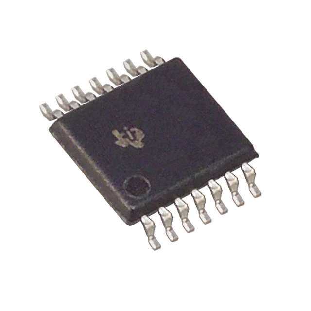
| 产品图片 |
|
| rohs | 符合RoHS无铅 / 符合限制有害物质指令(RoHS)规范要求 |
| 产品系列 | 放大器 IC,运算放大器 - 运放,Texas Instruments TLV272QDRQ1- |
| 数据手册 | |
| 产品型号 | TLV272QDRQ1 |
| 产品目录页面 | |
| 产品种类 | 运算放大器 - 运放 |
| 供应商器件封装 | 8-SOIC |
| 共模抑制比—最小值 | 58 dB |
| 关闭 | No Shutdown |
| 其它名称 | 296-17870-1 |
| 包装 | 剪切带 (CT) |
| 压摆率 | 2.1 V/µs |
| 双重电源电压 | +/- 3 V, +/- 5 V |
| 商标 | Texas Instruments |
| 增益带宽生成 | 3 MHz |
| 增益带宽积 | 3MHz |
| 安装类型 | 表面贴装 |
| 安装风格 | SMD/SMT |
| 封装 | Reel |
| 封装/外壳 | 8-SOIC(0.154",3.90mm 宽) |
| 封装/箱体 | SOIC-8 |
| 工作温度 | -40°C ~ 125°C |
| 工作电源电压 | 2.7 V to 16 V, +/- 1.35 V to +/- 8 V |
| 工厂包装数量 | 2500 |
| 技术 | CMOS |
| 放大器类型 | 通用 |
| 最大双重电源电压 | +/- 8 V |
| 最大工作温度 | + 125 C |
| 最小双重电源电压 | +/- 1.35 V |
| 最小工作温度 | - 40 C |
| 标准包装 | 1 |
| 电压-电源,单/双 (±) | 2.7 V ~ 16 V, ±1.35 V ~ 8 V |
| 电压-输入失调 | 500µV |
| 电流-电源 | 750µA |
| 电流-输入偏置 | 1pA |
| 电流-输出/通道 | 13mA |
| 电源电流 | 1.8 mA |
| 电路数 | 2 |
| 系列 | TLV272-Q1 |
| 设计资源 | http://www.digikey.com/product-highlights/cn/zh/texas-instruments-webench-design-center/3176 |
| 转换速度 | 2.5 V/us |
| 输入偏压电流—最大 | 60 pA |
| 输入参考电压噪声 | 39 nV |
| 输入补偿电压 | 5 mV |
| 输出电流 | 13 mA |
| 输出类型 | 满摆幅 |
| 通道数量 | 2 Channel |


- 商务部:美国ITC正式对集成电路等产品启动337调查
- 曝三星4nm工艺存在良率问题 高通将骁龙8 Gen1或转产台积电
- 太阳诱电将投资9.5亿元在常州建新厂生产MLCC 预计2023年完工
- 英特尔发布欧洲新工厂建设计划 深化IDM 2.0 战略
- 台积电先进制程称霸业界 有大客户加持明年业绩稳了
- 达到5530亿美元!SIA预计今年全球半导体销售额将创下新高
- 英特尔拟将自动驾驶子公司Mobileye上市 估值或超500亿美元
- 三星加码芯片和SET,合并消费电子和移动部门,撤换高东真等 CEO
- 三星电子宣布重大人事变动 还合并消费电子和移动部门
- 海关总署:前11个月进口集成电路产品价值2.52万亿元 增长14.8%


PDF Datasheet 数据手册内容提取
TLV271-Q1, TLV272-Q1, TLV274-Q1 µ FAMILY OF 550- A/Ch 3-MHz RAIL-TO-RAIL OUTPUT OPERATIONAL AMPLIFIERS SGLS275A − OCTOBER 2004 − REVISED JUNE 2008 (cid:1) Qualified for Automotive Applications Operational Amplifier (cid:1) Rail-To-Rail Output (cid:1) Wide Bandwidth...3 MHz + (cid:1) High Slew Rate...2 .4 V/µs − (cid:1) Supply Voltage Range...2.7 V to 16 V (cid:1) Supply Current...550 µA/Channel (cid:1) Input Noise Voltage...39 nV/√Hz (cid:1) Input Bias Current...1 pA (cid:1) Specified Temperature Range −40°C to 125°C...Automotive Grade (cid:1) Ultrasmall Packaging − 5-Pin SOT-23 (TLV271) (cid:1) Ideal Upgrade for TLC27x Family description The TLV27x takes the minimum operating supply voltage down to 2.7 V over the extended automotive temperature range while adding the rail-to-rail output swing feature. This makes it an ideal alternative to the TLC27x family for applications where rail-to-rail output swings are essential. The TLV27x also provides 3-MHz bandwidth from only 550 µA. Like the TLC27x, the TLV27x is fully specified for 5-V and ±5-V supplies. The maximum recommended supply voltage is 16 V, which allows the devices to be operated from a variety of rechargeable cells (±8 V supplies down to ±1.35 V). The CMOS inputs enable use in high-impedance sensor interfaces, with the lower voltage operation making an attractive alternative for the TLC27x in battery-powered applications. The 2.7-V operation makes it compatible with Li-Ion powered systems and the operating supply voltage range of many micropower microcontrollers available today including Texas Instruments MSP430. SELECTION OF SIGNAL AMPLIFIER PRODUCTS† RAIL- DEVICE VDD (V) (VµIVO) I(qµ/CAh) IIB (pA) (GMBHWz) (VS/µRs) SHUTDOWN TO- SINGLES/DUALS/QUADS RAIL TLV27x 2.7−16 500 550 1 3 2.4 — O S/D/Q TLC27x 3−16 1100 675 1 1.7 3.6 — — S/D/Q TLV237x 2.7−16 500 550 1 3 2.4 Yes I/O S/D/Q TLC227x 4−16 300 1100 1 2.2 3.6 — O D/Q TLV246x 2.7−6 150 550 1300 6.4 1.6 Yes I/O S/D/Q TLV247x 2.7−6 250 600 2 2.8 1.5 Yes I/O S/D/Q TLV244x 2.7−10 300 725 1 1.8 1.4 — O D/Q †Typical values measured at 5 V, 25°C Please be aware that an important notice concerning availability, standard warranty, and use in critical applications of TexasInstruments semiconductor products and disclaimers thereto appears at the end of this data sheet. PRODUCTION DATA information is current as of publication date. Copyright 2008 Texas Instruments Incorporated Products conform to specifications per the terms of Texas Instruments standard warranty. Production processing does not necessarily include testing of all parameters. POST OFFICE BOX 655303 • DALLAS, TEXAS 75265 1
TLV271-Q1, TLV272-Q1, TLV274-Q1 µ FAMILY OF 550- A/Ch 3-MHz RAIL-TO-RAIL OUTPUT OPERATIONAL AMPLIFIERS SGLS275A − OCTOBER 2004 − REVISED JUNE 2008 (cid:1) FAMILY PACKAGE TABLE (cid:2) NNUUMMBBEERR OOFF PACKAGE TYPES UUNNIIVVEERRSSAALL DDEEVVIICCEE CHANNELS SOIC SOT-23 TSSOP MSOP§ EVM BOARD TLV271 1 8 5 — — SSeeee tthhee EEVVMM TLV272 2 8 — — 8 SSeelleeccttiioonn GGuuiiddee (SLOU060) TLV274 4 14 — 14 — †For the most current package and ordering information, see the Package Option Addendum at the end of this document, or see the TI web site at http://www.ti.com. ‡Package drawings, thermal data, and symbolization are available at http://www.ti.com/packaging. §Product Preview TLV271 AVAILABLE OPTIONS PACKAGED DEVICES TTAA VVIOMM2255AA°°CCXX AATT SSMMAALLLL OOUUTTLLIINNEE SOT-23 (D) (DBV) SYMBOL −40°C to 125°C 5 mV TLV271QDRQ1 TLV271QDBVRQ1 271Q TLV272 AVAILABLE OPTIONS PACKAGED DEVICES TTAA VVIOMM2255AA°°CCXX AATT SSMMAALLLL OOUUTTLLIINNEE MSOP (D) (DGK) SYMBOL −40°C to 125°C 5 mV TLV272QDRQ1 TLV272QDGKRQ1† †Product Preview TLV274 AVAILABLE OPTIONS PACKAGED DEVICES TA VIOMAX AT 25°C SMALL OUTLINE TSSOP (D) (PW) −40°C to 125°C 5 mV TLV274QDRQ1 TLV274QPWRQ1 2 POST OFFICE BOX 655303 • DALLAS, TEXAS 75265
TLV271-Q1, TLV272-Q1, TLV274-Q1 µ FAMILY OF 550- A/Ch 3-MHz RAIL-TO-RAIL OUTPUT OPERATIONAL AMPLIFIERS SGLS275A − OCTOBER 2004 − REVISED JUNE 2008 TLV27x PACKAGE PINOUTS(1) TLV271 TLV271 DBV PACKAGE D PACKAGE (TOP VIEW) (TOP VIEW) OUT 1 5 VDD NC 1 8 NC IN− 2 7 VDD GND 2 IN+ 3 6 OUT GND 4 5 NC IN+ 3 4 IN− TLV272 TLV274 D OR DGK PACKAGE D OR PW PACKAGE (TOP VIEW) (TOP VIEW) 1OUT 1 8 VDD 1OUT 1 14 4OUT 1IN− 2 7 2OUT 1IN− 2 13 4IN− 1IN+ 3 6 2IN− 1IN+ 3 12 4IN+ GND 4 5 2IN+ VDD 4 11 GND 2IN+ 5 10 3IN+ 2IN− 6 9 3IN− 2OUT 7 8 3OUT NC − No internal connection (1) SOT−23 may or may not be indicated TYPICAL PIN 1 INDICATORS Pin 1 Printed or Pin 1 Pin 1 Pin 1 Molded Dot Stripe Bevel Edges Molded ”U” Shape POST OFFICE BOX 655303 • DALLAS, TEXAS 75265 3
TLV271-Q1, TLV272-Q1, TLV274-Q1 µ FAMILY OF 550- A/Ch 3-MHz RAIL-TO-RAIL OUTPUT OPERATIONAL AMPLIFIERS SGLS275A − OCTOBER 2004 − REVISED JUNE 2008 absolute maximum ratings over operating free-air temperature range (unless otherwise noted)† Supply voltage, V (see Note 1) . . . . . . . . . . . . . . . . . . . . . . . . . . . . . . . . . . . . . . . . . . . . . . . . . . . . . . . . . . 16.5 V DD Differential input voltage, V . . . . . . . . . . . . . . . . . . . . . . . . . . . . . . . . . . . . . . . . . . . . . . . . . . . . . . . . . . . . . . . ±V ID DD Input voltage range, VI (see Note 1) . . . . . . . . . . . . . . . . . . . . . . . . . . . . . . . . . . . . . . . . . . . −0.2 V to VDD + 0.2 V Input current range, I . . . . . . . . . . . . . . . . . . . . . . . . . . . . . . . . . . . . . . . . . . . . . . . . . . . . . . . . . . . . . . . . . . . . ±10 mA I Output current range, I . . . . . . . . . . . . . . . . . . . . . . . . . . . . . . . . . . . . . . . . . . . . . . . . . . . . . . . . . . . . . . . . ±100 mA O Continuous total power dissipation . . . . . . . . . . . . . . . . . . . . . . . . . . . . . . . . . . . . . See Dissipation Rating Table Operating free-air temperature range, T . . . . . . . . . . . . . . . . . . . . . . . . . . . . . . . . . . . . . . . . . −40°C to 125°C A Maximum junction temperature, T . . . . . . . . . . . . . . . . . . . . . . . . . . . . . . . . . . . . . . . . . . . . . . . . . . . . . . . . . 150°C J Storage temperature range, T . . . . . . . . . . . . . . . . . . . . . . . . . . . . . . . . . . . . . . . . . . . . . . . . . . . −65°C to 150°C stg Lead temperature 1,6 mm (1/16 inch) from case for 10 seconds . . . . . . . . . . . . . . . . . . . . . . . . . . . . . . . 260°C †Stresses beyond those listed under “absolute maximum ratings” may cause permanent damage to the device. These are stress ratings only, and functional operation of the device at these or any other conditions beyond those indicated under “recommended operating conditions” is not implied. Exposure to absolute-maximum-rated conditions for extended periods may affect device reliability. NOTE 1: All voltage values, except differential voltages, are with respect to GND. DISSIPATION RATING TABLE PACKAGE θJC θJA TA ≤ 25°C TA = 25°C (°C/W) (°C/W) POWER RATING POWER RATING D (8) 38.3 176 710 mW 396 mW D (14) 26.9 122.3 1022 mW 531 mW DBV (5) 55 324.1 385 mW 201 mW DGK (8) 54.23 259.96 481 mW 250 mW PW (14) 29.3 173.6 720 mW 374 mW recommended operating conditions MIN MAX UNIT Single supply 2.7 16 SSuuppppllyy vvoollttaaggee, VVDD Split supply ±1.35 ±8 VV Common-mode input voltage range, VICR 0 VDD−1.35 V Operating free-air temperature, TA Q-suffix −40 125 °C 4 POST OFFICE BOX 655303 • DALLAS, TEXAS 75265
TLV271-Q1, TLV272-Q1, TLV274-Q1 µ FAMILY OF 550- A/Ch 3-MHz RAIL-TO-RAIL OUTPUT OPERATIONAL AMPLIFIERS SGLS275A − OCTOBER 2004 − REVISED JUNE 2008 electrical characteristics at specified free-air temperature, V = 2.7 V, 5 V, and 15 V (unless DD otherwise noted) dc performance PARAMETER TEST CONDITIONS TA† MIN TYP MAX UNIT 25°C 0.5 5 VVIO IInnppuutt ooffffsseett vvoollttaaggee VVIC = VVDD//22, VVO = VVDD//22, Full range 7 mmVV αVIO Offset voltage drift RRLL == 1100 kkΩΩ, RRSS == 5500 ΩΩ 25°C 2 µV/°C VVRIISCC === 5000 ttooΩ VVDDDD−11..3355VV,, VVDD = 22.77 VV Fu2ll 5r°aCnge 5534 70 CCMMRRRR CCoommmmoonn-mmooddee rreejjeeccttiioonn rraattiioo VVRIISCC === 5000 ttooΩ VVDDDD−11..3355VV,, VVDD = 55 VV Fu2ll 5r°aCnge 5587 80 ddBB VVRIISCC === 5000 ttooΩ VVDDDD−11..3355VV,, VVDD = 1155 VV Fu2ll 5r°aCnge 6676 85 25°C 95 106 VVDD = 22.77 VV Full range 76 AAVD LLaaamrrpggleeif-issciiaggtnnioaanll ddiiffffeerreennttiiaall vvoollttaaggee VVROOL ((=PP PP1))0 == k VVΩDDDD//22,, VVDD = 55 VV Fu2ll 5r°aCnge 8802 110 ddBB 25°C 77 115 VVDD = 1155 VV Full range 79 †Full range is −40°C to 125°C. If not specified, full range is −40°C to 125°C. input characteristics PARAMETER TEST CONDITIONS TA MIN TYP MAX UNIT 25°C 1 60 IIIO IInnppuutt ooffffsseett ccuurrrreenntt VVDDDD == 1155 VV,, VVIICC == VVDDDD//22,, 125°C 1000 ppAA VOO = VDDDD/2,, RSS = 50 Ω 25°C 1 60 IIIB IInnppuutt bbiiaass ccuurrrreenntt 125°C 1000 ppAA ri(d) Differential input resistance 25°C 1000 GΩ CIC Common-mode input capacitance f = 21 kHz 25°C 8 pF POST OFFICE BOX 655303 • DALLAS, TEXAS 75265 5
TLV271-Q1, TLV272-Q1, TLV274-Q1 µ FAMILY OF 550- A/Ch 3-MHz RAIL-TO-RAIL OUTPUT OPERATIONAL AMPLIFIERS SGLS275A − OCTOBER 2004 − REVISED JUNE 2008 electrical characteristics at specified free-air temperature, V = 2.7 V, 5 V, and 15 V (unless DD otherwise noted) output characteristics PARAMETER TEST CONDITIONS TA† MIN TYP MAX UNIT 25°C 2.55 2.58 VVDD = 22.77 VV Full range 2.48 25°C 4.9 4.93 VVIC = VVDD//22, IIOH = −11 mmAA VVDD = 55 VV Full range 4.85 25°C 14.92 14.96 VVDD = 1155 VV Full range 14.9 VVOH HHiigghh-lleevveell oouuttppuutt vvoollttaaggee 25°C 1.88 2.1 VV VVDD = 22.77 VV Full range 1.42 25°C 4.58 4.68 VVIC = VVDD//22, IIOH = −55 mmAA VVDD = 55 VV Full range 4.44 25°C 14.7 14.8 VVDD = 1155 VV Full range 14.6 25°C 0.1 0.15 VVDD = 22.77 VV Full range 0.22 25°C 0.05 0.1 VVIC = VVDD//22, IIOL = 11 mmAA VVDD = 55 VV Full range 0.15 25°C 0.05 0.08 VVDD = 1155 VV Full range 0.1 VVOL LLooww-lleevveell oouuttppuutt vvoollttaaggee 25°C 0.5 0.7 VV VVDD = 22.77 VV Full range 1.15 25°C 0.28 0.4 VVIC = VVDD//22, IIOL = 55 mmAA VVDD = 55 VV Full range 0.54 25°C 0.19 0.3 VVDD = 1155 VV Full range 0.35 Positive rail 25°C 4 VVO == 00.55 VV ffrroomm rraaiill, VVDD == 22.77 VV Negative rail 25°C 5 Positive rail 25°C 7 IIO OOuuttppuutt ccuurrrreenntt VVO == 00.55 VV ffrroomm rraaiill, VVDD == 55 VV Negative rail 25°C 8 mmAA Positive rail 25°C 13 VVO == 00.55 VV ffrroomm rraaiill, VVDD == 1155 VV Negative rail 25°C 12 †Full range is −40°C to 125°C. If not specified, full range is −40°C to 125°C. ‡Depending on package dissipation rating 6 POST OFFICE BOX 655303 • DALLAS, TEXAS 75265
TLV271-Q1, TLV272-Q1, TLV274-Q1 µ FAMILY OF 550- A/Ch 3-MHz RAIL-TO-RAIL OUTPUT OPERATIONAL AMPLIFIERS SGLS275A − OCTOBER 2004 − REVISED JUNE 2008 electrical characteristics at specified free-air temperature, V = 2.7 V, 5 V, and 15 V (unless DD otherwise noted) (continued) power supply PARAMETER TEST CONDITIONS TA† MIN TYP MAX UNIT VDD = 2.7 V 25°C 470 560 IIDD SSuuppppllyy ccuurrrreenntt ((ppeerr cchhaannnneell)) VVO == VVDD//22 VDD = 5 V 2255°°CC 575500 696000 µµAA VVDD == 1155 VV Full range 1200 PPSSRRRR SS(∆uuVppDppDllyy /vv∆ooVllttIaaOgg)ee rreejjeeccttiioonn rraattiioo VVNDDoDD lo ==a d 22..77 VV ttoo 1155 VV,, VVIICC == VVDDDD//22,, Fu2ll 5r°aCnge 7605 80 ddBB †Full range is −40°C to 125°C. If not specified, full range is −40°C to 125°C. dynamic performance PARAMETER TEST CONDITIONS TA† MIN TYP MAX UNIT VDD = 2.7 V 25°C 2.4 UUGGBBWW UUnniittyy ggaaiinn bbaannddwwiiddtthh RRL = 22 kkΩΩ, CCL = 1100 ppFF VDD = 5 V to 15 V 25°C 3 MMHHzz 25°C 1.4 2.1 VVDD = 22.77 VV Full range 1 VV//µss SSRR SSlleeww rraattee aatt uunniittyy ggaaiinn VVCOOL ((=PP PP5))0 == p VVFDD, DDR//L22 ,,= 10 kΩ, VVDD = 55 VV Fu2ll 5r°aCnge 11..42 2.4 VV//µss 25°C 1.9 2.1 VVDD = 1155 VV Full range 1.4 VV//µss φm Phase margin RL = 2 kΩ CL = 10 pF 25°C 65 ° Gain margin RL = 2 kΩ CL = 10 pF 25°C 18 dB VDD = 2.7 V, V(STEP)PP = 1 V, AV = −1, 0.1% 2.9 CL = 10 pF, RL = 2 kΩ tts SSeettttlliinngg ttiimmee VDD = 5 V, 15 V, 2255°°CC µss V(STEP)PP = 1 V, AV = −1, 0.1% 2 CL = 47 pF, RL = 2 kΩ †Full range is −40°C to 125°C. If not specified, full range is −40°C to 125°C. noise/distortion performance PARAMETER TEST CONDITIONS TA MIN TYP MAX UNIT VVDDDD == 22..77 VV,, AV = 1 0.02% VVOO((PPPP)) = VVDDDD//22 VV,, AV = 10 2255°CC 0.05% RL = 2 kΩ, f = 10 kHz AV = 100 0.18% TTHHDD + NN TToottaall hhaarrmmoonniicc ddiissttoorrttiioonn pplluuss nnooiissee VVDDDD == 55 VV,, ±±55 VV,, AV = 1 0.02% VVOO((PPPP)) = VVDDDD//22 VV,, AV = 10 2255°CC 0.09% RL = 2 kΩ, f = 10K AV = 100 0.5% f = 1 kHz 39 VVn EEqquuiivvaalleenntt iinnppuutt nnooiissee vvoollttaaggee f = 10 kHz 2255°°CC 35 nnVV//√√HHzz In Equivalent input noise current f = 1 kHz 25°C 0.6 fA/√Hz POST OFFICE BOX 655303 • DALLAS, TEXAS 75265 7
TLV271-Q1, TLV272-Q1, TLV274-Q1 µ FAMILY OF 550- A/Ch 3-MHz RAIL-TO-RAIL OUTPUT OPERATIONAL AMPLIFIERS SGLS275A − OCTOBER 2004 − REVISED JUNE 2008 TYPICAL CHARACTERISTICS Table of Graphs FIGURE CMRR Common-mode rejection ratio vs Frequency 1 Input bias and offset current vs Free-air temperature 2 VOL Low-level output voltage vs Low-level output current 3, 5, 7 VOH High-level output voltage vs High-level output current 4, 6, 8 VO(PP) Peak-to-peak output voltage vs Frequency 9 IDD Supply current vs Supply voltage 10 PSRR Power supply rejection ratio vs Frequency 11 AVD Differential voltage gain & phase vs Frequency 12 Gain-bandwidth product vs Free-air temperature 13 vs Supply voltage 14 SSRR SSlleeww rraattee vs Free-air temperature 15 φm Phase margin vs Capacitive load 16 Vn Equivalent input noise voltage vs Frequency 17 Voltage-follower large-signal pulse response 18, 19 Voltage-follower small-signal pulse response 20 Inverting large-signal response 21, 22 Inverting small-signal response 23 Crosstalk vs Frequency 24 8 POST OFFICE BOX 655303 • DALLAS, TEXAS 75265
TLV271-Q1, TLV272-Q1, TLV274-Q1 µ FAMILY OF 550- A/Ch 3-MHz RAIL-TO-RAIL OUTPUT OPERATIONAL AMPLIFIERS SGLS275A − OCTOBER 2004 − REVISED JUNE 2008 TYPICAL CHARACTERISTICS COMMON-MODE REJECTION RATIO INPUT BIAS AND OFFSET CURRENT LOW-LEVEL OUTPUT VOLTAGE vs vs vs FREQUENCY FREE-AIR TEMPERATURE LOW-LEVEL OUTPUT CURRENT ction Ratio − dB 11028000 VDD = 5 V, 10 V set Current − pA 223050000 VVDICD = = V 2D.7D /V2, 5 V and 10 V ut Voltage − V 222...048000 TVA D=D 1 =2 52 .°7C V mmon-Mode Reje 4600 VDD = 2.7 V nput Bias and Off 11055000 − Low-Level Outp 011...826000 TAT A= =2 57 0°C °C CMRR − Co 20010 100 1 k 10 k 100 k 1 M − IIIIBIO −500−40−25−105 20 35 50 65 80 95 110125 VOL 00..04000 2 4 6TA8 = 4100 °C12 14TA1 6= 01 8°C20 22 24 f − Frequency − Hz TA − Free-Air Temperature − °C IOL − Low-Level Output Current − mA Figure 1 Figure 2 Figure 3 HIGH-LEVEL OUTPUT VOLTAGE LOW-LEVEL OUTPUT VOLTAGE HIGH-LEVEL OUTPUT VOLTAGE vs vs vs HIGH-LEVEL OUTPUT CURRENT LOW-LEVEL OUTPUT CURRENT HIGH-LEVEL OUTPUT CURRENT 2.80 5.00 5.00 V− High-Level Output Voltage − VOH 001122......482604000000 TAT A= =T1A T27 A5=0 °° =2CC 50°°CC VTDAD = =− 420.7°C V V− Low-Level Output Voltage − VOL 011223344.........505050505000000000 TVATD AD= =7= 0 15 2° VC5 °CTA = −40 °CTAT =A 0= °2C5 °C V− High-Level Output Voltage − VOH 011223344.........505050505000000000 TA T=A 2T =5A ° 7C=0 1°C25°CTA = −40°CTVAC =C 0 =° C5 V 0.00 0.00 0.00 0 1 2 3 4 5 6 7 8 9 10 11 12 0 5 10152025303540455055606570 0 5 10 15 20 25 30 35 40 45 IOH − High-Level Output Current − mA IOL − Low-Level Output Current − mA IOH − High-Level Output Current − mA Figure 4 Figure 5 Figure 6 LOW-LEVEL OUTPUT VOLTAGE HIGH-LEVEL OUTPUT VOLTAGE PEAK-TO-PEAK OUTPUT VOLTAGE vs vs vs LOW-LEVEL OUTPUT CURRENT HIGH-LEVEL OUTPUT CURRENT FREQUENCY 10 10 V 11 − Low-Level Output Voltage − VOL 2468 TVADT =DATT− =A=A4 001==°°072CC 05V°T°CCA =125°C − High-Level Output Voltage − VH 2468 TTATA A= = =7 0 02°°5CC°C VDTDA = = 1−04 V0°C − Peak-to-Peak Output Voltage − P) 1023456789 ARCTTAVHLL D====V VV2−21=DD51D 0 Dk5°D0 DΩ pC%= =F= 2 51.7 0V VV V VO TA = 125°C O(P 1 0 0 V 0 0 20 40 60 80 100 120 0 20 40 60 80 100 120 10 100 1 k 10 k 100 k 1 M 10 M IOL − Low-Level Output Current − mA IOH − High-Level Output Current − mA f − Frequency − Hz Figure 7 Figure 8 Figure 9 POST OFFICE BOX 655303 • DALLAS, TEXAS 75265 9
TLV271-Q1, TLV272-Q1, TLV274-Q1 µ FAMILY OF 550- A/Ch 3-MHz RAIL-TO-RAIL OUTPUT OPERATIONAL AMPLIFIERS SGLS275A − OCTOBER 2004 − REVISED JUNE 2008 TYPICAL CHARACTERISTICS SUPPLY CURRENT POWER SUPPLY REJECTION RATIO vs vs SUPPLY VOLTAGE FREQUENCY 1.0 B 120 0.9 AV = 1 − d TA = 25°C pply Current − mA/ch 00000.....45678 VIC =TA V =D D7 0/ °2C TTAA = = 1 2255°°CC Supply Rejection Ratio 1068000 VDD = 2V.7D VD = 5 V, 10 V Su− 0.3 TA = 0°C wer 40 DD 0.2 TA = −40°C − Po 20 I 0.1 RR S 0.0 P 0 0 1 2 3 4 5 6 7 8 9 101112131415 10 100 1 k 10 k 100 k 1 M VDD − Supply Voltage − V f − Frequency − Hz Figure 10 Figure 11 DIFFERENTIAL VOLTAGE GAIN AND PHASE GAIN BANDWIDTH PRODUCT vs vs FREQUENCY FREE-AIR TEMPERATURE 120 180 4.0 B 100 135 MHz 3.5 n − d 80 Phase 90 uct − 3.0 VDD = 10 V ntial Voltage Gai 246000 Gain −04545°Phase − Bandwidth Prod 122...505 VDD = 5 V VDD = 2.7 V − DiffereVD −200 VRCTADLL===D221=5 05k° ΩpCVF −−19305 BWP −Gain 01..50 A G −40 −180 0.0 10 100 1 k 10 k 100 k 1 M 10 M −40−25−10 5 20 35 50 65 80 95 110125 f − Frequency − Hz TA − Free-Air Temperature − °C Figure 12 Figure 13 SLEW RATE SLEW RATE PHASE MARGIN vs vs vs SUPPLY VOLTAGE FREE-AIR TEMPERATURE CAPACITIVE LOAD 3.0 3.5 100 2.5 SR− 3.0 90 VRDL=D 2= k5Ω V µsSR − Slew Rate − V/ 112...050 SR+ ARVL == 110 kΩ µSR − Slew Rate − V/s 1122....0505 SSRR−+ VAVD D= =1 5 V °Phase Margin − 345678000000 Rnull TA=AV 0 == 2O5p°ReCnnu Lll o=o 1p00 0.5 CL = 50 pF RL = 10 kΩ 20 Rnull = 50 TA = 25°C 0.5 CVIL = = 35 0V pF 10 0.0 0.0 0 2.5 4.5 6.5 8.5 10.5 12.5 14.5 −40−25−10 5 20 35 50 65 80 95110 125 10 100 1000 VCC − Supply Voltage −V TA − Free-Air Temperature − °C CL − Capacitive Load − pF Figure 14 Figure 15 Figure 16 10 POST OFFICE BOX 655303 • DALLAS, TEXAS 75265
TLV271-Q1, TLV272-Q1, TLV274-Q1 µ FAMILY OF 550- A/Ch 3-MHz RAIL-TO-RAIL OUTPUT OPERATIONAL AMPLIFIERS SGLS275A − OCTOBER 2004 − REVISED JUNE 2008 TYPICAL CHARACTERISTICS EQUIVALENT INPUT NOISE VOLTAGE vs VOLTAGE-FOLLOWER LARGE-SIGNAL FREQUENCY PULSE RESPONSE nV/HzNoise Voltage − 1056789000000 VTAD D= =2 52°.C7, 5, 10 V V− Input Voltage − VI 01234 VI CVVARTAVDILL = D==== 3 =2121 5V 05k° PΩpCVPF age − V put 40 3 Volt Equivalent In 123000 VO 012 V− Output O − 0 n 10 100 1 k 10 k 100 k 0 2 4 6 8 10 12 14 16 18 V f − Frequency − Hz t − Time − µs Figure 17 Figure 18 VOLTAGE-FOLLOWER LARGE-SIGNAL VOLTAGE-FOLLOWER SMALL-SIGNAL PULSE RESPONSE PULSE RESPONSE 8 V V− Input Voltage − VI 0246 VVIO VARCVTAVDILL = D==== 6 =2121 5V 01k° 0PΩpC PFV 6420 − Output Voltage − VO V− Input Voltage − mI0000....00010482 VVOI VAR VTCAVDIL L = D== == 1 =21 210 5 500k° Ω CVpmFVPP 0000....00010482 Output Voltage − mV V − O 0 2 4 6 8 10 12 14 16 18 0.0 0.20.40.60.8 1.0 1.21.41.61.8 V t − Time − µs t − Time − µs Figure 19 Figure 20 INVERTING LARGE-SIGNAL RESPONSE INVERTING LARGE-SIGNAL RESPONSE V− Input Voltage − VI 43210 VARCVTAVDILL = D==== 3 =2121 5V 05k° PΩpCVPF VI 23 ut Voltage − V − Input Voltage − VVI 02468 VARCTAVDLL D==== 2V21=5 0I k 1° =ΩpC0 F− V1 VI VO 64 Voltage − V VO 01 V− OutpO 20 − Output O 0 22 4 6 8 10 12 14 16 0 2 4 6 8 10 12 14 16 V t − Time − µs t − Time − µs Figure 21 Figure 22 POST OFFICE BOX 655303 • DALLAS, TEXAS 75265 11
TLV271-Q1, TLV272-Q1, TLV274-Q1 µ FAMILY OF 550- A/Ch 3-MHz RAIL-TO-RAIL OUTPUT OPERATIONAL AMPLIFIERS SGLS275A − OCTOBER 2004 − REVISED JUNE 2008 TYPICAL CHARACTERISTICS CROSSTALK vs INVERTING SMALL-SIGNAL RESPONSE FREQUENCY 0 V − VDD = 2.7, 5, & 15 V − Input Voltage VI000...001050 RCVVATAVDILL = D==== 1 2V21=05 0I 0k 5° =Ω pC m VF−V1pp VVOI 00..0150 Voltage − V Crosstalk − dB −−−−−10864200000 VARTAVIL = === 1 212 5V k°DΩCD/2 Crosstalk ut 0.00 utp −120 O − O −140 0.0 0.5 1.01.52.02.5 3.0 3.54.0 4.5 V 10 100 1 k 10 k 100 k t − Time − µs f − Frequency − Hz Figure 23 Figure 24 APPLICATION INFORMATION driving a capacitive load When the amplifier is configured in this manner, capacitive loading directly on the output decreases the device’s phase margin leading to high frequency ringing or oscillations. Therefore, for capacitive loads of greater than 10 pF, it is recommended that a resistor be placed in series (R ) with the output of the amplifier, as shown NULL in Figure 25. A minimum value of 20 Ω should work well for most applications. RF RG Input − RNULL Output + CLOAD VDD/2 Figure 25. Driving a Capacitive Load 12 POST OFFICE BOX 655303 • DALLAS, TEXAS 75265
TLV271-Q1, TLV272-Q1, TLV274-Q1 µ FAMILY OF 550- A/Ch 3-MHz RAIL-TO-RAIL OUTPUT OPERATIONAL AMPLIFIERS SGLS275A − OCTOBER 2004 − REVISED JUNE 2008 APPLICATION INFORMATION offset voltage The output offset voltage (V ) is the sum of the input offset voltage (V ) and both input bias currents (I ) times OO IO IB the corresponding gains. The following schematic and formula can be used to calculate the output offset voltage: RF IIB− RG (cid:2) (cid:4) (cid:2) (cid:4) (cid:2) (cid:4) (cid:2) (cid:4) + − R R VI + VO VOO(cid:1)VIO 1(cid:3) RF (cid:5)IIB(cid:3)RS 1(cid:3) RF (cid:5)IIB–RF G G RS IIB+ Figure 26. Output Offset Voltage Model general configurations When receiving low-level signals, limiting the bandwidth of the incoming signals into the system is often required. The simplest way to accomplish this is to place an RC filter at the noninverting terminal of the amplifier (see Figure 27). RG RF (cid:2) (cid:4) V R (cid:2) (cid:4) O (cid:1) 1(cid:3) F 1 V R 1(cid:3)sR1C1 VDD/2 I G − VI + VO f–3dB (cid:1) 2(cid:1)R11C1 R1 C1 Figure 27. Single-Pole Low-Pass Filter If even more attenuation is needed, a multiple pole filter is required. The Sallen-Key filter can be used for this task. For the best results, the amplifier should have a bandwidth that is 8 to 10 times the filter frequency bandwidth. Failure to do this can result in phase shift of the amplifier. C1 R1 = R2 = R C1 = C2 = C Q = Peaking Factor (Butterworth Q = 0.707) VI + R1 R2 _ f (cid:1) 1 –3dB 2(cid:1)RC C2 RF RG = (2 −RF1 ) RG Q VDD/2 Figure 28. 2-Pole Low-Pass Sallen-Key Filter POST OFFICE BOX 655303 • DALLAS, TEXAS 75265 13
TLV271-Q1, TLV272-Q1, TLV274-Q1 µ FAMILY OF 550- A/Ch 3-MHz RAIL-TO-RAIL OUTPUT OPERATIONAL AMPLIFIERS SGLS275A − OCTOBER 2004 − REVISED JUNE 2008 APPLICATION INFORMATION circuit layout considerations To achieve the levels of high performance of the TLV27x, follow proper printed-circuit board design techniques. A general set of guidelines is given in the following. (cid:1) Ground planes—It is highly recommended that a ground plane be used on the board to provide all components with a low inductive ground connection. However, in the areas of the amplifier inputs and output, the ground plane can be removed to minimize the stray capacitance. (cid:1) Proper power supply decoupling—Use a 6.8-µF tantalum capacitor in parallel with a 0.1-µF ceramic capacitor on each supply terminal. It may be possible to share the tantalum among several amplifiers depending on the application, but a 0.1-µF ceramic capacitor should always be used on the supply terminal of every amplifier. In addition, the 0.1-µF capacitor should be placed as close as possible to the supply terminal. As this distance increases, the inductance in the connecting trace makes the capacitor less effective. The designer should strive for distances of less than 0.1 inches between the device power terminals and the ceramic capacitors. (cid:1) Sockets—Sockets can be used but are not recommended. The additional lead inductance in the socket pins will often lead to stability problems. Surface-mount packages soldered directly to the printed-circuit board is the best implementation. (cid:1) Short trace runs/compact part placements—Optimum high performance is achieved when stray series inductance has been minimized. To realize this, the circuit layout should be made as compact as possible, thereby minimizing the length of all trace runs. Particular attention should be paid to the inverting input of the amplifier. Its length should be kept as short as possible. This helps to minimize stray capacitance at the input of the amplifier. (cid:1) Surface-mount passive components—Using surface-mount passive components is recommended for high performance amplifier circuits for several reasons. First, because of the extremely low lead inductance of surface-mount components, the problem with stray series inductance is greatly reduced. Second, the small size of surface-mount components naturally leads to a more compact layout thereby minimizing both stray inductance and capacitance. If leaded components are used, it is recommended that the lead lengths be kept as short as possible. 14 POST OFFICE BOX 655303 • DALLAS, TEXAS 75265
TLV271-Q1, TLV272-Q1, TLV274-Q1 µ FAMILY OF 550- A/Ch 3-MHz RAIL-TO-RAIL OUTPUT OPERATIONAL AMPLIFIERS SGLS275A − OCTOBER 2004 − REVISED JUNE 2008 APPLICATION INFORMATION general power dissipation considerations For a given θ , the maximum power dissipation is shown in Figure 29 and is calculated by the following formula: JA (cid:2) (cid:4) T –T P (cid:1) MAX A D (cid:1) JA Where: P = Maximum power dissipation of TLV27x IC (watts) D T = Absolute maximum junction temperature (150°C) MAX T = Free-ambient air temperature (°C) A θJA = θJC + θCA θ = Thermal coefficient from junction to case JC θ = Thermal coefficient from case to ambient air (°C/W) CA MAXIMUM POWER DISSIPATION vs FREE-AIR TEMPERATURE 2 PDIP Package TJ = 150°C 1.75 Low-K Test PCB θJA = 104°C/W W n − 1.5 MSOP Package o pati 1.25 SOIC Package LθJoAw =-K 2 6T0e°sCt /PWCB si Low-K Test PCB Dis θJA = 176°C/W r 1 e w o m P 0.75 u m xi 0.5 a M 0.25 SOT-23 Package Low-K Test PCB 0 θJA = 324°C/W −55−40−25 −10 5 20 35 50 65 80 95 110 125 TA − Free-Air Temperature − °C NOTE A: Results are with no air flow and using JEDEC Standard Low-K test PCB. Figure 29. Maximum Power Dissipation vs Free-Air Temperature POST OFFICE BOX 655303 • DALLAS, TEXAS 75265 15
TLV271-Q1, TLV272-Q1, TLV274-Q1 µ FAMILY OF 550- A/Ch 3-MHz RAIL-TO-RAIL OUTPUT OPERATIONAL AMPLIFIERS SGLS275A − OCTOBER 2004 − REVISED JUNE 2008 APPLICATION INFORMATION macromodel information Macromodel information provided was derived using Microsim Parts Release 9.1, the model generation software used with Microsim PSpice. The Boyle macromodel (see Note 2) and subcircuit in Figure 30 are generated using TLV27x typical electrical and operating characteristics at T = 25°C. Using this information, A output simulations of the following key parameters can be generated to a tolerance of 20% (in most cases): (cid:1) (cid:1) Maximum positive output voltage swing Unity-gain frequency (cid:1) (cid:1) Maximum negative output voltage swing Common-mode rejection ratio (cid:1) (cid:1) Slew rate Phase margin (cid:1) (cid:1) Quiescent power dissipation DC output resistance (cid:1) (cid:1) Input bias current AC output resistance (cid:1) (cid:1) Open-loop voltage amplification Short-circuit output current limit NOTE 2: G. R. Boyle, B. M. Cohn, D. O. Pederson, and J. E. Solomon, “Macromodeling of Integrated Circuit Operational Amplifiers,” IEEE Journal of Solid-State Circuits, SC-9, 353 (1974). 3 99 VDD + rp rd1 rd2 rss css egnd fb ro2 c1 − 7 11 12 + c2 1 vlim IN+ + 9 r2 6 − vc D D + 8 − 2 vb ga G G IN− 53 − gcm ioff ro1 S S OUT dp dlp dln 5 10 91 90 92 iss dc + + − vlp hlim vln GND − − + 4 − ve + 54 de *DEVICE=amp_tlv27x_highVdd,OP AMP,NJF,INT ga 6 0 11 12 16.272E−6 * amp_tlv_27x_highVdd operational amplifier ”macromodel” gcm 0 6 10 99 6.8698E−9 * subcircuit updated using Model Editor release 9.1 on 05/15/00 iss 10 4 dc 1.3371E−6 * at 14:40 Model Editor is an OrCAD product. hlim 90 0 vlim 1K * j1 11 2 10 jx1 * connections: non-inverting input J2 12 1 10 jx2 * | inverting input r2 6 9 100.00E3 * | | positive power supply rd1 3 11 61.456E3 * | | | negative power supply rd2 3 12 61.456E3 * | | | | output ro1 8 5 10 * | | | | | ro2 7 99 10 .subckt amp_tlv27x_highVdd 1 2 3 4 5 rp 3 4 150.51E3 * rss 10 99 149.58E6 c1 11 12 457.48E−15 vb 9 0 dc 0 c2 6 7 5.0000E−12 vc 3 53 dc .78905 css 10 99 1.1431E−12 ve 54 4 dc .78905 dc 5 53 dy vlim 7 8 dc 0 de 54 5 dy vlp 91 0 dc 14.200 dlp 90 91 dx vln 0 92 dc 14.200 dln 92 90 dx .model dx D(Is=800.00E−18) dp 4 3 dx .model dy D(Is=800.00E−18 Rs=1m Cjo=10p) egnd 99 0 poly(2) (3,0) (4,0) 0 .5 .5 .model jx1 NJF(Is=500.00E−15 Beta=198.03E−6 Vto=−1) fb 7 99 poly(5) vb vc ve vlp vln 0 .model jx2 NJF(Is=500.00E−15 Beta=198.03E−6 Vto=−1) 176.02E6 −1E3 1E3 180E6 .ends −180E6 Figure 30. Boyle Macromodel and Subcircuit PSpice and Parts are trademarks of MicroSim Corporation. 16 POST OFFICE BOX 655303 • DALLAS, TEXAS 75265
PACKAGE OPTION ADDENDUM www.ti.com 6-Feb-2020 PACKAGING INFORMATION Orderable Device Status Package Type Package Pins Package Eco Plan Lead/Ball Finish MSL Peak Temp Op Temp (°C) Device Marking Samples (1) Drawing Qty (2) (6) (3) (4/5) TLV271QDBVRQ1 ACTIVE SOT-23 DBV 5 3000 Green (RoHS NIPDAU Level-1-260C-UNLIM -40 to 125 271Q & no Sb/Br) TLV271QDRG4Q1 ACTIVE SOIC D 8 2500 Green (RoHS NIPDAU Level-1-260C-UNLIM -40 to 125 T271Q1 & no Sb/Br) TLV271QDRQ1 ACTIVE SOIC D 8 2500 Green (RoHS NIPDAU Level-1-260C-UNLIM -40 to 125 T271Q1 & no Sb/Br) TLV272QDRG4Q1 ACTIVE SOIC D 8 2500 Green (RoHS NIPDAU Level-1-260C-UNLIM -40 to 125 T272Q1 & no Sb/Br) TLV272QDRQ1 ACTIVE SOIC D 8 2500 Green (RoHS NIPDAU Level-1-260C-UNLIM -40 to 125 T272Q1 & no Sb/Br) TLV274QDRG4Q1 ACTIVE SOIC D 14 2500 Green (RoHS NIPDAU Level-1-260C-UNLIM -40 to 125 TLV274Q1 & no Sb/Br) TLV274QDRQ1 ACTIVE SOIC D 14 2500 Green (RoHS NIPDAU Level-1-260C-UNLIM -40 to 125 TLV274Q1 & no Sb/Br) TLV274QPWRG4Q1 ACTIVE TSSOP PW 14 2000 Green (RoHS NIPDAU Level-1-260C-UNLIM -40 to 125 TLV274Q & no Sb/Br) (1) The marketing status values are defined as follows: ACTIVE: Product device recommended for new designs. LIFEBUY: TI has announced that the device will be discontinued, and a lifetime-buy period is in effect. NRND: Not recommended for new designs. Device is in production to support existing customers, but TI does not recommend using this part in a new design. PREVIEW: Device has been announced but is not in production. Samples may or may not be available. OBSOLETE: TI has discontinued the production of the device. (2) RoHS: TI defines "RoHS" to mean semiconductor products that are compliant with the current EU RoHS requirements for all 10 RoHS substances, including the requirement that RoHS substance do not exceed 0.1% by weight in homogeneous materials. Where designed to be soldered at high temperatures, "RoHS" products are suitable for use in specified lead-free processes. TI may reference these types of products as "Pb-Free". RoHS Exempt: TI defines "RoHS Exempt" to mean products that contain lead but are compliant with EU RoHS pursuant to a specific EU RoHS exemption. Green: TI defines "Green" to mean the content of Chlorine (Cl) and Bromine (Br) based flame retardants meet JS709B low halogen requirements of <=1000ppm threshold. Antimony trioxide based flame retardants must also meet the <=1000ppm threshold requirement. (3) MSL, Peak Temp. - The Moisture Sensitivity Level rating according to the JEDEC industry standard classifications, and peak solder temperature. (4) There may be additional marking, which relates to the logo, the lot trace code information, or the environmental category on the device. Addendum-Page 1
PACKAGE OPTION ADDENDUM www.ti.com 6-Feb-2020 (5) Multiple Device Markings will be inside parentheses. Only one Device Marking contained in parentheses and separated by a "~" will appear on a device. If a line is indented then it is a continuation of the previous line and the two combined represent the entire Device Marking for that device. (6) Lead/Ball Finish - Orderable Devices may have multiple material finish options. Finish options are separated by a vertical ruled line. Lead/Ball Finish values may wrap to two lines if the finish value exceeds the maximum column width. Important Information and Disclaimer:The information provided on this page represents TI's knowledge and belief as of the date that it is provided. TI bases its knowledge and belief on information provided by third parties, and makes no representation or warranty as to the accuracy of such information. Efforts are underway to better integrate information from third parties. TI has taken and continues to take reasonable steps to provide representative and accurate information but may not have conducted destructive testing or chemical analysis on incoming materials and chemicals. TI and TI suppliers consider certain information to be proprietary, and thus CAS numbers and other limited information may not be available for release. In no event shall TI's liability arising out of such information exceed the total purchase price of the TI part(s) at issue in this document sold by TI to Customer on an annual basis. OTHER QUALIFIED VERSIONS OF TLV271-Q1, TLV272-Q1, TLV274-Q1 : •Catalog: TLV271, TLV272, TLV274 NOTE: Qualified Version Definitions: •Catalog - TI's standard catalog product Addendum-Page 2
PACKAGE MATERIALS INFORMATION www.ti.com 14-Mar-2013 TAPE AND REEL INFORMATION *Alldimensionsarenominal Device Package Package Pins SPQ Reel Reel A0 B0 K0 P1 W Pin1 Type Drawing Diameter Width (mm) (mm) (mm) (mm) (mm) Quadrant (mm) W1(mm) TLV271QDBVRQ1 SOT-23 DBV 5 3000 180.0 9.0 3.15 3.2 1.4 4.0 8.0 Q3 TLV274QPWRG4Q1 TSSOP PW 14 2000 330.0 12.4 6.9 5.6 1.6 8.0 12.0 Q1 PackMaterials-Page1
PACKAGE MATERIALS INFORMATION www.ti.com 14-Mar-2013 *Alldimensionsarenominal Device PackageType PackageDrawing Pins SPQ Length(mm) Width(mm) Height(mm) TLV271QDBVRQ1 SOT-23 DBV 5 3000 182.0 182.0 20.0 TLV274QPWRG4Q1 TSSOP PW 14 2000 367.0 367.0 35.0 PackMaterials-Page2
PACKAGE OUTLINE DBV0005A SOT-23 - 1.45 mm max height SCALE 4.000 SMALL OUTLINE TRANSISTOR C 3.0 2.6 0.1 C 1.75 1.45 1.45 B A 0.90 PIN 1 INDEX AREA 1 5 2X 0.95 3.05 2.75 1.9 1.9 2 4 3 0.5 5X 0.3 0.15 0.2 C A B (1.1) TYP 0.00 0.25 GAGE PLANE 0.22 TYP 0.08 8 TYP 0.6 0 0.3 TYP SEATING PLANE 4214839/E 09/2019 NOTES: 1. All linear dimensions are in millimeters. Any dimensions in parenthesis are for reference only. Dimensioning and tolerancing per ASME Y14.5M. 2. This drawing is subject to change without notice. 3. Refernce JEDEC MO-178. 4. Body dimensions do not include mold flash, protrusions, or gate burrs. Mold flash, protrusions, or gate burrs shall not exceed 0.15 mm per side. www.ti.com
EXAMPLE BOARD LAYOUT DBV0005A SOT-23 - 1.45 mm max height SMALL OUTLINE TRANSISTOR PKG 5X (1.1) 1 5 5X (0.6) SYMM (1.9) 2 2X (0.95) 3 4 (R0.05) TYP (2.6) LAND PATTERN EXAMPLE EXPOSED METAL SHOWN SCALE:15X SOLDER MASK SOLDER MASK METAL UNDER METAL OPENING OPENING SOLDER MASK EXPOSED METAL EXPOSED METAL 0.07 MAX 0.07 MIN ARROUND ARROUND NON SOLDER MASK SOLDER MASK DEFINED DEFINED (PREFERRED) SOLDER MASK DETAILS 4214839/E 09/2019 NOTES: (continued) 5. Publication IPC-7351 may have alternate designs. 6. Solder mask tolerances between and around signal pads can vary based on board fabrication site. www.ti.com
EXAMPLE STENCIL DESIGN DBV0005A SOT-23 - 1.45 mm max height SMALL OUTLINE TRANSISTOR PKG 5X (1.1) 1 5 5X (0.6) SYMM 2 (1.9) 2X(0.95) 3 4 (R0.05) TYP (2.6) SOLDER PASTE EXAMPLE BASED ON 0.125 mm THICK STENCIL SCALE:15X 4214839/E 09/2019 NOTES: (continued) 7. Laser cutting apertures with trapezoidal walls and rounded corners may offer better paste release. IPC-7525 may have alternate design recommendations. 8. Board assembly site may have different recommendations for stencil design. www.ti.com
None
None
None
None
PACKAGE OUTLINE D0008A SOIC - 1.75 mm max height SCALE 2.800 SMALL OUTLINE INTEGRATED CIRCUIT C SEATING PLANE .228-.244 TYP [5.80-6.19] .004 [0.1] C A PIN 1 ID AREA 6X .050 [1.27] 8 1 2X .189-.197 [4.81-5.00] .150 NOTE 3 [3.81] 4X (0 -15 ) 4 5 8X .012-.020 B .150-.157 [0.31-0.51] .069 MAX [3.81-3.98] .010 [0.25] C A B [1.75] NOTE 4 .005-.010 TYP [0.13-0.25] 4X (0 -15 ) SEE DETAIL A .010 [0.25] .004-.010 0 - 8 [0.11-0.25] .016-.050 [0.41-1.27] DETAIL A (.041) TYPICAL [1.04] 4214825/C 02/2019 NOTES: 1. Linear dimensions are in inches [millimeters]. Dimensions in parenthesis are for reference only. Controlling dimensions are in inches. Dimensioning and tolerancing per ASME Y14.5M. 2. This drawing is subject to change without notice. 3. This dimension does not include mold flash, protrusions, or gate burrs. Mold flash, protrusions, or gate burrs shall not exceed .006 [0.15] per side. 4. This dimension does not include interlead flash. 5. Reference JEDEC registration MS-012, variation AA. www.ti.com
EXAMPLE BOARD LAYOUT D0008A SOIC - 1.75 mm max height SMALL OUTLINE INTEGRATED CIRCUIT 8X (.061 ) [1.55] SYMM SEE DETAILS 1 8 8X (.024) [0.6] SYMM (R.002 ) TYP [0.05] 5 4 6X (.050 ) [1.27] (.213) [5.4] LAND PATTERN EXAMPLE EXPOSED METAL SHOWN SCALE:8X SOLDER MASK SOLDER MASK METAL OPENING OPENING METAL UNDER SOLDER MASK EXPOSED METAL EXPOSED METAL .0028 MAX .0028 MIN [0.07] [0.07] ALL AROUND ALL AROUND NON SOLDER MASK SOLDER MASK DEFINED DEFINED SOLDER MASK DETAILS 4214825/C 02/2019 NOTES: (continued) 6. Publication IPC-7351 may have alternate designs. 7. Solder mask tolerances between and around signal pads can vary based on board fabrication site. www.ti.com
EXAMPLE STENCIL DESIGN D0008A SOIC - 1.75 mm max height SMALL OUTLINE INTEGRATED CIRCUIT 8X (.061 ) [1.55] SYMM 1 8 8X (.024) [0.6] SYMM (R.002 ) TYP [0.05] 5 4 6X (.050 ) [1.27] (.213) [5.4] SOLDER PASTE EXAMPLE BASED ON .005 INCH [0.125 MM] THICK STENCIL SCALE:8X 4214825/C 02/2019 NOTES: (continued) 8. Laser cutting apertures with trapezoidal walls and rounded corners may offer better paste release. IPC-7525 may have alternate design recommendations. 9. Board assembly site may have different recommendations for stencil design. www.ti.com
IMPORTANTNOTICEANDDISCLAIMER TI PROVIDES TECHNICAL AND RELIABILITY DATA (INCLUDING DATASHEETS), DESIGN RESOURCES (INCLUDING REFERENCE DESIGNS), APPLICATION OR OTHER DESIGN ADVICE, WEB TOOLS, SAFETY INFORMATION, AND OTHER RESOURCES “AS IS” AND WITH ALL FAULTS, AND DISCLAIMS ALL WARRANTIES, EXPRESS AND IMPLIED, INCLUDING WITHOUT LIMITATION ANY IMPLIED WARRANTIES OF MERCHANTABILITY, FITNESS FOR A PARTICULAR PURPOSE OR NON-INFRINGEMENT OF THIRD PARTY INTELLECTUAL PROPERTY RIGHTS. These resources are intended for skilled developers designing with TI products. You are solely responsible for (1) selecting the appropriate TI products for your application, (2) designing, validating and testing your application, and (3) ensuring your application meets applicable standards, and any other safety, security, or other requirements. These resources are subject to change without notice. TI grants you permission to use these resources only for development of an application that uses the TI products described in the resource. Other reproduction and display of these resources is prohibited. No license is granted to any other TI intellectual property right or to any third party intellectual property right. TI disclaims responsibility for, and you will fully indemnify TI and its representatives against, any claims, damages, costs, losses, and liabilities arising out of your use of these resources. TI’s products are provided subject to TI’s Terms of Sale (www.ti.com/legal/termsofsale.html) or other applicable terms available either on ti.com or provided in conjunction with such TI products. TI’s provision of these resources does not expand or otherwise alter TI’s applicable warranties or warranty disclaimers for TI products. Mailing Address: Texas Instruments, Post Office Box 655303, Dallas, Texas 75265 Copyright © 2020, Texas Instruments Incorporated