ICGOO在线商城 > 集成电路(IC) > 线性 - 放大器 - 仪表,运算放大器,缓冲器放大器 > TLV2241IDR
 Datasheet下载
- 型号: TLV2241IDR
- 制造商: Texas Instruments
- 库位|库存: xxxx|xxxx
- 要求:
| 数量阶梯 | 香港交货 | 国内含税 |
| +xxxx | $xxxx | ¥xxxx |
查看当月历史价格
查看今年历史价格
TLV2241IDR产品简介:
ICGOO电子元器件商城为您提供TLV2241IDR由Texas Instruments设计生产,在icgoo商城现货销售,并且可以通过原厂、代理商等渠道进行代购。 TLV2241IDR价格参考¥5.26-¥7.11。Texas InstrumentsTLV2241IDR封装/规格:线性 - 放大器 - 仪表,运算放大器,缓冲器放大器, 通用 放大器 1 电路 满摆幅 8-SOIC。您可以下载TLV2241IDR参考资料、Datasheet数据手册功能说明书,资料中有TLV2241IDR 详细功能的应用电路图电压和使用方法及教程。
TLV2241IDR 是由 Texas Instruments(德州仪器)生产的一款低功耗、轨到轨输入/输出的双通道运算放大器,属于线性 - 放大器 - 仪表、运算放大器、缓冲器放大器类别。以下是其主要应用场景:

 1. 便携式设备
   TLV2241IDR 的低功耗特性使其非常适合用于电池供电的便携式设备,如手持测量仪器、可穿戴设备和便携式医疗设备。例如:
   - 心率监测仪
   - 血压计
   - 温度计

 2. 传感器信号调理
   该放大器可以用来放大微弱的传感器信号,适用于各种工业和消费类应用,包括:
   - 温度传感器信号放大
   - 压力传感器信号调理
   - 加速度计信号处理

 3. 音频信号处理
   TLV2241IDR 的轨到轨输入/输出性能使其适合用于音频信号放大和处理,例如:
   - 音频前置放大器
   - 便携式音响系统中的信号调节

 4. 数据采集系统
   在数据采集系统中,TLV2241IDR 可以作为信号调理电路的一部分,用于放大和处理来自各种传感器的模拟信号,然后将其转换为数字信号。典型应用包括:
   - 工业自动化中的数据采集模块
   - 科学研究中的信号记录设备

 5. 医疗电子设备
   由于其低噪声和低功耗特性,TLV2241IDR 也可用于医疗电子领域,例如:
   - 超声波探头信号放大
   - EEG(脑电图)和 ECG(心电图)信号处理

 6. 通信设备
   在通信系统中,该放大器可用于信号增益调整和滤波,例如:
   - 射频前端信号调理
   - 数据传输中的信号增强

 7. 汽车电子
   TLV2241IDR 的宽工作电压范围(1.8V 至 5.5V)使其适用于汽车电子中的多种场景,例如:
   - 车载传感器信号处理
   - 汽车信息娱乐系统的音频信号放大

总之,TLV2241IDR 凭借其低功耗、轨到轨输入/输出和宽工作电压范围等优势,广泛应用于需要高性能信号处理的各种领域。
| 参数 | 数值 |
| -3db带宽 | - |
| 产品目录 | 集成电路 (IC) |
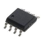
| 描述 | IC OPAMP GP 5.5KHZ RRO 8SOIC |
| 产品分类 | Linear - Amplifiers - Instrumentation, OP Amps, Buffer Amps |
| 品牌 | Texas Instruments |
| 数据手册 | |
| 产品图片 |
|
| 产品型号 | TLV2241IDR |
| rohs | 无铅 / 符合限制有害物质指令(RoHS)规范要求 |
| 产品系列 | - |
| 产品目录页面 | |
| 供应商器件封装 | 8-SOIC |
| 其它名称 | 296-10507-1 |
| 包装 | 剪切带 (CT) |
| 压摆率 | 0.002 V/µs |
| 增益带宽积 | 5.5kHz |
| 安装类型 | 表面贴装 |
| 封装/外壳 | 8-SOIC(0.154",3.90mm 宽) |
| 工作温度 | -40°C ~ 85°C |
| 放大器类型 | 通用 |
| 标准包装 | 1 |
| 电压-电源,单/双 (±) | 2.5 V ~ 12 V, ±1.25 V ~ 6 V |
| 电压-输入失调 | 600µV |
| 电流-电源 | 1µA |
| 电流-输入偏置 | 100pA |
| 电流-输出/通道 | 200µA |
| 电路数 | 1 |
| 输出类型 | 满摆幅 |


- 商务部:美国ITC正式对集成电路等产品启动337调查
- 曝三星4nm工艺存在良率问题 高通将骁龙8 Gen1或转产台积电
- 太阳诱电将投资9.5亿元在常州建新厂生产MLCC 预计2023年完工
- 英特尔发布欧洲新工厂建设计划 深化IDM 2.0 战略
- 台积电先进制程称霸业界 有大客户加持明年业绩稳了
- 达到5530亿美元!SIA预计今年全球半导体销售额将创下新高
- 英特尔拟将自动驾驶子公司Mobileye上市 估值或超500亿美元
- 三星加码芯片和SET,合并消费电子和移动部门,撤换高东真等 CEO
- 三星电子宣布重大人事变动 还合并消费电子和移动部门
- 海关总署:前11个月进口集成电路产品价值2.52万亿元 增长14.8%


PDF Datasheet 数据手册内容提取
TLV2241, TLV2242, TLV2244 FAMILY OF 1-m A/Ch RAIL-TO-RAIL INPUT/OUTPUT OPERATIONAL AMPLIFIERS SLOS329C – JULY 2000 REVISED - NOVEMBER 2000 (cid:0) Micropower Operation... 1 m A/Channel Operational Amplifier (cid:0) Rail-to-Rail Input/Output (cid:0) + Gain Bandwidth Product... 5.5 kHz (cid:0) – Supply Voltage Range... 2.5 V to 12 V (cid:0) Specified Temperature Range – T = 0°C to 70°C... Commercial Grade A SUPPLY CURRENT – TA = –40°C to 125°C... Industrial Grade vs (cid:0) Ultrasmall Packaging SUPPLY VOLTAGE 1.4 – 5-Pin SOT-23 (TLV2241) AV = 1 (cid:0) – 8-Pin MSOP (TLV2242) A/Ch 1.2 VTAIN = =2 5V °CCC / 2 Universal OpAmp EVM m– 1.0 nt e description urr 0.8 C y pl 0.6 The TLV224x family of single-supply operational p u S amplifiers offers very low supply current of only – 0.4 C 1 m A per channel. C I 0.2 The low supply current is coupled with extremely 0 low input bias currents enabling them to be used 0 2 4 6 8 10 12 with mega-W resistors making them ideal for VCC – Supply Voltage – V portable, long active life, applications. DC accuracy is ensured with a low typical offset voltage as low as 600 m V, CMRR of 100 dB, and minimum open loop gain of 100 V/mV at 2.7 V. The maximum recommended supply voltage is as high as 12 V and ensured operation down to 2.5 V, with electrical characteristics specified at 2.7 V, 5 V and 12 V. The 2.5-V operation makes it compatible with Li-Ion battery-powered systems and many micropower microcontrollers available today including TI’s MSP430. FAMILY PACKAGE TABLE PACKAGE TYPES UNIVERSAL DDEEVVIICCEE NNOO. OOFF CChh PDIP SOIC SOT-23 TSSOP MSOP EVM TLV2241 1 8 8 5 — — RReeffeerr ttoo tthhee EEVVMM TLV2242 2 8 8 — — 8 Selection Guide (Lit# SLOU060) TLV2244 4 14 14 — 14 — SELECTION OF SINGLE SUPPLY OPERATIONAL AMPLIFIER PRODUCTS† VDD VIO BW SLEW RATE IDD (PER CHANNEL) DEVICE RAIL-TO-RAIL (V) (mV) (MHz) (V/m s) (m A) TLV240x‡ 2.5–16 0.390 0.005 0.002 0.880 I/O TLV224x 2.5–12 0.600 0.005 0.002 1 I/O TLV2211 2.7–10 0.450 0.065 0.025 13 O TLV245x 2.7–6 0.020 0.22 0.110 23 I/O TLV225x 2.7–8 0.200 0.2 0.12 35 O †All specifications are typical values measured at 5 V. ‡This device also offers 18-V reverse battery protection and 5-V over-the-rail operation on the inputs. Please be aware that an important notice concerning availability, standard warranty, and use in critical applications of TexasInstruments semiconductor products and disclaimers thereto appears at the end of this data sheet. PRODUCTION DATA information is current as of publication date. Copyright 2000, Texas Instruments Incorporated Products conform to specifications per the terms of Texas Instruments standard warranty. Production processing does not necessarily include testing of all parameters. POST OFFICE BOX 655303 • DALLAS, TEXAS 75265 1
TLV2241, TLV2242, TLV2244 FAMILY OF 1-m A/Ch RAIL-TO-RAIL INPUT/OUTPUT OPERATIONAL AMPLIFIERS SLOS329C – JULY 2000 REVISED - NOVEMBER 2000 TLV2241 AVAILABLE OPTIONS PACKAGED DEVICES TA AVVTIO 2mm5aa°Cxx SMALL OUTLINE† SOT-23‡ SYMBOLS PLASTIC DIP (D) (DBV) (P) 0°C to 70°C TLV2241CD — — — 33000000 mm VV –40°C to 125°C TLV2241ID TLV2241IDBV VBEI TLV2241IP †This package is available taped and reeled. To order this packaging option, add an R suffix to the part number (e.g., TLV2241CDR). ‡This package is available in a 250 piece mini-reel. To order this package, add a T suffix to the part number (e.g., TLV2241DBVT). This package is also available in a 3000 piece reel, add a R suffix to the part number (e.g., TLV2241DBVR). TLV2242 AVAILABLE OPTIONS PACKAGED DEVICES TA AVVTIO 2mm5aa°Cxx SMALL OUTLINE† MSOP† SYMBOLS PLASTIC DIP (D) (DGK) (P) 0°C to 70°C TLV2242CD — — — 33000000 mm VV –40°C to 125°C TLV2242ID TLV2242IDGK xxTIALE TLV2242IP †This package is available taped and reeled. To order this packaging option, add an R suffix to the part number (e.g., TLV2242CDR). TLV2244 AVAILABLE OPTIONS PACKAGED DEVICES TA AVVTIO 2mm5aa°Cxx SMALL OUTLINE† PLASTIC DIP TSSOP (D) (N) (PW) 0°C to 70°C TLV2244CD — — 33000000 mm VV –40°C to 125°C TLV2244ID TLV2244IN TLV2244IPW †This package is available taped and reeled. To order this packaging option, add an R suffix to the part number (e.g., TLV2244CDR). TLV224x PACKAGE PINOUTS TLV2241 TLV2241 TLV2242 DBV PACKAGE D OR P PACKAGE D, DGK, OR P PACKAGE (TOP VIEW) (TOP VIEW) (TOP VIEW) OUT 1 5 VCC NC 1 8 NC 1OUT 1 8 VCC IN– 2 7 VCC 1IN– 2 7 2OUT GND 2 IN+ 3 6 OUT 1IN+ 3 6 2IN– GND 4 5 NC GND 4 5 2IN+ IN+ 3 4 IN– NC – No internal connection TLV2244 D, N, OR PW PACKAGE (TOP VIEW) 1OUT 1 14 4OUT 1IN– 2 13 4IN– 1IN+ 3 12 4IN+ VCC 4 11 GND 2IN+ 5 10 3IN+ 2IN– 6 9 3IN– 2OUT 7 8 3OUT 2 POST OFFICE BOX 655303 • DALLAS, TEXAS 75265
TLV2241, TLV2242, TLV2244 FAMILY OF 1-m A/Ch RAIL-TO-RAIL INPUT/OUTPUT OPERATIONAL AMPLIFIERS SLOS329C – JULY 2000 REVISED - NOVEMBER 2000 absolute maximum ratings over operating free-air temperature range (unless otherwise noted)† Supply voltage, V (see Note 1) . . . . . . . . . . . . . . . . . . . . . . . . . . . . . . . . . . . . . . . . . . . . . . . . . . . . . . . . . . 16.5 V CC Differential input voltage, V . . . . . . . . . . . . . . . . . . . . . . . . . . . . . . . . . . . . . . . . . . . . . . . . . . . . . . . . . . . . . . ± V ID CC Input current, I (any input) . . . . . . . . . . . . . . . . . . . . . . . . . . . . . . . . . . . . . . . . . . . . . . . . . . . . . . . . . . . . . . . ±10 mA I Output current, I . . . . . . . . . . . . . . . . . . . . . . . . . . . . . . . . . . . . . . . . . . . . . . . . . . . . . . . . . . . . . . . . . . . . . . . ±10 mA O Continuous total power dissipation . . . . . . . . . . . . . . . . . . . . . . . . . . . . . . . . . . . . . See Dissipation Rating Table Operating free-air temperature range, T : C suffix . . . . . . . . . . . . . . . . . . . . . . . . . . . . . . . . . . . . . . 0°C to 70°C A I suffix . . . . . . . . . . . . . . . . . . . . . . . . . . . . . . . . . . . . –40°C to 125°C Maximum junction temperature, T . . . . . . . . . . . . . . . . . . . . . . . . . . . . . . . . . . . . . . . . . . . . . . . . . . . . . . . . . 150°C J Storage temperature range, T . . . . . . . . . . . . . . . . . . . . . . . . . . . . . . . . . . . . . . . . . . . . . . . . . . . –65°C to 150°C stg Lead temperature 1,6 mm (1/16 inch) from case for 10 seconds . . . . . . . . . . . . . . . . . . . . . . . . . . . . . . . 260°C †Stresses beyond those listed under “absolute maximum ratings” may cause permanent damage to the device. These are stress ratings only, and functional operation of the device at these or any other conditions beyond those indicated under “recommended operating conditions” is not implied. Exposure to absolute-maximum-rated conditions for extended periods may affect device reliability. NOTE 1: All voltage values, except differential voltages, are with respect to GND DISSIPATION RATING TABLE PPAACCKKAAGGEE Q JJCC Q JJAA TAA ≤ 25°C TAA = 125°C (°C/W) (°C/W) POWER RATING POWER RATING D (8) 38.3 176 710 mW 142 mW D (14) 26.9 122.6 1022 mW 204.4 mW DBV (5) 55 324.1 385 mW 77.1 mW DGK (8) 54.2 259.9 481 mW 96.2 mW N (14) 32 78 1600 mW 320.5 mW P (8) 41 104 1200 mW 240.4 mW PW (14) 29.3 173.6 720 mW 144 mW recommended operating conditions MIN MAX UNIT Single supply 2.5 12 SSuuppppllyy vvoollttaaggee, VVCCCC VV Split supply ±1.25 ±6 Common-mode input voltage range, VICR 0 VCC V C-suffix 0 70 OOppeerraattiinngg ffrreeee-aaiirr tteemmppeerraattuurree, TTAA °°CC I-suffix –40 125 POST OFFICE BOX 655303 • DALLAS, TEXAS 75265 3
TLV2241, TLV2242, TLV2244 FAMILY OF 1-m A/Ch RAIL-TO-RAIL INPUT/OUTPUT OPERATIONAL AMPLIFIERS SLOS329C – JULY 2000 REVISED - NOVEMBER 2000 electrical characteristics at recommended operating conditions, V = 2.7, 5 V, and 12 V (unless CC otherwise noted)‡ dc performance PARAMETER TEST CONDITIONS TA† MIN TYP MAX UNIT 25°C 600 3000 VVIIOO IInnppuutt ooffffsseett vvoollttaaggee VVO = VVCC//22 VV, Full range 4500 mm VV VVIICC == VVCCCC//22 VV, RRSS == 5500 WW a VIO Offset voltage drift 25°C 3 m V/°C 25°C 55 100 VVCCCC == 22.77 VV Full range 50 25°C 60 100 CCMMRRRR CCoommmmoonn-mmooddee rreejjeeccttiioonn rraattiioo VVIICC == 00 ttoo VVCCCC, RRSS == 5500WW VVCCCC == 55 VV ddBB Full range 53 25°C 60 100 VVCCCC == 1122 VV Full range 55 25°C 100 400 VVCCCC == 22.77 VV, VVOO((pp)) == 11 VV, RRLL == 550000 kkWW Full range 30 Largge-siggnal differential voltagge 25°C 250 1000 AAVVDD VVCCCC == 55 VV, VVOO((pp)) == 33 VV, RRLL == 550000 kkWW VV//mmVV amplification Full range 100 25°C 700 1500 VVCCCC == 1122 VV, VVOO((pp)) == 66 VV, RRLL == 550000 kkWW Full range 120 †Full range is 0°C to 70°C for the C suffix and –40°C to 125°C for the I suffix. If not specified, full range is –40°C to 125°C. input characteristics PARAMETER TEST CONDITIONS TA† MIN TYP MAX UNIT 25°C 25 250 IIO Input offset current TLV224xC 300 pA FFuullll rraannggee VOO = VCCCC/2 V,, TLV224xI 400 VIC = VCC/2 V, RS = 50 W 25°C 100 500 IIB Input bias current TLV224xC 550 pA FFuullll rraannggee TLV224xI 1000 ri(d) Differential input resistance 25°C 300 MW Ci(c) Common-mode input capacitance f = 100 kHz 25°C 3 pF †Full range is 0°C to 70°C for the C suffix and –40°C to 125°C for the I suffix. If not specified, full range is –40°C to 125°C. ‡Specifications at 5 V are ensured by design and device testing at 2.7 V and 12 V. 4 POST OFFICE BOX 655303 • DALLAS, TEXAS 75265
TLV2241, TLV2242, TLV2244 FAMILY OF 1-m A/Ch RAIL-TO-RAIL INPUT/OUTPUT OPERATIONAL AMPLIFIERS SLOS329C – JULY 2000 REVISED - NOVEMBER 2000 electrical characteristics at recommended operating conditions, V = 2.7, 5 V, and 12 V (unless CC otherwise noted)‡ (continued) output characteristics PARAMETER TEST CONDITIONS TA† MIN TYP MAX UNIT 25°C 2.65 2.68 VVCCCC == 22.77 VV Full range 2.63 VIOIICCH == V–2CC CCm A/2,, VVCCCC == 55 VV Fu2ll 5ra°Cnge 44..9953 4.98 25°C 11.95 11.98 VVCCCC == 1122 VV Full range 11.93 VVOOHH HHiigghh-lleevveell oouuttppuutt vvoollttaaggee VV 25°C 2.62 2.65 VVCCCC == 22.77 VV Full range 2.6 VIOIICCH == V–5CC0CC m/2A,, VVCCCC == 55 VV Fu2ll 5ra°Cnge 44.9.92 4.95 25°C 11.92 11.95 VVCCCC == 1122 VV Full range 11.9 25°C 90 150 VVIICC == VVCCCC//22, IIOOLL == 22 mm AA Full range 180 VVOOLL LLooww-lleevveell oouuttppuutt vvoollttaaggee mmVV 25°C 180 230 VVIICC == VVCCCC//22, IIOOLL == 5500 mm AA Full range 260 IO Output current VO = 0.5 V from rail 25°C ±200 m A †Full range is 0°C to 70°C for the C suffix and –40°C to 125°C for the I suffix. If not specified, full range is –40°C to 125°C. power supply PARAMETER TEST CONDITIONS TA† MIN TYP MAX UNIT 25°C 980 1200 VVCCCC == 22.77 VV oorr 55 VV Full range 1500 IICCCC SSuuppppllyy ccuurrrreenntt ((ppeerr cchhaannnneell)) VVOO == VVCCCC//22 nnAA 25°C 1000 1250 VVCCCC == 1122 VV Full range 1550 25°C 70 100 VVCCCC == 22..77 ttoo 55 VV,, ddBB VIC = VCC/2 V, TLV224xC 65 PPoowweerr ssuuppppllyy rreejjeeccttiioonn rraattiioo No load, FFuullll rraannggee PSRR ((DD VVCCCC//DD VVIIOO)) TLV224xI 60 dB VCCCC = 5 to 12 V, VIICC = VCCCC/2 V, 25°C 70 100 ddBB No load Full range 70 †Full range is 0°C to 70°C for the C suffix and –40°C to 125°C for the I suffix. If not specified, full range is –40°C to 125°C. ‡Specifications at 5 V are ensured by design and device testing at 2.7 V and 12 V. POST OFFICE BOX 655303 • DALLAS, TEXAS 75265 5
TLV2241, TLV2242, TLV2244 FAMILY OF 1-m A/Ch RAIL-TO-RAIL INPUT/OUTPUT OPERATIONAL AMPLIFIERS SLOS329C – JULY 2000 REVISED - NOVEMBER 2000 electrical characteristics at recommended operating conditions, V = 2.7, 5 V, and 12 V (unless CC otherwise noted)‡ (continued) dynamic performance PARAMETER TEST CONDITIONS TA MIN TYP MAX UNIT UGBW Unity gain bandwidth RL = 500 kW , CL = 100 pF 25°C 5.5 kHz SR Slew rate at unity gain VO(pp) = 0.8 V, RL = 500 kW , CL = 100 pF 25°C 2 V/ms f M Phase margin 60 RRLL == 550000 kkWW , CCLL == 110000 ppFF 2255°°CC Gain margin 15 dB VCC = 2.7 or 5 V, V(STEP)PP = 1 V, CL = 100 pF, 0.1% 1.84 AV = –1, RL = 100 kW tts SSeettttlliinngg ttiimmee 2255°°CC mmss VCC = 12 V, 0.1% 6.1 VV((SSTTEEPP))PPPP == 11 VV, CCLL == 110000 pFF, AV = –1, RL = 100 kW 0.01% 32 noise/distortion performance PARAMETER TEST CONDITIONS TA MIN TYP MAX UNIT f = 10 Hz 800 VVn EEqquuiivvaalleenntt iinnppuutt nnooiissee vvoollttaaggee nnVV//√√HHzz f = 100 Hz 25°C 500 In Equivalent input noise current f = 100 Hz 8 fA/√Hz ‡Specifications at 5 V are ensured by design and device testing at 2.7 V and 12 V. 6 POST OFFICE BOX 655303 • DALLAS, TEXAS 75265
TLV2241, TLV2242, TLV2244 FAMILY OF 1-m A/Ch RAIL-TO-RAIL INPUT/OUTPUT OPERATIONAL AMPLIFIERS SLOS329C – JULY 2000 REVISED - NOVEMBER 2000 TYPICAL CHARACTERISTICS Table of Graphs FIGURE VIO Input offset voltage vs Common-mode input voltage 1, 2, 3 vs Free-air temperature 4, 6, 8 IIIIBB IInnppuutt bbiiaass ccuurrrreenntt vs Common-mode input voltage 5, 7, 9 vs Free-air temperature 4, 6, 8 IIIIOO IInnppuutt ooffffsseett ccuurrrreenntt vs Common-mode input voltage 5, 7, 9 CMRR Common-mode rejection ratio vs Frequency 10 VOH High-level output voltage vs High-level output current 11, 13, 15 VOL Low-level output voltage vs Low-level output current 12, 14, 16 VO(PP) Output voltage peak-to-peak vs Frequency 17 Zo Output impedance vs Frequency 18 ICC Supply current vs Supply voltage 19 PSRR Power supply rejection ratio vs Frequency 20 AVD Differential voltage gain vs Frequency 21 Phase vs Frequency 21 Gain-bandwidth product vs Supply voltage 22 SR Slew rate vs Free-air temperature 23 f m Phase margin vs Capacitive load 24 Gain margin vs Capacitive load 25 Voltage noise over a 10 Second Period 26 Large-signal voltage follower 27, 28, 29 Small-signal voltage follower 30 Large-signal inverting pulse response 31, 32, 33 Small-signal inverting pulse response 34 Crosstalk vs Frequency 35 POST OFFICE BOX 655303 • DALLAS, TEXAS 75265 7
TLV2241, TLV2242, TLV2244 FAMILY OF 1-m A/Ch RAIL-TO-RAIL INPUT/OUTPUT OPERATIONAL AMPLIFIERS SLOS329C – JULY 2000 REVISED - NOVEMBER 2000 TYPICAL CHARACTERISTICS INPUT OFFSET VOLTAGE INPUT OFFSET VOLTAGE INPUT OFFSET VOLTAGE vs vs vs COMMON-MODE INPUT COMMON-MODE INPUT COMMON-MODE INPUT VOLTAGE VOLTAGE VOLTAGE 1400 100 400 m– Input Offset Voltage – V 11022468000000000000 VTAC C= 2=5 2°.C7 V m– Input Offset Voltage – V ––2100000 m– Input Offset Voltage – V––2112300000000000 VTAC C= 2=51 2° CV O O–300 O VI 0 VI VCC = 5 V VI–300 TA = 25 °C –200 –400 –400 0.0 0.4 0.8 1.2 1.6 2.0 2.4 2.7 0 1 2 3 4 5 0 2 4 6 8 10 12 VICR – Common-Mode Input Voltage – V VICR – Common-Mode Input Voltage – V VICR – Common-Mode Input Voltage –V Figure 1 Figure 2 Figure 3 INPUT BIAS / OFFSET CURRENT INPUT BIAS / OFFSET CURRENT vs INPUT BIAS / OFFSET CURRENT vs COMMON MODE INPUT vs FREE-AIR TEMPERATURE VOLTAGE FREE-AIR TEMPERATURE 600 400 600 I/I– Input Bias / Offset Current – pAIBIO––2112345000000000000000–40–2VV5CIC–C1 = 0= 1 2.53.75 VV20 II3IIOB5 50 65 80 95110125 I/I– Input Bias / Offset Current – pAIBIO––11–112233505050505500000000000– 00..20 0VTA.C2 C= 2=05 .26 °.7C V1IIII.OB0 1.4 1.8 2.2 2.62.9 I/I– Input Bias / Offset Current – pAIBIO––2112345000000000000000–40–2VV5CIC–C1 = 0= 2 5.55 V V20 II3IIOB5 50 65 80 95110125 TA – Free-Air Temperature – °C VICR – Common Mode Input Voltage – V TA – Free-Air Temperature – °C Figure 4 Figure 5 Figure 6 INPUT BIAS / OFFSET CURRENT INPUT BIAS / OFFSET CURRENT vs INPUT BIAS / OFFSET CURRENT vs COMMON-MODE INPUT vs COMMON-MODE INPUT VOLTAGE FREE-AIR TEMPERATURE VOLTAGE 200 700 250 I/I– Input Bias / Offset Current – pAIBIO––11–115050550000000–00..02 0VT.4AC C=1 2=.05 5 ° VC1.6IIIIOB2.2 2.8 3.4 4.0 4.6 5.2 I/I– Input Bias / Offset Current – pAIBIO––2112345600000000000000000–40–2VV5CIC–C1 = 0= 7 1.552 VV20 I3IO5IIB50 65 80 95110125 I/I– Input Bias / Offset Current – pAIBIO––11–1125050505000000000 VTAC2 C= 2=51 2° CV4 IIOIIB6 8 10 12 VICR – Common Mode Input Voltage – V TA – Free-Air Temperature – °C VICR – Common-Mode Input Voltage –V Figure 7 Figure 8 Figure 9 8 POST OFFICE BOX 655303 • DALLAS, TEXAS 75265
TLV2241, TLV2242, TLV2244 FAMILY OF 1-m A/Ch RAIL-TO-RAIL INPUT/OUTPUT OPERATIONAL AMPLIFIERS SLOS329C – JULY 2000 REVISED - NOVEMBER 2000 TYPICAL CHARACTERISTICS COMMON-MODE REJECTION RATIO HIGH-LEVEL OUTPUT VOLTAGE LOW-LEVEL OUTPUT VOLTAGE vs vs vs FREQUENCY HIGH-LEVEL OUTPUT CURRENT LOW-LEVEL OUTPUT CURRENT B120 2.7 1.50 R – Common-Mode Rejection Ratio – d10246800000 VRRCFI==C11= k02W0.7 k,W 5, 12 V – High-Level Output Voltage – VOH 1122....5814 VCC = 2.7 VTTTTTAAAAA ===== 271––50204 5°0°°C °CC°CC V– Low-Level Output Voltage – VOL 00011.....2570250505 VTTTTTAAACAA C===== 2 0–=715 4 02° 2°0 5C.°C°7 C°C CV R V CM 0 1.2 0 1 10 100 1k 10k 0 50 100 150 200 0 50 100 150 200 f – Frequency – Hz IOH – High-Level Output Current – m A IOL – Low-Level Output Current – m A Figure 10 Figure 11 Figure 12 HIGH-LEVEL OUTPUT VOLTAGE LOW-LEVEL OUTPUT VOLTAGE HIGH-LEVEL OUTPUT VOLTAGE vs vs vs HIGH-LEVEL OUTPUT CURRENT LOW-LEVEL OUTPUT CURRENT HIGH-LEVEL OUTPUT CURRENT 5.0 1.50 15.0 – High-Level Output Voltage – V 344...505 VCC = 5 V TTTTTAAAAA ===== 271––50204 5°0°°C CC°°CC – Low-Level Output Voltage – VL 00011.....2570250505 VTTTTTAACAAA C===== =0–271 4502°50 5C °°V° CC°CC – High-Level Output Voltage – V 111344...505 TTTTAAAA ==== 271–5020 5°°°C CC°CTA = –40°C H O H O V O V V VCC = 12 V 3.0 0 13 0 50 100 150 200 0 50 100 150 200 0 50 100 150 200 IOH – High-Level Output Current – m A IOL – Low-Level Output Current – m A IOH – High-Level Output Current – m A Figure 13 Figure 14 Figure 15 OUTPUT VOLTAGE LOW-LEVEL OUTPUT VOLTAGE PEAK-TO-PEAK OUTPUT IMPEDANCE vs vs vs LOW-LEVEL OUTPUT CURRENT FREQUENCY FREQUENCY 1.50 V 16 10k – Low-Level Output Voltage – VL 00011.....2570250505 VTCAC = = – 1420 °VC TTTTAAAA ==== 271–5020 5°°°C CC°C – Output voltage Peak–to–Peak – 1110242468 VVCCCC = = 5 V2 V.C7C V = 12 V RCTALL === 211500°00C kpWF W– Output Impedance –Zo1010k AV=10 AV=1 VO O(PP) 0 VTAC=C2=52°.C7, 5, 12 V 0 V –2 10 0 50 100 150 200 10 100 1k 100 1k 10k IOL – Low-Level Output Current – m A f – Frequency – Hz f – Frequency – Hz Figure 16 Figure 17 Figure 18 POST OFFICE BOX 655303 • DALLAS, TEXAS 75265 9
TLV2241, TLV2242, TLV2244 FAMILY OF 1-m A/Ch RAIL-TO-RAIL INPUT/OUTPUT OPERATIONAL AMPLIFIERS SLOS329C – JULY 2000 REVISED - NOVEMBER 2000 TYPICAL CHARACTERISTICS SUPPLY CURRENT POWER SUPPLY REJECTION RATIO vs vs SUPPLY VOLTAGE FREQUENCY 1.4 B 120 d m– A/Ch 11..02 on Ratio – 110100 VTAC C= 2=5 2°.C7, 5, & 12 V urrent 0.8 Rejecti 90 ISupply C–CC 000...246 AV = 1 TTTTTAAAAA ===== 2 071–5 024° °50C°C°°CCC R – Power Supply 56780000 VIN = VCC / 2 SR 0 P 40 0 2 4 6 8 10 12 10 100 1k 10k VCC – Supply Voltage – V f – Frequency – Hz Figure 19 Figure 20 DIFFERENTIAL VOLTAGE GAIN AND PHASE GAIN BANDWIDTH PRODUCT vs vs FREQUENCY SUPPLY VOLTAGE 7 60 135 Hz TA = 25°C ential Voltage Gain – dB 1324500000 4950 °Phase – n Bandwidth Product – k 3456 RCf =LL 1==k 11H00z00 kpWF er ai 2 – DiffAVD–100 VRCTACLL===C512=005200°.C 7kp,WF 5, 12 V 0 GBWP –G 1 –20 –45 0 10 100 1k 10k 2 3 4 5 6 7 8 9 10 11 12 f – Frequency – Hz VCC – Supply Voltage –V Figure 21 Figure 22 SLEW RATE PHASE MARGIN vs vs FREE-AIR TEMPERATURE CAPACITIVE LOAD 3.5 80 3.0 SR+ 70 s m VCC = 5, 12 V 60 w Rate – V/ 22..05 VCC = 2.7 V °Margin – 4500 – Sle 1.5 ase 30 SR 1.0 SR– VCC = 2.7, 5, 12 V Ph VCC = 2.7, 5, & 12 V 20 RL= 500 kW 0.5 10 TA = 25°C 0 0 –40–25–10 5 20 35 50 65 80 95110125 10 100 1k 10k TA – Free-Air Temperature – °C CL – Capacitive Load – pF Figure 23 Figure 24 10 POST OFFICE BOX 655303 • DALLAS, TEXAS 75265
TLV2241, TLV2242, TLV2244 FAMILY OF 1-m A/Ch RAIL-TO-RAIL INPUT/OUTPUT OPERATIONAL AMPLIFIERS SLOS329C – JULY 2000 REVISED - NOVEMBER 2000 TYPICAL CHARACTERISTICS GAIN MARGIN VOLTAGE NOISE vs OVER A 10 SECOND PERIOD CAPACITIVE LOAD 25 4 RL= 500 kW VCC = 5 V 20 TA = 25°C m– V 3 fT A= 0=. 12 5H°zC to 10 Hz se 2 B oi – d 15 VCC = 12 V e N 1 Gain Margin 10 erred Voltag –10 VCC = 2.7, 5 V Ref –2 5 ut p n –3 I 0 –4 10 100 1k 10k 0 1 2 3 4 5 6 7 8 9 10 CL – Capacitive Load – pF t – Time – s Figure 25 Figure 26 LARGE SIGNAL FOLLOWER LARGE SIGNAL FOLLOWER PULSE RESPONSE PULSE RESPONSE V– Input Voltage – VIN–––321012 VINVO VARCTAVCLL C==== 21=11500 2°00.C 7kp WVF 012 Output Voltage – V V– Input Voltage – VIN–103421012345678 VIN VO VARCTAVCLL C==== 21=11500 5°00 C VkpWF 03421 – Output Voltage – V –4–1 0 1 2 3 4 5 6 V– O –1 VO –1 0 1 2 3 4 5 6 t – Time – ms t – Time – ms Figure 27 Figure 28 LARGE SIGNAL FOLLOWER SMALL SIGNAL FOLLOWER PULSE RESPONSE PULSE RESPONSE V 3105 V 310800 V– Input Voltage – IN 1122–1500505505 VIN VO VARCTAVCLL C==== 21=11500 1°002C kp VWF 11505 ut Voltage – V V– Input Voltage – mIN –1111115502464680000000000 VVINO V&AR TCAV CL1L C=2 === V=21 115 020°0.0C7 k,p W5F, 116842000000 put Voltage – mV 0 0 – OutpO 200 200 V– OutO V –5 –20 –2 0 2 4 6 8 10 12 14 16 0 100 200 300 400 500 t – Time – ms t – Time – m s Figure 29 Figure 30 POST OFFICE BOX 655303 • DALLAS, TEXAS 75265 11
TLV2241, TLV2242, TLV2244 FAMILY OF 1-m A/Ch RAIL-TO-RAIL INPUT/OUTPUT OPERATIONAL AMPLIFIERS SLOS329C – JULY 2000 REVISED - NOVEMBER 2000 TYPICAL CHARACTERISTICS LARGE SIGNAL INVERTING LARGE SIGNAL INVERTING PULSE RESPONSE PULSE RESPONSE V 2 3.0 – V 2 4.5 V– Input Voltage – IN–––100011 1120......050505 VARCTAVCLL C====V 2=–11IN5100 2°00.C 7kp WVF ––0001..05..50 put Voltage – V V– Input Voltage IN–––––211000112 12301.........050505050 VVARCTAVICLLN C==== 2=–115100 5°00 C VkpWF ––––011200......505050 utput Voltage – V –1.5 VO –1.5 – OutO ––32..05 VO ––32..05 V– OO –2 –2.0 V –3.5 –3.5 –1 0 1 2 3 4 5 6 7 –1 0 1 2 3 4 5 6 7 t – Time – ms t – Time – ms Figure 31 Figure 32 LARGE SIGNAL INVERTING SMALL SIGNAL INVERTING PULSE RESPONSE PULSE RESPONSE V 1122 mV 220000 V– Input Voltage – IN –––1 3690342002468 VAR TCAVCLL C==V == I2–= 1N1510 01°002C k pVWF ––2420 Voltage – V V– Input Voltage – IN–11 11 00 055 0000000 V&AR TCAV CL1L C=2= ==V V=2– 1I15 N1020°0.0C7 k ,p W5F, 500 oltage – mV –1––086 VO –––1680 – Output O –1–0500 VO –1–0500 – Output V V O –12 –12 –150 –150 V –5 0 5 10 15 20 25 30 35 –200 0 200 400 600 800 1000 1200 t – Time – ms t – Time – ms Figure 33 Figure 34 CROSSTALK vs FREQUENCY 0 VCC = 2.7, –20 5, & 12 V All Channels –40 RL = 100 kW – dB –60 CVILN = = 1 10 0V PpFP VCC = 12V k al st –80 s o Cr –100 VCC = 2.7, 5 V –120 –140 10 100 1k 10k f – Frequency –Hz Figure 35 12 POST OFFICE BOX 655303 • DALLAS, TEXAS 75265
TLV2241, TLV2242, TLV2244 FAMILY OF 1-m A/Ch RAIL-TO-RAIL INPUT/OUTPUT OPERATIONAL AMPLIFIERS SLOS329C – JULY 2000 REVISED - NOVEMBER 2000 APPLICATION INFORMATION offset voltage The output offset voltage, (V ) is the sum of the input offset voltage (V ) and both input bias currents (I ) times OO IO IB the corresponding gains. The following schematic and formula can be used to calculate the output offset voltage: RF IIB– (cid:3) (cid:3)RF(cid:4)(cid:4) (cid:3) (cid:3)RF(cid:4)(cid:4) RG VOO(cid:2)VIO 1(cid:1) RG (cid:0)IIB(cid:1) RS 1(cid:1) RG (cid:0)IIB– RF + – VI VO + RS IIB+ Figure 36. Output Offset Voltage Model general configurations When receiving low-level signals, limiting the bandwidth of the incoming signals into the system is often required. The simplest way to accomplish this is to place an RC filter at the noninverting terminal of the amplifier (see Figure 37). RG RF 1 f–3dB (cid:2) 2(cid:0)R1C1 VI +– VO VVOI (cid:2) (cid:3)1(cid:1)RRGF(cid:4)(cid:3)1(cid:1)s1R1C1(cid:4) R1 C1 Figure 37. Single-Pole Low-Pass Filter If even more attenuation is needed, a multiple pole filter is required. The Sallen-Key filter can be used for this task. For best results, the amplifier should have a bandwidth that is 8 to 10 times the filter frequency bandwidth. Failure to do this can result in phase shift of the amplifier. C1 R1 = R2 = R C1 = C2 = C Q = Peaking Factor (Butterworth Q = 0.707) VI + R1 R2 _ f–3dB (cid:2) 2(cid:0)1RC C2 RF RG = RF (2 – 1 ) RG Q Figure 38. 2-Pole Low-Pass Sallen-Key Filter POST OFFICE BOX 655303 • DALLAS, TEXAS 75265 13
TLV2241, TLV2242, TLV2244 FAMILY OF 1-m A/Ch RAIL-TO-RAIL INPUT/OUTPUT OPERATIONAL AMPLIFIERS SLOS329C – JULY 2000 REVISED - NOVEMBER 2000 APPLICATION INFORMATION circuit layout considerations To achieve the levels of high performance of the TLV224x, follow proper printed-circuit board design techniques. A general set of guidelines is given in the following. (cid:0) Ground planes—It is highly recommended that a ground plane be used on the board to provide all components with a low inductive ground connection. However, in the areas of the amplifier inputs and output, the ground plane can be removed to minimize the stray capacitance. (cid:0) Proper power supply decoupling—Use a 6.8-m F tantalum capacitor in parallel with a 0.1-m F ceramic capacitor on each supply terminal. It may be possible to share the tantalum among several amplifiers depending on the application, but a 0.1-m F ceramic capacitor should always be used on the supply terminal of every amplifier. In addition, the 0.1-m F capacitor should be placed as close as possible to the supply terminal. As this distance increases, the inductance in the connecting trace makes the capacitor less effective. The designer should strive for distances of less than 0.1 inches between the device power terminals and the ceramic capacitors. (cid:0) Sockets—Sockets can be used but are not recommended. The additional lead inductance in the socket pins will often lead to stability problems. Surface-mount packages soldered directly to the printed-circuit board is the best implementation. (cid:0) Short trace runs/compact part placements—Optimum high performance is achieved when stray series inductance has been minimized. To realize this, the circuit layout should be made as compact as possible, thereby minimizing the length of all trace runs. Particular attention should be paid to the inverting input of the amplifier. Its length should be kept as short as possible. This will help to minimize stray capacitance at the input of the amplifier. (cid:0) Surface-mount passive components—Using surface-mount passive components is recommended for high performance amplifier circuits for several reasons. First, because of the extremely low lead inductance of surface-mount components, the problem with stray series inductance is greatly reduced. Second, the small size of surface-mount components naturally leads to a more compact layout thereby minimizing both stray inductance and capacitance. If leaded components are used, it is recommended that the lead lengths be kept as short as possible. 14 POST OFFICE BOX 655303 • DALLAS, TEXAS 75265
TLV2241, TLV2242, TLV2244 FAMILY OF 1-m A/Ch RAIL-TO-RAIL INPUT/OUTPUT OPERATIONAL AMPLIFIERS SLOS329C – JULY 2000 REVISED - NOVEMBER 2000 APPLICATION INFORMATION general power dissipation considerations For a given q , the maximum power dissipation is shown in Figure 39 and is calculated by the following formula: JA (cid:1)TMAX–TA(cid:2) PD(cid:0) (cid:0) JA Where: P = Maximum power dissipation of THS224x IC (watts) D T = Absolute maximum junction temperature (150°C) MAX T = Free-ambient air temperature (°C) A q JA = q JC + q CA q = Thermal coefficient from junction to case JC q = Thermal coefficient from case to ambient air (°C/W) CA MAXIMUM POWER DISSIPATION vs FREE-AIR TEMPERATURE 2 PDIP Package TJ = 150°C 1.75 Low-K Test PCB q JA = 104°C/W W n – 1.5 MSOP Package o pati 1.25 SOIC Package Lq JoAw -=K 2 T6e0s°tC P/WCB si Low-K Test PCB Dis q JA = 176°C/W r 1 e w o P m 0.75 u m xi 0.5 a M 0.25 SOT-23 Package Low-K Test PCB 0 q JA = 324°C/W –55–40–25 –10 5 20 35 50 65 80 95 110 125 TA – Free-Air Temperature – °C NOTE A: Results are with no air flow and using JEDEC Standard Low-K test PCB. Figure 39. Maximum Power Dissipation vs Free-Air Temperature POST OFFICE BOX 655303 • DALLAS, TEXAS 75265 15
TLV2241, TLV2242, TLV2244 FAMILY OF 1-m A/Ch RAIL-TO-RAIL INPUT/OUTPUT OPERATIONAL AMPLIFIERS SLOS329C – JULY 2000 REVISED - NOVEMBER 2000 APPLICATION INFORMATION macromodel information Macromodel information provided was derived using Microsim Parts Release 8, the model generation software used with Microsim PSpice. The Boyle macromodel (see Note 2) and subcircuit in Figure 40 are generated using the TLV224x typical electrical and operating characteristics at T = 25°C. Using this A information, output simulations of the following key parameters can be generated to a tolerance of 20% (in most cases): (cid:0) (cid:0) Maximum positive output voltage swing Unity-gain frequency (cid:0) (cid:0) Maximum negative output voltage swing Common-mode rejection ratio (cid:0) (cid:0) Slew rate Phase margin (cid:0) (cid:0) Quiescent power dissipation DC output resistance (cid:0) (cid:0) Input bias current AC output resistance (cid:0) (cid:0) Open-loop voltage amplification Short-circuit output current limit NOTE 2: G. R. Boyle, B. M. Cohn, D. O. Pederson, and J. E. Solomon, “Macromodeling of Integrated Circuit Operational Amplifiers”, IEEE Journal of Solid-State Circuits, SC-9, 353 (1974). 3 99 VCC+ + rp rc1 rc2 ree cee egnd fb ro2 – c1 7 11 12 + 1 c2 IN+ + 9 r2 6 vlim – vc 2 + 8 IN– q1 q2 – vb ga 53 – gcm ioff ro1 dp 13 14 re1 re2 VOUT dlp dln 10 91 90 92 5 iee dc + + – vlp hlim vln VCC– – – + 4 – ve + 54 de .subckt 224X_5V–X 1 2 3 4 5 rc1 3 11 978.81E3 * rc2 3 12 978.81E3 c1 11 12 9.8944E–12 re1 13 10 30.364E3 c2 6 7 30.000E–12 re2 14 10 30.364E3 cee 10 99 8.8738E–12 ree 10 99 3.6670E9 dc 5 53 dy ro1 8 5 10 de 54 5 dy ro2 7 99 10 dlp 90 91 dx rp 3 4 1.4183E6 dln 92 90 dx vb 9 0 dc 0 dp 4 3 dx vc 3 53 dc .88315 egnd 99 0 poly(2) (3,0) (4,0) 0 .5 .5 ve 54 4 dc .88315 fb 7 99 poly(5) vb vc ve vlp vln 0 61.404E6 –1E3 1E3 61E6 –61E6 vlim 7 8 dc 0 ga 6 0 11 12 1.0216E–6 vlp 91 0 dc 540 gcm 0 6 10 99 10.216E–12 vln 0 92 dc 540 iee 10 4 dc 54.540E–9 .model dx D(Is=800.00E–18) ioff 0 6 dc 5e–12 .model dy D(Is=800.00E–18 Rs=1m Cjo=10p) hlim 90 0 vlim 1K .model qx1 NPN(Is=800.00E–18 Bf=27.270E21) q1 11 2 13 qx1 .model qx2 NPN(Is=800.0000E–18 Bf=27.270E21) q2 12 1 14 qx2 .ends r2 6 9 100.00E3 Figure 40. Boyle Macromodels and Subcircuit PSpice and Parts are trademarks of MicroSim Corporation. 16 POST OFFICE BOX 655303 • DALLAS, TEXAS 75265
PACKAGE OPTION ADDENDUM www.ti.com 6-Feb-2020 PACKAGING INFORMATION Orderable Device Status Package Type Package Pins Package Eco Plan Lead/Ball Finish MSL Peak Temp Op Temp (°C) Device Marking Samples (1) Drawing Qty (2) (6) (3) (4/5) TLV2241ID ACTIVE SOIC D 8 75 Green (RoHS NIPDAU Level-1-260C-UNLIM -40 to 125 2241I & no Sb/Br) TLV2241IDBVR ACTIVE SOT-23 DBV 5 3000 Green (RoHS NIPDAU Level-1-260C-UNLIM -40 to 125 VBEI & no Sb/Br) TLV2241IDBVRG4 ACTIVE SOT-23 DBV 5 3000 Green (RoHS NIPDAU Level-1-260C-UNLIM -40 to 125 VBEI & no Sb/Br) TLV2241IDBVT ACTIVE SOT-23 DBV 5 250 Green (RoHS NIPDAU Level-1-260C-UNLIM -40 to 125 VBEI & no Sb/Br) TLV2241IDR ACTIVE SOIC D 8 2500 Green (RoHS NIPDAU Level-1-260C-UNLIM -40 to 125 2241I & no Sb/Br) TLV2241IP ACTIVE PDIP P 8 50 Green (RoHS NIPDAU N / A for Pkg Type -40 to 125 TLV2241I & no Sb/Br) TLV2242CD ACTIVE SOIC D 8 75 Green (RoHS NIPDAU Level-1-260C-UNLIM 0 to 70 2242C & no Sb/Br) TLV2242CDR ACTIVE SOIC D 8 2500 Green (RoHS NIPDAU Level-1-260C-UNLIM 0 to 70 2242C & no Sb/Br) TLV2242ID ACTIVE SOIC D 8 75 Green (RoHS NIPDAU Level-1-260C-UNLIM -40 to 125 2242I & no Sb/Br) TLV2242IDGK ACTIVE VSSOP DGK 8 80 Green (RoHS NIPDAU Level-1-260C-UNLIM -40 to 125 ALE & no Sb/Br) TLV2242IDGKR ACTIVE VSSOP DGK 8 2500 Green (RoHS NIPDAU Level-1-260C-UNLIM -40 to 125 ALE & no Sb/Br) TLV2242IDGKRG4 ACTIVE VSSOP DGK 8 2500 Green (RoHS NIPDAU Level-1-260C-UNLIM -40 to 125 ALE & no Sb/Br) TLV2242IDR ACTIVE SOIC D 8 2500 Green (RoHS NIPDAU Level-1-260C-UNLIM -40 to 125 2242I & no Sb/Br) TLV2242IP ACTIVE PDIP P 8 50 Green (RoHS NIPDAU N / A for Pkg Type -40 to 125 TLV2242I & no Sb/Br) TLV2244CD ACTIVE SOIC D 14 50 Green (RoHS NIPDAU Level-1-260C-UNLIM 0 to 70 TLV2244C & no Sb/Br) TLV2244ID ACTIVE SOIC D 14 50 Green (RoHS NIPDAU Level-1-260C-UNLIM -40 to 125 TLV2244I & no Sb/Br) TLV2244IDR ACTIVE SOIC D 14 2500 Green (RoHS NIPDAU Level-1-260C-UNLIM -40 to 125 TLV2244I & no Sb/Br) Addendum-Page 1
PACKAGE OPTION ADDENDUM www.ti.com 6-Feb-2020 Orderable Device Status Package Type Package Pins Package Eco Plan Lead/Ball Finish MSL Peak Temp Op Temp (°C) Device Marking Samples (1) Drawing Qty (2) (6) (3) (4/5) TLV2244IN ACTIVE PDIP N 14 25 Green (RoHS NIPDAU N / A for Pkg Type -40 to 125 TLV2244I & no Sb/Br) TLV2244IPW ACTIVE TSSOP PW 14 90 Green (RoHS NIPDAU Level-1-260C-UNLIM -40 to 125 2244I & no Sb/Br) TLV2244IPWR ACTIVE TSSOP PW 14 2000 Green (RoHS NIPDAU Level-1-260C-UNLIM -40 to 125 2244I & no Sb/Br) (1) The marketing status values are defined as follows: ACTIVE: Product device recommended for new designs. LIFEBUY: TI has announced that the device will be discontinued, and a lifetime-buy period is in effect. NRND: Not recommended for new designs. Device is in production to support existing customers, but TI does not recommend using this part in a new design. PREVIEW: Device has been announced but is not in production. Samples may or may not be available. OBSOLETE: TI has discontinued the production of the device. (2) RoHS: TI defines "RoHS" to mean semiconductor products that are compliant with the current EU RoHS requirements for all 10 RoHS substances, including the requirement that RoHS substance do not exceed 0.1% by weight in homogeneous materials. Where designed to be soldered at high temperatures, "RoHS" products are suitable for use in specified lead-free processes. TI may reference these types of products as "Pb-Free". RoHS Exempt: TI defines "RoHS Exempt" to mean products that contain lead but are compliant with EU RoHS pursuant to a specific EU RoHS exemption. Green: TI defines "Green" to mean the content of Chlorine (Cl) and Bromine (Br) based flame retardants meet JS709B low halogen requirements of <=1000ppm threshold. Antimony trioxide based flame retardants must also meet the <=1000ppm threshold requirement. (3) MSL, Peak Temp. - The Moisture Sensitivity Level rating according to the JEDEC industry standard classifications, and peak solder temperature. (4) There may be additional marking, which relates to the logo, the lot trace code information, or the environmental category on the device. (5) Multiple Device Markings will be inside parentheses. Only one Device Marking contained in parentheses and separated by a "~" will appear on a device. If a line is indented then it is a continuation of the previous line and the two combined represent the entire Device Marking for that device. (6) Lead/Ball Finish - Orderable Devices may have multiple material finish options. Finish options are separated by a vertical ruled line. Lead/Ball Finish values may wrap to two lines if the finish value exceeds the maximum column width. Important Information and Disclaimer:The information provided on this page represents TI's knowledge and belief as of the date that it is provided. TI bases its knowledge and belief on information provided by third parties, and makes no representation or warranty as to the accuracy of such information. Efforts are underway to better integrate information from third parties. TI has taken and continues to take reasonable steps to provide representative and accurate information but may not have conducted destructive testing or chemical analysis on incoming materials and chemicals. TI and TI suppliers consider certain information to be proprietary, and thus CAS numbers and other limited information may not be available for release. In no event shall TI's liability arising out of such information exceed the total purchase price of the TI part(s) at issue in this document sold by TI to Customer on an annual basis. Addendum-Page 2
PACKAGE OPTION ADDENDUM www.ti.com 6-Feb-2020 Addendum-Page 3
PACKAGE MATERIALS INFORMATION www.ti.com 23-May-2019 TAPE AND REEL INFORMATION *Alldimensionsarenominal Device Package Package Pins SPQ Reel Reel A0 B0 K0 P1 W Pin1 Type Drawing Diameter Width (mm) (mm) (mm) (mm) (mm) Quadrant (mm) W1(mm) TLV2241IDBVR SOT-23 DBV 5 3000 180.0 9.0 3.15 3.2 1.4 4.0 8.0 Q3 TLV2241IDBVR SOT-23 DBV 5 3000 180.0 8.4 3.2 3.2 1.4 4.0 8.0 Q3 TLV2241IDBVT SOT-23 DBV 5 250 180.0 9.0 3.15 3.2 1.4 4.0 8.0 Q3 TLV2241IDBVT SOT-23 DBV 5 250 180.0 8.4 3.2 3.2 1.4 4.0 8.0 Q3 TLV2241IDR SOIC D 8 2500 330.0 12.4 6.4 5.2 2.1 8.0 12.0 Q1 TLV2242CDR SOIC D 8 2500 330.0 12.4 6.4 5.2 2.1 8.0 12.0 Q1 TLV2242IDGKR VSSOP DGK 8 2500 330.0 12.4 5.3 3.4 1.4 8.0 12.0 Q1 TLV2242IDR SOIC D 8 2500 330.0 12.4 6.4 5.2 2.1 8.0 12.0 Q1 TLV2244IDR SOIC D 14 2500 330.0 16.4 6.5 9.0 2.1 8.0 16.0 Q1 TLV2244IPWR TSSOP PW 14 2000 330.0 12.4 6.9 5.6 1.6 8.0 12.0 Q1 PackMaterials-Page1
PACKAGE MATERIALS INFORMATION www.ti.com 23-May-2019 *Alldimensionsarenominal Device PackageType PackageDrawing Pins SPQ Length(mm) Width(mm) Height(mm) TLV2241IDBVR SOT-23 DBV 5 3000 182.0 182.0 20.0 TLV2241IDBVR SOT-23 DBV 5 3000 210.0 185.0 35.0 TLV2241IDBVT SOT-23 DBV 5 250 182.0 182.0 20.0 TLV2241IDBVT SOT-23 DBV 5 250 210.0 185.0 35.0 TLV2241IDR SOIC D 8 2500 340.5 338.1 20.6 TLV2242CDR SOIC D 8 2500 340.5 338.1 20.6 TLV2242IDGKR VSSOP DGK 8 2500 358.0 335.0 35.0 TLV2242IDR SOIC D 8 2500 340.5 338.1 20.6 TLV2244IDR SOIC D 14 2500 350.0 350.0 43.0 TLV2244IPWR TSSOP PW 14 2000 367.0 367.0 35.0 PackMaterials-Page2
PACKAGE OUTLINE DBV0005A SOT-23 - 1.45 mm max height SCALE 4.000 SMALL OUTLINE TRANSISTOR C 3.0 2.6 0.1 C 1.75 1.45 1.45 B A 0.90 PIN 1 INDEX AREA 1 5 2X 0.95 3.05 2.75 1.9 1.9 2 4 3 0.5 5X 0.3 0.15 0.2 C A B (1.1) TYP 0.00 0.25 GAGE PLANE 0.22 TYP 0.08 8 TYP 0.6 0 0.3 TYP SEATING PLANE 4214839/E 09/2019 NOTES: 1. All linear dimensions are in millimeters. Any dimensions in parenthesis are for reference only. Dimensioning and tolerancing per ASME Y14.5M. 2. This drawing is subject to change without notice. 3. Refernce JEDEC MO-178. 4. Body dimensions do not include mold flash, protrusions, or gate burrs. Mold flash, protrusions, or gate burrs shall not exceed 0.15 mm per side. www.ti.com
EXAMPLE BOARD LAYOUT DBV0005A SOT-23 - 1.45 mm max height SMALL OUTLINE TRANSISTOR PKG 5X (1.1) 1 5 5X (0.6) SYMM (1.9) 2 2X (0.95) 3 4 (R0.05) TYP (2.6) LAND PATTERN EXAMPLE EXPOSED METAL SHOWN SCALE:15X SOLDER MASK SOLDER MASK METAL UNDER METAL OPENING OPENING SOLDER MASK EXPOSED METAL EXPOSED METAL 0.07 MAX 0.07 MIN ARROUND ARROUND NON SOLDER MASK SOLDER MASK DEFINED DEFINED (PREFERRED) SOLDER MASK DETAILS 4214839/E 09/2019 NOTES: (continued) 5. Publication IPC-7351 may have alternate designs. 6. Solder mask tolerances between and around signal pads can vary based on board fabrication site. www.ti.com
EXAMPLE STENCIL DESIGN DBV0005A SOT-23 - 1.45 mm max height SMALL OUTLINE TRANSISTOR PKG 5X (1.1) 1 5 5X (0.6) SYMM 2 (1.9) 2X(0.95) 3 4 (R0.05) TYP (2.6) SOLDER PASTE EXAMPLE BASED ON 0.125 mm THICK STENCIL SCALE:15X 4214839/E 09/2019 NOTES: (continued) 7. Laser cutting apertures with trapezoidal walls and rounded corners may offer better paste release. IPC-7525 may have alternate design recommendations. 8. Board assembly site may have different recommendations for stencil design. www.ti.com
None
None
None
None
PACKAGE OUTLINE D0008A SOIC - 1.75 mm max height SCALE 2.800 SMALL OUTLINE INTEGRATED CIRCUIT C SEATING PLANE .228-.244 TYP [5.80-6.19] .004 [0.1] C A PIN 1 ID AREA 6X .050 [1.27] 8 1 2X .189-.197 [4.81-5.00] .150 NOTE 3 [3.81] 4X (0 -15 ) 4 5 8X .012-.020 B .150-.157 [0.31-0.51] .069 MAX [3.81-3.98] .010 [0.25] C A B [1.75] NOTE 4 .005-.010 TYP [0.13-0.25] 4X (0 -15 ) SEE DETAIL A .010 [0.25] .004-.010 0 - 8 [0.11-0.25] .016-.050 [0.41-1.27] DETAIL A (.041) TYPICAL [1.04] 4214825/C 02/2019 NOTES: 1. Linear dimensions are in inches [millimeters]. Dimensions in parenthesis are for reference only. Controlling dimensions are in inches. Dimensioning and tolerancing per ASME Y14.5M. 2. This drawing is subject to change without notice. 3. This dimension does not include mold flash, protrusions, or gate burrs. Mold flash, protrusions, or gate burrs shall not exceed .006 [0.15] per side. 4. This dimension does not include interlead flash. 5. Reference JEDEC registration MS-012, variation AA. www.ti.com
EXAMPLE BOARD LAYOUT D0008A SOIC - 1.75 mm max height SMALL OUTLINE INTEGRATED CIRCUIT 8X (.061 ) [1.55] SYMM SEE DETAILS 1 8 8X (.024) [0.6] SYMM (R.002 ) TYP [0.05] 5 4 6X (.050 ) [1.27] (.213) [5.4] LAND PATTERN EXAMPLE EXPOSED METAL SHOWN SCALE:8X SOLDER MASK SOLDER MASK METAL OPENING OPENING METAL UNDER SOLDER MASK EXPOSED METAL EXPOSED METAL .0028 MAX .0028 MIN [0.07] [0.07] ALL AROUND ALL AROUND NON SOLDER MASK SOLDER MASK DEFINED DEFINED SOLDER MASK DETAILS 4214825/C 02/2019 NOTES: (continued) 6. Publication IPC-7351 may have alternate designs. 7. Solder mask tolerances between and around signal pads can vary based on board fabrication site. www.ti.com
EXAMPLE STENCIL DESIGN D0008A SOIC - 1.75 mm max height SMALL OUTLINE INTEGRATED CIRCUIT 8X (.061 ) [1.55] SYMM 1 8 8X (.024) [0.6] SYMM (R.002 ) TYP [0.05] 5 4 6X (.050 ) [1.27] (.213) [5.4] SOLDER PASTE EXAMPLE BASED ON .005 INCH [0.125 MM] THICK STENCIL SCALE:8X 4214825/C 02/2019 NOTES: (continued) 8. Laser cutting apertures with trapezoidal walls and rounded corners may offer better paste release. IPC-7525 may have alternate design recommendations. 9. Board assembly site may have different recommendations for stencil design. www.ti.com
None
None
None
None
IMPORTANTNOTICEANDDISCLAIMER TI PROVIDES TECHNICAL AND RELIABILITY DATA (INCLUDING DATASHEETS), DESIGN RESOURCES (INCLUDING REFERENCE DESIGNS), APPLICATION OR OTHER DESIGN ADVICE, WEB TOOLS, SAFETY INFORMATION, AND OTHER RESOURCES “AS IS” AND WITH ALL FAULTS, AND DISCLAIMS ALL WARRANTIES, EXPRESS AND IMPLIED, INCLUDING WITHOUT LIMITATION ANY IMPLIED WARRANTIES OF MERCHANTABILITY, FITNESS FOR A PARTICULAR PURPOSE OR NON-INFRINGEMENT OF THIRD PARTY INTELLECTUAL PROPERTY RIGHTS. These resources are intended for skilled developers designing with TI products. You are solely responsible for (1) selecting the appropriate TI products for your application, (2) designing, validating and testing your application, and (3) ensuring your application meets applicable standards, and any other safety, security, or other requirements. These resources are subject to change without notice. TI grants you permission to use these resources only for development of an application that uses the TI products described in the resource. Other reproduction and display of these resources is prohibited. No license is granted to any other TI intellectual property right or to any third party intellectual property right. TI disclaims responsibility for, and you will fully indemnify TI and its representatives against, any claims, damages, costs, losses, and liabilities arising out of your use of these resources. TI’s products are provided subject to TI’s Terms of Sale (www.ti.com/legal/termsofsale.html) or other applicable terms available either on ti.com or provided in conjunction with such TI products. TI’s provision of these resources does not expand or otherwise alter TI’s applicable warranties or warranty disclaimers for TI products. Mailing Address: Texas Instruments, Post Office Box 655303, Dallas, Texas 75265 Copyright © 2020, Texas Instruments Incorporated