ICGOO在线商城 > 集成电路(IC) > 数据采集 - 模数转换器 > TLC0820AIDW

 Datasheet下载
- 型号: TLC0820AIDW
- 制造商: Texas Instruments
- 库位|库存: xxxx|xxxx
- 要求:
| 数量阶梯 | 香港交货 | 国内含税 |
| +xxxx | $xxxx | ¥xxxx |
查看当月历史价格
查看今年历史价格
TLC0820AIDW产品简介:
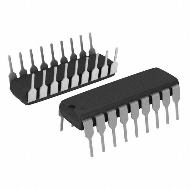
ICGOO电子元器件商城为您提供TLC0820AIDW由Texas Instruments设计生产,在icgoo商城现货销售,并且可以通过原厂、代理商等渠道进行代购。 TLC0820AIDW价格参考¥19.50-¥36.23。Texas InstrumentsTLC0820AIDW封装/规格:数据采集 - 模数转换器, 8 Bit Analog to Digital Converter 1 Input 1 Flash 20-SOIC。您可以下载TLC0820AIDW参考资料、Datasheet数据手册功能说明书,资料中有TLC0820AIDW 详细功能的应用电路图电压和使用方法及教程。
TLC0820AIDW是德州仪器(Texas Instruments)生产的一款8位、20 MSPS(百万次采样每秒)的模数转换器(ADC),广泛应用于需要中高速模拟信号数字化处理的场景。

该器件主要适用于以下应用场景:

1. 通信系统:用于中频信号接收、调制解调设备中的信号采集与处理,适合中低端通信设备中对成本和性能有平衡需求的设计。

2. 工业控制:如传感器信号采集系统,可用于温度、压力、电压等模拟信号的高速采集与监控,适用于PLC、数据采集模块等设备。

3. 医疗设备:在便携式或基础型医疗监测设备中,用于采集心电、肌电等生物电信号,支持实时监测与分析。

4. 视频与图像处理:在低成本视频采集或图像传感系统中,用于将模拟摄像头输出的信号转换为数字信号进行处理。

5. 消费类电子产品:如音频设备、测试仪器等,适用于对转换速度有一定要求但成本敏感的应用场景。

TLC0820AIDW采用28引脚SSOP封装,具有较高的集成度和较低的功耗,适合嵌入式系统和便携设备使用。其并行接口设计便于与微控制器或DSP连接,简化系统设计。
| 参数 | 数值 |
| 产品目录 | 集成电路 (IC)半导体 |
| 描述 | IC 8 BIT A/D MOD FLASH 20-SOIC模数转换器 - ADC _ |
| 产品分类 | |
| 品牌 | Texas Instruments |
| 产品手册 | |
| 产品图片 |
|
| rohs | 符合RoHS无铅 / 符合限制有害物质指令(RoHS)规范要求 |
| 产品系列 | 数据转换器IC,模数转换器 - ADC,Texas Instruments TLC0820AIDW- |
| 数据手册 | |
| 产品型号 | TLC0820AIDW |
| 产品培训模块 | http://www.digikey.cn/PTM/IndividualPTM.page?site=cn&lang=zhs&ptm=13240 |
| 产品目录页面 | |
| 产品种类 | 模数转换器 - ADC |
| 位数 | 8 |
| 供应商器件封装 | 20-SOIC |
| 信噪比 | Yes |
| 其它名称 | 296-2850-5 |
| 分辨率 | 8 bit |
| 制造商产品页 | http://www.ti.com/general/docs/suppproductinfo.tsp?distId=10&orderablePartNumber=TLC0820AIDW |
| 包装 | 管件 |
| 单位重量 | 537.300 mg |
| 商标 | Texas Instruments |
| 安装类型 | 表面贴装 |
| 安装风格 | SMD/SMT |
| 封装 | Tube |
| 封装/外壳 | 20-SOIC(0.295",7.50mm 宽) |
| 封装/箱体 | SOIC-20 |
| 工作温度 | -40°C ~ 85°C |
| 工作电源电压 | 4.5 V to 8 V |
| 工厂包装数量 | 25 |
| 接口类型 | Parallel |
| 数据接口 | 并联 |
| 最大工作温度 | + 85 C |
| 最小工作温度 | - 40 C |
| 标准包装 | 25 |
| 特性 | - |
| 电压参考 | External |
| 电压源 | 单电源 |
| 系列 | TLC0820A |
| 结构 | Flash |
| 转换器数 | 3 |
| 转换器数量 | 1 |
| 转换速率 | 392 kS/s |
| 输入数和类型 | 1 个单端,单极 |
| 输入类型 | Single-Ended |
| 通道数量 | 1 Channel |
| 采样率(每秒) | 392k |


- 商务部:美国ITC正式对集成电路等产品启动337调查
- 曝三星4nm工艺存在良率问题 高通将骁龙8 Gen1或转产台积电
- 太阳诱电将投资9.5亿元在常州建新厂生产MLCC 预计2023年完工
- 英特尔发布欧洲新工厂建设计划 深化IDM 2.0 战略
- 台积电先进制程称霸业界 有大客户加持明年业绩稳了
- 达到5530亿美元!SIA预计今年全球半导体销售额将创下新高
- 英特尔拟将自动驾驶子公司Mobileye上市 估值或超500亿美元
- 三星加码芯片和SET,合并消费电子和移动部门,撤换高东真等 CEO
- 三星电子宣布重大人事变动 还合并消费电子和移动部门
- 海关总署:前11个月进口集成电路产品价值2.52万亿元 增长14.8%


PDF Datasheet 数据手册内容提取
TLC0820AC, TLC0820AI Advanced LinCMOS HIGH-SPEED 8-BIT ANALOG-TO-DIGITAL CONVERTERS USING MODIFIED FLASH TECHNIQUES SLAS064A – SEPTEMBER 1986 – REVISED JUNE 1994 (cid:1) Advanced LinCMOS Silicon-Gate Technology DB, DW, OR N PACKAGE (cid:1) (TOP VIEW) 8-Bit Resolution (cid:1) Differential Reference Inputs ANLG IN 1 20 VCC (cid:1) Parallel Microprocessor Interface (LSB) D0 2 19 NC (cid:1) Conversion and Access Time Over D1 3 18 OFLW Temperature Range D2 4 17 D7 (MSB) Read Mode...2.5 m s Max D3 5 16 D6 (cid:1) WR/RDY 6 15 D5 No External Clock or Oscillator Components Required MODE 7 14 D4 (cid:1) RD 8 13 CS On-Chip Track and Hold INT 9 12 REF+ (cid:1) Single 5-V Supply GND 10 11 REF– (cid:1) TLC0820A Is Direct Replacement for National Semiconductor ADC0820C/CC and FN PACKAGE Analog Devices AD7820K/B/T (TOP VIEW) description B) N LS G I The TLC0820AC and the TLC0820AI are 1 0 ( NL CCC Advanced LinCMOS 8-bit analog-to-digital D D AV N converters each consisting of two 4-bit flash 3 2 1 20 19 converters, a 4-bit digital-to-analog converter, a D2 4 18 OFLW summing (error) amplifier, control logic, and a D3 5 17 D7 (MSB) result latch circuit. The modified flash technique WR/RDY 6 16 D6 allows low-power integrated circuitry to complete MODE 7 15 D5 an 8-bit conversion in 1.18 m s over temperature. RD 8 14 D4 9 10 11 12 13 The on-chip track-and-hold circuit has a 100-ns sample window and allows these devices to T D –+ S convert continuous analog signals having slew IN GN EF EF C rates of up to 100 mV/m s without external RR sampling components. TTL-compatible 3-state NC–No internal connection output drivers and two modes of operation allow interfacing to a variety of microprocessors. Detailed information on interfacing to most popular microprocessors is readily available from the factory. AVAILABLE OPTIONS PACKAGE TTOOTTAALL PLASTIC PLASTIC TA UNADJUSTED SSOP PLASTIC DIP SMALL OUTLINE CHIP CARRIER ERROR (DB) (N) (DW) (FN) 0°C to 70°C ±1 LSB TLC0820ACDB TLC0820ACDW TLC0820ACFN TLC0820ACN –40°C to 85°C ±1 LSB — TLC0820AIDW TLC0820AIFN TLC0820AIN Advanced LinCMOS is a trademark of Texas Instruments Incorporated. PRODUCTION DATA information is current as of publication date. Copyright 1994, Texas Instruments Incorporated Products conform to specifications per the terms of Texas Instruments standard warranty. Production processing does not necessarily include testing of all parameters. POST OFFICE BOX 655303 • DALLAS, TEXAS 75265 2–1
TLC0820AC, TLC0820AI Advanced LinCMOS HIGH-SPEED 8-BIT ANALOG-TO-DIGITAL CONVERTERS USING MODIFIED FLASH TECHNIQUES SLAS064A – SEPTEMBER 1986 – REVISED JUNE 1994 functional block diagram 12 REF+ 4-Bit Flash 11 Analog-to-Digital 4 4 18 REF– Converter OFLW (4 MSBs) 2 D0 (LSB) 4 3 D1 4 4-Bit Output D2 Digital-to-Analog Latch 5 D3 Converter and Digital 3-State 14 Outputs D4 Buffers 15 D5 16 Summing 4-Bit Flash D6 Amplifier Analog-to-Digital 4 17 Converter D7 (MSB) –1 (4 LSBs) 1 ANLG IN +1 7 MODE 6 WR/RDY Timing 9 13 and INT CS Control 8 RD 2–2 POST OFFICE BOX 655303 • DALLAS, TEXAS 75265
TLC0820AC, TLC0820AI Advanced LinCMOS HIGH-SPEED 8-BIT ANALOG-TO-DIGITAL CONVERTERS USING MODIFIED FLASH TECHNIQUES SLAS064A – SEPTEMBER 1986 – REVISED JUNE 1994 Terminal Functions TERMINAL II//OO DDEESSCCRRIIPPTTIIOONN NAME NO. ANLG IN 1 I Analog input CS 13 I Chip select. CS must be low in order for RD or WR to be recognized by the ADC. D0 2 O Digital, 3-state output data, bit 1 (LSB) D1 3 O Digital, 3-state output data, bit 2 D2 4 O Digital, 3-state output data, bit 3 D3 5 O Digital, 3-state output data, bit 4 D4 14 O Digital, 3-state output data, bit 5 D5 15 O Digital, 3-state output data, bit 6 D6 16 O Digital, 3-state output data, bit 7 D7 17 O Digital, 3-state output data, bit 8 (MSB) GND 10 Ground INT 9 O Interrupt. In the write-read mode, the interrupt output (INT) going low indicates that the internal count-down delay time, td(int), is complete and the data result is in the output latch. The delay time td(int) is typically 800 ns starting after the rising edge of WR (see operating characteristics and Figure 3). If RD goes low prior to the end of td(int), INT goes low at the end of td(RIL) and the conversion results are available sooner (see Figure 2). INT is reset by the rising edge of either RD or CS. MODE 7 I Mode select. MODE is internally tied to GND through a 50-m A current source, which acts like a pulldown resistor. When MODE is low, the read mode is selected. When MODE is high, the write-read mode is selected. NC 19 No internal connection OFLW 18 O Overflow. Normally OFLW is a logical high. However, if the analog input is higher than Vref+, OFLW will be low at the end of conversion. It can be used to cascade two or more devices to improve resolution (9 or 10 bits). RD 8 I Read. In the write-read mode with CS low, the 3-state data outputs D0 through D7 are activated when RD goes low. RD can also be used to increase the conversion speed by reading data prior to the end of the internal count-down delay time. As a result, the data transferred to the output latch is latched after the falling edge of RD. In the read mode with CS low, the conversion starts with RD going low. RD also enables the 3-state data outputs on completion of the conversion. RDY going into the high-impedance state and INT going low indicate completion of the conversion. REF– 11 I Reference voltage. REF– is placed on the bottom of the resistor ladder. REF+ 12 I Reference voltage. REF+ is placed on the top of the resistor ladder. VCC 20 Power supply voltage WR/RDY 6 I/O Write ready. In the write-read mode with CS low, the conversion is started on the falling edge of the WR input signal. The result of the conversion is strobed into the output latch after the internal count-down delay time, td(int), provided that the RD input does not go low prior to this time. The delay time td(int) is approximately 800 ns. In the read mode, RDY (an open-drain output) goes low after the falling edge of CS and goes into the high-impedance state when the conversion is strobed into the output latch. It is used to simplify the interface to a microprocessor system. POST OFFICE BOX 655303 • DALLAS, TEXAS 75265 2–3
TLC0820AC, TLC0820AI Advanced LinCMOS HIGH-SPEED 8-BIT ANALOG-TO-DIGITAL CONVERTERS USING MODIFIED FLASH TECHNIQUES SLAS064A – SEPTEMBER 1986 – REVISED JUNE 1994 absolute maximum ratings over operating free-air temperature range (unless otherwise noted)† Supply voltage, VCC (see Note 1) . . . . . . . . . . . . . . . . . . . . . . . . . . . . . . . . . . . . . . . . . . . . . . . . . . . . . . . . . . . 10 V Input voltage range, all inputs (see Note 1) . . . . . . . . . . . . . . . . . . . . . . . . . . . . . . . . . . . . . –0.2 V to V +0.2 V CC Output voltage range, all outputs (see Note 1) . . . . . . . . . . . . . . . . . . . . . . . . . . . . . . . . . . –0.2 V to V +0.2 V CC Operating free-air temperature range: TLC0820AC . . . . . . . . . . . . . . . . . . . . . . . . . . . . . . . . . . . . . 0°C to 70°C TLC0820AI . . . . . . . . . . . . . . . . . . . . . . . . . . . . . . . . . . . . –40°C to 85°C Storage temperature range . . . . . . . . . . . . . . . . . . . . . . . . . . . . . . . . . . . . . . . . . . . . . . . . . . . . . . . . –65°C to 150°C Case temperature for 10 seconds: FN package . . . . . . . . . . . . . . . . . . . . . . . . . . . . . . . . . . . . . . . . . . . . . . 260°C Lead temperature 1,6 mm (1/16 inch) from case for 10 seconds: DB, DW or N package . . . . . . . . . . . 260°C †Stresses beyond those listed under “absolute maximum ratings” may cause permanent damage to the device. These are stress ratings only, and functional operation of the device at these or any other conditions beyond those indicated under “recommended operating conditions” is not implied. Exposure to absolute-maximum-rated conditions for extended periods may affect device reliability. NOTE 1: All voltages are with respect to network GND. recommended operating conditions MIN NOM MAX UNIT Supply voltage, VCC 4.5 5 8 V Analog input voltage –0.1 VCC+0.1 V Positive reference voltage, Vref+ Vref– VCC V Negative reference voltage, Vref– GND Vref+ V CS, WR/RDY, RD 2 HHiigghh-lleevveell iinnppuutt vvoollttaaggee, VVIIHH VVCCCC == 44.7755 VV ttoo 55.2255 VV VV MODE 3.5 CS, WR/RDY, RD 0.8 LLooww-lleevveell iinnppuutt vvoollttaaggee, VVIILL VVCCCC == 44.7755 VV ttoo 55.2255 VV VV MODE 1.5 Pulse duration, write in write-read mode, tw(W) (see Figures 2, 3, and 4) 0.5 50 m s TLC0820AC 0 70 OOppeerraattiinngg ffrreeee-aaiirr tteemmppeerraattuurree, TTAA °°CC TLC0820AI –40 85 2–4 POST OFFICE BOX 655303 • DALLAS, TEXAS 75265
TLC0820AC, TLC0820AI Advanced LinCMOS HIGH-SPEED 8-BIT ANALOG-TO-DIGITAL CONVERTERS USING MODIFIED FLASH TECHNIQUES SLAS064A – SEPTEMBER 1986 – REVISED JUNE 1994 electrical characteristics at specified operating free-air temperature, V = 5 V (unless otherwise CC noted) PARAMETER TEST CONDITIONS TA† MIN TYP MAX UNIT VCC = 4.75 V, Full range 2.4 DD00–DD77,, IINNTT,, oorr IOH = –360 m A VVOH HHiighh-llevell outtputt vollttage OFLW VCCCC = 4.75 V,, Full range 4.5 VV IOH = –10 m A 25°C 4.6 VVOOLL LLooww-lleevveell oouuttppuutt vvoollttaaggee DD00–DD77,, OOFFLLWW,, IINNTT,, VCCCC = 5.25 V,, Full range 0.4 VV or WR/RDY IOL = 1.6 mA 25°C 0.34 CS or RD Full range 0.005 1 Full range 3 WWRR//RRDDYY IIH High-level input current VIH = 5 V 25°C 0.1 0.3 m A Full range 200 MMOODDEE 25°C 50 170 CS, WR/RDY, RD, IIL Low-level input current or MODE VIL = 0 Full range –0.005 –1 m A Full range 3 VVOO == 55 VV Off-state ((higgh-impedance-state)) 25°C 0.1 0.3 IIOOZZ DD00–DD77 oorr WWRR//RRDDYY mm AA output current Full range –3 VVOO == 00 25°C –0.1 –0.3 Full range 3 CCSS aatt 55 VV, VVII == 55 VV 25°C 0.3 IIII AAnnaalloogg iinnppuutt ccuurrrreenntt mm AA Full range –3 CCSS aatt 55 VV, VVII == 00 25°C –0.3 DD00–DD77,, OOFFLLWW,, IINNTT,, Full range 7 VVOO == 55 VV or WR/RDY 25°C 8.4 14 Full range –6 IIOOSS SShhoorrtt-cciirrccuuiitt oouuttppuutt ccuurrrreenntt DD00–DD77 oorr OOFFLLWW mmAA 25°C –7.2 –12 VVOO == 00 Full range –4.5 IINNTT 25°C –5.3 –9 Full range 1.25 6 RRreff RReeffeerreennccee rreessiissttaannccee kkWW 25°C 1.4 2.3 5.3 CCSS,, WWRR//RRDDYY,, aanndd Full range 15 IICCCC SSuuppppllyy ccuurrrreenntt mmAA RD at 0 V 25°C 7.5 13 D0–D7 5 CCii IInnppuutt ccaappaacciittaannccee FFuullll rraannggee ppFF ANLG IN 45 Co Output capacitance D0–D7 Full range 5 pF †Full range is as specified in recommended operating conditions. POST OFFICE BOX 655303 • DALLAS, TEXAS 75265 2–5
TLC0820AC, TLC0820AI Advanced LinCMOS HIGH-SPEED 8-BIT ANALOG-TO-DIGITAL CONVERTERS USING MODIFIED FLASH TECHNIQUES SLAS064A – SEPTEMBER 1986 – REVISED JUNE 1994 operating characteristics, V = 5 V, V = 5 V, V = 0, t = t = 20 ns, T = 25°C (unless otherwise CC ref+ ref– r f A noted) PARAMETER TEST CONDITIONS† MIN TYP MAX UNIT kSVS Supply-voltage sensitivity VCC = 5 V ± 5%, TA = MIN to MAX ±1/16 ±1/4 LSB Total unadjusted error‡ MODE at 0 V, TA = MIN to MAX 1 LSB tconv(R) Conversion time, read mode MODE at 0 V, See Figure 1 1.6 2.5 m s ta(R) Access time, RD↓to data valid MODE at 0 V, See Figure 1 tconv+(2R0) tconv+(5R0) ns MODE at 5 V, CL = 15 pF 190 280 tta((RR11)) AAcccceessss ttiimmee, RRDD↓↓ttoo ddaattaa vvaalliidd ttdd((WWRR)) << ttdd((iint)), nnss See Figure 2 CL = 100 pF 210 320 MODE at 5 V, CL = 15 pF 70 120 tta((RR22)) AAcccceessss ttiimmee, RRDD↓↓ttoo ddaattaa vvaalliidd ttdd((WWRR)) >> ttdd((iint)), nnss See Figure 3 CL = 100 pF 90 150 ta(INT) Access time, INT↓to data valid MODE at 5 V, See Figure 4 20 50 ns ttddiiss DDiissaabbllee ttiimmee, RRDD↑↑ttoo ddaattaa vvaalliidd RSeLe = F 1ig kuWre,s 1, 2, 3, aCnLd = 5 10 pF, 7700 9955 nnss ttdd((iinntt)) DDeellaayy ttiimmee, WWRR//RRDDYY↑↑ ttoo IINNTT↓↓ MSeOeD FEig autr e5s V 2,, 3, andC L4 = 50 pF, 880000 11330000 nnss td(NC) Delay time, to next conversion See Figures 1, 2, 3, and 4 500 ns Delay time, WR/RDY↑ to RD↓ in td(WR) write-read mode See Figure 2 0.4 m s ttdd((RRDDYY)) DDeellaayy ttiimmee, CCSS↓↓ ttoo WWRR//RRDDYY↓↓ MSeOeD FEig autr e0 1V, CL = 50 pF, 5500 110000 nnss td(RIH) Delay time, RD↑ to INT↑ CL = 50 pF, See Figures 1, 2, and 3 125 225 ns ttdd((RRIILL)) DDeellaayy ttiimmee, RRDD↓↓ ttoo IINNTT↓↓ MSeOeD FEig autr e5 2V, td(WR) < td(int), 220000 229900 nnss ttdd((WWIIHH)) DDeellaayy ttiimmee, WWRR//RRDDYY↑↑ ttoo IINNTT↑↑ MSeOeD FEig autr e5 4V, CL = 50 pF, 117755 227700 nnss Slew-rate tracking 0.1 V/m s †For conditions shown as MIN or MAX, use the appropriate value specified under recommended operating conditions. ‡Total unadjusted error includes offset, full-scale, and linearity errors. 2–6 POST OFFICE BOX 655303 • DALLAS, TEXAS 75265
TLC0820AC, TLC0820AI Advanced LinCMOS HIGH-SPEED 8-BIT ANALOG-TO-DIGITAL CONVERTERS USING MODIFIED FLASH TECHNIQUES SLAS064A – SEPTEMBER 1986 – REVISED JUNE 1994 PARAMETER MEASUREMENT INFORMATION CS 50% RD 50% 50% 50% td(NC) WR/RDY 50% With External Pullup td(RDY) td(RIH) INT 50% 50% tconv(R) 90% 90% D0–D7 10% 10% ta(R) tdis Figure 1. Read-Mode Waveforms (MODE Low) CS CS tw(W) tw(W) WR/RDY50% 50% 50% WR/RDY 50% 50% td(WR) td(NC) td(NC) RD 50% 50% RD 50% 50% td(WR) td(RIH td(RIL) INT 50% 50% INT 50% 50% td(int) td(RIH) td(int) 90% 90% 90% 90% D0–D7 D0–D7 10% 10% 10% 10% ta(R1) ta(R2) tdis tdis Figure 2. Write-Read-Mode Waveforms Figure 3. Write-Read-Mode Waveforms [MODE High and t < t ] [MODE High and t > t ] d(WR) d(int) d(WR) d(int) POST OFFICE BOX 655303 • DALLAS, TEXAS 75265 2–7
TLC0820AC, TLC0820AI Advanced LinCMOS HIGH-SPEED 8-BIT ANALOG-TO-DIGITAL CONVERTERS USING MODIFIED FLASH TECHNIQUES SLAS064A – SEPTEMBER 1986 – REVISED JUNE 1994 PARAMETER MEASUREMENT INFORMATION CS Low RD Low tw(W) WR/RDY 50% 50% 50% td(WIH) td(NC) INT 50% 50% td(int) ta(INT) 90% D0–D7 Data Valid 10% Figure 4. Write-Read-Mode Waveforms (Stand-Alone Operation, MODE High, and RD Low) VCC CL = 10 pF TLC0820 tr VCC Input RD 90% Data RD 50% Dn Output 10% CS GND GND tdis CL 1 kW 90% VOH Data Outputs GND tr = 20 ns TEST CIRCUIT VOLTAGE WAVEFORMS VCC CL = 10 pF tr TLC0820 VCC 1 kW 90% RD 50% Input RD Data 10% GND Dn Output CS tdis GND VCC CL Data Outputs 10% VOL tr = 20 ns VOLTAGE WAVEFORMS Dn = D0...D7 TEST CIRCUIT Figure 5. Test Circuit and Voltage Waveforms 2–8 POST OFFICE BOX 655303 • DALLAS, TEXAS 75265
TLC0820AC, TLC0820AI Advanced LinCMOS HIGH-SPEED 8-BIT ANALOG-TO-DIGITAL CONVERTERS USING MODIFIED FLASH TECHNIQUES SLAS064A – SEPTEMBER 1986 – REVISED JUNE 1994 PRINCIPLES OF OPERATION The TLC0820AC and TLC0820AI each employ a combination of sampled-data comparator techniques and flash techniques common to many high-speed converters. Two 4-bit flash analog-to-digital conversions are used to give a full 8-bit output. The recommended analog input voltage range for conversion is –0.1 V to V + 0.1 V. Analog input signals that are CC less than V + 1/2 LSB or greater than V – 1/2 LSB convert to 00000000 or 11111111, respectively. The reference ref– ref+ inputs are fully differential with common-mode limits defined by the supply rails. The reference input values define the full-scale range of the analog input. This allows the gain of the ADC to be varied for ratiometric conversion by changing the V and V voltages. ref+ ref– The device operates in two modes, read (only) and write-read, that are selected by MODE. The converter is set to the read (only) mode when MODE is low. In the read mode, WR/RDY is used as an output and is referred to as the ready terminal. In this mode, a low on WR/RDY while CS is low indicates that the device is busy. Conversion starts on the falling edge of RD and is completed no more than 2.5 m s later when INT falls and WR/RDY returns to the high-impedance state. Data outputs also change from high-impedance to active states at this time. After the data is read, RD is taken high, INT returns high, and the data outputs return to their high-impedance states. When MODE is high, the converter is set to the write-read mode and WR/RDY is referred to as the write terminal. Taking CS and WR/RDY low selects the converter and initiates measurement of the input signal. Approximately 600ns after WR/RDY returns high, the conversion is completed. Conversion starts on the rising edge of WR/RDY in the write-read mode. The high-order 4-bit flash ADC measures the input by means of 16 comparators operating simultaneously. A high-precision 4-bit DAC then generates a discrete analog voltage from the result of that conversion. After a time delay, a second bank of comparators does a low-order conversion on the analog difference between the input level and the high-order DAC output. The results from each of these conversions enter an 8-bit latch and are output to the 3-state output buffers on the falling edge of RD. POST OFFICE BOX 655303 • DALLAS, TEXAS 75265 2–9
TLC0820AC, TLC0820AI Advanced LinCMOS HIGH-SPEED 8-BIT ANALOG-TO-DIGITAL CONVERTERS USING MODIFIED FLASH TECHNIQUES SLAS064A – SEPTEMBER 1986 – REVISED JUNE 1994 APPLICATION INFORMATION CS 13 20 CS VCC 5 V WR 6 WR/RDY ANLG 1 ANLG IN IN RD 8 RD TLC0820 7 D0 2 MODE 5 V D0 D1 3 12 m D1 REF+ 5 V P D2 4 D2 Bus m D3 5 0.1 F D3 D4 14 D4 D5 15 11 D5 REF– D6 16 D6 D7 17 0.1 m F D7 D8 OFL 18 10 OFLW GND 13 20 CS VCC 5 V 6 WR/RDY ANLG 1 IN 8 RD TLC0820 2 7 D0 MODE 5 V 3 12 D1 REF+ 4 D2 5 m D3 0.1 F 14 D4 15 11 D5 REF– 16 D6 17 D7 m 18 10 0.1 F OFLW GND Figure 6. Configuration for 9-Bit Resolution 2–10 POST OFFICE BOX 655303 • DALLAS, TEXAS 75265
PACKAGE OPTION ADDENDUM www.ti.com 6-Feb-2020 PACKAGING INFORMATION Orderable Device Status Package Type Package Pins Package Eco Plan Lead/Ball Finish MSL Peak Temp Op Temp (°C) Device Marking Samples (1) Drawing Qty (2) (6) (3) (4/5) TLC0820ACDB ACTIVE SSOP DB 20 70 Green (RoHS NIPDAU Level-1-260C-UNLIM 0 to 70 P0820A & no Sb/Br) TLC0820ACDBR ACTIVE SSOP DB 20 2000 Green (RoHS NIPDAU Level-1-260C-UNLIM P0820A & no Sb/Br) TLC0820ACDW ACTIVE SOIC DW 20 25 Green (RoHS NIPDAU Level-1-260C-UNLIM TLC0820A & no Sb/Br) TLC0820ACDWG4 ACTIVE SOIC DW 20 25 Green (RoHS NIPDAU Level-1-260C-UNLIM TLC0820A & no Sb/Br) TLC0820ACDWR ACTIVE SOIC DW 20 2000 Green (RoHS NIPDAU Level-1-260C-UNLIM TLC0820A & no Sb/Br) TLC0820ACDWRG4 ACTIVE SOIC DW 20 2000 Green (RoHS NIPDAU Level-1-260C-UNLIM TLC0820A & no Sb/Br) TLC0820ACFN ACTIVE PLCC FN 20 46 Green (RoHS SN Level-1-260C-UNLIM TLC0820AC & no Sb/Br) TLC0820ACN ACTIVE PDIP N 20 20 Pb-Free NIPDAU N / A for Pkg Type TLC0820ACN (RoHS) TLC0820AIDW ACTIVE SOIC DW 20 25 Green (RoHS NIPDAU Level-1-260C-UNLIM TLC0820AI & no Sb/Br) TLC0820AIDWR ACTIVE SOIC DW 20 2000 Green (RoHS NIPDAU Level-1-260C-UNLIM TLC0820AI & no Sb/Br) TLC0820AIFN ACTIVE PLCC FN 20 46 Green (RoHS SN Level-1-260C-UNLIM TLC0820AI & no Sb/Br) TLC0820AIN ACTIVE PDIP N 20 20 Pb-Free NIPDAU N / A for Pkg Type TLC0820AIN (RoHS) (1) The marketing status values are defined as follows: ACTIVE: Product device recommended for new designs. LIFEBUY: TI has announced that the device will be discontinued, and a lifetime-buy period is in effect. NRND: Not recommended for new designs. Device is in production to support existing customers, but TI does not recommend using this part in a new design. PREVIEW: Device has been announced but is not in production. Samples may or may not be available. OBSOLETE: TI has discontinued the production of the device. (2) RoHS: TI defines "RoHS" to mean semiconductor products that are compliant with the current EU RoHS requirements for all 10 RoHS substances, including the requirement that RoHS substance do not exceed 0.1% by weight in homogeneous materials. Where designed to be soldered at high temperatures, "RoHS" products are suitable for use in specified lead-free processes. TI may reference these types of products as "Pb-Free". RoHS Exempt: TI defines "RoHS Exempt" to mean products that contain lead but are compliant with EU RoHS pursuant to a specific EU RoHS exemption. Addendum-Page 1
PACKAGE OPTION ADDENDUM www.ti.com 6-Feb-2020 Green: TI defines "Green" to mean the content of Chlorine (Cl) and Bromine (Br) based flame retardants meet JS709B low halogen requirements of <=1000ppm threshold. Antimony trioxide based flame retardants must also meet the <=1000ppm threshold requirement. (3) MSL, Peak Temp. - The Moisture Sensitivity Level rating according to the JEDEC industry standard classifications, and peak solder temperature. (4) There may be additional marking, which relates to the logo, the lot trace code information, or the environmental category on the device. (5) Multiple Device Markings will be inside parentheses. Only one Device Marking contained in parentheses and separated by a "~" will appear on a device. If a line is indented then it is a continuation of the previous line and the two combined represent the entire Device Marking for that device. (6) Lead/Ball Finish - Orderable Devices may have multiple material finish options. Finish options are separated by a vertical ruled line. Lead/Ball Finish values may wrap to two lines if the finish value exceeds the maximum column width. Important Information and Disclaimer:The information provided on this page represents TI's knowledge and belief as of the date that it is provided. TI bases its knowledge and belief on information provided by third parties, and makes no representation or warranty as to the accuracy of such information. Efforts are underway to better integrate information from third parties. TI has taken and continues to take reasonable steps to provide representative and accurate information but may not have conducted destructive testing or chemical analysis on incoming materials and chemicals. TI and TI suppliers consider certain information to be proprietary, and thus CAS numbers and other limited information may not be available for release. In no event shall TI's liability arising out of such information exceed the total purchase price of the TI part(s) at issue in this document sold by TI to Customer on an annual basis. Addendum-Page 2
PACKAGE MATERIALS INFORMATION www.ti.com 26-Feb-2019 TAPE AND REEL INFORMATION *Alldimensionsarenominal Device Package Package Pins SPQ Reel Reel A0 B0 K0 P1 W Pin1 Type Drawing Diameter Width (mm) (mm) (mm) (mm) (mm) Quadrant (mm) W1(mm) TLC0820ACDBR SSOP DB 20 2000 330.0 16.4 8.2 7.5 2.5 12.0 16.0 Q1 TLC0820ACDWR SOIC DW 20 2000 330.0 24.4 10.8 13.3 2.7 12.0 24.0 Q1 TLC0820AIDWR SOIC DW 20 2000 330.0 24.4 10.8 13.3 2.7 12.0 24.0 Q1 PackMaterials-Page1
PACKAGE MATERIALS INFORMATION www.ti.com 26-Feb-2019 *Alldimensionsarenominal Device PackageType PackageDrawing Pins SPQ Length(mm) Width(mm) Height(mm) TLC0820ACDBR SSOP DB 20 2000 350.0 350.0 43.0 TLC0820ACDWR SOIC DW 20 2000 350.0 350.0 43.0 TLC0820AIDWR SOIC DW 20 2000 350.0 350.0 43.0 PackMaterials-Page2
PACKAGE OUTLINE DB0020A SSOP - 2 mm max height SCALE 2.000 SMALL OUTLINE PACKAGE C 8.2 TYP 7.4 A 0.1 C PIN 1 INDEX AREA SEATING PLANE 18X 0.65 20 1 2X 7.5 5.85 6.9 NOTE 3 10 11 0.38 20X 0.22 5.6 B 0.1 C A B 5.0 NOTE 4 2 MAX (0.15) TYP 0.25 SEE DETAIL A GAGE PLANE 0 -8 0.95 0.05 MIN 0.55 DETA 15AIL A TYPICAL 4214851/B 08/2019 NOTES: 1. All linear dimensions are in millimeters. Any dimensions in parenthesis are for reference only. Dimensioning and tolerancing per ASME Y14.5M. 2. This drawing is subject to change without notice. 3. This dimension does not include mold flash, protrusions, or gate burrs. Mold flash, protrusions, or gate burrs shall not exceed 0.15 mm per side. 4. This dimension does not include interlead flash. Interlead flash shall not exceed 0.25 mm per side. 5. Reference JEDEC registration MO-150. www.ti.com
EXAMPLE BOARD LAYOUT DB0020A SSOP - 2 mm max height SMALL OUTLINE PACKAGE 20X (1.85) SYMM (R0.05) TYP 1 20X (0.45) 20 SYMM 18X (0.65) 10 11 (7) LAND PATTERN EXAMPLE EXPOSED METAL SHOWN SCALE: 10X SOLDER MASK METAL METAL UNDER SOLDER MASK OPENING SOLDER MASK OPENING EXPOSED METAL EXPOSED METAL 0.07 MAX 0.07 MIN ALL AROUND ALL AROUND NON-SOLDER MASK SOLDER MASK DEFINED DEFINED (PREFERRED) SOLDE15.000 R MASK DETAILS 4214851/B 08/2019 NOTES: (continued) 6. Publication IPC-7351 may have alternate designs. 7. Solder mask tolerances between and around signal pads can vary based on board fabrication site. www.ti.com
EXAMPLE STENCIL DESIGN DB0020A SSOP - 2 mm max height SMALL OUTLINE PACKAGE 20X (1.85) SYMM (R0.05) TYP 1 20X (0.45) 20 SYMM 18X (0.65) 10 11 (7) SOLDER PASTE EXAMPLE BASED ON 0.125 mm THICK STENCIL SCALE: 10X 4214851/B 08/2019 NOTES: (continued) 8. Laser cutting apertures with trapezoidal walls and rounded corners may offer better paste release. IPC-7525 may have alternate design recommendations. 9. Board assembly site may have different recommendations for stencil design. www.ti.com
None
4215152/B 04/2017 PACKAGE OUTLINE FN0020A PLCC - 4.57 mm max height SCALE 1.300 PLASTIC CHIP CARRIER .180 MAX B .350-.356 [4.57] [8.89-9.04] .020 MIN NOTE 3 [0.51] A (.008) 3 1 20 [0.2] 4 18 PIN 1 ID .350-.356 (OPTIONAL) .283-.339 [8.89-9.04] [7.19-8.61] NOTE 3 8 14 9 13 .090-.120 TYP [2.29-3.04] 20X .026-.032 [0.66-0.81] C SEATING PLANE 20X .013-.021 [0.33-0.53] .004 [0.1] C 16X .050 .007 [0.18] C A B [1.27] .385-.395 [9.78-10.03] TYP 4215152/B 04/2017 NOTES: 1. All linear dimensions are in inches. Any dimensions in brackets are in millimeters. Any dimensions in parenthesis are for reference only. Controlling dimensions are in inches. Dimensioning and tolerancing per ASME Y14.5M. 2. This drawing is subject to change without notice. 3. Dimension does not include mold protrusion. Maximum allowable mold protrusion .01 in [0.25 mm] per side. 4. Reference JEDEC registration MS-018. www.ti.com
4215152/B 04/2017 EXAMPLE BOARD LAYOUT FN0020A PLCC - 4.57 mm max height PLASTIC CHIP CARRIER SYMM (R.002 ) TYP 20X (.096 ) 3 1 20 [0.05] [2.45] 20X (.025 ) [0.64] 4 18 SYMM (.327) [8.3] 16X (.050 ) [1.27] 14 8 9 13 (.327) [8.3] LAND PATTERN EXAMPLE EXPOSED METAL SHOWN SCALE:6X .002 MIN .002 MAX EXPOSED METAL EXPOSED METAL [0.05] [0.05] ALL AROUND ALL AROUND METAL SOLDER MASK SOLDER MASK METAL UNDER OPENING OPENING SOLDER MASK NON SOLDER MASK SOLDER MASK DEFINED DEFINED (PREFERRED) SOLDER MASK DETAILS 4215152/B 04/2017 NOTES: (continued) 5. Publication IPC-7351 may have alternate designs. 6. Solder mask tolerances between and around signal pads can vary based on board fabrication site. www.ti.com
EXAMPLE STENCIL DESIGN FFNN00002200AA PPLLCCCC -- 44..5577 mmmm mmaaxx hheeiigghhtt PPLLAASSTTIICC CCHHIIPP CCAARRRRIIEERR SYMM (R.002 ) TYP 20X (.096 ) 3 1 20 [0.05] [2.45] 20X (.025 ) [0.64] 4 18 SYMM (.327) [8.3] 16X (.050 ) [1.27] 14 8 9 13 (.327) [8.3] SOLDER PASTE EXAMPLE BASED ON 0.125 mm THICK STENCIL SCALE:6X 4215152/B 04/2017 NOTES: (continued) 7. Laser cutting apertures with trapezoidal walls and rounded corners may offer better paste release. IPC-7525 may have alternate design recommendations. 8. Board assembly site may have different recommendations for stencil design. www.ti.com
None
PACKAGE OUTLINE DW0020A SOIC - 2.65 mm max height SCALE 1.200 SOIC C 10.63 SEATING PLANE TYP 9.97 A PIN 1 ID 0.1 C AREA 18X 1.27 20 1 13.0 2X 12.6 11.43 NOTE 3 10 11 0.51 20X 7.6 0.31 2.65 MAX B 7.4 0.25 C A B NOTE 4 0.33 TYP 0.10 0.25 SEE DETAIL A GAGE PLANE 0.3 1.27 0 - 8 0.1 0.40 DETAIL A TYPICAL 4220724/A 05/2016 NOTES: 1. All linear dimensions are in millimeters. Dimensions in parenthesis are for reference only. Dimensioning and tolerancing per ASME Y14.5M. 2. This drawing is subject to change without notice. 3. This dimension does not include mold flash, protrusions, or gate burrs. Mold flash, protrusions, or gate burrs shall not exceed 0.15 mm per side. 4. This dimension does not include interlead flash. Interlead flash shall not exceed 0.43 mm per side. 5. Reference JEDEC registration MS-013. www.ti.com
EXAMPLE BOARD LAYOUT DW0020A SOIC - 2.65 mm max height SOIC 20X (2) SYMM 1 20 20X (0.6) 18X (1.27) SYMM (R0.05) TYP 10 11 (9.3) LAND PATTERN EXAMPLE SCALE:6X SOOPLEDNEINRG MASK METAL MSOELTDAEL RU NMDAESRK SOOPLEDNEINRG MASK 0.07 MAX 0.07 MIN ALL AROUND ALL AROUND NON SOLDER MASK SOLDER MASK DEFINED DEFINED SOLDER MASK DETAILS 4220724/A 05/2016 NOTES: (continued) 6. Publication IPC-7351 may have alternate designs. 7. Solder mask tolerances between and around signal pads can vary based on board fabrication site. www.ti.com
EXAMPLE STENCIL DESIGN DW0020A SOIC - 2.65 mm max height SOIC 20X (2) SYMM 1 20 20X (0.6) 18X (1.27) SYMM 10 11 (9.3) SOLDER PASTE EXAMPLE BASED ON 0.125 mm THICK STENCIL SCALE:6X 4220724/A 05/2016 NOTES: (continued) 8. Laser cutting apertures with trapezoidal walls and rounded corners may offer better paste release. IPC-7525 may have alternate design recommendations. 9. Board assembly site may have different recommendations for stencil design. www.ti.com
IMPORTANTNOTICEANDDISCLAIMER TI PROVIDES TECHNICAL AND RELIABILITY DATA (INCLUDING DATASHEETS), DESIGN RESOURCES (INCLUDING REFERENCE DESIGNS), APPLICATION OR OTHER DESIGN ADVICE, WEB TOOLS, SAFETY INFORMATION, AND OTHER RESOURCES “AS IS” AND WITH ALL FAULTS, AND DISCLAIMS ALL WARRANTIES, EXPRESS AND IMPLIED, INCLUDING WITHOUT LIMITATION ANY IMPLIED WARRANTIES OF MERCHANTABILITY, FITNESS FOR A PARTICULAR PURPOSE OR NON-INFRINGEMENT OF THIRD PARTY INTELLECTUAL PROPERTY RIGHTS. These resources are intended for skilled developers designing with TI products. You are solely responsible for (1) selecting the appropriate TI products for your application, (2) designing, validating and testing your application, and (3) ensuring your application meets applicable standards, and any other safety, security, or other requirements. These resources are subject to change without notice. TI grants you permission to use these resources only for development of an application that uses the TI products described in the resource. Other reproduction and display of these resources is prohibited. No license is granted to any other TI intellectual property right or to any third party intellectual property right. TI disclaims responsibility for, and you will fully indemnify TI and its representatives against, any claims, damages, costs, losses, and liabilities arising out of your use of these resources. TI’s products are provided subject to TI’s Terms of Sale (www.ti.com/legal/termsofsale.html) or other applicable terms available either on ti.com or provided in conjunction with such TI products. TI’s provision of these resources does not expand or otherwise alter TI’s applicable warranties or warranty disclaimers for TI products. Mailing Address: Texas Instruments, Post Office Box 655303, Dallas, Texas 75265 Copyright © 2020, Texas Instruments Incorporated