ICGOO在线商城 > 集成电路(IC) > PMIC - 稳压器 - 线性 > TL760M33QKVURQ1

 Datasheet下载
- 型号: TL760M33QKVURQ1
- 制造商: Texas Instruments
- 库位|库存: xxxx|xxxx
- 要求:
| 数量阶梯 | 香港交货 | 国内含税 |
| +xxxx | $xxxx | ¥xxxx |
查看当月历史价格
查看今年历史价格
TL760M33QKVURQ1产品简介:
ICGOO电子元器件商城为您提供TL760M33QKVURQ1由Texas Instruments设计生产,在icgoo商城现货销售,并且可以通过原厂、代理商等渠道进行代购。 TL760M33QKVURQ1价格参考¥3.83-¥9.50。Texas InstrumentsTL760M33QKVURQ1封装/规格:PMIC - 稳压器 - 线性, Linear Voltage Regulator IC Positive Fixed 1 Output 3.3V 500mA TO-252-3。您可以下载TL760M33QKVURQ1参考资料、Datasheet数据手册功能说明书,资料中有TL760M33QKVURQ1 详细功能的应用电路图电压和使用方法及教程。
Texas Instruments(德州仪器)的TL760M33QKVURQ1是一款线性稳压器,属于PMIC(电源管理集成电路)系列。它专为汽车和工业应用设计,具有高可靠性、低噪声和宽输入电压范围的特点。以下是该型号的主要应用场景:

 1. 汽车电子系统
   TL760M33QKVURQ1符合AEC-Q100标准,适用于汽车环境中的各种电源管理需求。它能够在宽温度范围内稳定工作,适合用于以下场景:
   - 车载信息娱乐系统:如导航、音响等设备需要稳定的电源供应,确保系统在不同工况下正常运行。
   - 高级驾驶辅助系统(ADAS):包括摄像头、雷达传感器等,这些设备对电源的稳定性要求极高,以确保数据采集和处理的准确性。
   - 车身控制模块(BCM):用于车窗、门锁、灯光等控制系统的电源管理,确保这些功能的可靠性和响应速度。

 2. 工业自动化
   在工业环境中,线性稳压器的稳定性和抗干扰能力至关重要。TL760M33QKVURQ1可以应用于:
   - 工厂自动化设备:如PLC(可编程逻辑控制器)、传感器、执行器等,提供稳定的电源输出,确保设备的精确控制和长寿命。
   - 机器人控制系统:为机器人的处理器、传感器和通信模块提供可靠的电源,保证系统的实时性和稳定性。

 3. 通信设备
   在通信基础设施中,电源的稳定性和效率直接影响系统的性能。TL760M33QKVURQ1可用于:
   - 基站和无线通信模块:为射频前端、基带处理器等关键组件提供低噪声、稳定的电源,减少电磁干扰,提升通信质量。
   - 网络交换机和路由器:为这些设备的内部电路提供稳定的电源,确保数据传输的可靠性和高效性。

 4. 医疗设备
   医疗设备对电源的要求非常严格,尤其是在便携式和植入式设备中。TL760M33QKVURQ1可以用于:
   - 便携式医疗设备:如血糖仪、心率监测器等,提供低功耗、高精度的电源管理,延长电池寿命。
   - 植入式医疗器械:如心脏起搏器、神经刺激器等,确保设备在长时间使用中保持稳定的工作状态。

总之,TL760M33QKVURQ1凭借其出色的性能和可靠性,广泛应用于汽车、工业、通信和医疗等领域,特别是在对电源稳定性要求极高的场景中表现出色。
| 参数 | 数值 |
| 产品目录 | 集成电路 (IC)半导体 |
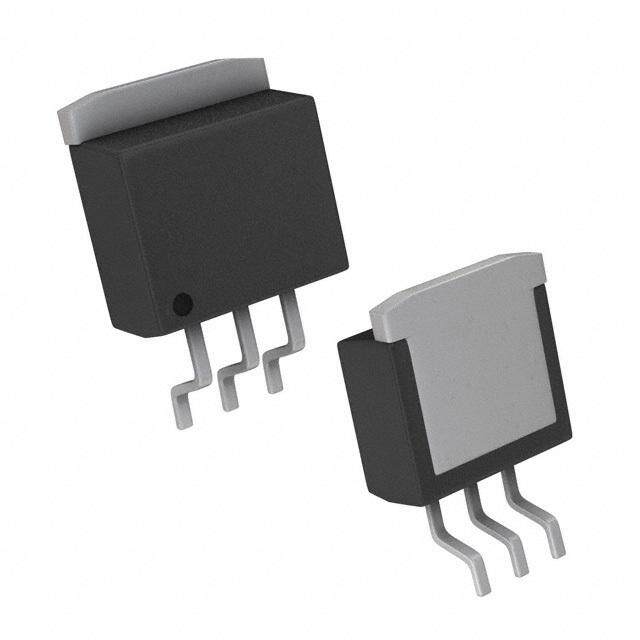
| 描述 | IC REG LDO 3.3V 0.5A TO252-3低压差稳压器 Sgl Out LDO,500mA Fixed,Load Dump Prot |
| 产品分类 | |
| 品牌 | Texas Instruments |
| 产品手册 | |
| 产品图片 |
|
| rohs | 符合RoHS无铅 / 符合限制有害物质指令(RoHS)规范要求 |
| 产品系列 | 电源管理 IC,低压差稳压器,Texas Instruments TL760M33QKVURQ1自动,AEC-Q100 |
| 数据手册 | |
| 产品型号 | TL760M33QKVURQ1 |
| 产品种类 | 低压差稳压器 |
| 供应商器件封装 | TO-252-3 |
| 其它名称 | 296-27620-6 |
| 包装 | Digi-Reel® |
| 单位重量 | 328.800 mg |
| 商标 | Texas Instruments |
| 回动电压—最大值 | 400 mV at 250 mA |
| 安装类型 | 表面贴装 |
| 安装风格 | SMD/SMT |
| 封装 | Reel |
| 封装/外壳 | TO-252-3,DPak(2 引线+接片),SC-63 |
| 封装/箱体 | TO-252-3 |
| 工作温度 | -40°C ~ 125°C |
| 工厂包装数量 | 2500 |
| 最大工作温度 | + 125 C |
| 最大输入电压 | 26 V |
| 最小工作温度 | - 40 C |
| 最小输入电压 | + 3 V |
| 标准包装 | 1 |
| 电压-跌落(典型值) | - |
| 电压-输入 | 最高 26V |
| 电压-输出 | 3.3V |
| 电压调节准确度 | 3 % |
| 电流-输出 | 500mA |
| 电流-限制(最小值) | - |
| 稳压器拓扑 | 正,固定式 |
| 稳压器数 | 1 |
| 系列 | TL760M33-Q1 |
| 线路调整率 | 25 mV |
| 负载调节 | 30 mV |
| 输出电压 | 3.3 V |
| 输出电流 | 500 mA |
| 输出端数量 | 1 Output |
| 输出类型 | Fixed |


- 商务部:美国ITC正式对集成电路等产品启动337调查
- 曝三星4nm工艺存在良率问题 高通将骁龙8 Gen1或转产台积电
- 太阳诱电将投资9.5亿元在常州建新厂生产MLCC 预计2023年完工
- 英特尔发布欧洲新工厂建设计划 深化IDM 2.0 战略
- 台积电先进制程称霸业界 有大客户加持明年业绩稳了
- 达到5530亿美元!SIA预计今年全球半导体销售额将创下新高
- 英特尔拟将自动驾驶子公司Mobileye上市 估值或超500亿美元
- 三星加码芯片和SET,合并消费电子和移动部门,撤换高东真等 CEO
- 三星电子宣布重大人事变动 还合并消费电子和移动部门
- 海关总署:前11个月进口集成电路产品价值2.52万亿元 增长14.8%


PDF Datasheet 数据手册内容提取
TL760M33-Q1 www.ti.com SGLS284I–OCTOBER2005–REVISEDDECEMBER2010 LOW-DROPOUT FIXED-VOLTAGE REGULATORS CheckforSamples:TL760M33-Q1 FEATURES 1 KTT(TO-263)PACKAGE • QualifiedforAutomotiveApplications (TOPVIEW) • ±3%OutputVoltageVariationAcrossLoad OUTPUT andTemperature D • Load-DumpProtection N GND G • 500-mVMaximumDropoutVoltageat500mA INPUT • Fixed3.3-VOutput • InternalThermal-OverloadProtection • InternalOvervoltageProtection KVU (TO-252) PACKAGE (TOPVIEW) • Customer-SpecificConfigurationControlCan OUTPUT BeSupportedAlongWithMajor-Change D Approval N GND G INPUT DESCRIPTION/ORDERING INFORMATION The TL760M33-Q1 low-dropout regulator offers a variety of fixed-voltage options that offer a maximum continuous input voltage of 26 V. Utilizing a pnp pass element, this regulator is capable of sourcing 500 mA of current, with a specified maximum dropout of 500 mV, making the TL760M33-Q1 ideal for low-voltage applications. Additionally, the TL760M33-Q1 regulator offers very tight output accuracy of ±3% across operating load and temperature ranges. Other convenient features the regulators provide are internal overcurrent limiting, thermal-overload protection, and overvoltage protection. The TL760M33-Q1 is load-dump protected to its maximum operating condition of 45 V. Stability has been optimized for typical automotive applications and low-costcapacitors. ORDERINGINFORMATION(1) T V (TYP) PACKAGE(2) ORDERABLEPARTNUMBER TOP-SIDEMARKING A O TO-263–KTT Reelof500 TL760M33QKTTRQ1 TL760M33Q1 –40°Cto125°C 3.3V TO-252–KVU Reelof2500 TL760M33QKVURQ1 760M33Q1 (1) Forthemostcurrentpackageandorderinginformation,seethePackageOptionAddendumattheendofthisdocument,orseetheTI websiteatwww.ti.com. (2) Packagedrawings,thermaldata,andsymbolizationareavailableatwww.ti.com/packaging. 1 Pleasebeawarethatanimportantnoticeconcerningavailability,standardwarranty,anduseincriticalapplicationsofTexas Instrumentssemiconductorproductsanddisclaimerstheretoappearsattheendofthisdatasheet. UNLESS OTHERWISE NOTED this document contains Copyright©2005–2010,TexasInstrumentsIncorporated PRODUCTION DATA information current as of publication date. Products conform to specifications per the terms of Texas Instruments standard warranty. Production processing does not necessarilyincludetestingofallparameters.
TL760M33-Q1 SGLS284I–OCTOBER2005–REVISEDDECEMBER2010 www.ti.com ABSOLUTE MAXIMUM RATINGS(1) overoperatingvirtualjunctiontemperaturerange(unlessotherwisenoted) V Maximuminputvoltage 45V I T Operatingvirtualjunctiontemperature 150°C J T Storagetemperaturerange –65°Cto150°C stg (1) Stressesbeyondthoselistedunderabsolutemaximumratingsmaycausepermanentdamagetothedevice.Thesearestressratings only,andfunctionaloperationofthedeviceattheseoranyotherconditionsbeyondthoseindicatedunderrecommendedoperating conditionsisnotimplied.Exposuretoabsolute-maximum-ratedconditionsforextendedperiodsmayaffectdevicereliability. PACKAGE THERMAL DATA(1) PACKAGE BOARD q JA TO-252(KVU) HighK,JESD51-5 30.3°C/W TO-263(KTT) HighK,JESD51-5 26.9°C/W (1) MaximumpowerdissipationisafunctionofT(max),q ,andT .Themaximumallowablepowerdissipationatanyallowableambient J JA A temperatureisP =(T(max)–T )/q .OperatingattheabsolutemaximumT of150°Ccanimpactreliability. D J A JA J THERMAL RESISTANCE 1-ozcopper,one-layerPCB THERMALRESISTANCE VALUE R 55°C/W(area=240mm2) JA R 5.5°C/WfromFETtotab JC R 0.1°C/Wfromdiecentertotab JC RECOMMENDED OPERATING CONDITIONS MIN MAX UNIT V Inputvoltage 3.8 26 V I I Outputcurrent 0 500 mA O T Operatingvirtual-junctiontemperature –40 150 °C J ELECTRICAL CHARACTERISTICS V =6V,I =500mA,T =–40°Cto150°C(unlessotherwisenoted) I O J PARAMETER TESTCONDITIONS(1) MIN TYP MAX UNIT I =5mAto500mA,V =3.8Vto26V,T =125°C 3.2 3.3 3.4 O I J V Outputvoltage V O T =150°C,I =5mAto300mA,V =3.8Vto26V 3.2 3.3 3.4 J O I I =250mA 8 15 O I Currentconsumption,I =I –I V =6V mA Q Q I O I I =500mA 20 30 O Lineregulation V =3.8Vto28V 10 25 mV I PSRR Power-supplyripplerejection f=100Hz,V =0.5V ,V =6V 62 dB ripple PP I Loadregulation I =5mAto500mA 5 30 mV O I =250mA 400 V Dropoutvoltage(2) O mV DO I =500mA 500 O (1) Pulse-testingtechniquesareusedtomaintainthevirtualjunctiontemperatureasclosetotheambienttemperatureaspossible.Thermal effectsmustbetakenintoaccountseparately.Allcharacteristicsaremeasuredwitha0.1-mFcapacitoracrosstheinputanda22-mF tantalumcapacitor,withequivalentseriesresistanceof1.5Ωontheoutput. (2) Measuredwhentheoutputvoltage,V ,hasdropped100mVfromthenominalvalueobtainedwhenV =6V O I 2 SubmitDocumentationFeedback Copyright©2005–2010,TexasInstrumentsIncorporated
TL760M33-Q1 www.ti.com SGLS284I–OCTOBER2005–REVISEDDECEMBER2010 COMPENSATION-CAPACITOR SELECTION INFORMATION The TL760M is a low-dropout regulator. This means that the capacitance loading is important to the performance of the regulator because it is a vital part of the control loop. The capacitor value and the equivalent series resistance (ESR) both affect the control loop and must be defined for the load range. Figure 1 can be used to establishthecapacitancevalueandESRrangeforthebestregulatorperformance. = 22mF = 0.1mF )W R ( 1000mF S E e, c n a st si 400mF e R s rie 0.015 200mF e S nt e al v ui q 22mF E 10mF Load Current,I (A) L DI L DV L DV = ESRxDI L L Figure1. Figure2. TYPICAL APPLICATION SCHEMATIC 22 Figure3. Copyright©2005–2010,TexasInstrumentsIncorporated SubmitDocumentationFeedback 3
TL760M33-Q1 SGLS284I–OCTOBER2005–REVISEDDECEMBER2010 www.ti.com TYPICAL CHARACTERISTICS Figure4. Figure5. 4 SubmitDocumentationFeedback Copyright©2005–2010,TexasInstrumentsIncorporated
PACKAGE OPTION ADDENDUM www.ti.com 6-Feb-2020 PACKAGING INFORMATION Orderable Device Status Package Type Package Pins Package Eco Plan Lead/Ball Finish MSL Peak Temp Op Temp (°C) Device Marking Samples (1) Drawing Qty (2) (6) (3) (4/5) TL760M33QKTTRQ1 ACTIVE DDPAK/ KTT 3 500 Green (RoHS SN Level-3-245C-168 HR -40 to 125 TL760M33Q1 TO-263 & no Sb/Br) TL760M33QKVURQ1 ACTIVE TO-252 KVU 3 2500 Green (RoHS SN Level-3-260C-168 HR -40 to 125 760M33Q1 & no Sb/Br) (1) The marketing status values are defined as follows: ACTIVE: Product device recommended for new designs. LIFEBUY: TI has announced that the device will be discontinued, and a lifetime-buy period is in effect. NRND: Not recommended for new designs. Device is in production to support existing customers, but TI does not recommend using this part in a new design. PREVIEW: Device has been announced but is not in production. Samples may or may not be available. OBSOLETE: TI has discontinued the production of the device. (2) RoHS: TI defines "RoHS" to mean semiconductor products that are compliant with the current EU RoHS requirements for all 10 RoHS substances, including the requirement that RoHS substance do not exceed 0.1% by weight in homogeneous materials. Where designed to be soldered at high temperatures, "RoHS" products are suitable for use in specified lead-free processes. TI may reference these types of products as "Pb-Free". RoHS Exempt: TI defines "RoHS Exempt" to mean products that contain lead but are compliant with EU RoHS pursuant to a specific EU RoHS exemption. Green: TI defines "Green" to mean the content of Chlorine (Cl) and Bromine (Br) based flame retardants meet JS709B low halogen requirements of <=1000ppm threshold. Antimony trioxide based flame retardants must also meet the <=1000ppm threshold requirement. (3) MSL, Peak Temp. - The Moisture Sensitivity Level rating according to the JEDEC industry standard classifications, and peak solder temperature. (4) There may be additional marking, which relates to the logo, the lot trace code information, or the environmental category on the device. (5) Multiple Device Markings will be inside parentheses. Only one Device Marking contained in parentheses and separated by a "~" will appear on a device. If a line is indented then it is a continuation of the previous line and the two combined represent the entire Device Marking for that device. (6) Lead/Ball Finish - Orderable Devices may have multiple material finish options. Finish options are separated by a vertical ruled line. Lead/Ball Finish values may wrap to two lines if the finish value exceeds the maximum column width. Important Information and Disclaimer:The information provided on this page represents TI's knowledge and belief as of the date that it is provided. TI bases its knowledge and belief on information provided by third parties, and makes no representation or warranty as to the accuracy of such information. Efforts are underway to better integrate information from third parties. TI has taken and continues to take reasonable steps to provide representative and accurate information but may not have conducted destructive testing or chemical analysis on incoming materials and chemicals. TI and TI suppliers consider certain information to be proprietary, and thus CAS numbers and other limited information may not be available for release. In no event shall TI's liability arising out of such information exceed the total purchase price of the TI part(s) at issue in this document sold by TI to Customer on an annual basis. Addendum-Page 1
PACKAGE OPTION ADDENDUM www.ti.com 6-Feb-2020 Addendum-Page 2
PACKAGE MATERIALS INFORMATION www.ti.com 29-May-2013 TAPE AND REEL INFORMATION *Alldimensionsarenominal Device Package Package Pins SPQ Reel Reel A0 B0 K0 P1 W Pin1 Type Drawing Diameter Width (mm) (mm) (mm) (mm) (mm) Quadrant (mm) W1(mm) TL760M33QKVURQ1 TO-252 KVU 3 2500 330.0 16.4 6.9 10.5 2.7 8.0 16.0 Q2 PackMaterials-Page1
PACKAGE MATERIALS INFORMATION www.ti.com 29-May-2013 *Alldimensionsarenominal Device PackageType PackageDrawing Pins SPQ Length(mm) Width(mm) Height(mm) TL760M33QKVURQ1 TO-252 KVU 3 2500 340.0 340.0 38.0 PackMaterials-Page2
None
PACKAGE OUTLINE KVU0003A TO-252 - 2.52 mm max height SCALE 1.500 TO-252 10.41 9.40 6.22 1.27 B A 5.97 0.89 1 2.29 6.70 2 5.460 6.35 4.58 4.953 3 0.890 3X 1.02 0.635 OPTIONAL NOTE 3 0.61 0.25 C A B 0.61 2.52 MAX C 0.46 0.61 0.46 SEE DETAIL A 5.21 MIN 3 4.32 2 4 MIN 1 EXPOSED 0.51 THERMAL PAD GAGE PLANE NOTE 3 0.13 0 -8 1.78 0.00 1.40 DETA 7.000AIL A TYPICAL 4218915/A 02/2017 NOTES: 1. All linear dimensions are in millimeters. Any dimensions in parenthesis are for reference only. Dimensioning and tolerancing per ASME Y14.5M. 2. This drawing is subject to change without notice. 3. Shape may vary per different assembly sites. 4. Reference JEDEC registration TO-252. www.ti.com
EXAMPLE BOARD LAYOUT KVU0003A TO-252 - 2.52 mm max height TO-252 2X (2.75) (6.15) 2X (1) 1 4 SYMM (4.58) (5.55) 3 (R0.05) TYP (4.2) (2.5) PKG LAND PATTERN EXAMPLE EXPOSED METAL SHOWN SCALE:6X 0.07 MAX 0.07 MIN ALL AROUND ALL AROUND EXPOSED METAL EXPOSED METAL SOLDER MASK METAL METAL UNDER SOLDER MASK OPENING SOLDER MASK OPENING NON SOLDER MASK SOLDER MASK DEFINED DEFINED SOLDER MASK DETAILS NOT TO SCALE 4218915/A 02/2017 NOTES: (continued) 5. This package is designed to be soldered to a thermal pad on the board. For more information, see Texas Instruments literature numbers SLMA002(www.ti.com/lit/slm002) and SLMA004 (www.ti.com/lit/slma004). 6. Vias are optional depending on application, refer to device data sheet. It is recommended that vias under paste be filled, plugged or tented. www.ti.com
EXAMPLE STENCIL DESIGN KVU0003A TO-252 - 2.52 mm max height TO-252 (1.18) TYP 2X (2.75) 2X (1) (0.14) 1 (R0.05) (1.33) TYP SYMM (4.58) 4 3 20X (1.13) (4.2) 20X (0.98) PKG SOLDER PASTE EXAMPLE BASED ON 0.125 mm THICK STENCIL EXPOSED PAD 65% PRINTED SOLDER COVERAGE BY AREA SCALE:8X 4218915/A 02/2017 NOTES: (continued) 7. Laser cutting apertures with trapezoidal walls and rounded corners may offer better paste release. IPC-7525 may have alternate design recommendations. 8. Board assembly site may have different recommendations for stencil design. www.ti.com
None
None
IMPORTANTNOTICEANDDISCLAIMER TI PROVIDES TECHNICAL AND RELIABILITY DATA (INCLUDING DATASHEETS), DESIGN RESOURCES (INCLUDING REFERENCE DESIGNS), APPLICATION OR OTHER DESIGN ADVICE, WEB TOOLS, SAFETY INFORMATION, AND OTHER RESOURCES “AS IS” AND WITH ALL FAULTS, AND DISCLAIMS ALL WARRANTIES, EXPRESS AND IMPLIED, INCLUDING WITHOUT LIMITATION ANY IMPLIED WARRANTIES OF MERCHANTABILITY, FITNESS FOR A PARTICULAR PURPOSE OR NON-INFRINGEMENT OF THIRD PARTY INTELLECTUAL PROPERTY RIGHTS. These resources are intended for skilled developers designing with TI products. You are solely responsible for (1) selecting the appropriate TI products for your application, (2) designing, validating and testing your application, and (3) ensuring your application meets applicable standards, and any other safety, security, or other requirements. These resources are subject to change without notice. TI grants you permission to use these resources only for development of an application that uses the TI products described in the resource. Other reproduction and display of these resources is prohibited. No license is granted to any other TI intellectual property right or to any third party intellectual property right. TI disclaims responsibility for, and you will fully indemnify TI and its representatives against, any claims, damages, costs, losses, and liabilities arising out of your use of these resources. TI’s products are provided subject to TI’s Terms of Sale (www.ti.com/legal/termsofsale.html) or other applicable terms available either on ti.com or provided in conjunction with such TI products. TI’s provision of these resources does not expand or otherwise alter TI’s applicable warranties or warranty disclaimers for TI products. Mailing Address: Texas Instruments, Post Office Box 655303, Dallas, Texas 75265 Copyright © 2020, Texas Instruments Incorporated