ICGOO在线商城 > 集成电路(IC) > PMIC - 稳压器 - 线性 > TL750L10CDR

 Datasheet下载
- 型号: TL750L10CDR
- 制造商: Texas Instruments
- 库位|库存: xxxx|xxxx
- 要求:
| 数量阶梯 | 香港交货 | 国内含税 |
| +xxxx | $xxxx | ¥xxxx |
查看当月历史价格
查看今年历史价格
TL750L10CDR产品简介:
ICGOO电子元器件商城为您提供TL750L10CDR由Texas Instruments设计生产,在icgoo商城现货销售,并且可以通过原厂、代理商等渠道进行代购。 TL750L10CDR价格参考¥1.47-¥4.22。Texas InstrumentsTL750L10CDR封装/规格:PMIC - 稳压器 - 线性, Linear Voltage Regulator IC Positive Fixed 1 Output 10V 150mA 8-SOIC。您可以下载TL750L10CDR参考资料、Datasheet数据手册功能说明书,资料中有TL750L10CDR 详细功能的应用电路图电压和使用方法及教程。
Texas Instruments(德州仪器)的TL750L10CDR是一款PMIC(电源管理集成电路)中的线性稳压器。它主要用于为低功耗电子设备提供稳定的电源输出。以下是该型号的应用场景:

1. 便携式电子设备:
   TL750L10CDR适用于便携式设备,如手持终端、遥控器和小型消费电子产品。其低功耗特性和小封装设计使其非常适合对空间和能效要求较高的应用。

2. 嵌入式系统:
   该稳压器可以为各种嵌入式系统供电,例如微控制器单元(MCU)、传感器模块和其他低功耗外围设备。其稳定性和可靠性确保了系统的正常运行。

3. 通信设备:
   在通信领域,TL750L10CDR可用于低功耗的无线模块、蓝牙设备或Zigbee模块中,为射频(RF)电路和信号处理单元提供稳定的电源。

4. 工业控制:
   它适合用于工业自动化设备中的低功耗组件,如数据采集模块、传感器接口和通信接口。其宽输入电压范围和高稳定性使其在工业环境中表现出色。

5. 医疗设备:
   在医疗领域,该器件可用于便携式健康监测设备,如血压计、血糖仪等。其低噪声特性有助于提高测量精度。

6. 电池供电设备:
   TL750L10CDR支持从电池供电的应用场景,例如烟雾报警器、智能手表和物联网(IoT)设备。其高效的电源转换能力延长了电池寿命。

总结来说,TL750L10CDR凭借其低功耗、高稳定性和紧凑的设计,广泛应用于需要高效电源管理的各种电子设备中,特别适合对成本敏感且对性能有一定要求的产品。
| 参数 | 数值 |
| 产品目录 | 集成电路 (IC)半导体 |
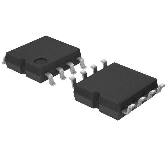
| 描述 | IC REG LDO 10V 0.15A 8SOIC低压差稳压器 Pnp Low Current |
| 产品分类 | |
| 品牌 | Texas Instruments |
| 产品手册 | |
| 产品图片 |
|
| rohs | 符合RoHS无铅 / 符合限制有害物质指令(RoHS)规范要求 |
| 产品系列 | 电源管理 IC,低压差稳压器,Texas Instruments TL750L10CDR- |
| 数据手册 | |
| 产品型号 | TL750L10CDR |
| 产品种类 | 低压差稳压器 |
| 供应商器件封装 | 8-SOIC |
| 其它名称 | 296-31949-2 |
| 包装 | 带卷 (TR) |
| 单位重量 | 72.600 mg |
| 商标 | Texas Instruments |
| 回动电压—最大值 | 200 mV at 10 mA |
| 安装类型 | 表面贴装 |
| 安装风格 | SMD/SMT |
| 封装 | Reel |
| 封装/外壳 | 8-SOIC(0.154",3.90mm 宽) |
| 封装/箱体 | SOIC-8 |
| 工作温度 | 0°C ~ 125°C |
| 工厂包装数量 | 2500 |
| 最大工作温度 | + 125 C |
| 最大输入电压 | 26 V |
| 最小工作温度 | 0 C |
| 最小输入电压 | + 11 V |
| 标准包装 | 2,500 |
| 电压-跌落(典型值) | - |
| 电压-输入 | 11 V ~ 26 V |
| 电压-输出 | 10V |
| 电压调节准确度 | 4 % |
| 电流-输出 | 150mA |
| 电流-限制(最小值) | - |
| 稳压器拓扑 | 正,固定式 |
| 稳压器数 | 1 |
| 系列 | TL750L10 |
| 线路调整率 | 60 mV |
| 负载调节 | 100 mV |
| 输入偏压电流—最大 | 1 mA |
| 输出电压 | 10 V |
| 输出电流 | 150 mA |
| 输出端数量 | 1 Output |
| 输出类型 | Fixed |


- 商务部:美国ITC正式对集成电路等产品启动337调查
- 曝三星4nm工艺存在良率问题 高通将骁龙8 Gen1或转产台积电
- 太阳诱电将投资9.5亿元在常州建新厂生产MLCC 预计2023年完工
- 英特尔发布欧洲新工厂建设计划 深化IDM 2.0 战略
- 台积电先进制程称霸业界 有大客户加持明年业绩稳了
- 达到5530亿美元!SIA预计今年全球半导体销售额将创下新高
- 英特尔拟将自动驾驶子公司Mobileye上市 估值或超500亿美元
- 三星加码芯片和SET,合并消费电子和移动部门,撤换高东真等 CEO
- 三星电子宣布重大人事变动 还合并消费电子和移动部门
- 海关总署:前11个月进口集成电路产品价值2.52万亿元 增长14.8%


PDF Datasheet 数据手册内容提取
TL750L TL751L www.ti.com.................................................................................................................................... SLVS017U–SEPTEMBER1987–REVISEDSEPTEMBER2009 LOW-DROPOUT VOLTAGE REGULATORS FEATURES 1 • VeryLowDropoutVoltage,LessThan0.6Vat • ReverseTransientProtectionDownto–50V 150mA • InternalThermal-OverloadProtection • VeryLowQuiescentCurrent • OvervoltageProtection • TTL-andCMOS-CompatibleEnableonTL751L • InternalOvercurrent-LimitingCircuitry Series • LessThan500-μADisable(TL751LSeries) • 60-VLoad-DumpProtection TL750L...D PACKAGE TL750L...KC PACKAGE TL750L ...KCS PACKAGE (TOPVIEW) (TOPVIEW) (TOPVIEW) N N O OUTPUT O OUTPUT OUTPUT 1 8 INPUT M COMMON M COMMON COMMON 2 7 COMMON OM INPUT OM INPUT COMMON 3 6 COMMON C C NC 4 5 NC NC – No internal connection TL750L...KTE PACKAGE TL750L ...KTT PACKAGE TL750L ...KVU PACKAGE (TOPVIEW) (TOPVIEW) (TOPVIEW) N OUTPUT N OUTPUT N OUTPUT O O O MM COMMON MM COMMON MM COMMON CO INPUT CO INPUT CO INPUT TL750L...LP PACKAGE TL751L...D PACKAGE TL751L ...P PACKAGE (TO-92,TO-226AA) (TOPVIEW) (TOPVIEW) (TOPVIEW) OUTPUT 1 8 INPUT OUTPUT 1 8 INPUT INPUT COMMON 2 7 COMMON NC 2 7 NC COMMON COMMON 3 6 COMMON NC 3 6 COMMON NC 4 5 ENABLE NC 4 5 ENABLE OUTPUT NC – No internal connection NC – No internal connection DESCRIPTION/ORDERING INFORMATION The TL750L and TL751L series of fixed-output voltage regulators offer 5-V, 8-V, 10-V, and 12-V options. The TL751L series also has an enable (ENABLE) input. When ENABLE is high, the regulator output is placed in the high-impedance state. This gives the designer complete control over power up, power down, or emergency shutdown. The TL750L and TL751L series are low-dropout positive-voltage regulators specifically designed for battery-powered systems. These devices incorporate overvoltage and current-limiting protection circuitry, along with internal reverse-battery protection circuitry to protect the devices and the regulated system. The series is fully protected against 60-V load-dump and reverse-battery conditions. Extremely low quiescent current during full-loadconditionsmakesthesedevicesidealforstandbypowersystems. 1 Pleasebeawarethatanimportantnoticeconcerningavailability,standardwarranty,anduseincriticalapplicationsofTexas Instrumentssemiconductorproductsanddisclaimerstheretoappearsattheendofthisdatasheet. PRODUCTIONDATAinformationiscurrentasofpublicationdate. Copyright©1987–2009,TexasInstrumentsIncorporated Products conform to specifications per the terms of the Texas Instruments standard warranty. Production processing does not necessarilyincludetestingofallparameters.
TL750L TL751L SLVS017U–SEPTEMBER1987–REVISEDSEPTEMBER2009.................................................................................................................................... www.ti.com ORDERINGINFORMATION(1) T VOTYP PACKAGE (2) ORDERABLEPARTNUMBER TOP-SIDEMARKING J AT25°C PowerFLEX™–KTE Reelof2000 TL750L05CKTER TL750L05C Tubeof75 TL750L05CD 50L05C Reelof2500 TL750L05CDR SOIC–D Tubeof75 TL751L05CD 51L05C Reelof2500 TL751L05CDR 5V Bulkof1000 TL750L05CLP TO-226/TO-92–LP 750L05C Reelof2000 TL750L05CLPR TO-220–KC Tubeof50 TL750L05CKC TL750L05C TO-220–KCS Tubeof50 TL750L05CKCS TL750L05C TO-252–KVU Reelof2500 TL750L05CKVUR 750L05C TO-263–KTT Reelof500 TL750L05CKTTR 750L05C Tubeof75 TL750L08CD SOIC–D 50L08C 8V Reelof2500 TL750L08CDR 0°Cto125°C TO-226/TO-92–LP Bulkof1000 TL750L08CLP 750L08C PDIP–P Tubeof50 TL751L10CP TL751L10C Tubeof75 TL750L10CD 50L10C Reelof2500 TL750L10CDR SOIC–D 10V Tubeof75 TL751L10CD 51L10C Reelof2500 TL751L10CDR Bulkof1000 TL750L10CLP TO-226/TO-92–LP 750L10C Reelof2000 TL750L10CLPR Tubeof75 TL750L12CD 50L12C Reelof2500 TL750L12CDR SOIC–D 12V Tubeof75 TL751L12CD 51L12C Reelof2500 TL751L12CDR TO-226/TO-92–LP Bulkof1000 TL750L12CLP 750L12C (1) Forthemostcurrentpackageandorderinginformation,seethePackageOptionAddendumattheendofthisdocument,orseetheTI websiteatwww.ti.com. (2) Packagedrawings,thermaldata,andsymbolizationareavailableatwww.ti.com/packaging. DEVICECOMPONENTCOUNT Transistors 20 JFETs 2 Diodes 5 Resistors 16 2 SubmitDocumentationFeedback Copyright©1987–2009,TexasInstrumentsIncorporated
TL750L TL751L www.ti.com.................................................................................................................................... SLVS017U–SEPTEMBER1987–REVISEDSEPTEMBER2009 Absolute Maximum Ratings(1) overoperatingjunctiontemperaturerange(unlessotherwisenoted) MIN MAX UNIT Continuousinputvoltage 26 V Transientinputvoltage(2) T =25°C 60 V A Continuousreverseinputvoltage –15 V Transientreverseinputvoltage t≤100ms –50 V T Operatingvirtualjunctiontemperature 150 °C J Leadtemperature 1,6mm(1/16in)for10s 260 °C T Storagetemperaturerange –65 150 °C stg (1) Stressesbeyondthoselistedunder"absolutemaximumratings"maycausepermanentdamagetothedevice.Thesearestressratings only,andfunctionaloperationofthedeviceattheseoranyotherconditionsbeyondthoseindicatedunder"recommendedoperating conditions"isnotimplied.Exposuretoabsolute-maximum-ratedconditionsforextendedperiodsmayaffectdevicereliability. (2) ThetransientinputvoltageratingappliestothewaveformshowninFigure1. Package Thermal Data(1) PACKAGE BOARD θ θ JC JA PDIP(P) HighK,JESD51-7 57°C/W 85°C/W PowerFLEX™(KTE) HighK,JESD51-5 3°C/W 23°C/W SOIC(D) HighK,JESD51-7 39°C/W 97°C/W TO-226/TO-92(LP) HighK,JESD51-7 55°C/W 140°C/W TO-220(KC) HighK,JESD51-5 3°C/W 19°C/W TO-220(KCS) HighK,JESD51-5 3°C/W 19°C/W TO-252(KVU) HighK,JESD51-5 – 30.3°C/W TO-263(KTT) HighK,JESD51-5 18°C/W 25.3°C/W (1) MaximumpowerdissipationisafunctionofT(max),θ ,andT .Themaximumallowablepowerdissipationatanyallowableambient J JA A temperatureisP =(T(max)–T )/θ .OperatingattheabsolutemaximumT of150°Ccanaffectreliability. D J A JA J Recommended Operating Conditions overrecommendedoperatingjunctiontemperaturerange(unlessotherwisenoted) MIN MAX UNIT TL75xL05 6 26 TL75xL08 9 26 V Inputvoltage V I TL75xL10 11 26 TL75xL12 13 26 V High-levelENABLEinputvoltage TL75xLxx 2 15 V IH T =25°C TL75xLxx –0.3 0.8 V (1) Low-levelENABLEinputvoltage J V IL T =0°Cto125°C TL75xLxx –0.15 0.8 J I Outputcurrent TL75xLxx 0 150 mA O T Operatingvirtualjunctiontemperature TL75xLxxC 0 125 °C J (1) Thealgebraicconvention,inwhichtheleastpositive(mostnegative)valueisdesignatedminimum,isusedinthisdatasheetfor ENABLEvoltagelevelsandtemperatureonly. Copyright©1987–2009,TexasInstrumentsIncorporated SubmitDocumentationFeedback 3
TL750L TL751L SLVS017U–SEPTEMBER1987–REVISEDSEPTEMBER2009.................................................................................................................................... www.ti.com TL75xL05 Electrical Characteristics(1) V =14V,I =10mA,T =25°C(unlessotherwisenoted) I O J TL750L05 PARAMETER TESTCONDITIONS TL751L05 UNIT MIN TYP MAX T =25°C 4.8 5 5.2 J Outputvoltage V =6Vto26V,I =0to150mA V I O T =0°Cto125°C 4.75 5.25 J V =9Vto16V 5 10 I Inputregulationvoltage mV V =6Vto26V 6 30 I Ripplerejection V =8Vto18V,f=120Hz 60 65 dB I Outputregulationvoltage I =5mAto150mA 20 50 mV O I =10mA 0.2 O Dropoutvoltage V I =150mA 0.6 O Outputnoisevoltage f=10Hzto100kHz 500 μV I =150mA 10 12 O Quiescentcurrent V =6Vto26V,I =10mA,T =0°Cto125°C 1 2 mA I O J ENABLE≥2V 0.5 (1) Pulse-testingtechniquesareusedtomaintainthejunctiontemperatureasclosetotheambienttemperatureaspossible.Thermaleffects mustbetakenintoaccountseparately.Allcharacteristicsaremeasuredwitha0.1-μFcapacitoracrosstheinputanda10-μFcapacitor, withequivalentseriesresistanceoflessthan0.4Ω,acrosstheoutput. TL75xL08 Electrical Characteristics(1) V =14V,I =10mA,T =25°C(unlessotherwisenoted) I O J TL750L08 PARAMETER TESTCONDITIONS TL751L08 UNIT MIN TYP MAX T =25°C 7.68 8 8.32 J Outputvoltage V =9Vto26V,I =0to150mA V I O T =0°Cto125°C 7.6 8.4 J V =10Vto17V 10 20 I Inputregulationvoltage mV V =9Vto26V 25 50 I Ripplerejection V =11Vto21V,f=120Hz 60 65 dB I Outputregulationvoltage I =5mAto150mA 40 80 mV O I =10mA 0.2 O Dropoutvoltage V I =150mA 0.6 O Outputnoisevoltage f=10Hzto100kHz 500 μV I =150mA 10 12 O Quiescentcurrent V =9Vto26V,I =10mA,T =0°Cto125°C 1 2 mA I O J ENABLE≥2V 0.5 (1) Pulse-testingtechniquesareusedtomaintainthejunctiontemperatureasclosetotheambienttemperatureaspossible.Thermaleffects mustbetakenintoaccountseparately.Allcharacteristicsaremeasuredwitha0.1-μFcapacitoracrosstheinputanda10-μFcapacitor, withequivalentseriesresistanceoflessthan0.4Ω,acrosstheoutput. 4 SubmitDocumentationFeedback Copyright©1987–2009,TexasInstrumentsIncorporated
TL750L TL751L www.ti.com.................................................................................................................................... SLVS017U–SEPTEMBER1987–REVISEDSEPTEMBER2009 TL75xL10 Electrical Characteristics(1) V =14V,I =10mA,T =25°C(unlessotherwisenoted) I O J TL750L10 PARAMETER TESTCONDITIONS TL751L10 UNIT MIN TYP MAX T =25°C 9.6 10 10.4 J Outputvoltage V =11Vto26V,I =0to150mA V I O T =0°Cto125°C 9.5 10.5 J V =12Vto19V 10 25 I Inputregulationvoltage mV V =11Vto26V 30 60 I Ripplerejection V =12Vto22V,f=120Hz 60 65 dB I Outputregulationvoltage I =5mAto150mA 50 100 mV O I =10mA 0.2 O Dropoutvoltage V I =150mA 0.6 O Outputnoisevoltage f=10Hzto100kHz 700 μV I =150mA 10 12 O Quiescentcurrent V =11Vto26V,I =10mA,T =0°Cto125°C 1 2 mA I O J ENABLE≥2V 0.5 (1) Pulse-testingtechniquesareusedtomaintainthejunctiontemperatureasclosetotheambienttemperatureaspossible.Thermaleffects mustbetakenintoaccountseparately.Allcharacteristicsaremeasuredwitha0.1-μFcapacitoracrosstheinputanda10-μFcapacitor, withequivalentseriesresistanceoflessthan0.4Ω,acrosstheoutput. TL75xL12 Electrical Characteristics(1) V =14V,I =10mA,T =25°C(unlessotherwisenoted) I O J TL750L12 PARAMETER TESTCONDITIONS TL751L12 UNIT MIN TYP MAX T =25°C 11.52 12 12.48 J Outputvoltage V =13Vto26V,I =0to150mA V I O T =0°Cto125°C 11.4 12.6 J V =14Vto19V 15 30 I Inputregulationvoltage mV V =13Vto26V 20 40 I Ripplerejection V =13Vto23V,f=120Hz 50 55 dB I Outputregulationvoltage I =5mAto150mA 50 120 mV O I =10mA 0.2 O Dropoutvoltage V I =150mA 0.6 O Outputnoisevoltage f=10Hzto100kHz 700 μV I =150mA 10 12 O Quiescentcurrent V =13Vto26V,I =10mA,T =0°Cto125°C 1 2 mA I O J ENABLE≥2V 0.5 (1) Pulse-testingtechniquesareusedtomaintainthejunctiontemperatureasclosetotheambienttemperatureaspossible.Thermaleffects mustbetakenintoaccountseparately.Allcharacteristicsaremeasuredwitha0.1-μFcapacitoracrosstheinputanda10-μFcapacitor, withequivalentseriesresistanceoflessthan0.4Ω,acrosstheoutput. PARAMETER MEASUREMENT INFORMATION The TL750L, TL751L series are low-dropout regulators. This means that capacitance loading is important to the performance of the regulator because it is a vital part of the control loop. The capacitor value and its equivalent series resistance (ESR) both affect the control loop and must be defined for the load range and temperature range.Figure1showstherecommendedrangeofESRforagivenloadwitha10-μFcapacitorontheoutput. Copyright©1987–2009,TexasInstrumentsIncorporated SubmitDocumentationFeedback 5
TL750L TL751L SLVS017U–SEPTEMBER1987–REVISEDSEPTEMBER2009.................................................................................................................................... www.ti.com TYPICAL CHARACTERISTICS TL750L05 EQUIVALENTSERIESRESISTANCE TRANSIENTINPUTVOLTAGE vs vs LOADCURRENT TIME 1.0 60 0.9 CTAL == −104-0m°FC Ttoan 1t2a5lu°Cm Capacitor TVAI == 1245 °VC + 46e(−t/0.230) Wnce − 0.8 Potential Instability Region e − V 50 for t ≥ 5 ms sista 0.7 oltag 40 s Re 0.6 ut V ÎÎÎ e p Seri 0.5 nt In 30 ÎÎÎ ent 0.4 sie Îtr =Î 1 mÎs − Equival 00..23 Region of Best Stability V − Trani 20 ÎÎÎ R 10 S E 0.1 0.024 Potential Instability Region 0 0 0 10 80 120 150 0 100 200 300 400 500 600 IL − Load Current − mA t − Time − ms Figure1. Figure2. TL750L05 TL750L12 INPUTCURRENT INPUTCURRENT vs vs INPUTVOLTAGE INPUTVOLTAGE 40 60 35 50 30 A A m 40 m nt − 25 ent − e r rr 20 ur 30 u C put C 15 nput − InII 10 − III 20 10 5 0 0 0 1 2 3 4 5 6 0 2 4 6 8 10 12 14 VI − Input Voltage − V VI − Input Voltage − V Figure3. Figure4. 6 SubmitDocumentationFeedback Copyright©1987–2009,TexasInstrumentsIncorporated
PACKAGE OPTION ADDENDUM www.ti.com 6-Feb-2020 PACKAGING INFORMATION Orderable Device Status Package Type Package Pins Package Eco Plan Lead/Ball Finish MSL Peak Temp Op Temp (°C) Device Marking Samples (1) Drawing Qty (2) (6) (3) (4/5) TL750L05CD ACTIVE SOIC D 8 75 Green (RoHS NIPDAU Level-1-260C-UNLIM 0 to 125 50L05C & no Sb/Br) TL750L05CDR ACTIVE SOIC D 8 2500 Green (RoHS NIPDAU Level-1-260C-UNLIM 0 to 125 50L05C & no Sb/Br) TL750L05CKCS ACTIVE TO-220 KCS 3 50 Pb-Free SN N / A for Pkg Type 0 to 125 TL750L05C (RoHS) TL750L05CKCSE3 ACTIVE TO-220 KCS 3 50 Pb-Free SN N / A for Pkg Type 0 to 125 TL750L05C (RoHS) TL750L05CKTTR ACTIVE DDPAK/ KTT 3 500 Green (RoHS SN Level-3-245C-168 HR 0 to 125 TL750L05C TO-263 & no Sb/Br) TL750L05CKTTRG3 ACTIVE DDPAK/ KTT 3 500 Green (RoHS SN Level-3-245C-168 HR 0 to 125 TL750L05C TO-263 & no Sb/Br) TL750L05CKVURG3 ACTIVE TO-252 KVU 3 2500 Green (RoHS SN Level-3-260C-168 HR 0 to 125 750L05C & no Sb/Br) TL750L05CLP ACTIVE TO-92 LP 3 1000 Pb-Free SN N / A for Pkg Type 0 to 125 750L05C (RoHS) TL750L05CLPE3 ACTIVE TO-92 LP 3 1000 Pb-Free SN N / A for Pkg Type 0 to 125 750L05C (RoHS) TL750L05CLPR ACTIVE TO-92 LP 3 2000 Pb-Free SN N / A for Pkg Type 0 to 125 750L05C (RoHS) TL750L05CLPRE3 ACTIVE TO-92 LP 3 2000 Pb-Free SN N / A for Pkg Type 0 to 125 750L05C (RoHS) TL750L08CD ACTIVE SOIC D 8 75 Green (RoHS NIPDAU Level-2-260C-1 YEAR 0 to 125 50L08C & no Sb/Br) TL750L08CDR ACTIVE SOIC D 8 2500 Green (RoHS NIPDAU Level-2-260C-1 YEAR 0 to 125 50L08C & no Sb/Br) TL750L08CLP ACTIVE TO-92 LP 3 1000 Pb-Free SN N / A for Pkg Type 0 to 125 750L08C (RoHS) TL750L08CLPE3 ACTIVE TO-92 LP 3 1000 Pb-Free SN N / A for Pkg Type 0 to 125 750L08C (RoHS) TL750L10CD ACTIVE SOIC D 8 75 Green (RoHS NIPDAU Level-1-260C-UNLIM 0 to 125 50L10C & no Sb/Br) TL750L10CDR ACTIVE SOIC D 8 2500 Green (RoHS NIPDAU Level-1-260C-UNLIM 0 to 125 50L10C & no Sb/Br) Addendum-Page 1
PACKAGE OPTION ADDENDUM www.ti.com 6-Feb-2020 Orderable Device Status Package Type Package Pins Package Eco Plan Lead/Ball Finish MSL Peak Temp Op Temp (°C) Device Marking Samples (1) Drawing Qty (2) (6) (3) (4/5) TL750L10CLP ACTIVE TO-92 LP 3 1000 Pb-Free SN N / A for Pkg Type 0 to 125 750L10C (RoHS) TL750L10CLPR ACTIVE TO-92 LP 3 2000 Pb-Free SN N / A for Pkg Type 0 to 125 750L10C (RoHS) TL750L12CD ACTIVE SOIC D 8 75 Green (RoHS NIPDAU Level-1-260C-UNLIM 0 to 125 50L12C & no Sb/Br) TL750L12CDR ACTIVE SOIC D 8 2500 Green (RoHS NIPDAU Level-1-260C-UNLIM 0 to 125 50L12C & no Sb/Br) TL750L12CLP ACTIVE TO-92 LP 3 1000 Pb-Free SN N / A for Pkg Type 0 to 125 750L12C (RoHS) TL751L05CD ACTIVE SOIC D 8 75 Green (RoHS NIPDAU Level-1-260C-UNLIM 0 to 125 51L05C & no Sb/Br) TL751L05CDE4 ACTIVE SOIC D 8 75 Green (RoHS NIPDAU Level-1-260C-UNLIM 0 to 125 51L05C & no Sb/Br) TL751L05CDG4 ACTIVE SOIC D 8 75 Green (RoHS NIPDAU Level-1-260C-UNLIM 0 to 125 51L05C & no Sb/Br) TL751L05CDR ACTIVE SOIC D 8 2500 Green (RoHS NIPDAU Level-1-260C-UNLIM 0 to 125 51L05C & no Sb/Br) TL751L10CD ACTIVE SOIC D 8 75 Green (RoHS NIPDAU Level-1-260C-UNLIM 0 to 125 51L10C & no Sb/Br) TL751L10CDR ACTIVE SOIC D 8 2500 Green (RoHS NIPDAU Level-1-260C-UNLIM 0 to 125 51L10C & no Sb/Br) TL751L10CP ACTIVE PDIP P 8 50 Green (RoHS NIPDAU N / A for Pkg Type 0 to 125 TL751L10C & no Sb/Br) TL751L12CD ACTIVE SOIC D 8 75 Green (RoHS NIPDAU Level-1-260C-UNLIM 0 to 125 51L12C & no Sb/Br) TL751L12CDR ACTIVE SOIC D 8 2500 Green (RoHS NIPDAU Level-1-260C-UNLIM 0 to 125 51L12C & no Sb/Br) TL751L12CDRG4 ACTIVE SOIC D 8 2500 Green (RoHS NIPDAU Level-1-260C-UNLIM 0 to 125 51L12C & no Sb/Br) (1) The marketing status values are defined as follows: ACTIVE: Product device recommended for new designs. LIFEBUY: TI has announced that the device will be discontinued, and a lifetime-buy period is in effect. NRND: Not recommended for new designs. Device is in production to support existing customers, but TI does not recommend using this part in a new design. PREVIEW: Device has been announced but is not in production. Samples may or may not be available. OBSOLETE: TI has discontinued the production of the device. Addendum-Page 2
PACKAGE OPTION ADDENDUM www.ti.com 6-Feb-2020 (2) RoHS: TI defines "RoHS" to mean semiconductor products that are compliant with the current EU RoHS requirements for all 10 RoHS substances, including the requirement that RoHS substance do not exceed 0.1% by weight in homogeneous materials. Where designed to be soldered at high temperatures, "RoHS" products are suitable for use in specified lead-free processes. TI may reference these types of products as "Pb-Free". RoHS Exempt: TI defines "RoHS Exempt" to mean products that contain lead but are compliant with EU RoHS pursuant to a specific EU RoHS exemption. Green: TI defines "Green" to mean the content of Chlorine (Cl) and Bromine (Br) based flame retardants meet JS709B low halogen requirements of <=1000ppm threshold. Antimony trioxide based flame retardants must also meet the <=1000ppm threshold requirement. (3) MSL, Peak Temp. - The Moisture Sensitivity Level rating according to the JEDEC industry standard classifications, and peak solder temperature. (4) There may be additional marking, which relates to the logo, the lot trace code information, or the environmental category on the device. (5) Multiple Device Markings will be inside parentheses. Only one Device Marking contained in parentheses and separated by a "~" will appear on a device. If a line is indented then it is a continuation of the previous line and the two combined represent the entire Device Marking for that device. (6) Lead/Ball Finish - Orderable Devices may have multiple material finish options. Finish options are separated by a vertical ruled line. Lead/Ball Finish values may wrap to two lines if the finish value exceeds the maximum column width. Important Information and Disclaimer:The information provided on this page represents TI's knowledge and belief as of the date that it is provided. TI bases its knowledge and belief on information provided by third parties, and makes no representation or warranty as to the accuracy of such information. Efforts are underway to better integrate information from third parties. TI has taken and continues to take reasonable steps to provide representative and accurate information but may not have conducted destructive testing or chemical analysis on incoming materials and chemicals. TI and TI suppliers consider certain information to be proprietary, and thus CAS numbers and other limited information may not be available for release. In no event shall TI's liability arising out of such information exceed the total purchase price of the TI part(s) at issue in this document sold by TI to Customer on an annual basis. Addendum-Page 3
PACKAGE MATERIALS INFORMATION www.ti.com 18-Jul-2017 TAPE AND REEL INFORMATION *Alldimensionsarenominal Device Package Package Pins SPQ Reel Reel A0 B0 K0 P1 W Pin1 Type Drawing Diameter Width (mm) (mm) (mm) (mm) (mm) Quadrant (mm) W1(mm) TL750L05CDR SOIC D 8 2500 330.0 12.4 6.4 5.2 2.1 8.0 12.0 Q1 TL750L05CKTTR DDPAK/ KTT 3 500 330.0 24.4 10.8 16.1 4.9 16.0 24.0 Q2 TO-263 TL750L05CKTTR DDPAK/ KTT 3 500 330.0 24.4 10.8 16.3 5.11 16.0 24.0 Q2 TO-263 TL750L05CKVURG3 TO-252 KVU 3 2500 330.0 16.4 6.9 10.5 2.7 8.0 16.0 Q2 TL750L08CDR SOIC D 8 2500 330.0 12.4 6.4 5.2 2.1 8.0 12.0 Q1 TL750L10CDR SOIC D 8 2500 330.0 12.4 6.4 5.2 2.1 8.0 12.0 Q1 TL750L12CDR SOIC D 8 2500 330.0 12.4 6.4 5.2 2.1 8.0 12.0 Q1 TL751L05CDR SOIC D 8 2500 330.0 12.4 6.4 5.2 2.1 8.0 12.0 Q1 TL751L10CDR SOIC D 8 2500 330.0 12.4 6.4 5.2 2.1 8.0 12.0 Q1 TL751L12CDR SOIC D 8 2500 330.0 12.4 6.4 5.2 2.1 8.0 12.0 Q1 PackMaterials-Page1
PACKAGE MATERIALS INFORMATION www.ti.com 18-Jul-2017 *Alldimensionsarenominal Device PackageType PackageDrawing Pins SPQ Length(mm) Width(mm) Height(mm) TL750L05CDR SOIC D 8 2500 340.5 338.1 20.6 TL750L05CKTTR DDPAK/TO-263 KTT 3 500 350.0 334.0 47.0 TL750L05CKTTR DDPAK/TO-263 KTT 3 500 340.0 340.0 38.0 TL750L05CKVURG3 TO-252 KVU 3 2500 340.0 340.0 38.0 TL750L08CDR SOIC D 8 2500 340.5 338.1 20.6 TL750L10CDR SOIC D 8 2500 340.5 338.1 20.6 TL750L12CDR SOIC D 8 2500 340.5 338.1 20.6 TL751L05CDR SOIC D 8 2500 340.5 338.1 20.6 TL751L10CDR SOIC D 8 2500 340.5 338.1 20.6 TL751L12CDR SOIC D 8 2500 340.5 338.1 20.6 PackMaterials-Page2
None
PACKAGE OUTLINE KVU0003A TO-252 - 2.52 mm max height SCALE 1.500 TO-252 10.41 9.40 6.22 1.27 B A 5.97 0.89 1 2.29 6.70 2 5.460 6.35 4.58 4.953 3 0.890 3X 1.02 0.635 OPTIONAL NOTE 3 0.61 0.25 C A B 0.61 2.52 MAX C 0.46 0.61 0.46 SEE DETAIL A 5.21 MIN 3 4.32 2 4 MIN 1 EXPOSED 0.51 THERMAL PAD GAGE PLANE NOTE 3 0.13 0 -8 1.78 0.00 1.40 DETA 7.000AIL A TYPICAL 4218915/A 02/2017 NOTES: 1. All linear dimensions are in millimeters. Any dimensions in parenthesis are for reference only. Dimensioning and tolerancing per ASME Y14.5M. 2. This drawing is subject to change without notice. 3. Shape may vary per different assembly sites. 4. Reference JEDEC registration TO-252. www.ti.com
EXAMPLE BOARD LAYOUT KVU0003A TO-252 - 2.52 mm max height TO-252 2X (2.75) (6.15) 2X (1) 1 4 SYMM (4.58) (5.55) 3 (R0.05) TYP (4.2) (2.5) PKG LAND PATTERN EXAMPLE EXPOSED METAL SHOWN SCALE:6X 0.07 MAX 0.07 MIN ALL AROUND ALL AROUND EXPOSED METAL EXPOSED METAL SOLDER MASK METAL METAL UNDER SOLDER MASK OPENING SOLDER MASK OPENING NON SOLDER MASK SOLDER MASK DEFINED DEFINED SOLDER MASK DETAILS NOT TO SCALE 4218915/A 02/2017 NOTES: (continued) 5. This package is designed to be soldered to a thermal pad on the board. For more information, see Texas Instruments literature numbers SLMA002(www.ti.com/lit/slm002) and SLMA004 (www.ti.com/lit/slma004). 6. Vias are optional depending on application, refer to device data sheet. It is recommended that vias under paste be filled, plugged or tented. www.ti.com
EXAMPLE STENCIL DESIGN KVU0003A TO-252 - 2.52 mm max height TO-252 (1.18) TYP 2X (2.75) 2X (1) (0.14) 1 (R0.05) (1.33) TYP SYMM (4.58) 4 3 20X (1.13) (4.2) 20X (0.98) PKG SOLDER PASTE EXAMPLE BASED ON 0.125 mm THICK STENCIL EXPOSED PAD 65% PRINTED SOLDER COVERAGE BY AREA SCALE:8X 4218915/A 02/2017 NOTES: (continued) 7. Laser cutting apertures with trapezoidal walls and rounded corners may offer better paste release. IPC-7525 may have alternate design recommendations. 8. Board assembly site may have different recommendations for stencil design. www.ti.com
None
None
PACKAGE OUTLINE D0008A SOIC - 1.75 mm max height SCALE 2.800 SMALL OUTLINE INTEGRATED CIRCUIT C SEATING PLANE .228-.244 TYP [5.80-6.19] .004 [0.1] C A PIN 1 ID AREA 6X .050 [1.27] 8 1 2X .189-.197 [4.81-5.00] .150 NOTE 3 [3.81] 4X (0 -15 ) 4 5 8X .012-.020 B .150-.157 [0.31-0.51] .069 MAX [3.81-3.98] .010 [0.25] C A B [1.75] NOTE 4 .005-.010 TYP [0.13-0.25] 4X (0 -15 ) SEE DETAIL A .010 [0.25] .004-.010 0 - 8 [0.11-0.25] .016-.050 [0.41-1.27] DETAIL A (.041) TYPICAL [1.04] 4214825/C 02/2019 NOTES: 1. Linear dimensions are in inches [millimeters]. Dimensions in parenthesis are for reference only. Controlling dimensions are in inches. Dimensioning and tolerancing per ASME Y14.5M. 2. This drawing is subject to change without notice. 3. This dimension does not include mold flash, protrusions, or gate burrs. Mold flash, protrusions, or gate burrs shall not exceed .006 [0.15] per side. 4. This dimension does not include interlead flash. 5. Reference JEDEC registration MS-012, variation AA. www.ti.com
EXAMPLE BOARD LAYOUT D0008A SOIC - 1.75 mm max height SMALL OUTLINE INTEGRATED CIRCUIT 8X (.061 ) [1.55] SYMM SEE DETAILS 1 8 8X (.024) [0.6] SYMM (R.002 ) TYP [0.05] 5 4 6X (.050 ) [1.27] (.213) [5.4] LAND PATTERN EXAMPLE EXPOSED METAL SHOWN SCALE:8X SOLDER MASK SOLDER MASK METAL OPENING OPENING METAL UNDER SOLDER MASK EXPOSED METAL EXPOSED METAL .0028 MAX .0028 MIN [0.07] [0.07] ALL AROUND ALL AROUND NON SOLDER MASK SOLDER MASK DEFINED DEFINED SOLDER MASK DETAILS 4214825/C 02/2019 NOTES: (continued) 6. Publication IPC-7351 may have alternate designs. 7. Solder mask tolerances between and around signal pads can vary based on board fabrication site. www.ti.com
EXAMPLE STENCIL DESIGN D0008A SOIC - 1.75 mm max height SMALL OUTLINE INTEGRATED CIRCUIT 8X (.061 ) [1.55] SYMM 1 8 8X (.024) [0.6] SYMM (R.002 ) TYP [0.05] 5 4 6X (.050 ) [1.27] (.213) [5.4] SOLDER PASTE EXAMPLE BASED ON .005 INCH [0.125 MM] THICK STENCIL SCALE:8X 4214825/C 02/2019 NOTES: (continued) 8. Laser cutting apertures with trapezoidal walls and rounded corners may offer better paste release. IPC-7525 may have alternate design recommendations. 9. Board assembly site may have different recommendations for stencil design. www.ti.com
None
PACKAGE OUTLINE KCS0003B TO-220 - 19.65 mm max height SCALE 0.850 TO-220 4.7 4.4 10.36 1.32 2.9 8.55 9.96 1.22 2.6 8.15 6.5 (6.3) 6.1 ( 3.84) 12.5 12.1 19.65 MAX 9.25 9.05 3X 3.9 MAX 13.12 12.70 1 3 0.90 0.47 3X 0.77 0.34 2.79 2X 2.54 2.59 1.36 3X 1.23 5.08 4222214/B 08/2018 NOTES: 1. Dimensions are in millimeters. Any dimension in brackets or parenthesis are for reference only. Dimensioning and tolerancing per ASME Y14.5M. 2. This drawing is subject to change without notice. 3. Reference JEDEC registration TO-220. www.ti.com
EXAMPLE BOARD LAYOUT KCS0003B TO-220 - 19.65 mm max height TO-220 0.07 MAX 2X (1.7) ALL AROUND 3X (1.2) METAL 2X SOLDER MASK OPENING (1.7) 1 2 3 0.07 MAX R (0.05) ALL AROUND (2.54) SOLDER MASK (5.08) OPENING LAND PATTERN EXAMPLE NON-SOLDER MASK DEFINED SCALE:15X 4222214/B 08/2018 www.ti.com
None
PACKAGE OUTLINE LP0003A TO-92 - 5.34 mm max height SCALE 1.200 SCALE 1.200 TO-92 5.21 4.44 EJECTOR PIN OPTIONAL 5.34 4.32 (1.5) TYP (2.54) SEATING 2X NOTE 3 PLANE 4 MAX (0.51) TYP 6X 0.076 MAX SEATING PLANE 3X 12.7 MIN 0.43 2X 0.55 3X 3X 0.35 2.6 0.2 0.38 2X 1.27 0.13 FORMED LEAD OPTION OTHER DIMENSIONS IDENTICAL STRAIGHT LEAD OPTION TO STRAIGHT LEAD OPTION 2.67 3X 2.03 4.19 3.17 3 2 1 3.43 MIN 4215214/B 04/2017 NOTES: 1. All linear dimensions are in millimeters. Any dimensions in parenthesis are for reference only. Dimensioning and tolerancing per ASME Y14.5M. 2. This drawing is subject to change without notice. 3. Lead dimensions are not controlled within this area. 4. Reference JEDEC TO-226, variation AA. 5. Shipping method: a. Straight lead option available in bulk pack only. b. Formed lead option available in tape and reel or ammo pack. c. Specific products can be offered in limited combinations of shipping medium and lead options. d. Consult product folder for more information on available options. www.ti.com
EXAMPLE BOARD LAYOUT LP0003A TO-92 - 5.34 mm max height TO-92 FULL R TYP 0.05 MAX (1.07) ALL AROUND METAL 3X ( 0.85) HOLE TYP TYP 2X METAL (1.5) 2X (1.5) 2X SOLDER MASK OPENING 1 2 3 (R0.05) TYP 2X (1.07) (1.27) SOLDER MASK (2.54) OPENING LAND PATTERN EXAMPLE STRAIGHT LEAD OPTION NON-SOLDER MASK DEFINED SCALE:15X 0.05 MAX ( 1.4) 2X ( 1.4) ALL AROUND METAL TYP 3X ( 0.9) HOLE METAL 2X (R0.05) TYP 1 2 3 SOLDER MASK OPENING (2.6) SOLDER MASK OPENING (5.2) LAND PATTERN EXAMPLE FORMED LEAD OPTION NON-SOLDER MASK DEFINED SCALE:15X 4215214/B 04/2017 www.ti.com
TAPE SPECIFICATIONS LP0003A TO-92 - 5.34 mm max height TO-92 13.7 11.7 32 23 (2.5) TYP 0.5 MIN 16.5 15.5 11.0 9.75 8.5 8.50 19.0 17.5 2.9 6.75 3.7-4.3 TYP TYP 2.4 5.95 13.0 12.4 FOR FORMED LEAD OPTION PACKAGE 4215214/B 04/2017 www.ti.com
IMPORTANTNOTICEANDDISCLAIMER TI PROVIDES TECHNICAL AND RELIABILITY DATA (INCLUDING DATASHEETS), DESIGN RESOURCES (INCLUDING REFERENCE DESIGNS), APPLICATION OR OTHER DESIGN ADVICE, WEB TOOLS, SAFETY INFORMATION, AND OTHER RESOURCES “AS IS” AND WITH ALL FAULTS, AND DISCLAIMS ALL WARRANTIES, EXPRESS AND IMPLIED, INCLUDING WITHOUT LIMITATION ANY IMPLIED WARRANTIES OF MERCHANTABILITY, FITNESS FOR A PARTICULAR PURPOSE OR NON-INFRINGEMENT OF THIRD PARTY INTELLECTUAL PROPERTY RIGHTS. These resources are intended for skilled developers designing with TI products. You are solely responsible for (1) selecting the appropriate TI products for your application, (2) designing, validating and testing your application, and (3) ensuring your application meets applicable standards, and any other safety, security, or other requirements. These resources are subject to change without notice. TI grants you permission to use these resources only for development of an application that uses the TI products described in the resource. Other reproduction and display of these resources is prohibited. No license is granted to any other TI intellectual property right or to any third party intellectual property right. TI disclaims responsibility for, and you will fully indemnify TI and its representatives against, any claims, damages, costs, losses, and liabilities arising out of your use of these resources. TI’s products are provided subject to TI’s Terms of Sale (www.ti.com/legal/termsofsale.html) or other applicable terms available either on ti.com or provided in conjunction with such TI products. TI’s provision of these resources does not expand or otherwise alter TI’s applicable warranties or warranty disclaimers for TI products. Mailing Address: Texas Instruments, Post Office Box 655303, Dallas, Texas 75265 Copyright © 2020, Texas Instruments Incorporated