ICGOO在线商城 > 集成电路(IC) > PMIC - 电压基准 > TL1431IYDT

 Datasheet下载
- 型号: TL1431IYDT
- 制造商: STMicroelectronics
- 库位|库存: xxxx|xxxx
- 要求:
| 数量阶梯 | 香港交货 | 国内含税 |
| +xxxx | $xxxx | ¥xxxx |
查看当月历史价格
查看今年历史价格
TL1431IYDT产品简介:
ICGOO电子元器件商城为您提供TL1431IYDT由STMicroelectronics设计生产,在icgoo商城现货销售,并且可以通过原厂、代理商等渠道进行代购。 TL1431IYDT价格参考¥2.43-¥2.43。STMicroelectronicsTL1431IYDT封装/规格:PMIC - 电压基准, 分流器 电压基准 IC 36V ±0.4% 100mA 8-SO。您可以下载TL1431IYDT参考资料、Datasheet数据手册功能说明书,资料中有TL1431IYDT 详细功能的应用电路图电压和使用方法及教程。
TL1431IYDT 是意法半导体(STMicroelectronics)生产的一款三端可调电压基准芯片,常用于各类电子设备中提供精确、稳定的参考电压。其应用场景主要包括以下几个方面:

1. 开关电源(SMPS)反馈控制:在DC-DC转换器、AC-DC电源适配器等开关电源设计中,TL1431IYDT用于监测输出电压并提供反馈信号,以维持输出电压的稳定。

2. 电池充电管理电路:在锂电池、镍氢电池等充电器电路中,作为电压检测和控制基准,确保充电过程的安全性和稳定性。

3. 电压监测与比较电路:用于电源监控系统中,当电压超出设定阈值时触发保护机制,如关闭系统或发出警报。

4. 工业控制系统:在工业自动化设备、传感器模块中提供高精度参考电压,确保测量和控制的准确性。

5. 通信设备电源管理:在路由器、交换机、基站等通信设备中,用于电源模块的稳压控制和参考源。

6. 消费类电子产品:如电视、音响、数码相机等产品中的电源部分,用于提升电源效率和稳定性。

TL1431IYDT具有封装小巧、温度稳定性好、动态响应快等特点,适用于需要高精度电压基准的各种中低功率应用场合。
| 参数 | 数值 |
| 产品目录 | 集成电路 (IC) |
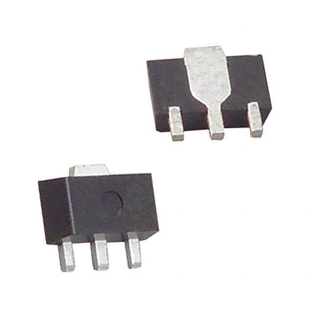
| 描述 | IC VREF SHUNT ADJ 8-SO |
| 产品分类 | |
| 品牌 | STMicroelectronics |
| 数据手册 | |
| 产品图片 |
|
| 产品型号 | TL1431IYDT |
| rohs | 无铅 / 符合限制有害物质指令(RoHS)规范要求 |
| 产品系列 | Q 汽车 |
| 产品目录页面 | |
| 供应商器件封装 | 8-SO |
| 其它名称 | 497-10233-1 |
| 其它有关文件 | http://www.st.com/web/catalog/sense_power/FM1963/SC1771/SS1408/PF65360?referrer=70071840 |
| 包装 | 带卷 (TR) |
| 参考类型 | 分流器,可调式 |
| 安装类型 | 表面贴装 |
| 容差 | ±0.4% |
| 封装/外壳 | 8-SOIC(0.154",3.90mm 宽) |
| 工作温度 | -40°C ~ 125°C |
| 标准包装 | 1 |
| 温度系数 | 100ppm/°C |
| 电压-输入 | - |
| 电压-输出 | 2.5 V ~ 36 V |
| 电流-输出 | 100mA |
| 电流-阴极 | 1mA |
| 电流-静态 | - |
| 通道数 | 1 |


- 商务部:美国ITC正式对集成电路等产品启动337调查
- 曝三星4nm工艺存在良率问题 高通将骁龙8 Gen1或转产台积电
- 太阳诱电将投资9.5亿元在常州建新厂生产MLCC 预计2023年完工
- 英特尔发布欧洲新工厂建设计划 深化IDM 2.0 战略
- 台积电先进制程称霸业界 有大客户加持明年业绩稳了
- 达到5530亿美元!SIA预计今年全球半导体销售额将创下新高
- 英特尔拟将自动驾驶子公司Mobileye上市 估值或超500亿美元
- 三星加码芯片和SET,合并消费电子和移动部门,撤换高东真等 CEO
- 三星电子宣布重大人事变动 还合并消费电子和移动部门
- 海关总署:前11个月进口集成电路产品价值2.52万亿元 增长14.8%


PDF Datasheet 数据手册内容提取
TL1431 Adjustable voltage reference Datasheet - production data Features Adjustable output voltage: V to 36 V REF Sink current capability: 1 to 100 mA Typical output impedance: 0.22 Ω L 0.4% and 0.25% voltage precision SOT23-3L Z Automotive temp. range - 40 °C to +125 °C TO-92 Description (Plastic package) The TL1431 is an adjustable shunt voltage reference with guaranteed temperature stability over the entire operating temperature range. C The output voltage may be set to any value SOT323-6L between 2.5 V and 36 V with two external L resistors. SOT23-5L The TL1431 operates with a wide current range from 1 to 100 mA with a typical dynamic impedance of 0.2 Ω D SO-8 (Batwing plastic micropackage) December 2017 DocID5286 Rev 9 1/27 This is information on a product in full production. www.st.com
Contents TL1431 Contents 1 Schematic diagrams . . . . . . . . . . . . . . . . . . . . . . . . . . . . . . . . . . . . . . . . . 3 2 Absolute maximum ratings and operating conditions . . . . . . . . . . . . . 4 3 Electrical characteristics . . . . . . . . . . . . . . . . . . . . . . . . . . . . . . . . . . . . . 6 4 Parameter definitions . . . . . . . . . . . . . . . . . . . . . . . . . . . . . . . . . . . . . . . 12 4.1 Reference input voltage deviation overtemperature range . . . . . . . . . . . 12 4.2 Temperature coefficient of reference input voltage . . . . . . . . . . . . . . . . . 12 4.3 Dynamic impedance . . . . . . . . . . . . . . . . . . . . . . . . . . . . . . . . . . . . . . . . . 12 5 Package information . . . . . . . . . . . . . . . . . . . . . . . . . . . . . . . . . . . . . . . . 13 5.1 SO-8 package information . . . . . . . . . . . . . . . . . . . . . . . . . . . . . . . . . . . . 14 5.2 TO-92 Ammopack package information . . . . . . . . . . . . . . . . . . . . . . . . . . 15 5.3 TO-92 (bulk) package information . . . . . . . . . . . . . . . . . . . . . . . . . . . . . . 17 5.4 SOT23-3L package information . . . . . . . . . . . . . . . . . . . . . . . . . . . . . . . . 18 5.5 SOT23-5L package information . . . . . . . . . . . . . . . . . . . . . . . . . . . . . . . . 19 5.6 SOT323-6L package information . . . . . . . . . . . . . . . . . . . . . . . . . . . . . . . 20 5.7 SO-8 packing information . . . . . . . . . . . . . . . . . . . . . . . . . . . . . . . . . . . . . 21 5.8 SOT23-3L packing information . . . . . . . . . . . . . . . . . . . . . . . . . . . . . . . . . 22 5.9 SOT23-5L packing information . . . . . . . . . . . . . . . . . . . . . . . . . . . . . . . . . 23 5.10 SOT323-6L packing information . . . . . . . . . . . . . . . . . . . . . . . . . . . . . . . . 24 6 Ordering information . . . . . . . . . . . . . . . . . . . . . . . . . . . . . . . . . . . . . . . 25 7 Revision history . . . . . . . . . . . . . . . . . . . . . . . . . . . . . . . . . . . . . . . . . . . 26 2/27 DocID5286 Rev 9
TL1431 Schematic diagrams 1 Schematic diagrams Figure 1. TO-92 pin connections (top view) Figure 2. SO-8 batwing pin connections (top view) SO8 Cathode 1 8 Ref Anode 2 7 Anode 3 6 NC 4 5 NC Figure 3. SOT23-5L and SOT23-3L pin connections (top view) SOT23-5 SOT23-3 NC 1 5 Anode Cathode 1 NC 2 Cathode 3 4 Ref Ref 2 3 Anode Figure 4. SOT323-6L pin connections (top view) Figure 5. Block diagram Cathode Ref Vref Anode DocID5286 Rev 9 3/27 27
Absolute maximum ratings and operating conditions TL1431 2 Absolute maximum ratings and operating conditions Table 1. Absolute maximum ratings Symbol Parameter Value Unit V Cathode-to-anode voltage 37 V KA Continuous cathode current I -100 to +150 mA k range I Reference input current range -0.05 to +10 mA ref T Junction temperature +150 °C j Power dissipation(1) TO92 625 SO-8 batwing 960 P mW d SOT23-3L 500 SOT23-5L 790 SOT323-6L 565 T Storage temperature range -65 to +150 °C stg HBM: human body model(2) 2000 ESD MM: machine model(3) 200 V CDM: charged device model(4) 1500 1. Calculated with T =+150 °C and T =+25 °C with relative R depending on the package. j amb thja 2. Human body model: A 100pF capacitor is charged to the specified voltage, then discharged through a 1.5kΩresistor between two pins of the device. This happens for all couples of connected pin combinations while the other pins are left floating. 3. Machine model: A 200pF capacitor is charged to the specified voltage, then discharged directly between two pins of the device with no external series resistor (internal resistor < 5Ω). This happens for all couples of connected pin combinations while the other pins are left floating. 4. Charged device model: all pins and the package are charged together to the specified voltage and then discharged directly to the ground through only one pin. This happens for all pins Table 2. Operating conditions Symbol Parameter Value Unit V Cathode-to-anode voltage V to 36 V KA ref I Cathode current 1 to 100 mA k Operating free-air temperature range TL1431C/AC -20 to +70 T °C oper TL1431I/AI -40 to +105 TL1431IY/AIY -40 to +125 4/27 DocID5286 Rev 9
TL1431 Absolute maximum ratings and operating conditions Table 3. Thermal data SO-8 Symbol Parameter TO-92 SOT23-3L SOT23-5L SOT323-6L Unit batwing Thermal R resistance 57 30 136 67 110 thJC junction-case °C/W Thermal R resistance 200 85 248 157 221 thJA junction-ambient DocID5286 Rev 9 5/27 27
Electrical characteristics TL1431 3 Electrical characteristics T = 25 °C (unless otherwise specified). amb Table 4. Electrical characteristics for TL1431C, TL1431AC TL1431C TL1431AC Symbol Parameter Unit Min. Typ. Max. Min. Typ. Max. Reference input voltage - see Figure6 V 2.490 2.500 2.510 2.493 2.500 2.507 V ref V = V , I = 10 mA KA ref k Reference input voltage deviation over temperature range (1) - see Figure6 V 3 20 3 20 mV ref V = V , I = 10 mA, T T KA ref k min amb T max Temperature coefficient of reference -----V----r--e-----f input voltage(2) T ±13 ±90 ±13 ±90 ppm/°C V = V , I = 10 mA, T T KA ref k min amb T max Ratio of change in reference input Vref ---------------- voltage to change in cathode to anode Vka voltage (see Figure7) -2 -1.1 -2 -1.1 mV/V I = 10 mA - V = 36 V to 3 V k KA Reference input current I I = 10 mA, R1 = 10 kΩ, R2 = 1.5 2.5 1.5 2.5 µA ref k T T T 3 3 min amb max Reference input current deviation over temperature range I 0.2 1.2 0.2 1.2 µA ref I = 10 mA, R1 = 10 kΩ, R2 =, T k min T T amb max Minimum cathode current for regulation I Figure6 0.5 1 0.5 0.6 mA min V = V KA ref I Off-state cathode current (see Figure8) 180 500 180 500 nA off Dynamic impedance (3) Z 0.2 0.5 0.2 0.5 Ω KA V = V , I = 1 to100 mA, f 1 kHz KA ref k 1. See Reference input voltage deviation overtemperature range in Section4: Parameter definitions on page12. 2. See Temperature coefficient of reference input voltage in Section4: Parameter definitions on page12. 3. See Dynamic impedance in Section4: Parameter definitions on page12. 6/27 DocID5286 Rev 9
TL1431 Electrical characteristics T = 25 °C (unless otherwise specified). amb Table 5. Electrical characteristics for TL1431I, TL1431AI TL1431I TL1431AI Symbol Parameter Unit Min. Typ. Max. Min. Typ. Max. Reference input voltage - see Figure6 V 2.490 2.500 2.510 2.493 2.500 2.507 V ref V = V , I = 10 mA KA ref k Reference input voltage deviation over V temperature range (1) - see Figure6 7 30 7 30 mV ref V = V , I = 10 mA, T T T KA ref k min amb max Vref Temperature coefficient of reference input ---------T------- voltage(2) ±22 ±100 ±22 ±100 ppm/°C V = V , I = 10 mA, T T T KA ref k min amb max Ratio of change in reference input voltage to Vref ---------------- change in cathode to anode voltage - see Vka Figure7 -2 -1.1 -2 -1.1 mV/V I = 10 mA - V = 36 V to 3 V k KA Reference input current I I = 10 mA, R1 = 10 kΩ, R2 = 1.5 2.5 1.5 2.5 µA ref k T T T 3 3 min amb max Reference input current deviation over temperature range I 0.5 1 0.8 1.2 µA ref I = 10 mA, R1 = 10 kΩ, R2 =, T T k min amb T max Minimum cathode current for regulation - see I Figure6 0.5 1 0.5 0.7 mA min V = V KA ref I Off-state cathode current - see Figure8 180 500 180 500 nA off Dynamic impedance (3) Z 0.2 0.5 0.2 0.5 Ω KA V = V , I = 1 to100 mA, f 1 kHz KA ref k 1. See Reference input voltage deviation overtemperature range in Section4: Parameter definitions on page12. 2. See Temperature coefficient of reference input voltage in Section4: Parameter definitions on page12. 3. See Dynamic impedance in Section4: Parameter definitions on page12. DocID5286 Rev 9 7/27 27
Electrical characteristics TL1431 T = 25 °C (unless otherwise specified). amb Table 6. Electrical characteristics for TL1431IY, TL1431AIY TL1431IY TL1431AIY Symbol Parameter Unit Min. Typ. Max. Min. Typ. Max. Reference input voltage - see Figure6 V 2.490 2.500 2.510 2.493 2.500 2.507 V ref V = V , I = 10 mA KA ref k Reference input voltage deviation over V temperature range (1) - see Figure6 7 30 7 30 mV ref V = V , I = 10 mA, T T T KA ref k min amb max Vref Temperature coefficient of reference input ---------T------- voltage(2) ±22 ±100 ±22 ±100 ppm/°C V = V , I = 10 mA, T T T KA ref k min amb max Ratio of change in reference input voltage to Vref ---------------- change in cathode to anode voltage - see Vka Figure7 -2 -1.1 -2 -1.1 mV/V I = 10 mA - V = 36 V to 3 V k KA Reference input current I I = 10 mA, R1 = 10 kΩ, R2 = 1.5 2.5 1.5 2.5 µA ref k T T T 3 3 min amb max Reference input current deviation over temperature range I 0.5 1 0.8 1.2 µA ref I = 10 mA, R1 = 10 kΩ, R2 =, T T k min amb T max Minimum cathode current for regulation - see I Figure6 0.5 1 0.5 0.7 mA min V = V KA ref I Off-state cathode current - see Figure8 180 500 180 500 nA off Dynamic impedance (3) Z 0.2 0.5 0.2 0.5 Ω KA V = V , I = 1 to100 mA, f 1 kHz KA ref k 1. See Reference input voltage deviation overtemperature range in Section4: Parameter definitions on page12. 2. See Temperature coefficient of reference input voltage in Section4: Parameter definitions on page12. 3. See Dynamic impedance in Section4: Parameter definitions on page12. 8/27 DocID5286 Rev 9
TL1431 Electrical characteristics Figure 6. Test circuit V = V Figure 7. Test circuit for V > V KA REF KA REF Input R Output I Input R Output K R1 I I =10mA REF V K KA V R2 KA VREF V REF VKA = VREF 1+RR-----12--- + R1 x IREF Figure 8. Test circuit for I Figure 9. Test circuit for phase margin and OFF voltage gain VKA=36V 10F I =10mA 1 K I 5 OFF k 10F O u tp 8 u Input .2 t 5 V k REF Figure 10. Test circuit for response time Figure 11. Reference voltage vs. temperature 2.500 IK=1mA 2.498 V) ge ( 2.496 a 1 mA ut olt 0 mA Outp erence v 22..449924 Ref 2.490 IVK=1=0V mA=2.5 V KA REF See figure 1 2.488 2.486 -40 -20 0 20 40 60 80 100 120 Temperature (°C) DocID5286 Rev 9 9/27 27
Electrical characteristics TL1431 Figure 12. Reference voltage vs. cathode Figure 13. Reference voltage vs. cathode current current (I = 0 to 1 mA) K 3 3.0 Reference voltage (V) 012 VSKeAe= VfigRuEFre 1 Reference voltage (V) 1122....0505 VSKeAe= VfigRuEFre 1 0.5 -1 0.0 -40 -20 0 20 40 60 80 100 0.0 0.2 0.4 0.6 0.8 1.0 Cathode current (mA) Cathode current (mA) Figure 14. Reference current vs. temperature Figure 15. Off-state cathode current vs. temperature 2.0 0.10 V = 36V 0.08 KA 1.5 See figure 3 A) A) 0.06 µ µ I (REF 1.0 I (OFF 0.04 I=10 mA K 0.5 V =V KA REF 0.02 See figure 1 0.0 0.00 -40 -20 0 20 40 60 80 100 120 -40 -20 0 20 40 60 80 100 120 Temperature (°C) Temperature(°C) Figure 16. Ratio of change in V to change in Figure 17. Drift of R vs. temperature REF KA V vs. temperature KA 0.0 0.00 mV / V) -0.5 IVSKKe=Ae1= 0Vfi gmRuEAFre 2 -0.01 IVsKeK=eA1= 0fVi gmRuEArFe= 12.5V V / V (REFKA -1.0 R ()KA -0.02 -1.5 -0.03 -2.0 -0.04 -40 -20 0 20 40 60 80 100 120 -40 -20 0 20 40 60 80 100 120 Temperature (°C) Temperature (°C) 10/27 DocID5286 Rev 9
TL1431 Electrical characteristics Figure 18. Maximum operating current vs. Figure 19. Gain and phase vs. frequency temperature 0.52 60 200 0.50 Gain ISKe=e1 0fi gmuAre 4 150 40 100 0.48 I (mA)MIN 00..4446 IVSKKe=AeI=M IVfNigRuEFre 1 Gain (dB) 200 Phase -05500 Phase ()° -100 -20 0.42 -150 0.40 -40 -200 -40 -20 0 20 40 60 80 100 120 1 10 100 1000 10000 Temperature (°C) Frequency (kHz) Figure 20. Stability behavior with capacitive Figure 21. Maximum power dissipation loads 100 100 V =V T = +25°C KA REF AMB mA) 80 A) 80 BaStOw8ing hode current ( 4600 SAtarebale VVKKAA==152VV InAstraebale SAtarebale hode current (m 4600 TO92 at at C V =24V C Safe KA Area 20 20 0 0 1E-10 1E-9 1E-8 1E-7 1E-6 1E-5 10 20 30 Cathode voltage (V) Capacitive Load (F) Figure 22. Pulse response for I = 1 mA K 6 Current step: 1 mA 4 T =+25°C e (V) SAeMeB figure 6 ag Output voltage olt V 2 0 0 1 2 3 4 5 Time (µs) DocID5286 Rev 9 11/27 27
Parameter definitions TL1431 4 Parameter definitions 4.1 Reference input voltage deviation overtemperature range V is defined as the difference between the maximum and minimum values obtained over ref the full temperature range. V = V - V ref ref max. ref min. Figure 23. Reference input voltage deviation overtemperature range V refmax. V refmin. Temperature T1 T2 4.2 Temperature coefficient of reference input voltage The temperature coefficient is defined as the slopes (positive and negative) of the voltage versus temperature limits within which the reference is guaranteed. Figure 24. Temperature coefficient of reference input voltage Max -nppm/°C + n p p m / ° C 2.5V min Temperature 25°C 4.3 Dynamic impedance V The dynamic impedance is defined as ZKA--------I-K----A--- K 12/27 DocID5286 Rev 9
TL1431 Package information 5 Package information In order to meet environmental requirements, ST offers these devices in different grades of ECOPACK® packages, depending on their level of environmental compliance. ECOPACK® specifications, grade definitions and product status are available at: www.st.com. ECOPACK® is an ST trademark. DocID5286 Rev 9 13/27 27
Package information TL1431 5.1 SO-8 package information Figure 25. SO-8 package outline (cid:17)(cid:17)(cid:18)(cid:23)(cid:17)(cid:19)(cid:20)(cid:64)(cid:83)(cid:70)(cid:87)(cid:41) 14/27 DocID5286 Rev 9
TL1431 Package information Table 7. SO-8 package mechanical data mm Dim. Min. Typ. Max. A 1.75 A1 0.10 0.25 A2 1.25 b 0.28 0.48 c 0.17 0.23 D 4.80 4.90 5.00 E 5.80 6.00 6.20 E1 3.80 3.90 4.00 e 1.27 h 0.25 0.50 L 0.40 1.27 L1 1.04 k 0 8 ccc 0.10 5.2 TO-92 Ammopack package information Figure 26. TO-92 Ammopack package outline DocID5286 Rev 9 15/27 27
Package information TL1431 Table 8. TO-92 Ammopack package mechanical data Millimeters Inches Dim. Min. Typ. Max. Min. Typ. Max. A1 5.0 0.197 A 5.0 0.197 T 4.0 0.157 d 0.45 0.018 I1 2.5 0.098 P 11.7 12.7 13.7 0.461 0.500 0.539 PO 12.4 12.7 13 0.488 0.500 0.512 P2 5.95 6.35 6.75 0.234 0.250 0.266 F1/F2 2.4 2.5 2.8 0.094 0.098 0.110 ∆h -1 0 1 -0.039 0 0.039 ∆P -1 0 1 -0.039 0 0.039 W 17.5 18.0 19.0 0.689 0.709 0.748 W0 5.7 6 6.3 0.224 0.236 0.248 W1 8.5 9 9.75 0.335 0.354 0.384 W2 0.5 0.020 H 20 0.787 H0 15.5 16 16.5 0.610 0.630 0.650 H1 25 0.984 DO 3.8 4.0 4.2 0.150 0.157 0.165 L1 11 0.433 16/27 DocID5286 Rev 9
TL1431 Package information 5.3 TO-92 (bulk) package information Figure 27. TO-92 bulk package outline 0067407_H Table 9. TO-92 bulk package mechanical data Millimeters Inches Dim. Min. Typ. Max. Min. Typ. Max. A 1.35 0.053 B 4.70 0.185 C 2.54 0.100 D 4.40 0.173 E 12.70 0.500 F 3.70 0.146 a 0.5 0.019 DocID5286 Rev 9 17/27 27
Package information TL1431 5.4 SOT23-3L package information Figure 28. SOT23-3L package outline Table 10. SOT23-3L package mechanical data Dimensions Millimeters Inches Ref. Min. Typ. Max. Min. Typ. Max. A 0.89 1.12 0.035 0.044 A1 0.01 0.10 0.0004 0.004 A2 0.88 0.95 1.02 0.035 0.037 0.040 b 0.30 0.50 0.012 0.020 c 0.08 0.20 0.003 0.008 D 2.80 2.90 3.04 0.110 0.114 0.120 E 2.10 2.64 0.083 0.104 E1 1.20 1.30 1.40 0.047 0.051 0.055 e 0.95 0.037 e1 1.90 0.075 L 0.40 0.50 0.60 0.016 0.020 0.024 L1 0.54 0.021 k 0d 8d 18/27 DocID5286 Rev 9
TL1431 Package information 5.5 SOT23-5L package information Figure 29. SOT23-5L package outline 7049676_I Table 11. SOT23-5L package mechanical data Dimensions Ref. Millimeters Inches Min. Typ. Max. Min. Typ. Max. A 0.90 1.45 0.035 0.057 A1 0.15 0.006 A2 0.90 1.30 0.035 0.051 b 0.35 0.50 0.014 0.020 c 0.09 0.20 0.004 0.008 D 2.80 3.05 0.110 0.120 E 1.50 1.75 0.059 0.069 e 0.95 0.037 H 2.60 3.00 0.102 0.118 L 0.10 0.60 0.004 0.024 θ 0 degrees 10 degrees DocID5286 Rev 9 19/27 27
Package information TL1431 5.6 SOT323-6L package information Figure 30. SOT323-6L package outline 7095021_E Table 12. SOT323-6L package mechanical data Dimensions Ref. Millimeters Inches Min. Typ. Max. Min. Typ. Max. A 0.80 1.10 0.031 0.043 A1 0 0.10 0.004 A2 0.80 1.00 0.031 0.039 b 0.15 0.30 0.006 0.012 c 0.10 0.18 0.004 0.007 D 1.80 2.20 0.071 0.087 E 1.15 1.35 0.045 0.053 e 0.65 0.026 HE 1.80 2.40 0.071 0.094 L 0.10 0.40 0.004 0.016 Q1 0.10 0.40 0.004 0.016 20/27 DocID5286 Rev 9
TL1431 Package information 5.7 SO-8 packing information Figure 31. SO-8 tape and reel outline Table 13. SO-8 tape and reel mechanical data mm Dim. Min. Typ. Max. A - 330 C 12.8 - 13.2 D 20.2 - N 60 - T - 22.4 Ao 8.1 - 8.5 Bo 5.5 - 5.9 Ko 2.1 - 2.3 Po 3.9 - 4.1 P 7.9 - 8.1 DocID5286 Rev 9 21/27 27
Package information TL1431 5.8 SOT23-3L packing information Figure 32. SOT23-3L tape outline (Carsem) 22/27 DocID5286 Rev 9
TL1431 Package information 5.9 SOT23-5L packing information Figure 33. SOT23-5L tape outline (Carsem) DocID5286 Rev 9 23/27 27
Package information TL1431 5.10 SOT323-6L packing information Figure 34. SOT323-6L tape outline Table 14. SOT323-6L tape mechanical data Dim. Value Ao 2.25 ±0.1 Bo 2.4 ±0.1 Ko 1.22 ±0.1 F 3.5 ±0.05 E 1.75 ±0.1 W 8 +0.3/ -0.1 P2 2 ±0.05 Po 4 ±0.1 P1 4 ±0.1 T 0.30 ±0.05 D ɸ1.5 +0.1/0 D1 ɸ1 +0.25/0 24/27 DocID5286 Rev 9
TL1431 Ordering information 6 Ordering information Table 15. Order code Temperature Order code Accuracy (%) Package Packing Marking range TL1431CD 0.4 1431C TL1431CDT Tube or SO-8 TL1431ACD tape and reel 0.25 1431AC TL1431ACDT TL1431CZ TL1431CZT 0.4 TL1431C Bulk or TL1431CZ-AP TO-92 tape or TL1431ACZ Ammopack TL1431ACZT 0.25 - 20 °C, +70 °C TL1431AC TL1431ACZ-AP TL1431CL3T 0.4 1C SOT23-3L TL1431ACL3T 0.25 1AC TL1431CL5T 0.4 1C SOT23-5L Tape and reel TL1431ACL5T 0.25 1AC TL1431CCT 0.4 SOT323-6L 14C TL1431ACCT 0.25 TL1431ID 0.4 1431I TL1431IDT Tube or SO-8 TL1431AID tape and reel 0.25 1431AI TL1431AIDT TL1431IZ -40 °C, + 105 °C TL1431IZT 0.4 TL1431I Bulk or TL1431IZ-AP TO-92 tape or TL1431AIZ Ammopack TL1431AIZT 0.25 TL1431AI TL1431AIZ-AP TL1431IYDT (1) 0.4 SO-8 1431IY -40 °C, + 125 °C Tape and reel TL1431AIYDT (1) 0.25 (automotive grade) 1431AIY 1. Qualification and characterization according to AEC Q100 and Q003 or equivalent, advanced screening according to AEC Q001 and Q 002 or equivalent. DocID5286 Rev 9 25/27 27
Revision history TL1431 7 Revision history Table 16. Document revision history Date Revision Changes 01-Mar-2002 1 Initial release. PPAP references inserted in the datasheet seeTable13: Order code on 01-Nov-2005 2 page25. Minimum value for temperature range updated in Table2: Operating conditions. Vref ---------------- Minimum values added and maximum values deleted for Vka 25-Apr-2007 3 parameter in Table4 in Section3: Electrical characteristics. Package information for TO92 tape and reel updated, see Section5: Package information. Format update. Corrected SO-8 package mechanical data. Corrected footnote for automotive grade order codes in order code 11-Mar-2008 4 table. Corrected packing information for TO92 devices in order code table. Added: feature Automotive temp. range - 40 °C to +125 °C on page1. 11-Sep-2012 5 Updated: Table14 on page25. Updated Section5: Package information. 01-Oct-2014 6 Minor text changes. Added SOT23-3L, SOT23-5L and SOT323-6L packages. Updated Section1: Schematic diagrams, Section2: Absolute 20-Nov-2015 7 maximum ratings and operating conditions, Section5: Package information and Section6: Ordering information. Minor text changes. Added Table 3: Thermal data. 30-Aug-2017 8 Minor text changes. 06-Dec-2017 9 Updated title on the cover page. 26/27 DocID5286 Rev 9
TL1431 IMPORTANT NOTICE – PLEASE READ CAREFULLY STMicroelectronics NV and its subsidiaries (“ST”) reserve the right to make changes, corrections, enhancements, modifications, and improvements to ST products and/or to this document at any time without notice. Purchasers should obtain the latest relevant information on ST products before placing orders. ST products are sold pursuant to ST’s terms and conditions of sale in place at the time of order acknowledgement. Purchasers are solely responsible for the choice, selection, and use of ST products and ST assumes no liability for application assistance or the design of Purchasers’ products. No license, express or implied, to any intellectual property right is granted by ST herein. Resale of ST products with provisions different from the information set forth herein shall void any warranty granted by ST for such product. ST and the ST logo are trademarks of ST. All other product or service names are the property of their respective owners. Information in this document supersedes and replaces information previously supplied in any prior versions of this document. © 2017 STMicroelectronics – All rights reserved DocID5286 Rev 9 27/27 27