ICGOO在线商城 > 集成电路(IC) > 线性 - 放大器 - 仪表,运算放大器,缓冲器放大器 > TL062BCDT
 Datasheet下载
- 型号: TL062BCDT
- 制造商: STMicroelectronics
- 库位|库存: xxxx|xxxx
- 要求:
| 数量阶梯 | 香港交货 | 国内含税 |
| +xxxx | $xxxx | ¥xxxx |
查看当月历史价格
查看今年历史价格
TL062BCDT产品简介:
ICGOO电子元器件商城为您提供TL062BCDT由STMicroelectronics设计生产,在icgoo商城现货销售,并且可以通过原厂、代理商等渠道进行代购。 TL062BCDT价格参考。STMicroelectronicsTL062BCDT封装/规格:线性 - 放大器 - 仪表,运算放大器,缓冲器放大器, J-FET 放大器 2 电路 8-SO。您可以下载TL062BCDT参考资料、Datasheet数据手册功能说明书,资料中有TL062BCDT 详细功能的应用电路图电压和使用方法及教程。
TL062BCDT 是 STMicroelectronics(意法半导体)生产的一款双通道低功耗运算放大器,属于线性 - 放大器 - 仪表、运算放大器、缓冲器放大器分类。它适用于多种应用场景,具体如下:

 1. 数据采集系统
   TL062BCDT 的低功耗特性使其非常适合用于电池供电的数据采集系统中,例如便携式医疗设备(如心率监测仪、血压计)、环境传感器(如温度、湿度传感器)和工业数据记录器。

 2. 音频信号处理
   由于其高增益带宽积和低噪声性能,该放大器可以用于音频信号的放大和处理,例如麦克风前置放大、耳机驱动器或音响系统的音量调节电路。

 3. 传感器信号调理
   TL062BCDT 能够对微弱的传感器信号进行放大和滤波,适用于压力传感器、加速度计、光电二极管等输出信号较弱的场景。其双通道设计允许同时处理多个传感器信号。

 4. 电源监控与管理
   在电源管理系统中,TL062BCDT 可以用作电压监控器或电流检测放大器,用于监测电池电压、负载电流或电源完整性。

 5. 工业自动化
   在工业控制领域,该器件可用于 PID 控制器、伺服电机驱动器中的信号反馈回路,以及过程控制中的信号放大与转换。

 6. 通信设备
   TL062BCDT 的低功耗和高精度特点使其适合应用于无线通信模块中的信号调理电路,例如射频前端的中频信号放大或调制解调电路。

 7. 汽车电子
   在汽车电子应用中,该放大器可用于车载音响系统、传感器信号处理(如胎压监测系统 TPMS)、发动机控制单元(ECU)中的信号放大等。

 总结
TL062BCDT 凭借其低功耗、高精度和双通道设计,在需要高效信号放大的各种应用中表现出色,特别适合便携式设备、工业控制、通信设备和汽车电子等领域。
| 参数 | 数值 |
| -3db带宽 | - |
| 产品目录 | 集成电路 (IC) |
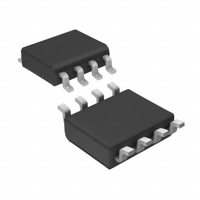
| 描述 | IC OPAMP JFET 1MHZ 8SO |
| 产品分类 | Linear - Amplifiers - Instrumentation, OP Amps, Buffer Amps |
| 品牌 | STMicroelectronics |
| 数据手册 | |
| 产品图片 |
|
| 产品型号 | TL062BCDT |
| rohs | 无铅 / 符合限制有害物质指令(RoHS)规范要求 |
| 产品系列 | - |
| 产品目录页面 | |
| 供应商器件封装 | 8-SO |
| 其它名称 | 497-7038-1 |
| 其它有关文件 | http://www.st.com/web/catalog/sense_power/FM123/SC61/SS1613/LN1588/PF247219?referrer=70071840http://www.st.com/web/catalog/sense_power/FM123/SC61/SS1378/PF247219?referrer=70071840 |
| 包装 | 剪切带 (CT) |
| 压摆率 | 3.5 V/µs |
| 增益带宽积 | 1MHz |
| 安装类型 | 表面贴装 |
| 封装/外壳 | 8-SOIC(0.154",3.90mm 宽) |
| 工作温度 | 0°C ~ 70°C |
| 放大器类型 | J-FET |
| 标准包装 | 1 |
| 电压-电源,单/双 (±) | 6 V ~ 36 V, ±3 V ~ 18 V |
| 电压-输入失调 | 2mV |
| 电流-电源 | 200µA |
| 电流-输入偏置 | 30pA |
| 电流-输出/通道 | 20mA |
| 电路数 | 2 |
| 输出类型 | - |


- 商务部:美国ITC正式对集成电路等产品启动337调查
- 曝三星4nm工艺存在良率问题 高通将骁龙8 Gen1或转产台积电
- 太阳诱电将投资9.5亿元在常州建新厂生产MLCC 预计2023年完工
- 英特尔发布欧洲新工厂建设计划 深化IDM 2.0 战略
- 台积电先进制程称霸业界 有大客户加持明年业绩稳了
- 达到5530亿美元!SIA预计今年全球半导体销售额将创下新高
- 英特尔拟将自动驾驶子公司Mobileye上市 估值或超500亿美元
- 三星加码芯片和SET,合并消费电子和移动部门,撤换高东真等 CEO
- 三星电子宣布重大人事变动 还合并消费电子和移动部门
- 海关总署:前11个月进口集成电路产品价值2.52万亿元 增长14.8%


PDF Datasheet 数据手册内容提取
TL062, TL062A, TL062B Low-power JFET dual operational amplifiers − Datasheet production data Features ■ Very low power consumption: 200µA ■ Wide common-mode (up to V +) and CC differential voltage ranges N ■ Low input bias and offset currents DIP8 (plastic package) ■ Output short-circuit protection ■ High input impedance JFET input stage ■ Internal frequency compensation ■ Latch up free operation D SO-8 ■ High slew rate: 3.5V/µs (plastic micropackage) Description The TL062, TL062A and TL062B devices are high-speed JFET input single operational Pin connections amplifiers. Each of these JFET input operational (top view) amplifiers incorporates well matched, high-voltage JFET and bipolar transistors in a monolithic integrated circuit. 1 8 The devices feature high slew rates, low input bias and offset currents, and a low offset voltage 2 - 7 temperature coefficient. 3 + - 6 4 + 5 1 - Output 1 2 - Inverting input 1 3 - Non-inverting input 1 4 - V - CC 5 - Non-inverting input 2 6 - Inverting input 2 7 - Output 2 8 - V + CC September 2012 Doc ID 2294 Rev 4 1/15 This is information on a product in full production. www.st.com 15
Schematic diagram TL062, TL062A, TL062B 1 Schematic diagram Figure 1. Schematic diagram 2/15 Doc ID 2294 Rev 4
TL062, TL062A, TL062B Absolute maximum ratings and operating conditions 2 Absolute maximum ratings and operating conditions T able 1. Absolute maximum ratings Symbol Parameter Value Unit V Supply voltage(1) ±18 V CC V Input voltage(2) ±15 V i V Differential input voltage(3) ±30 V id P Power dissipation 680 mW tot Output short-circuit duration(4) Infinite T Storage temperature range °C stg Thermal resistance junction-to-ambient(5),(6) Rthja SO-8 125 °C/W DIP8 85 Thermal resistance junction-to-case(5),(6) Rthjc SO-8 40 °C/W DIP8 41 HBM: human body model(7) 900 V ESD MM: machine model(8) 150 V CDM: charged device model(9) 1.5 kV 1. All voltage values, except differential voltage, are with respect to the zero reference level (ground) of the supply voltages where the zero reference level is the midpoint between V + and V -. CC CC 2. The magnitude of the input voltage must never exceed the magnitude of the supply voltage or 15 volts, whichever is less. 3. Differential voltages are the non-inverting input terminal with respect to the inverting input terminal. 4. The output may be shorted to ground or to either supply. Temperature and/or supply voltages must be limited to ensure that the dissipation rating is not exceeded. 5. Short-circuits can cause excessive heating and destructive dissipation. 6. R are typical values. th 7. Human body model: 100pF discharged through a 1.5kΩ resistor between two pins of the device, done for all couples of pin combinations with other pins floating. 8. Machine model: a 200pF capacitor is charged to the specified voltage, then discharged directly between two pins of the device with no external series resistor (internal resistor < 5Ω), done for all couples of pin combinations with other pins floating. 9. Charged device model: all pins plus package are charged together to the specified voltage and then discharged directly to ground. T a ble 2. Operating conditions Symbol Parameter TL062I, AI, BI TL062C, AC, BC Unit V Supply voltage range 6 to 36 V CC T Operating free air temperature range -40 to +105 0 to +70 °C oper Doc ID 2294 Rev 4 3/15
Electrical characteristics TL062, TL062A, TL062B 3 Electrical characteristics Table 3. V = ±15V, T = +25 °C (unless otherwise specified) CC amb TL062I TL062C Symbol Parameter Unit Min. Typ. Max. Min. Typ. Max. Input offset voltage (R = 50 Ω) S Vio Tamb = +25 °C 3 6 3 15 mV T ≤ T ≤ T 9 20 min amb max Temperature coefficient of input offset voltage DV 10 μV/°C io (R = 50 Ω) 10 S Input offset current(1) Iio Tamb = +25 °C 5 100 5 200 pA T ≤ T ≤ T 10 5 nA min amb max Input bias current(1) Iib Tamb = +25 °C 30 200 30 400 pA T ≤ T ≤ T 20 10 nA min amb max +15 +15 V Input common mode voltage range ±11.5 ±11.5 V icm -12 -12 Output voltage swing (R = 10 kΩ) L Vopp Tamb = +25 °C 20 27 20 27 V T ≤ T ≤ T 20 20 min amb max Large signal voltage gain R = 10 kΩ, V = ±10 V, A L o V/mV vd T = +25 °C 4 6 3 6 amb T ≤ T ≤ T 4 3 min amb max Gain bandwidth product GBP 1 1 MHz T = +25 °C, R =10 kΩ, C = 100 pF amb L L R Input resistance 1012 1012 Ω i Common mode rejection ratio CMR 80 86 70 76 dB R = 50 Ω S Supply voltage rejection ratio SVR 80 95 70 95 dB R = 50 Ω S Supply current, no load I 200 250 200 250 μA CC T = +25 °C, no load, no signal amb Channel separation V /V 120 120 dB o1 o2 A = 100, T = 25 °C v amb Total power consumption P 6 7.5 6 7.5 mW D T = +25 °C, no load, no signal amb Slew rate SR 1.5 3.5 1.5 3.5 V/μs V = 10 V, R = 10 kΩ, C = 100 pF, A = 1 i L L v 4/15 Doc ID 2294 Rev 4
TL062, TL062A, TL062B Electrical characteristics Table 3. V = ±15V, T = +25 °C (unless otherwise specified) (continued) CC amb TL062I TL062C Symbol Parameter Unit Min. Typ. Max. Min. Typ. Max. Rise time tr Vi = 20 mV, RL = 10 kΩ, 0.2 0.2 μs C = 100 pF, A = 1 L v Overshoot factor (see Figure15) K 10 10 % ov V = 20 mV, R = 10 kΩ, C = 100 pF, A = 1 i L L v Equivalent input noise voltage nV e 42 42 ------------ n R = 100 Ω, f = 1 kHz Hz S 1. The input bias currents of a FET-input operational amplifier are normal junction reverse currents, which are temperature sensitive. Pulse techniques must be used that will maintain the junction temperature as close to the ambient temperature as possible. Table 4. V = ±15V, T = +25 °C (unless otherwise specified) CC amb TL062AC, AI TL062BC, BI Symbol Parameter Unit Min. Typ. Max. Min. Typ. Max. Input offset voltage (R = 50 Ω) S Vio Tamb = +25 °C 3 3 2 3 mV T ≤ T ≤ T 7.5 5 min amb max Temperature coefficient of input offset voltage DV 10 10 µV/°C io (R = 50 Ω) S Input offset current(1) Iio Tamb = +25 °C 5 100 5 100 pA T ≤ T ≤ T 3 3 nA min amb max Input bias current(1) Iib Tamb = +25 °C 30 200 30 200 nA T ≤ T ≤ T 7 7 min amb max ±11.5 +15 ±11.5 +15 V Input common mode voltage range icm -12 -12 Output voltage swing (R = 10 kΩ) L Vopp Tamb = +25 °C 20 27 20 27 V T ≤ T ≤ T 20 20 min amb max Large signal voltage gain R = 10 kΩ, V = ±10 V, A L o V/mV vd T = +25 °C 4 6 4 6 amb T ≤ T ≤ T 4 4 min amb max Gain bandwidth product GBP 1 1 MHz T = +25 °C, R =10 kΩ, C = 100 pF amb L L R Input resistance 1012 1012 Ω i Common mode rejection ratio CMR 80 86 80 86 dB R = 50 Ω S Supply voltage rejection ratio SVR 80 95 80 95 dB R = 50 Ω S Doc ID 2294 Rev 4 5/15
Electrical characteristics TL062, TL062A, TL062B Table 4. V = ±15V, T = +25 °C (unless otherwise specified) (continued) CC amb TL062AC, AI TL062BC, BI Symbol Parameter Unit Min. Typ. Max. Min. Typ. Max. Supply current, no load I 200 250 200 250 µA CC T = +25 °C, no load, no signal amb Channel separation V /V 120 120 o1 o2 A = 100, T = +25 °C v amb Total power consumption P 6 7.5 6 7.5 mW D T = +25 °C, no load, no signal amb Slew rate SR 1.5 3.5 1.5 3.5 V/μs V = 10 V, R = 10 kΩ, C = 100 pF, A = 1 i L L v Rise time t 0.2 0.2 μs r V = 20 mV, R = 10 kΩ, C = 100 pF, A = 1 i L L v Overshoot factor (see Figure15) K 10 10 % ov V = 20 mV, R = 10 kΩ, C = 100 pF, A = 1 i L L v Equivalent input noise voltage en RS = 100 Ω, f = 1 kHz 42 42 ---n--H-V----z-- 1. The input bias currents of a FET-input operational amplifier are normal junction reverse currents, which are temperature sensitive. Pulse techniques must be used that will maintain the junction temperature as close to the ambient temperature as possible. 6/15 Doc ID 2294 Rev 4
TL062, TL062A, TL062B Electrical characteristics Figure 2. M aximum peak-to-peak output Figure 3. Maximum peak-to-peak output voltage versus supply voltage voltage versus free air temperature ut p ut out RL = 10 kΩ utp ak Tamb = + 25 °C k o m peak-to-pevoltage (V) m peak-to-peavoltage (V) VRCC = = 1 +0/ -k 1Ω5 V mu mu L axi axi M M Free air temperature (°C) Supply voltage (V) Figure 4. Maximum peak-to-peak output Figure 5. Maximum peak-to-peak output voltage versus load resistance voltage versus frequency ut ut utp utp RL = 10 kΩ k o k o VCC = +/- 15 V Tamb = + 25 °C a a peV) peV) m peak-to-voltage ( VCC = +/- 15 V m peak-to-voltage ( VVCCCC == ++//-- 152 V V mu Tamb = + 25 °C mu VCC = +/- 2 V xi xi a a M M Load resistance (kΩ) Frequency (Hz) Figure 6. Differential voltage amplification Figure 7. Large signal differential voltage versus free air temperature amplification and phase shift versus frequency 6 10 10 V = +/- 5 V to +/- 15 V CC Differential voltageamplification (V/mV) 247 VCRC == +1/0- 1k5Ω V Differential voltageamplification (V/V) 111110000032154 (Prihgahst es csahlieft) RTaLm =b =2 +k Ω25 °aCD(mleivfpffotel ilfsrtiaeccgnaaettlieiao)ln 91040355 L 1 180 -75 -50 -25 0 25 50 75 100 125 1 10 100 1k 10k 100k 1M 10M Free air temperature (°C) Frequency (Hz) Doc ID 2294 Rev 4 7/15
Electrical characteristics TL062, TL062A, TL062B Figure 8. S upply current per amplifier versus Figure 9. Supply current per amplifier versus supply voltage free air temperature 250 250 μA) 200 A) 200 ent ( 150 μnt ( 150 Supply curr 15000 TaNmbo = s +ig n2a5l °C Supply curre 15000 VCCN =o +si/g- n1a5l V no load no load 0 0 0 2 4 6 8 10 12 14 16 -75 -50 -25 0 25 50 75 100 125 Supply voltage (+/- V) Free air temperature (°C) Figure 10. Total power dissipated versus free Figure 11. Common-mode rejection ratio air temperature versus free air temperature 30 87 o ated 25 VCCN =o +si/g- n1a5l V on rati 86 sip 20 no load cti 85 s e power di(mW) 1105 mode rej(dB) 8834 Total 5 mon 82 VCRC = = + 1/-0 1k5Ω V m L o 0 C 81 -75 -50 -25 0 25 50 75 100 125 -75 -50 -25 0 25 50 75 100 125 Free air temperature (°C) Free air temperature (°C) Figure 12. Normalized unity gain bandwidth Figure 13. Input bias current versus free air slew rate and phase shift versus temperature temperature 100 h 1.3 1.03 malized unity-gain bandwidtand slew rate 0011....81129 VRf C=LUC =Bn= i1 1t+ yf0o/-(- glrk e 1aΩpf5itnh sV abcsaaelne sd)hwifidtth (Prihg(ahSlestl feest w cssa chrlaaiefltt)ee) 0011....990019812 Normalized phase shift Input bias current (nA) 011.01 VCC = +/- 15 V Nor 0.7-75 -50 -25 0 25 50 75 100 1250.97 0.01 -50 -25 0 25 50 75 100 125 Free air temperature (°C) Free air temperature (°C) 8/15 Doc ID 2294 Rev 4
TL062, TL062A, TL062B Electrical characteristics Figure 14. V oltage follower large signal pulse Figure 15. Output voltage versus elapsed time response 6 28 V) ages ( 4 Input mV) 2240 Overshoot 90% olt 2 Output e ( 16 v g put 0 V = +/ - 15 V olta 12 ut and out --42 RCTCLLaC m==b =1100 + 0k 2Ωp5F °C Output v 084 10% t VRTCaLCm =b= = 1+ 0+/ - k 21Ω55 °VC Inp -6 0 2 4 6 8 10 -4 0 0.2r 0.4 0.6 0.8 1 12 14 Time (μs) Time (μs) Figure 16. Equivalent input noise voltage versus frequency 100 90 e V = +/- 15 V oisz) 80 RCC = 100 Ω nH 70 S put V/V 60 Tamb = + 25 °C nt ine (n 5400 eg ala 30 uivvolt 20 q E 10 0 10 40 100 400 1k 4k 10k 40k 100k Frequency (Hz) Parameter measurement information Figure 17. Voltage follower Figure 18. Gain of 10 inverting amplifier 10 kΩ - 1 kΩ e - 1/2 I e 1/2 TL062 o e TL062 o e C = 100 pF R = 10 kΩ I L L R C = 100 pF L L Doc ID 2294 Rev 4 9/15
Typical applications TL062, TL062A, TL062B 4 Typical applications Figure 19. 100kHz quadrature oscillator 18 k Ω(1) 1N 4148 -15 V 18 pF 1 k Ω 18 pF - 1/2 88.4 k Ω - TL062 1/2 88.4 k Ω TL062 6 cos ω t 6 sin ω t 1 k Ω 18 pF 88.4 k Ω 1N 4148 18 k Ω( 1) +15 V 1. These resistor values may be adjusted for a symmetrical output. 10/15 Doc ID 2294 Rev 4
TL062, TL062A, TL062B Package information 5 Package information In order to meet environmental requirements, ST offers these devices in different grades of ECOPACK® packages, depending on their level of environmental compliance. ECOPACK specifications, grade definitions and product status are available at: www.st.com. ECOPACK is an ST trademark. Doc ID 2294 Rev 4 11/15
Package information TL062, TL062A, TL062B 5.1 DIP8 package information Figure 20. DIP8 package outline Table 5. DIP8 package mechanical data Dimensions Symbol Millimeters Inches Min. Typ. Max. Min. Typ. Max. A 5.33 0.210 A1 0.38 0.015 A2 2.92 3.30 4.95 0.115 0.130 0.195 b 0.36 0.46 0.56 0.014 0.018 0.022 b2 1.14 1.52 1.78 0.045 0.060 0.070 c 0.20 0.25 0.36 0.008 0.010 0.014 D 9.02 9.27 10.16 0.355 0.365 0.400 E 7.62 7.87 8.26 0.300 0.310 0.325 E1 6.10 6.35 7.11 0.240 0.250 0.280 e 2.54 0.100 eA 7.62 0.300 eB 10.92 0.430 L 2.92 3.30 3.81 0.115 0.130 0.150 Note: Dimensions "D" and "E1" do not include mold flash, protrusions or gate burrs. Mold flash, protrusions or gate burrs shall not exceed 0.25 mm in total (both sides). Datum plane "H" coincides with the bottom of the lead, where the lead exits the body. 12/15 Doc ID 2294 Rev 4
TL062, TL062A, TL062B Package information 5.2 SO-8 package information Figure 21. SO-8 package outline Table 6. SO-8 package mechanical data Dimensions Symbol Millimeters Inches Min. Typ. Max. Min. Typ. Max. A 1.75 0.069 A1 0.10 0.25 0.004 0.010 A2 1.25 0.049 b 0.28 0.48 0.011 0.019 c 0.17 0.23 0.007 0.010 D 4.80 4.90 5.00 0.189 0.193 0.197 E 5.80 6.00 6.20 0.228 0.236 0.244 E1 3.80 3.90 4.00 0.150 0.154 0.157 e 1.27 0.050 h 0.25 0.50 0.010 0.020 L 0.40 1.27 0.016 0.050 L1 1.04 0.040 k 0 8° 1° 8° ccc 0.10 0.004 Doc ID 2294 Rev 4 13/15
Ordering information TL062, TL062A, TL062B 6 Ordering information T able 7. Order codes Temperature Part number Package Packaging Marking range TL062IN TL062IN TL062AIN DIP8 Tube TL062AIN TL062BIN TL062BIN -40 °C, +105 °C TL062ID/IDT 062I Tube or TL062AID/AIDT SO-8 062AI tape and reel TL062BID/BIDT 062BI TL062CN TL062CN TL062ACN DIP8 Tube TL062ACN TL062BCN TL062BCN 0 °C, +70 °C TL062CD/CDT 062C Tube or TL062ACD/ACDT SO-8 062AC tape and reel TL062BCD/BCDT 062BC 7 Revision history T able 8. Document revision history Date Revision Changes 28-Mar-2001 1 Initial release. Added values for R and R in Table1: Absolute maximum thja thjc ratings. 27-Jul-2007 2 Added Table2: Operating conditions. Updated format. Updated document format. 15-Mar-2010 3 Added TL062A and TL062B in title on cover page. Updated package information in Chapter5. Removed TL062M, AM, BM /TL062I, AI, BI / TL062C, AC, BC part numbers and temperature ranges from Table1. and TL062M, AM, BM from Table2. Removed TL062M, updated min. “Input common mode voltage range” for TL062C device in Table3. 21-Sep-2012 4 Removed TL062AM and TL062BM devices, updated max. ”Input offset voltage - T ” for TL062AC, AI devices in Table4. amb Removed TL062MN, TL062AMN, TL062BMN, TL062MD/MDT, TL062AMD/AMDT, TL062BMD/BMDT part numbers from Table7. Minor corrections throughout document. 14/15 Doc ID 2294 Rev 4
TL062, TL062A, TL062B Please Read Carefully: Information in this document is provided solely in connection with ST products. STMicroelectronics NV and its subsidiaries (“ST”) reserve the right to make changes, corrections, modifications or improvements, to this document, and the products and services described herein at any time, without notice. All ST products are sold pursuant to ST’s terms and conditions of sale. Purchasers are solely responsible for the choice, selection and use of the ST products and services described herein, and ST assumes no liability whatsoever relating to the choice, selection or use of the ST products and services described herein. No license, express or implied, by estoppel or otherwise, to any intellectual property rights is granted under this document. If any part of this document refers to any third party products or services it shall not be deemed a license grant by ST for the use of such third party products or services, or any intellectual property contained therein or considered as a warranty covering the use in any manner whatsoever of such third party products or services or any intellectual property contained therein. UNLESS OTHERWISE SET FORTH IN ST’S TERMS AND CONDITIONS OF SALE ST DISCLAIMS ANY EXPRESS OR IMPLIED WARRANTY WITH RESPECT TO THE USE AND/OR SALE OF ST PRODUCTS INCLUDING WITHOUT LIMITATION IMPLIED WARRANTIES OF MERCHANTABILITY, FITNESS FOR A PARTICULAR PURPOSE (AND THEIR EQUIVALENTS UNDER THE LAWS OF ANY JURISDICTION), OR INFRINGEMENT OF ANY PATENT, COPYRIGHT OR OTHER INTELLECTUAL PROPERTY RIGHT. UNLESS EXPRESSLY APPROVED IN WRITING BY TWO AUTHORIZED ST REPRESENTATIVES, ST PRODUCTS ARE NOT RECOMMENDED, AUTHORIZED OR WARRANTED FOR USE IN MILITARY, AIR CRAFT, SPACE, LIFE SAVING, OR LIFE SUSTAINING APPLICATIONS, NOR IN PRODUCTS OR SYSTEMS WHERE FAILURE OR MALFUNCTION MAY RESULT IN PERSONAL INJURY, DEATH, OR SEVERE PROPERTY OR ENVIRONMENTAL DAMAGE. ST PRODUCTS WHICH ARE NOT SPECIFIED AS "AUTOMOTIVE GRADE" MAY ONLY BE USED IN AUTOMOTIVE APPLICATIONS AT USER’S OWN RISK. Resale of ST products with provisions different from the statements and/or technical features set forth in this document shall immediately void any warranty granted by ST for the ST product or service described herein and shall not create or extend in any manner whatsoever, any liability of ST. ST and the ST logo are trademarks or registered trademarks of ST in various countries. Information in this document supersedes and replaces all information previously supplied. The ST logo is a registered trademark of STMicroelectronics. All other names are the property of their respective owners. © 2012 STMicroelectronics - All rights reserved STMicroelectronics group of companies Australia - Belgium - Brazil - Canada - China - Czech Republic - Finland - France - Germany - Hong Kong - India - Israel - Italy - Japan - Malaysia - Malta - Morocco - Philippines - Singapore - Spain - Sweden - Switzerland - United Kingdom - United States of America www.st.com Doc ID 2294 Rev 4 15/15