ICGOO在线商城 > 集成电路(IC) > 接口 - 驱动器,接收器,收发器 > TJA1051TK/3,118

 Datasheet下载
- 型号: TJA1051TK/3,118
- 制造商: NXP Semiconductors
- 库位|库存: xxxx|xxxx
- 要求:
| 数量阶梯 | 香港交货 | 国内含税 |
| +xxxx | $xxxx | ¥xxxx |
查看当月历史价格
查看今年历史价格
TJA1051TK/3,118产品简介:
ICGOO电子元器件商城为您提供TJA1051TK/3,118由NXP Semiconductors设计生产,在icgoo商城现货销售,并且可以通过原厂、代理商等渠道进行代购。 TJA1051TK/3,118价格参考。NXP SemiconductorsTJA1051TK/3,118封装/规格:接口 - 驱动器,接收器,收发器, 1/1 Transceiver Half CANbus 8-HVSON (3x3)。您可以下载TJA1051TK/3,118参考资料、Datasheet数据手册功能说明书,资料中有TJA1051TK/3,118 详细功能的应用电路图电压和使用方法及教程。
NXP USA Inc. 的 TJA1051TK/3,118 是一款高速 CAN(控制器局域网)收发器,属于接口类器件中的驱动器、接收器、收发器类别。该器件主要作为微控制器与物理CAN总线之间的接口,广泛应用于需要可靠通信的汽车和工业场景。

TJA1051TK/3,118 主要用于汽车电子系统中,如车身控制模块(BCM)、发动机控制单元(ECU)、变速器控制、防抱死制动系统(ABS)、安全气囊系统、电动助力转向(EPS)等。其支持高速CAN通信(最高达1 Mbps),符合ISO 11898-2标准,具备良好的抗电磁干扰能力,适合在复杂电磁环境中稳定运行。

此外,该收发器集成有多种保护功能,包括总线引脚对地短路保护、对电池短路保护以及过热关断机制,提高了系统的可靠性与安全性。其采用SO8封装,体积小,便于集成在紧凑型电子控制单元中。

TJA1051TK/3,118 还支持低功耗待机模式,有助于降低整车静态电流,延长蓄电池寿命,特别适用于现代汽车对节能和智能化的高要求。在工业自动化领域,也可用于需要CAN通信的电机控制、远程I/O模块等设备。

总之,TJA1051TK/3,118 凭借高可靠性、优异的电气性能和丰富的保护功能,是汽车车载网络通信中的关键组件之一。
| 参数 | 数值 |
| 产品目录 | 集成电路 (IC)半导体 |
| 描述 | IC TXRX CAN HIGH SPEED 8HVSONCAN 接口集成电路 HIGH-SPEED CAN TRANSCEIVER |
| 产品分类 | |
| 品牌 | NXP Semiconductors |
| 产品手册 | |
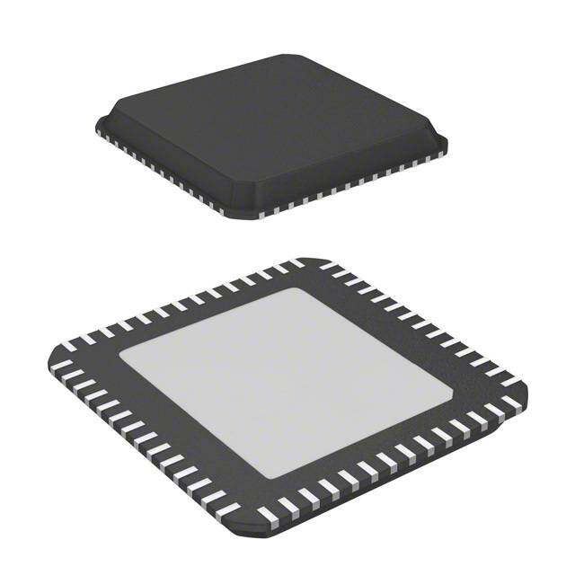
| 产品图片 |
|
| rohs | 符合RoHS无铅 / 符合限制有害物质指令(RoHS)规范要求 |
| 产品系列 | 接口 IC,CAN 接口集成电路,NXP Semiconductors TJA1051TK/3,118- |
| 数据手册 | |
| 产品型号 | TJA1051TK/3,118 |
| PCN组件/产地 | |
| 产品种类 | CAN 接口集成电路 |
| 供应商器件封装 | 8-HVSON(3x3) |
| 其它名称 | 568-8686-2 |
| 包装 | 带卷 (TR) |
| 协议 | CAN |
| 双工 | 半 |
| 商标 | NXP Semiconductors |
| 安装类型 | 表面贴装 |
| 封装 | Reel |
| 封装/外壳 | 8-VDFN 裸露焊盘 |
| 工作温度 | -40°C ~ 125°C |
| 工厂包装数量 | 6000 |
| 接收器滞后 | 120mV |
| 数据速率 | - |
| 标准包装 | 6,000 |
| 电压-电源 | 4.5 V ~ 5.5 V |
| 类型 | 收发器 |
| 驱动器/接收器数 | 1/1 |


- 商务部:美国ITC正式对集成电路等产品启动337调查
- 曝三星4nm工艺存在良率问题 高通将骁龙8 Gen1或转产台积电
- 太阳诱电将投资9.5亿元在常州建新厂生产MLCC 预计2023年完工
- 英特尔发布欧洲新工厂建设计划 深化IDM 2.0 战略
- 台积电先进制程称霸业界 有大客户加持明年业绩稳了
- 达到5530亿美元!SIA预计今年全球半导体销售额将创下新高
- 英特尔拟将自动驾驶子公司Mobileye上市 估值或超500亿美元
- 三星加码芯片和SET,合并消费电子和移动部门,撤换高东真等 CEO
- 三星电子宣布重大人事变动 还合并消费电子和移动部门
- 海关总署:前11个月进口集成电路产品价值2.52万亿元 增长14.8%


PDF Datasheet 数据手册内容提取
TJA1051 High-speed CAN transceiver Rev. 9 — 28 November 2017 Product data sheet 1. General description The TJA1051 is a high-speed CAN transceiver that provides an interface between a Controller Area Network (CAN) protocol controller and the physical two-wire CAN bus. The transceiver is designed for high-speedCAN applications in the automotive industry, providing differential transmit and receive capability to (a microcontroller with) a CAN protocol controller. The TJA1051 belongs to the third generation of high-speed CAN transceivers from NXP Semiconductors, offering significant improvements over first- and second-generation devices such as the TJA1050. It offers improved ElectroMagnetic Compatibility (EMC) and ElectroStatic Discharge (ESD) performance, and also features: • Ideal passive behavior to the CAN bus when the supply voltage is off • TJA1051T/3 and TJA1051TK/3 can be interfaced directly to microcontrollers with supply voltages from 3Vto5V The TJA1051 implements the CAN physical layer as defined in ISO 11898-2:2016 and SAE J2284-1 to SAE J2284-5. This implementation enables reliable communication in the CAN FD fast phase at data rates up to 5Mbit/s. These features make the TJA1051 an excellent choice for all types of HS-CAN networks, in nodes that do not require a standby mode with wake-up capability via the bus. 2. Features and benefits 2.1 General ISO 11898-2:2016 and SAE J2284-1 to SAE J2284-5 compliant Timing guaranteed for data rates up to 5Mbit/s in the CAN FD fast phase Suitable for 12V and 24V systems Low ElectroMagnetic Emission (EME) and high ElectroMagnetic Immunity (EMI) V input on TJA1051T/3 and TJA1051TK/3 allows for direct interfacing with 3Vto5V IO microcontrollers (available in SO8 and very small HVSON8 packages respectively) EN input on TJA1051T/E allows the microcontroller to switch the transceiver to a very low-current Off mode Available in SO8 package or leadless HVSON8 package (3.0 mm3.0mm) with improved Automated Optical Inspection (AOI) capability Dark green product (halogen free and Restriction of Hazardous Substances (RoHS) compliant) AEC-Q100 qualified
TJA1051 NXP Semiconductors High-speed CAN transceiver 2.2 Low-power management Functional behavior predictable under all supply conditions Transceiver disengages from the bus when not powered up (zero load) 2.3 Protection High ElectroStatic Discharge (ESD) handling capability on the bus pins Bus pins protected against transients in automotive environments Transmit Data (TXD) dominant time-out function Undervoltage detection on pinsV and V CC IO Thermally protected 3. Quick reference data Table 1. Quick reference data Symbol Parameter Conditions Min Typ Max Unit V supply voltage 4.5 - 5.5 V CC V supply voltage on pin V 2.8 - 5.5 V IO IO V undervoltage detection 3.5 - 4.5 V uvd(VCC) voltage on pin V CC V undervoltage detection 1.3 2.0 2.7 V uvd(VIO) voltage on pin V IO I supply current Silent mode 0.1 1 2.5 mA CC Normal mode; bus 2.5 5 10 mA recessive Normal mode; bus 20 50 70 mA dominant I supply current on pin V Normal/Silent mode IO IO recessive; V =V - 80 250 A TXD IO dominant; V =0V - 350 500 A TXD V electrostatic discharge IEC 61000-4-2 at pins 8 - +8 kV ESD voltage CANH and CANL V voltage on pin CANH 58 - +58 V CANH V voltage on pin CANL 58 - +58 V CANL T virtual junction temperature 40 - +150 C vj 4. Ordering information Table 2. Ordering info rmation Type number Package Name Description Version TJA1051T SO8 plastic small outline package; 8leads; body width 3.9mm SOT96-1 TJA1051 All information provided in this document is subject to legal disclaimers. © NXP N.V. 2017. All rights reserved. Product data sheet Rev. 9 — 28 November 2017 2 of 25
TJA1051 NXP Semiconductors High-speed CAN transceiver Table 2. Ordering information …continued Type number Package Name Description Version TJA1051T/3[1] SO8 plastic small outline package; 8leads; body width 3.9mm SOT96-1 TJA1051T/E[1] SO8 plastic small outline package; 8leads; body width 3.9mm SOT96-1 TJA1051TK/3[1] HVSON8 plastic thermal enhanced very thin small outline package; no leads; SOT782-1 8terminals; body 3 3 0.85 mm [1] TJA1051T/3 and TJA1051TK/3 with V pin; TJA1051T/E with EN pin. IO 5. Block diagram VIO(1) VCC 5 3 VCC TJA1051 TEMPERATURE PROTECTION VI/O(1) 7 CANH SLOPE CONTROL AND TXD 1 TIME-OUT DRIVER 6 CANL 8 S MODE CONTROL 5 EN(2) 4 RXD DRIVER 2 015aaa036 GND (1) In a transceiver without a V pin, the V input is internally connected to V . IO IO CC (2) Only present in the TJA1051T/E. Fig 1. Block diagram TJA1051 All information provided in this document is subject to legal disclaimers. © NXP N.V. 2017. All rights reserved. Product data sheet Rev. 9 — 28 November 2017 3 of 25
TJA1051 NXP Semiconductors High-speed CAN transceiver 6. Pinning information 6.1 Pinning (cid:55)(cid:45)(cid:36)(cid:20)(cid:19)(cid:24)(cid:20)(cid:55) (cid:55)(cid:45)(cid:36)(cid:20)(cid:19)(cid:24)(cid:20)(cid:55)(cid:18)(cid:40) (cid:55)(cid:59)(cid:39) (cid:20) (cid:27) (cid:54) (cid:55)(cid:59)(cid:39) (cid:20) (cid:27) (cid:54) (cid:42)(cid:49)(cid:39) (cid:21) (cid:26) (cid:38)(cid:36)(cid:49)(cid:43) (cid:42)(cid:49)(cid:39) (cid:21) (cid:26) (cid:38)(cid:36)(cid:49)(cid:43) (cid:57)(cid:38)(cid:38) (cid:22) (cid:25) (cid:38)(cid:36)(cid:49)(cid:47) (cid:57)(cid:38)(cid:38) (cid:22) (cid:25) (cid:38)(cid:36)(cid:49)(cid:47) (cid:53)(cid:59)(cid:39) (cid:23) (cid:24) (cid:81)(cid:17)(cid:70)(cid:17) (cid:53)(cid:59)(cid:39) (cid:23) (cid:24) (cid:40)(cid:49) (cid:19)(cid:20)(cid:24)(cid:68)(cid:68)(cid:68)(cid:21)(cid:21)(cid:24) (cid:19)(cid:20)(cid:24)(cid:68)(cid:68)(cid:68)(cid:21)(cid:21)(cid:22) a. TJA1051T: SO8 b. TJA1051T/E: SO8 (cid:87)(cid:72)(cid:85)(cid:80)(cid:76)(cid:81)(cid:68)(cid:79)(cid:3)(cid:20) (cid:55)(cid:45)(cid:36)(cid:20)(cid:19)(cid:24)(cid:20)(cid:55)(cid:46)(cid:18)(cid:22) (cid:55)(cid:45)(cid:36)(cid:20)(cid:19)(cid:24)(cid:20)(cid:55)(cid:18)(cid:22) (cid:76)(cid:81)(cid:71)(cid:72)(cid:91)(cid:3)(cid:68)(cid:85)(cid:72)(cid:68) (cid:55)(cid:59)(cid:39) (cid:20) (cid:27) (cid:54) (cid:55)(cid:59)(cid:39) (cid:20) (cid:27) (cid:54) (cid:42)(cid:49)(cid:39) (cid:21) (cid:26) (cid:38)(cid:36)(cid:49)(cid:43) (cid:42)(cid:49)(cid:39) (cid:21) (cid:26) (cid:38)(cid:36)(cid:49)(cid:43) (cid:57)(cid:38)(cid:38) (cid:22) (cid:25) (cid:38)(cid:36)(cid:49)(cid:47) (cid:57)(cid:38)(cid:38) (cid:22) (cid:25) (cid:38)(cid:36)(cid:49)(cid:47) (cid:53)(cid:59)(cid:39) (cid:23) (cid:24) (cid:57)(cid:44)(cid:50) (cid:53)(cid:59)(cid:39) (cid:23) (cid:24) (cid:57)(cid:44)(cid:50) (cid:68)(cid:68)(cid:68)(cid:16)(cid:19)(cid:20)(cid:19)(cid:23)(cid:23)(cid:24) (cid:19)(cid:20)(cid:24)(cid:68)(cid:68)(cid:68)(cid:21)(cid:21)(cid:23) (cid:55)(cid:85)(cid:68)(cid:81)(cid:86)(cid:83)(cid:68)(cid:85)(cid:72)(cid:81)(cid:87)(cid:3)(cid:87)(cid:82)(cid:83)(cid:3)(cid:89)(cid:76)(cid:72)(cid:90) c. TJA1051T/3: SO8 d. TJA1051TK/3: HVSON8 Fig 2. Pin configuration diagrams 6.2 Pin description Table 3. Pin description Symbol Pin Description TXD 1 transmit data input GND[1] 2 ground V 3 supply voltage CC RXD 4 receive data output; reads out data from the bus lines n.c. 5 not connected; in TJA1051T version EN 5 enable control input; TJA1051T/E only V 5 supply voltage for I/O level adapter; TJA1051T/3 and TJA1051TK/3 only IO CANL 6 LOW-level CAN bus line CANH 7 HIGH-level CAN bus line S 8 Silent mode control input [1] HVSON8 package die supply ground is connected to both the GND pin and the exposed center pad. The GND pin must be soldered to board ground. For enhanced thermal and electrical performance, it is recommended that the exposed center pad also be soldered to board ground. TJA1051 All information provided in this document is subject to legal disclaimers. © NXP N.V. 2017. All rights reserved. Product data sheet Rev. 9 — 28 November 2017 4 of 25
TJA1051 NXP Semiconductors High-speed CAN transceiver 7. Functional description The TJA1051 is a high-speed CAN stand-alone transceiver with Silent mode. It combines the functionality of the TJA1050 transceiver with improved EMC and ESD handling capability. Improved slope control and high DC handling capability on the bus pins provides additional application flexibility. The TJA1051 is available in three versions, distinguished only by the function of pin 5: • The TJA1051T is backwards compatible with the TJA1050 • The TJA1051T/3 and TJA1051TK/3 allow for direct interfacing to microcontrollers with supply voltages down to 3 V • The TJA1051T/E allows the transceiver to be switched to a very low-current Off mode. 7.1 Operating modes The TJA1051 supports two operating modes, Normal and Silent, which are selected via pin S. An additional Off mode is supported in the TJA1051T/E via pin EN. See Table4 for a description of the operating modes under normal supply conditions. Table 4. Operating modes Mode Inputs Outputs Pin EN[1] Pin S Pin TXD CAN driver Pin RXD Normal HIGH LOW LOW dominant active[2] HIGH LOW HIGH recessive active[2] Silent HIGH HIGH X[3] recessive active[2] Off[1] LOW X[3] X[3] floating floating [1] Only available on the TJA1051T/E. [2] LOW if the CAN bus is dominant, HIGH if the CAN bus is recessive. [3] ‘X’ = don’t care. 7.1.1 Normal mode A LOW level on pin S selects Normal mode. In this mode, the transceiver is able to transmit and receive data via the bus lines CANH and CANL (see Figure1 for the block diagram). The differential receiver converts the analog data on the bus lines into digital data which is output to pin RXD. The slopes of the output signals on the bus lines are controlled internally and are optimized in a way that guarantees the lowest possible ElectroMagnetic Emission (EME). 7.1.2 Silent mode A HIGH level on pin S selects Silent mode. In Silent mode the transmitter is disabled, releasing the bus pins to recessive state. All other IC functions, including the receiver, continue to operate as in Normal mode. Silent mode can be used to prevent a faulty CAN controller from disrupting all network communications. TJA1051 All information provided in this document is subject to legal disclaimers. © NXP N.V. 2017. All rights reserved. Product data sheet Rev. 9 — 28 November 2017 5 of 25
TJA1051 NXP Semiconductors High-speed CAN transceiver 7.1.3 Off mode A LOW level on pin EN of TJA1051T/E selects Off mode. In Off mode the entire transceiver is disabled, allowing the microcontroller to save power when CAN communication is not required. The bus pins are floating in Off mode, making the transceiver invisible to the rest of the network. 7.2 Fail-safe features 7.2.1 TXD dominant time-out function A ‘TXD dominant time-out’ timer is started when pinTXD is set LOW. If the LOW state on pinTXD persists for longer than t , the transmitter is disabled, releasing the bus to(dom)TXD lines to recessive state. This function prevents a hardware and/or software application failure from driving the bus lines to a permanent dominant state (blocking all network communications). The TXD dominant time-out timer is reset when pinTXD is set HIGH. The TXD dominant time-out time also defines the minimum possible bit rate of 20kbit/s. 7.2.2 Internal biasing of TXD, S and EN input pins Pin TXD has an internal pull-up to V and pins S and EN (TJA1051T/E) have internal IO pull-downs to GND. This ensures a safe, defined state in case one or more of these pins is left floating. 7.2.3 Undervoltage detection on pins V and V CC IO Should V or V drop below their respective undervoltage detection levels (V CC IO uvd(VCC) and V ; see Table7), the transceiver will switch off and disengage from the bus uvd (VIO) (zero load) until V and V have recovered. CC IO 7.2.4 Overtemperature protection The output drivers are protected against overtemperature conditions. If the virtual junction temperature exceeds the shutdown junction temperature, T , the output drivers will be j(sd) disabled until the virtual junction temperature falls below T and TXD becomes j(sd) recessive again. Including the TXD condition ensures that output driver oscillations due to temperature drift are avoided. 7.3 V supply pin IO There are three versions of the TJA1051 available, only differing in the function of a single pin. Pin 5 is either an enable control input (EN), a V supply pin or is not connected. IO Pin V on the TJA1051T/3 and TJA1051TK/3 should be connected to the microcontroller IO supply voltage (see Figure6). This will adjust the signal levels of pins TXD, RXD and S to the I/O levels of the microcontroller. For versions of the TJA1051 without a V pin, the V IO IO input is internally connected to V . This sets the signal levels of pins TXD, RXD and S to CC levels compatible with 5 V microcontrollers. TJA1051 All information provided in this document is subject to legal disclaimers. © NXP N.V. 2017. All rights reserved. Product data sheet Rev. 9 — 28 November 2017 6 of 25
TJA1051 NXP Semiconductors High-speed CAN transceiver 8. Limiting values Table 5. Limiting valu es In accordance with the Absolute Maximum Rating System (IEC 60134). All voltages are referenced to GND. Symbol Parameter Conditions Min Max Unit V voltage on pinx[1] on pins CANH, CANL 58 +58 V x on any other pin 0.3 +7 V V voltage between pin CANH 27 +27 V (CANH-CANL) and pin CANL V transient voltage on pins CANH, CANL [2] trt pulse 1 100 - V pulse 2a - 75 V pulse 3a 150 - V pulse 3b - 100 V V electrostatic discharge voltage IEC 61000-4-2 (150pF, 330) [3] ESD at pins CANH and CANL 8 +8 kV Human Body Model (HBM); 100pF, 1.5k [4] at pins CANH and CANL 8 +8 kV at any other pin 4 +4 kV Machine Model (MM); 200 pF, 0.75 H, 10 [5] at any pin 300 +300 V Charged Device Model (CDM); field Induced [6] charge; 4 pF at corner pins 750 +750 V at any pin 500 +500 V T virtual junction temperature [7] 40 +150 C vj T storage temperature 55 +150 C stg [1] The device can sustain voltages up to the specified values over the product lifetime, provided applied voltages (including transients) never exceed these values. [2] According to IEC TS 62228 (2007), Section 4.2.4; parameters for standard pulses defined in ISO7637 part 2: 2004-06. [3] According to IEC TS 62228 (2007), Section 4.3; DIN EN 61000-4-2. [4] According to AEC-Q100-002. [5] According to AEC-Q100-003. [6] AEC-Q100-011 Rev-C1. The classification level is C4B. [7] In accordance with IEC 60747-1. An alternative definition of virtual junction temperature is: Tvj=Tamb+PRth(vj-a), where Rth(vj-a) is a fixed value to be used for the calculation of Tvj. The rating for Tvj limits the allowable combinations of power dissipation (P) and ambient temperature (T ). amb 9. Thermal characteristics Table 6. Thermal cha racteristics According to IEC 60747-1. Symbol Parameter Conditions Value Unit R thermal resistance from virtual junction to ambient SO8 package; in free air 155 K/W th(vj-a) HVSON8 package; in free air 55 K/W TJA1051 All information provided in this document is subject to legal disclaimers. © NXP N.V. 2017. All rights reserved. Product data sheet Rev. 9 — 28 November 2017 7 of 25
TJA1051 NXP Semiconductors High-speed CAN transceiver 10. Static characteristics Table 7. Static charac teristics T =40C to+150C; V =4.5V to 5.5V; V =2.8V to 5.5V[1]; R =60 unless specified otherwise; All voltages are vj CC IO L defined with respect to ground; Positive currents flow into the IC[2]. Symbol Parameter Conditions Min Typ Max Unit Supply; pinV CC V supply voltage 4.5 - 5.5 V CC I supply current Off mode (TJA1051T/E) 1 5 8 A CC Silent mode 0.1 1 2.5 mA Normal mode recessive; V =V [3] - 5 10 mA TXD IO dominant; V =0V - 50 70 mA TXD dominant; V =0V; 2.5 80 110 mA TXD short circuit on bus lines; 3V V = V ) +18V CANH CANL V undervoltage detection 3.5 - 4.5 V uvd(VCC) voltage on pin V CC I/O level adapter supply; pinV [1] IO V supply voltage on pin V 2.8 - 5.5 V IO IO I supply current on pin V Normal/Silent mode IO IO recessive; V =V [3] - 80 250 A TXD IO dominant; V =0V - 350 500 A TXD V undervoltage detection 1.3 2.0 2.7 V uvd(VIO) voltage on pin V IO Mode control inputs; pins S and EN[4] V HIGH-level input voltage [5] 0.7V [3] - V +0.3[3] V IH IO IO V LOW-level input voltage 0.3 - 0.3V [3] V IL IO I HIGH-level input current V =V ; V =V [3] 1 4 10 A IH S IO EN IO I LOW-level input current V =0V; V =0 V 1 0 +1 A IL S EN CAN transmit data input; pinTXD V HIGH-level input voltage [5] 0.7V [3] - V +0.3[3] V IH IO IO V LOW-level input voltage 0.3 - +0.3V [3] V IL IO I HIGH-level input current V =V [3] 5 0 +5 A IH TXD IO I LOW-level input current Normal mode; V =0V 260 150 30 A IL TXD C input capacitance [6] - 5 10 pF i CAN receive data output; pinRXD I HIGH-level output current V =V 0.4V[3] 8 3 1 mA OH RXD IO I LOW-level output current V =0.4V; bus dominant 2 5 12 mA OL RXD Bus lines; pinsCANH and CANL V dominant output voltage V =0V; t<t O(dom) TXD to(dom)TXD pinCANH; R =50 to 65 2.75 3.5 4.5 V L pinCANL; R =50 to 65 0.5 1.5 2.25 V L V transmitter dominant voltage V = V V V 400 - +400 mV dom(TX)sym dom(TX)sym CC CANH CANL symmetry TJA1051 All information provided in this document is subject to legal disclaimers. © NXP N.V. 2017. All rights reserved. Product data sheet Rev. 9 — 28 November 2017 8 of 25
TJA1051 NXP Semiconductors High-speed CAN transceiver Table 7. Static characteristics …continued T =40C to+150C; V =4.5V to 5.5V; V =2.8V to 5.5V[1]; R =60 unless specified otherwise; All voltages are vj CC IO L defined with respect to ground; Positive currents flow into the IC[2]. Symbol Parameter Conditions Min Typ Max Unit V transmitter voltage symmetry V = V +V ; [6] 0.9V - 1.1V V TXsym TXsym CANH CANL CC CC f =250kHz, 1MHz and 2.5MHz; [7] TXD V = 4.75V to 5.25V; CC C =4.7nF SPLIT V differential output voltage dominant: Normal mode; V =0V; O(dif) TXD t<t ; V = 4.75V to 5.25V to(dom)TXD CC R =45to65 1.5 - 3 V L R =45to70 1.5 - 3.3 V L R =2240 1.5 - 5 V L recessive; no load Normal mode: V =V [3] 50 - +50 mV TXD IO V recessive output voltage Normal/Silent mode; V =V [3]; 2 0.5V 3 V O(rec) TXD IO CC noload V differential receiver threshold Normal/Silent mode; 0.5 0.7 0.9 V th(RX)dif voltage 30VV +30V; CANL 30VV +30V CANH V receiver recessive voltage Normal/Silent mode; 4 - 0.5 V rec(RX) 30VV +30V; CANL 30VV +30V CANH V receiver dominant voltage Normal/Silent mode; 0.9 - 9.0 V dom(RX) 30VV +30V; CANL 30VV +30V CANH V differential receiver Normal/Silent mode; 50 120 200 mV hys(RX)dif hysteresis voltage 30VV +30V; CANL 30VV +30V CANH I dominant short-circuit output V =0V; t<t ; V =5 V O(sc)dom TXD to(dom)TXD CC current pinCANH; V =15V to 100 70 40 mA CANH +40V pinCANL; V =15V to +40V 40 70 100 mA CANL I recessive short-circuit output Normal/Silent mode; V =V [3]; 5 - +5 mA O(sc)rec TXD IO current V =V =27V to +32V CANH CANL I leakage current V =V =0V or V =V = 5 0 +5 A L CC IO CC IO shorted to ground via 47 k; V =V =5V CANH CANL R input resistance 2V V +7V; [6] 9 15 28 k i CANL 2V V +7V CANH R input resistance deviation 0V V +5V; [6] 1 - +1 % i CANL 0V V +5V CANH R differential input resistance 2V V +7V; [6] 19 30 52 k i(dif) CANL 2V V +7V CANH C common-mode input [6] - - 20 pF i(cm) capacitance TJA1051 All information provided in this document is subject to legal disclaimers. © NXP N.V. 2017. All rights reserved. Product data sheet Rev. 9 — 28 November 2017 9 of 25
TJA1051 NXP Semiconductors High-speed CAN transceiver Table 7. Static characteristics …continued T =40C to+150C; V =4.5V to 5.5V; V =2.8V to 5.5V[1]; R =60 unless specified otherwise; All voltages are vj CC IO L defined with respect to ground; Positive currents flow into the IC[2]. Symbol Parameter Conditions Min Typ Max Unit C differential input capacitance [6] - - 10 pF i(dif) Temperature protection T shutdown junction [6] - 190 - C j(sd) temperature [1] Only TJA1051T/3 and TJA1051TK/3 have a V pin. In transceivers without a V pin, the V input is internally connected to V . IO IO IO CC [2] All parameters are guaranteed over the virtual junction temperature range by design. Factory testing uses correlated test conditions to cover the specified temperature and power supply voltage range. [3] V =V for the non-V product variants TJA1051T(/E) IO CC IO [4] Only TJA1051T/E has an EN pin. [5] Maximum value assumes V <V ; if V >V , the maximum value will be V + 0.3 V. CC IO CC IO CC [6] Not tested in production; guaranteed by design. [7] The test circuit used to measure the bus output voltage symmetry (which includes C ) is shown in Figure8. SPLIT 11. Dynamic characteristics Table 8. Dynamic cha racteristics T =40C to+150C; V =4.5V to5.5V; V =2.8V to5.5V[1]; R =60 unless specified otherwise. All voltages are vj CC IO L defined with respect to ground. Positive currents flow into theIC.[2] Symbol Parameter Conditions Min Typ Max Unit Transceiver timing; pins CANH, CANL, TXD and RXD; see Figure7 and Figure3 t delay time from TXD to bus dominant Normal mode - 65 - ns d(TXD-busdom) t delay time from TXD to bus recessive Normal mode - 90 - ns d(TXD-busrec) t delay time from bus dominant to RXD Normal/Silent mode - 60 - ns d(busdom-RXD) t delay time from bus recessive to RXD Normal/Silent mode - 65 - ns d(busrec-RXD) t delay time from TXD LOW to RXD LOW Normal mode: versions 40 - 250 ns d(TXDL-RXDL) with V pin IO Normalmode: other 40 - 220 ns versions t delay time from TXD HIGH to RXD HIGH Normal mode: versions 40 - 250 ns d(TXDH-RXDH) with V pin IO Normalmode: other 40 - 220 ns versions t transmitted recessive bit width t = 500ns [3] 435 - 530 ns bit(bus) bit(TXD) t = 200ns [3] 155 - 210 ns bit(TXD) t bit time on pin RXD t = 500ns [3] 400 - 550 ns bit(RXD) bit(TXD) t = 200ns [3] 120 - 220 ns bit(TXD) t receiver timing symmetry t = 500ns 65 - +40 ns rec bit(TXD) t = 200ns 45 - +15 ns bit(TXD) t TXD dominant time-out time V =0V; Normal mode [4] 0.3 1 5 ms to(dom)TXD TXD [1] Only TJA1051T/3 and TJA1051TK/3 have a V pin. In transceivers without a V pin, the V input is internally connected to V . IO IO IO CC [2] All parameters are guaranteed over the virtual junction temperature range by design. Factory testing uses correlated test conditions to cover the specified temperature and power supply voltage range. TJA1051 All information provided in this document is subject to legal disclaimers. © NXP N.V. 2017. All rights reserved. Product data sheet Rev. 9 — 28 November 2017 10 of 25
TJA1051 NXP Semiconductors High-speed CAN transceiver [3] See Figure4. [4] Minimum value of 0.8ms required according to SAE J2284; 0.3ms is allowed according to ISO11898-2:2016 for legacy devices. (cid:43)(cid:44)(cid:42)(cid:43) (cid:26)(cid:19)(cid:3)(cid:8) (cid:55)(cid:59)(cid:39) (cid:22)(cid:19)(cid:3)(cid:8) (cid:47)(cid:50)(cid:58) (cid:38)(cid:36)(cid:49)(cid:43) (cid:38)(cid:36)(cid:49)(cid:47) (cid:71)(cid:82)(cid:80)(cid:76)(cid:81)(cid:68)(cid:81)(cid:87) (cid:19)(cid:17)(cid:28)(cid:3)(cid:57) (cid:57)(cid:50)(cid:11)(cid:71)(cid:76)(cid:73)(cid:12) (cid:19)(cid:17)(cid:24)(cid:3)(cid:57) (cid:85)(cid:72)(cid:70)(cid:72)(cid:86)(cid:86)(cid:76)(cid:89)(cid:72) (cid:43)(cid:44)(cid:42)(cid:43) (cid:26)(cid:19)(cid:3)(cid:8) (cid:53)(cid:59)(cid:39) (cid:22)(cid:19)(cid:3)(cid:8) (cid:47)(cid:50)(cid:58) (cid:87)(cid:71)(cid:11)(cid:55)(cid:59)(cid:39)(cid:16)(cid:69)(cid:88)(cid:86)(cid:71)(cid:82)(cid:80)(cid:12) (cid:87)(cid:71)(cid:11)(cid:55)(cid:59)(cid:39)(cid:16)(cid:69)(cid:88)(cid:86)(cid:85)(cid:72)(cid:70)(cid:12) (cid:87)(cid:71)(cid:11)(cid:69)(cid:88)(cid:86)(cid:71)(cid:82)(cid:80)(cid:16)(cid:53)(cid:59)(cid:39)(cid:12) (cid:87)(cid:71)(cid:11)(cid:69)(cid:88)(cid:86)(cid:85)(cid:72)(cid:70)(cid:16)(cid:53)(cid:59)(cid:39)(cid:12) (cid:87)(cid:71)(cid:11)(cid:55)(cid:59)(cid:39)(cid:47)(cid:16)(cid:53)(cid:59)(cid:39)(cid:47)(cid:12) (cid:87)(cid:71)(cid:11)(cid:55)(cid:59)(cid:39)(cid:43)(cid:16)(cid:53)(cid:59)(cid:39)(cid:43)(cid:12) (cid:68)(cid:68)(cid:68)(cid:16)(cid:19)(cid:21)(cid:25)(cid:26)(cid:25)(cid:23) Fig 3. CAN transceiver timing diagram TJA1051 All information provided in this document is subject to legal disclaimers. © NXP N.V. 2017. All rights reserved. Product data sheet Rev. 9 — 28 November 2017 11 of 25
TJA1051 NXP Semiconductors High-speed CAN transceiver (cid:26)(cid:19)(cid:3)(cid:8) (cid:55)(cid:59)(cid:39) (cid:22)(cid:19)(cid:3)(cid:8) (cid:22)(cid:19)(cid:3)(cid:8) (cid:24)(cid:3)(cid:91)(cid:3)(cid:87)(cid:69)(cid:76)(cid:87)(cid:11)(cid:55)(cid:59)(cid:39)(cid:12) (cid:87)(cid:69)(cid:76)(cid:87)(cid:11)(cid:55)(cid:59)(cid:39)(cid:12) (cid:57)(cid:50)(cid:11)(cid:71)(cid:76)(cid:73)(cid:12) (cid:19)(cid:17)(cid:28)(cid:3)(cid:57) (cid:19)(cid:17)(cid:24)(cid:3)(cid:57) (cid:87)(cid:69)(cid:76)(cid:87)(cid:11)(cid:69)(cid:88)(cid:86)(cid:12) (cid:26)(cid:19)(cid:3)(cid:8) (cid:53)(cid:59)(cid:39) (cid:22)(cid:19)(cid:3)(cid:8) (cid:87)(cid:69)(cid:76)(cid:87)(cid:11)(cid:53)(cid:59)(cid:39)(cid:12) (cid:68)(cid:68)(cid:68)(cid:16)(cid:19)(cid:21)(cid:20)(cid:23)(cid:25)(cid:26) Fig 4. CAN FD timing definitions according to ISO 11898-2:2016 12. Application information 12.1 Application diagrams (cid:37)(cid:36)(cid:55) (cid:24)(cid:3)(cid:57) (cid:11)(cid:20)(cid:12) (cid:57)(cid:38)(cid:38) (cid:38)(cid:36)(cid:49)(cid:43) (cid:40)(cid:49) (cid:57)(cid:39)(cid:39) (cid:38)(cid:36)(cid:49)(cid:43) (cid:51)(cid:91)(cid:91) (cid:54) (cid:51)(cid:92)(cid:92) (cid:48)(cid:44)(cid:38)(cid:53)(cid:50)(cid:16) (cid:55)(cid:45)(cid:36)(cid:20)(cid:19)(cid:24)(cid:20)(cid:55)(cid:18)(cid:40) (cid:55)(cid:59)(cid:39) (cid:38)(cid:50)(cid:49)(cid:55)(cid:53)(cid:50)(cid:47)(cid:47)(cid:40)(cid:53) (cid:55)(cid:59)(cid:19) (cid:38)(cid:36)(cid:49)(cid:47) (cid:53)(cid:59)(cid:39) (cid:38)(cid:36)(cid:49)(cid:47) (cid:53)(cid:59)(cid:19) (cid:42)(cid:49)(cid:39) (cid:42)(cid:49)(cid:39) (cid:19)(cid:20)(cid:24)(cid:68)(cid:68)(cid:68)(cid:21)(cid:21)(cid:25) (1) Optional, depends on regulator. Fig 5. Typical application of the TJA1051T/E TJA1051 All information provided in this document is subject to legal disclaimers. © NXP N.V. 2017. All rights reserved. Product data sheet Rev. 9 — 28 November 2017 12 of 25
TJA1051 NXP Semiconductors High-speed CAN transceiver (cid:37)(cid:36)(cid:55) (cid:22)(cid:3)(cid:57) (cid:11)(cid:20)(cid:12) (cid:82)(cid:81)(cid:18)(cid:82)(cid:73)(cid:73)(cid:3)(cid:70)(cid:82)(cid:81)(cid:87)(cid:85)(cid:82)(cid:79) (cid:24)(cid:3)(cid:57) (cid:11)(cid:20)(cid:12) (cid:57)(cid:38)(cid:38) (cid:57)(cid:44)(cid:50) (cid:38)(cid:36)(cid:49)(cid:43) (cid:57)(cid:39)(cid:39) (cid:38)(cid:36)(cid:49)(cid:43) (cid:51)(cid:91)(cid:91) (cid:54) (cid:55)(cid:45)(cid:36)(cid:20)(cid:19)(cid:24)(cid:20)(cid:55)(cid:18)(cid:22) (cid:51)(cid:92)(cid:92) (cid:48)(cid:44)(cid:38)(cid:53)(cid:50)(cid:16) (cid:55)(cid:45)(cid:36)(cid:20)(cid:19)(cid:24)(cid:20)(cid:55)(cid:46)(cid:18)(cid:22) (cid:55)(cid:59)(cid:39) (cid:38)(cid:50)(cid:49)(cid:55)(cid:53)(cid:50)(cid:47)(cid:47)(cid:40)(cid:53) (cid:55)(cid:59)(cid:19) (cid:38)(cid:36)(cid:49)(cid:47) (cid:53)(cid:59)(cid:39) (cid:38)(cid:36)(cid:49)(cid:47) (cid:53)(cid:59)(cid:19) (cid:42)(cid:49)(cid:39) (cid:42)(cid:49)(cid:39) (cid:19)(cid:20)(cid:24)(cid:68)(cid:68)(cid:68)(cid:21)(cid:21)(cid:26) (1) Optional, depends on regulator. Fig 6. Typical application of the TJA1051T/3 or TJA1051TK/3. 12.2 Application hints Further information on the application of the TJA1051 can be found in NXP application hints AH1014 Application Hints - Standalone high speed CAN transceiver TJA1042/TJA1043/TJA1048/TJA1051. 13. Test information +5 V 47 μF 100 nF VIO/EN(1) VCC TXD CANH TJA1051 RL 100 pF RXD CANL GND S 15 pF 015aaa040 (1) For versions with a V pin (TJA1051T/3 and TJA1051TK/3) or an EN pin (TJA1051T/E), these IO inputs are connected to pin VCC. Fig 7. Timing test circuit for CAN transceiver TJA1051 All information provided in this document is subject to legal disclaimers. © NXP N.V. 2017. All rights reserved. Product data sheet Rev. 9 — 28 November 2017 13 of 25
TJA1051 NXP Semiconductors High-speed CAN transceiver (cid:57)(cid:38)(cid:38) (cid:57)(cid:44)(cid:50) (cid:22) (cid:24) (cid:55)(cid:59)(cid:39) (cid:38)(cid:36)(cid:49)(cid:43) (cid:20) (cid:26) (cid:73)(cid:3)(cid:32)(cid:3)(cid:21)(cid:24)(cid:19)(cid:3)(cid:78)(cid:43)(cid:93)(cid:15) (cid:22)(cid:19)(cid:3)(cid:525) (cid:20)(cid:3)(cid:48)(cid:43)(cid:93)(cid:3)(cid:82)(cid:85) (cid:21)(cid:17)(cid:24)(cid:3)(cid:48)(cid:43)(cid:93) (cid:55)(cid:45)(cid:36)(cid:20)(cid:19)(cid:24)(cid:20) (cid:38)(cid:54)(cid:51)(cid:47)(cid:44)(cid:55) (cid:23)(cid:17)(cid:26)(cid:3)(cid:81)(cid:41) (cid:22)(cid:19)(cid:3)(cid:525) (cid:53)(cid:59)(cid:39) (cid:38)(cid:36)(cid:49)(cid:47) (cid:23) (cid:25) (cid:21) (cid:42)(cid:49)(cid:39) (cid:68)(cid:68)(cid:68)(cid:16)(cid:19)(cid:21)(cid:21)(cid:27)(cid:28)(cid:19) Fig 8. Test circuit for measuring transceiver driver symmetry 13.1 Quality information This product has been qualified in accordance with the Automotive Electronics Council (AEC) standard Q100 Rev-G - Failure mechanism based stress test qualification for integrated circuits, and is suitable for use in automotive applications. TJA1051 All information provided in this document is subject to legal disclaimers. © NXP N.V. 2017. All rights reserved. Product data sheet Rev. 9 — 28 November 2017 14 of 25
TJA1051 NXP Semiconductors High-speed CAN transceiver 14. Package outline (cid:54)(cid:50)(cid:27)(cid:29)(cid:3)(cid:83)(cid:79)(cid:68)(cid:86)(cid:87)(cid:76)(cid:70)(cid:3)(cid:86)(cid:80)(cid:68)(cid:79)(cid:79)(cid:3)(cid:82)(cid:88)(cid:87)(cid:79)(cid:76)(cid:81)(cid:72)(cid:3)(cid:83)(cid:68)(cid:70)(cid:78)(cid:68)(cid:74)(cid:72)(cid:30)(cid:3)(cid:27)(cid:3)(cid:79)(cid:72)(cid:68)(cid:71)(cid:86)(cid:30)(cid:3)(cid:69)(cid:82)(cid:71)(cid:92)(cid:3)(cid:90)(cid:76)(cid:71)(cid:87)(cid:75)(cid:3)(cid:22)(cid:17)(cid:28)(cid:3)(cid:80)(cid:80)(cid:3) (cid:54)(cid:50)(cid:55)(cid:28)(cid:25)(cid:16)(cid:20)(cid:3) (cid:39)(cid:3) (cid:40)(cid:3) (cid:36)(cid:3) (cid:59)(cid:3) (cid:70)(cid:3) (cid:92)(cid:3) (cid:43)(cid:3)(cid:40)(cid:3) (cid:89)(cid:3)(cid:48)(cid:3) (cid:36)(cid:3) (cid:61)(cid:3) (cid:27)(cid:3) (cid:24)(cid:3) (cid:52)(cid:3) (cid:36)(cid:3)(cid:21)(cid:3)(cid:36)(cid:3)(cid:20)(cid:3) (cid:11)(cid:36)(cid:3)(cid:22)(cid:3)(cid:3)(cid:12)(cid:3) (cid:36)(cid:3) (cid:83)(cid:76)(cid:81)(cid:3)(cid:20)(cid:3)(cid:76)(cid:81)(cid:71)(cid:72)(cid:91)(cid:3) (cid:537)(cid:3) (cid:47)(cid:3)(cid:83)(cid:3) (cid:20)(cid:3) (cid:23)(cid:3) (cid:47)(cid:3) (cid:72)(cid:3) (cid:90)(cid:3)(cid:48)(cid:3) (cid:71)(cid:72)(cid:87)(cid:68)(cid:76)(cid:79)(cid:3)(cid:59)(cid:3) (cid:69)(cid:3)(cid:83)(cid:3) (cid:19)(cid:3) (cid:21)(cid:17)(cid:24)(cid:3) (cid:24)(cid:3)(cid:80)(cid:80)(cid:3) (cid:86)(cid:70)(cid:68)(cid:79)(cid:72)(cid:3) (cid:39)(cid:44)(cid:48)(cid:40)(cid:49)(cid:54)(cid:44)(cid:50)(cid:49)(cid:54)(cid:3)(cid:11)(cid:76)(cid:81)(cid:70)(cid:75)(cid:3)(cid:71)(cid:76)(cid:80)(cid:72)(cid:81)(cid:86)(cid:76)(cid:82)(cid:81)(cid:86)(cid:3)(cid:68)(cid:85)(cid:72)(cid:3)(cid:71)(cid:72)(cid:85)(cid:76)(cid:89)(cid:72)(cid:71)(cid:3)(cid:73)(cid:85)(cid:82)(cid:80)(cid:3)(cid:87)(cid:75)(cid:72)(cid:3)(cid:82)(cid:85)(cid:76)(cid:74)(cid:76)(cid:81)(cid:68)(cid:79)(cid:3)(cid:80)(cid:80)(cid:3)(cid:71)(cid:76)(cid:80)(cid:72)(cid:81)(cid:86)(cid:76)(cid:82)(cid:81)(cid:86)(cid:12)(cid:3) (cid:56)(cid:49)(cid:44)(cid:55)(cid:3) (cid:80)(cid:36)(cid:68)(cid:91)(cid:3)(cid:17)(cid:3) (cid:36)(cid:3)(cid:20)(cid:3) (cid:36)(cid:3)(cid:21)(cid:3) (cid:36)(cid:3)(cid:22)(cid:3) (cid:69)(cid:3)(cid:83)(cid:3) (cid:70)(cid:3) (cid:39)(cid:3)(cid:11)(cid:20)(cid:12)(cid:3) (cid:40)(cid:3)(cid:11)(cid:21)(cid:12)(cid:3) (cid:72)(cid:3) (cid:43)(cid:3)(cid:40)(cid:3) (cid:47)(cid:3) (cid:47)(cid:3)(cid:83)(cid:3) (cid:52)(cid:3) (cid:89)(cid:3) (cid:90)(cid:3) (cid:92)(cid:3) (cid:61)(cid:3)(cid:11)(cid:20)(cid:12)(cid:3) (cid:537)(cid:3) (cid:19)(cid:17)(cid:21)(cid:24)(cid:3) (cid:20)(cid:17)(cid:23)(cid:24)(cid:3) (cid:19)(cid:17)(cid:23)(cid:28)(cid:3) (cid:19)(cid:17)(cid:21)(cid:24)(cid:3) (cid:24)(cid:17)(cid:19)(cid:3) (cid:23)(cid:17)(cid:19)(cid:3) (cid:25)(cid:17)(cid:21)(cid:3) (cid:20)(cid:17)(cid:19)(cid:3) (cid:19)(cid:17)(cid:26)(cid:3) (cid:19)(cid:17)(cid:26)(cid:3) (cid:80)(cid:80)(cid:3) (cid:20)(cid:17)(cid:26)(cid:24)(cid:3) (cid:19)(cid:17)(cid:21)(cid:24)(cid:3) (cid:20)(cid:17)(cid:21)(cid:26)(cid:3) (cid:20)(cid:17)(cid:19)(cid:24)(cid:3) (cid:19)(cid:17)(cid:21)(cid:24)(cid:3) (cid:19)(cid:17)(cid:21)(cid:24)(cid:3) (cid:19)(cid:17)(cid:20)(cid:3) (cid:19)(cid:17)(cid:20)(cid:19)(cid:3) (cid:20)(cid:17)(cid:21)(cid:24)(cid:3) (cid:19)(cid:17)(cid:22)(cid:25)(cid:3) (cid:19)(cid:17)(cid:20)(cid:28)(cid:3) (cid:23)(cid:17)(cid:27)(cid:3) (cid:22)(cid:17)(cid:27)(cid:3) (cid:24)(cid:17)(cid:27)(cid:3) (cid:19)(cid:17)(cid:23)(cid:3) (cid:19)(cid:17)(cid:25)(cid:3) (cid:19)(cid:17)(cid:22)(cid:3) (cid:27)(cid:3)(cid:82)(cid:3) (cid:19)(cid:17)(cid:19)(cid:20)(cid:19)(cid:3) (cid:19)(cid:17)(cid:19)(cid:24)(cid:26)(cid:3) (cid:19)(cid:17)(cid:19)(cid:20)(cid:28)(cid:3)(cid:19)(cid:17)(cid:19)(cid:20)(cid:19)(cid:19)(cid:3) (cid:19)(cid:17)(cid:21)(cid:19)(cid:3) (cid:19)(cid:17)(cid:20)(cid:25)(cid:3) (cid:19)(cid:17)(cid:21)(cid:23)(cid:23)(cid:3) (cid:19)(cid:17)(cid:19)(cid:22)(cid:28)(cid:3) (cid:19)(cid:17)(cid:19)(cid:21)(cid:27)(cid:3) (cid:19)(cid:17)(cid:19)(cid:21)(cid:27)(cid:3) (cid:19)(cid:3)(cid:82)(cid:3) (cid:76)(cid:81)(cid:70)(cid:75)(cid:72)(cid:86)(cid:3) (cid:19)(cid:17)(cid:19)(cid:25)(cid:28)(cid:3) (cid:19)(cid:17)(cid:19)(cid:20)(cid:3) (cid:19)(cid:17)(cid:19)(cid:24)(cid:3) (cid:19)(cid:17)(cid:19)(cid:23)(cid:20)(cid:3) (cid:19)(cid:17)(cid:19)(cid:20)(cid:3) (cid:19)(cid:17)(cid:19)(cid:20)(cid:3) (cid:19)(cid:17)(cid:19)(cid:19)(cid:23)(cid:3) (cid:19)(cid:17)(cid:19)(cid:19)(cid:23)(cid:3) (cid:19)(cid:17)(cid:19)(cid:23)(cid:28)(cid:3) (cid:19)(cid:17)(cid:19)(cid:20)(cid:23)(cid:3)(cid:19)(cid:17)(cid:19)(cid:19)(cid:26)(cid:24)(cid:3) (cid:19)(cid:17)(cid:20)(cid:28)(cid:3) (cid:19)(cid:17)(cid:20)(cid:24)(cid:3) (cid:19)(cid:17)(cid:21)(cid:21)(cid:27)(cid:3) (cid:19)(cid:17)(cid:19)(cid:20)(cid:25)(cid:3) (cid:19)(cid:17)(cid:19)(cid:21)(cid:23)(cid:3) (cid:19)(cid:17)(cid:19)(cid:20)(cid:21)(cid:3) (cid:49)(cid:82)(cid:87)(cid:72)(cid:86)(cid:3) (cid:20)(cid:17)(cid:3)(cid:51)(cid:79)(cid:68)(cid:86)(cid:87)(cid:76)(cid:70)(cid:3)(cid:82)(cid:85)(cid:3)(cid:80)(cid:72)(cid:87)(cid:68)(cid:79)(cid:3)(cid:83)(cid:85)(cid:82)(cid:87)(cid:85)(cid:88)(cid:86)(cid:76)(cid:82)(cid:81)(cid:86)(cid:3)(cid:82)(cid:73)(cid:3)(cid:19)(cid:17)(cid:20)(cid:24)(cid:3)(cid:80)(cid:80)(cid:3)(cid:11)(cid:19)(cid:17)(cid:19)(cid:19)(cid:25)(cid:3)(cid:76)(cid:81)(cid:70)(cid:75)(cid:12)(cid:3)(cid:80)(cid:68)(cid:91)(cid:76)(cid:80)(cid:88)(cid:80)(cid:3)(cid:83)(cid:72)(cid:85)(cid:3)(cid:86)(cid:76)(cid:71)(cid:72)(cid:3)(cid:68)(cid:85)(cid:72)(cid:3)(cid:81)(cid:82)(cid:87)(cid:3)(cid:76)(cid:81)(cid:70)(cid:79)(cid:88)(cid:71)(cid:72)(cid:71)(cid:17)(cid:3) (cid:21)(cid:17)(cid:3)(cid:51)(cid:79)(cid:68)(cid:86)(cid:87)(cid:76)(cid:70)(cid:3)(cid:82)(cid:85)(cid:3)(cid:80)(cid:72)(cid:87)(cid:68)(cid:79)(cid:3)(cid:83)(cid:85)(cid:82)(cid:87)(cid:85)(cid:88)(cid:86)(cid:76)(cid:82)(cid:81)(cid:86)(cid:3)(cid:82)(cid:73)(cid:3)(cid:19)(cid:17)(cid:21)(cid:24)(cid:3)(cid:80)(cid:80)(cid:3)(cid:11)(cid:19)(cid:17)(cid:19)(cid:20)(cid:3)(cid:76)(cid:81)(cid:70)(cid:75)(cid:12)(cid:3)(cid:80)(cid:68)(cid:91)(cid:76)(cid:80)(cid:88)(cid:80)(cid:3)(cid:83)(cid:72)(cid:85)(cid:3)(cid:86)(cid:76)(cid:71)(cid:72)(cid:3)(cid:68)(cid:85)(cid:72)(cid:3)(cid:81)(cid:82)(cid:87)(cid:3)(cid:76)(cid:81)(cid:70)(cid:79)(cid:88)(cid:71)(cid:72)(cid:71)(cid:17)(cid:3)(cid:3) (cid:50)(cid:56)(cid:55)(cid:47)(cid:44)(cid:49)(cid:40)(cid:3) (cid:3)(cid:53)(cid:40)(cid:41)(cid:40)(cid:53)(cid:40)(cid:49)(cid:38)(cid:40)(cid:54)(cid:3) (cid:40)(cid:56)(cid:53)(cid:50)(cid:51)(cid:40)(cid:36)(cid:49)(cid:3) (cid:44)(cid:54)(cid:54)(cid:56)(cid:40)(cid:3)(cid:39)(cid:36)(cid:55)(cid:40)(cid:3) (cid:57)(cid:40)(cid:53)(cid:54)(cid:44)(cid:50)(cid:49)(cid:3) (cid:3)(cid:44)(cid:40)(cid:38)(cid:3) (cid:3)(cid:45)(cid:40)(cid:39)(cid:40)(cid:38)(cid:3) (cid:3)(cid:45)(cid:40)(cid:44)(cid:55)(cid:36)(cid:3) (cid:51)(cid:53)(cid:50)(cid:45)(cid:40)(cid:38)(cid:55)(cid:44)(cid:50)(cid:49)(cid:3) (cid:28)(cid:28)(cid:16)(cid:20)(cid:21)(cid:16)(cid:21)(cid:26)(cid:3) (cid:3)(cid:54)(cid:50)(cid:55)(cid:28)(cid:25)(cid:16)(cid:20)(cid:3) (cid:19)(cid:26)(cid:25)(cid:40)(cid:19)(cid:22)(cid:3) (cid:3)(cid:48)(cid:54)(cid:16)(cid:19)(cid:20)(cid:21)(cid:3) (cid:19)(cid:22)(cid:16)(cid:19)(cid:21)(cid:16)(cid:20)(cid:27)(cid:3) Fig 9. Package outline SOT96-1 (SO8) TJA1051 All information provided in this document is subject to legal disclaimers. © NXP N.V. 2017. All rights reserved. Product data sheet Rev. 9 — 28 November 2017 15 of 25
TJA1051 NXP Semiconductors High-speed CAN transceiver (cid:43)(cid:57)(cid:54)(cid:50)(cid:49)(cid:27)(cid:29)(cid:3)(cid:83)(cid:79)(cid:68)(cid:86)(cid:87)(cid:76)(cid:70)(cid:3)(cid:87)(cid:75)(cid:72)(cid:85)(cid:80)(cid:68)(cid:79)(cid:3)(cid:72)(cid:81)(cid:75)(cid:68)(cid:81)(cid:70)(cid:72)(cid:71)(cid:3)(cid:89)(cid:72)(cid:85)(cid:92)(cid:3)(cid:87)(cid:75)(cid:76)(cid:81)(cid:3)(cid:86)(cid:80)(cid:68)(cid:79)(cid:79)(cid:3)(cid:82)(cid:88)(cid:87)(cid:79)(cid:76)(cid:81)(cid:72)(cid:3)(cid:83)(cid:68)(cid:70)(cid:78)(cid:68)(cid:74)(cid:72)(cid:30)(cid:3)(cid:81)(cid:82)(cid:3)(cid:79)(cid:72)(cid:68)(cid:71)(cid:86)(cid:30)(cid:3) (cid:27)(cid:3)(cid:87)(cid:72)(cid:85)(cid:80)(cid:76)(cid:81)(cid:68)(cid:79)(cid:86)(cid:30)(cid:3)(cid:69)(cid:82)(cid:71)(cid:92)(cid:3)(cid:22)(cid:3)(cid:91)(cid:3)(cid:22)(cid:3)(cid:91)(cid:3)(cid:19)(cid:17)(cid:27)(cid:24)(cid:3)(cid:80)(cid:80) (cid:54)(cid:50)(cid:55)(cid:26)(cid:27)(cid:21)(cid:16)(cid:20) (cid:59) (cid:39) (cid:37) (cid:36) (cid:40) (cid:36) (cid:36)(cid:20) (cid:70) (cid:71)(cid:72)(cid:87)(cid:68)(cid:76)(cid:79)(cid:3)(cid:59) (cid:87)(cid:72)(cid:85)(cid:80)(cid:76)(cid:81)(cid:68)(cid:79)(cid:3)(cid:20)(cid:3) (cid:76)(cid:81)(cid:71)(cid:72)(cid:91)(cid:3)(cid:68)(cid:85)(cid:72)(cid:68) (cid:72)(cid:20) (cid:87)(cid:72)(cid:85)(cid:80)(cid:76)(cid:81)(cid:68)(cid:79)(cid:3)(cid:20)(cid:3) (cid:38) (cid:89) (cid:38) (cid:36) (cid:37) (cid:76)(cid:81)(cid:71)(cid:72)(cid:91)(cid:3)(cid:68)(cid:85)(cid:72)(cid:68) (cid:72) (cid:69) (cid:90) (cid:38) (cid:92)(cid:20)(cid:38) (cid:92) (cid:20) (cid:23) (cid:47) (cid:46) (cid:40)(cid:75) (cid:27) (cid:24) (cid:39)(cid:75) (cid:19) (cid:20) (cid:21)(cid:3)(cid:80)(cid:80) (cid:86)(cid:70)(cid:68)(cid:79)(cid:72) (cid:39)(cid:76)(cid:80)(cid:72)(cid:81)(cid:86)(cid:76)(cid:82)(cid:81)(cid:86) (cid:56)(cid:81)(cid:76)(cid:87)(cid:11)(cid:20)(cid:12) (cid:36) (cid:36)(cid:20) (cid:69) (cid:70) (cid:39) (cid:39)(cid:75) (cid:40) (cid:40)(cid:75) (cid:72) (cid:72)(cid:20) (cid:46) (cid:47) (cid:89) (cid:90) (cid:92) (cid:92)(cid:20) (cid:80)(cid:68)(cid:91)(cid:3) (cid:20)(cid:17)(cid:19)(cid:19)(cid:3) (cid:19)(cid:17)(cid:19)(cid:24)(cid:3) (cid:19)(cid:17)(cid:22)(cid:24)(cid:3) (cid:22)(cid:17)(cid:20)(cid:19)(cid:3) (cid:21)(cid:17)(cid:23)(cid:24)(cid:3) (cid:22)(cid:17)(cid:20)(cid:19)(cid:3) (cid:20)(cid:17)(cid:25)(cid:24)(cid:3) (cid:19)(cid:17)(cid:22)(cid:24)(cid:3) (cid:19)(cid:17)(cid:23)(cid:24)(cid:3) (cid:80)(cid:80) (cid:81)(cid:82)(cid:80)(cid:3) (cid:19)(cid:17)(cid:27)(cid:24)(cid:3) (cid:19)(cid:17)(cid:19)(cid:22)(cid:3) (cid:19)(cid:17)(cid:22)(cid:19)(cid:3) (cid:19)(cid:17)(cid:21) (cid:22)(cid:17)(cid:19)(cid:19)(cid:3) (cid:21)(cid:17)(cid:23)(cid:19)(cid:3) (cid:22)(cid:17)(cid:19)(cid:19)(cid:3) (cid:20)(cid:17)(cid:25)(cid:19)(cid:3) (cid:19)(cid:17)(cid:25)(cid:24) (cid:20)(cid:17)(cid:28)(cid:24) (cid:19)(cid:17)(cid:22)(cid:19)(cid:3) (cid:19)(cid:17)(cid:23)(cid:19)(cid:3) (cid:19)(cid:17)(cid:20) (cid:19)(cid:17)(cid:19)(cid:24) (cid:19)(cid:17)(cid:19)(cid:24) (cid:19)(cid:17)(cid:20) (cid:80)(cid:76)(cid:81) (cid:19)(cid:17)(cid:27)(cid:19) (cid:19)(cid:17)(cid:19)(cid:19) (cid:19)(cid:17)(cid:21)(cid:24) (cid:21)(cid:17)(cid:28)(cid:19) (cid:21)(cid:17)(cid:22)(cid:24) (cid:21)(cid:17)(cid:28)(cid:19) (cid:20)(cid:17)(cid:24)(cid:24) (cid:19)(cid:17)(cid:21)(cid:24) (cid:19)(cid:17)(cid:22)(cid:24) (cid:49)(cid:82)(cid:87)(cid:72)(cid:3) (cid:20)(cid:17)(cid:3)(cid:51)(cid:79)(cid:68)(cid:86)(cid:87)(cid:76)(cid:70)(cid:3)(cid:82)(cid:85)(cid:3)(cid:80)(cid:72)(cid:87)(cid:68)(cid:79)(cid:3)(cid:83)(cid:85)(cid:82)(cid:87)(cid:85)(cid:88)(cid:86)(cid:76)(cid:82)(cid:81)(cid:86)(cid:3)(cid:82)(cid:73)(cid:3)(cid:19)(cid:17)(cid:19)(cid:26)(cid:24)(cid:3)(cid:80)(cid:68)(cid:91)(cid:76)(cid:80)(cid:88)(cid:80)(cid:3)(cid:83)(cid:72)(cid:85)(cid:3)(cid:86)(cid:76)(cid:71)(cid:72)(cid:3)(cid:68)(cid:85)(cid:72)(cid:3)(cid:81)(cid:82)(cid:87)(cid:3)(cid:76)(cid:81)(cid:70)(cid:79)(cid:88)(cid:71)(cid:72)(cid:71)(cid:17) (cid:86)(cid:82)(cid:87)(cid:26)(cid:27)(cid:21)(cid:16)(cid:20)(cid:66)(cid:83)(cid:82) (cid:50)(cid:88)(cid:87)(cid:79)(cid:76)(cid:81)(cid:72)(cid:3) (cid:53)(cid:72)(cid:73)(cid:72)(cid:85)(cid:72)(cid:81)(cid:70)(cid:72)(cid:86) (cid:40)(cid:88)(cid:85)(cid:82)(cid:83)(cid:72)(cid:68)(cid:81)(cid:3) (cid:44)(cid:86)(cid:86)(cid:88)(cid:72)(cid:3)(cid:71)(cid:68)(cid:87)(cid:72) (cid:89)(cid:72)(cid:85)(cid:86)(cid:76)(cid:82)(cid:81) (cid:44)(cid:40)(cid:38) (cid:45)(cid:40)(cid:39)(cid:40)(cid:38) (cid:45)(cid:40)(cid:44)(cid:55)(cid:36) (cid:83)(cid:85)(cid:82)(cid:77)(cid:72)(cid:70)(cid:87)(cid:76)(cid:82)(cid:81) (cid:19)(cid:28)(cid:16)(cid:19)(cid:27)(cid:16)(cid:21)(cid:24)(cid:3) (cid:54)(cid:50)(cid:55)(cid:26)(cid:27)(cid:21)(cid:16)(cid:20) (cid:16)(cid:3)(cid:16)(cid:3)(cid:16) (cid:48)(cid:50)(cid:16)(cid:21)(cid:3)(cid:21)(cid:28) (cid:16)(cid:3)(cid:16)(cid:3)(cid:16) (cid:19)(cid:28)(cid:16)(cid:19)(cid:27)(cid:16)(cid:21)(cid:27) Fig 10. Package outline SOT782-1 (HVSON8) TJA1051 All information provided in this document is subject to legal disclaimers. © NXP N.V. 2017. All rights reserved. Product data sheet Rev. 9 — 28 November 2017 16 of 25
TJA1051 NXP Semiconductors High-speed CAN transceiver 15. Handling information All input and output pins are protected against ElectroStatic Discharge (ESD) under normal handling. When handling ensure that the appropriate precautions are taken as described in JESD625-A or equivalent standards. 16. Soldering of SMD packages This text provides a very brief insight into a complex technology. A more in-depth account of soldering ICs can be found in Application Note AN10365 “Surface mount reflow soldering description”. 16.1 Introduction to soldering Soldering is one of the most common methods through which packages are attached to Printed Circuit Boards (PCBs), to form electrical circuits. The soldered joint provides both the mechanical and the electrical connection. There is no single soldering method that is ideal for all IC packages. Wave soldering is often preferred when through-hole and Surface Mount Devices (SMDs) are mixed on one printed wiring board; however, it is not suitable for fine pitch SMDs. Reflow soldering is ideal for the small pitches and high densities that come with increased miniaturization. 16.2 Wave and reflow soldering Wave soldering is a joining technology in which the joints are made by solder coming from a standing wave of liquid solder. The wave soldering process is suitable for the following: • Through-hole components • Leaded or leadless SMDs, which are glued to the surface of the printed circuit board Not all SMDs can be wave soldered. Packages with solder balls, and some leadless packages which have solder lands underneath the body, cannot be wave soldered. Also, leaded SMDs with leads having a pitch smaller than ~0.6mm cannot be wave soldered, due to an increased probability of bridging. The reflow soldering process involves applying solder paste to a board, followed by component placement and exposure to a temperature profile. Leaded packages, packages with solder balls, and leadless packages are all reflow solderable. Key characteristics in both wave and reflow soldering are: • Board specifications, including the board finish, solder masks and vias • Package footprints, including solder thieves and orientation • The moisture sensitivity level of the packages • Package placement • Inspection and repair • Lead-free soldering versus SnPb soldering 16.3 Wave soldering Key characteristics in wave soldering are: TJA1051 All information provided in this document is subject to legal disclaimers. © NXP N.V. 2017. All rights reserved. Product data sheet Rev. 9 — 28 November 2017 17 of 25
TJA1051 NXP Semiconductors High-speed CAN transceiver • Process issues, such as application of adhesive and flux, clinching of leads, board transport, the solder wave parameters, and the time during which components are exposed to the wave • Solder bath specifications, including temperature and impurities 16.4 Reflow soldering Key characteristics in reflow soldering are: • Lead-free versus SnPb soldering; note that a lead-free reflow process usually leads to higher minimum peak temperatures (see Figure11) than a SnPb process, thus reducing the process window • Solder paste printing issues including smearing, release, and adjusting the process window for a mix of large and small components on one board • Reflow temperature profile; this profile includes preheat, reflow (in which the board is heated to the peak temperature) and cooling down. It is imperative that the peak temperature is high enough for the solder to make reliable solder joints (a solder paste characteristic). In addition, the peak temperature must be low enough that the packages and/or boards are not damaged. The peak temperature of the package depends on package thickness and volume and is classified in accordance with Table9 and10 Table 9. SnPb eutectic process (from J-STD-020D) Package thickness (mm) Package reflow temperature (C) Volume (mm3) < 350 350 < 2.5 235 220 2.5 220 220 Table 10. Lead-free process (from J-STD-020D) Package thickness (mm) Package reflow temperature (C) Volume (mm3) < 350 350 to 2000 > 2000 < 1.6 260 260 260 1.6 to 2.5 260 250 245 > 2.5 250 245 245 Moisture sensitivity precautions, as indicated on the packing, must be respected at all times. Studies have shown that small packages reach higher temperatures during reflow soldering, see Figure11. TJA1051 All information provided in this document is subject to legal disclaimers. © NXP N.V. 2017. All rights reserved. Product data sheet Rev. 9 — 28 November 2017 18 of 25
TJA1051 NXP Semiconductors High-speed CAN transceiver maximum peak temperature = MSL limit, damage level temperature minimum peak temperature = minimum soldering temperature peak temperature time 001aac844 MSL: Moisture Sensitivity Level Fig 11. Temperature profiles for large and small components For further information on temperature profiles, refer to Application Note AN10365 “Surface mount reflow soldering description”. 17. Soldering of HVSON packages Section17 contains a brief introduction to the techniques most commonly used to solder Surface Mounted Devices (SMD). A more detailed discussion on soldering HVSON leadless package ICs can found in the following application notes: • AN10365 ‘Surface mount reflow soldering description” • AN10366 “HVQFN application information” TJA1051 All information provided in this document is subject to legal disclaimers. © NXP N.V. 2017. All rights reserved. Product data sheet Rev. 9 — 28 November 2017 19 of 25
TJA1051 NXP Semiconductors High-speed CAN transceiver 18. Appendix: ISO 11898-2:2016 parameter cross-reference list Table 11. ISO 11898-2: 2016 to NXP data sheet parameter conversion ISO 11898-2:2016 NXP data sheet Parameter Notation Symbol Parameter HS-PMA dominant output characteristics Single ended voltage on CAN_H V V dominant output voltage CAN_H O(dom) Single ended voltage on CAN_L V CAN_L Differential voltage on normal bus load V V differential output voltage Diff O(dif) Differential voltage on effective resistance during arbitration Optional: Differential voltage on extended bus load range HS-PMA driver symmetry Driver symmetry V V transmitter voltage symmetry SYM TXsym Maximum HS-PMA driver output current Absolute current on CAN_H I I dominant short-circuit output CAN_H O(sc)dom current Absolute current on CAN_L I CAN_L HS-PMA recessive output characteristics, bus biasing active/inactive Single ended output voltage on CAN_H V V recessive output voltage CAN_H O(rec) Single ended output voltage on CAN_L V CAN_L Differential output voltage V V differential output voltage Diff O(dif) Optional HS-PMA transmit dominant timeout Transmit dominant timeout, long t t TXD dominant time-out time dom to(dom)TXD Transmit dominant timeout, short HS-PMA static receiver input characteristics, bus biasing active/inactive Recessive state differential input voltage range V V differential receiver threshold Diff th(RX)dif voltage Dominant state differential input voltage range V receiver recessive voltage rec(RX) V receiver dominant voltage dom(RX) HS-PMA receiver input resistance (matching) Differential internal resistance R R differential input resistance Diff i(dif) Single ended internal resistance R R input resistance CAN_H i R CAN_L Matching of internal resistance MR R input resistance deviation i HS-PMA implementation loop delay requirement Loop delay t t delay time from TXD HIGH to Loop d(TXDH-RXDH) RXD HIGH t delay time from TXD LOW to RXD d(TXDL-RXDL) LOW Optional HS-PMA implementation data signal timing requirements for use with bit rates above 1 Mbit/s up to 2Mbit/s and above 2 Mbit/s up to 5 Mbit/s Transmitted recessive bit width @ 2 Mbit/s / @ 5 Mbit/s, t t transmitted recessive bit width Bit(Bus) bit(bus) intended Received recessive bit width @ 2 Mbit/s / @ 5 Mbit/s t t bit time on pin RXD Bit(RXD) bit(RXD) Receiver timing symmetry @ 2 Mbit/s / @ 5 Mbit/s t t receiver timing symmetry Rec rec TJA1051 All information provided in this document is subject to legal disclaimers. © NXP N.V. 2017. All rights reserved. Product data sheet Rev. 9 — 28 November 2017 20 of 25
TJA1051 NXP Semiconductors High-speed CAN transceiver Table 11. ISO 11898-2:2016 to NXP data sheet parameter conversion …continued ISO 11898-2:2016 NXP data sheet Parameter Notation Symbol Parameter HS-PMA maximum ratings of V , V and V CAN_H CAN_L Diff Maximum rating V V V voltage between pin CANH and Diff Diff (CANH-CANL) pin CANL General maximum rating V and V V V voltage on pin x CAN_H CAN_L CAN_H x V Optional: Extended maximum rating VCAN_H and VCAN_L CAN_L HS-PMA maximum leakage currents on CAN_H and CAN_L, unpowered Leakage current on CAN_H, CAN_L I I leakage current CAN_H L I CAN_L HS-PMA bus biasing control timings CAN activity filter time, long t t [1] bus dominant wake-up time Filter wake(busdom) CAN activity filter time, short t [1] bus recessive wake-up time wake(busrec) Wake-up timeout, short t t bus wake-up time-out time Wake to(wake)bus Wake-up timeout, long Timeout for bus inactivity t t bus silence time-out time Silence to(silence) Bus Bias reaction time t t delay time from bus active to bias Bias d(busact-bias) [1] t - bus wake-up filter time, in devices with basic wake-up functionality fltr(wake)bus TJA1051 All information provided in this document is subject to legal disclaimers. © NXP N.V. 2017. All rights reserved. Product data sheet Rev. 9 — 28 November 2017 21 of 25
TJA1051 NXP Semiconductors High-speed CAN transceiver 19. Revision history Table 12. Revision history Document ID Release date Data sheet status Change notice Supersedes TJA1051 v.9 20171128 Product data sheet - TJA1051 v.8.1 Modifications: • Updated to comply with ISO 11898-2:2016 and SAE J22884-1 through SAE J2284-5 specifications: – Section1: text amended (2nd last paragraph) – Section2.1: text amended (1st entry) – Table7: values changed and/or measurements conditions amended/added for parameters I , CC V , V , V , V , V , I , R, R and R dom(TX)sym TXsym O(dif) rec(RX) dom(RX) O(sc)dom i i i(dif) – Table8: Table note4 added – Figure3: thresholds clarified – Figure4: title changed • Figure5, Figure6, Figure8: amended TJA1051 v.8.1 20160712 Product data sheet - TJA1051 v.7 TJA1051 v.7 20150115 Product data sheet - TJA1051 v.6 TJA1051 v.6 20110325 Product data sheet - TJA1051 v.5 TJA1051 v.5 20101229 Product data sheet - TJA1051 v.4 TJA1051 v.4 20091020 Product data sheet - TJA1051 v.3 TJA1051 v.3 20090825 Product data sheet - TJA1051 v.2 TJA1051 v.2 20090701 Product data sheet - TJA1051 v.1 TJA1051 v.1 20090309 Product data sheet - - TJA1051 All information provided in this document is subject to legal disclaimers. © NXP N.V. 2017. All rights reserved. Product data sheet Rev. 9 — 28 November 2017 22 of 25
TJA1051 NXP Semiconductors High-speed CAN transceiver 20. Legal information 20.1 Data sheet status Document status[1][2] Product status[3] Definition Objective [short] data sheet Development This document contains data from the objective specification for product development. Preliminary [short] data sheet Qualification This document contains data from the preliminary specification. Product [short] data sheet Production This document contains the product specification. [1] Please consult the most recently issued document before initiating or completing a design. [2] The term ‘short data sheet’ is explained in section “Definitions”. [3] The product status of device(s) described in this document may have changed since this document was published and may differ in case of multiple devices. The latest product status information is available on the Internet at URLhttp://www.nxp.com. 20.2 Definitions Suitability for use in automotive applications — This NXP Semiconductors product has been qualified for use in automotive applications. Unless otherwise agreed in writing, the product is not designed, Draft — The document is a draft version only. The content is still under authorized or warranted to be suitable for use in life support, life-critical or internal review and subject to formal approval, which may result in safety-critical systems or equipment, nor in applications where failure or modifications or additions. NXP Semiconductors does not give any malfunction of an NXP Semiconductors product can reasonably be expected representations or warranties as to the accuracy or completeness of to result in personal injury, death or severe property or environmental information included herein and shall have no liability for the consequences of damage. NXP Semiconductors and its suppliers accept no liability for use of such information. inclusion and/or use of NXP Semiconductors products in such equipment or Short data sheet — A short data sheet is an extract from a full data sheet applications and therefore such inclusion and/or use is at the customer's own with the same product type number(s) and title. A short data sheet is intended risk. for quick reference only and should not be relied upon to contain detailed and Applications — Applications that are described herein for any of these full information. For detailed and full information see the relevant full data products are for illustrative purposes only. NXP Semiconductors makes no sheet, which is available on request via the local NXP Semiconductors sales representation or warranty that such applications will be suitable for the office. In case of any inconsistency or conflict with the short data sheet, the specified use without further testing or modification. full data sheet shall prevail. Customers are responsible for the design and operation of their applications Product specification — The information and data provided in a Product and products using NXP Semiconductors products, and NXP Semiconductors data sheet shall define the specification of the product as agreed between accepts no liability for any assistance with applications or customer product NXP Semiconductors and its customer, unless NXP Semiconductors and design. It is customer’s sole responsibility to determine whether the NXP customer have explicitly agreed otherwise in writing. In no event however, Semiconductors product is suitable and fit for the customer’s applications and shall an agreement be valid in which the NXP Semiconductors product is products planned, as well as for the planned application and use of deemed to offer functions and qualities beyond those described in the customer’s third party customer(s). Customers should provide appropriate Product data sheet. design and operating safeguards to minimize the risks associated with their applications and products. 20.3 Disclaimers NXP Semiconductors does not accept any liability related to any default, damage, costs or problem which is based on any weakness or default in the customer’s applications or products, or the application or use by customer’s Limited warranty and liability — Information in this document is believed to third party customer(s). Customer is responsible for doing all necessary be accurate and reliable. However, NXP Semiconductors does not give any testing for the customer’s applications and products using NXP representations or warranties, expressed or implied, as to the accuracy or Semiconductors products in order to avoid a default of the applications and completeness of such information and shall have no liability for the the products or of the application or use by customer’s third party consequences of use of such information. NXP Semiconductors takes no customer(s). NXP does not accept any liability in this respect. responsibility for the content in this document if provided by an information source outside of NXP Semiconductors. Limiting values — Stress above one or more limiting values (as defined in the Absolute Maximum Ratings System of IEC60134) will cause permanent In no event shall NXP Semiconductors be liable for any indirect, incidental, damage to the device. Limiting values are stress ratings only and (proper) punitive, special or consequential damages (including - without limitation - lost operation of the device at these or any other conditions above those given in profits, lost savings, business interruption, costs related to the removal or the Recommended operating conditions section (if present) or the replacement of any products or rework charges) whether or not such Characteristics sections of this document is not warranted. Constant or damages are based on tort (including negligence), warranty, breach of repeated exposure to limiting values will permanently and irreversibly affect contract or any other legal theory. the quality and reliability of the device. Notwithstanding any damages that customer might incur for any reason Terms and conditions of commercial sale — NXP Semiconductors whatsoever, NXP Semiconductors’ aggregate and cumulative liability towards products are sold subject to the general terms and conditions of commercial customer for the products described herein shall be limited in accordance with the Terms and conditions of commercial sale of NXP Semiconductors. sale, as published at http://www.nxp.com/profile/terms, unless otherwise agreed in a valid written individual agreement. In case an individual Right to make changes — NXP Semiconductors reserves the right to make agreement is concluded only the terms and conditions of the respective changes to information published in this document, including without agreement shall apply. NXP Semiconductors hereby expressly objects to limitation specifications and product descriptions, at any time and without applying the customer’s general terms and conditions with regard to the notice. This document supersedes and replaces all information supplied prior purchase of NXP Semiconductors products by customer. to the publication hereof. TJA1051 All information provided in this document is subject to legal disclaimers. © NXP N.V. 2017. All rights reserved. Product data sheet Rev. 9 — 28 November 2017 23 of 25
TJA1051 NXP Semiconductors High-speed CAN transceiver No offer to sell or license — Nothing in this document may be interpreted or Translations — A non-English (translated) version of a document is for construed as an offer to sell products that is open for acceptance or the grant, reference only. The English version shall prevail in case of any discrepancy conveyance or implication of any license under any copyrights, patents or between the translated and English versions. other industrial or intellectual property rights. Export control — This document as well as the item(s) described herein 20.4 Trademarks may be subject to export control regulations. Export might require a prior authorization from competent authorities. Notice: All referenced brands, product names, service names and trademarks Quick reference data — The Quick reference data is an extract of the are the property of their respective owners. product data given in the Limiting values and Characteristics sections of this document, and as such is not complete, exhaustive or legally binding. 21. Contact information For more information, please visit: http://www.nxp.com For sales office addresses, please send an email to: salesaddresses@nxp.com TJA1051 All information provided in this document is subject to legal disclaimers. © NXP N.V. 2017. All rights reserved. Product data sheet Rev. 9 — 28 November 2017 24 of 25
TJA1051 NXP Semiconductors High-speed CAN transceiver 22. Contents 1 General description. . . . . . . . . . . . . . . . . . . . . . 1 20.2 Definitions . . . . . . . . . . . . . . . . . . . . . . . . . . . 22 2 Features and benefits . . . . . . . . . . . . . . . . . . . . 1 20.3 Disclaimers . . . . . . . . . . . . . . . . . . . . . . . . . . 22 2.1 General. . . . . . . . . . . . . . . . . . . . . . . . . . . . . . . 1 20.4 Trademarks . . . . . . . . . . . . . . . . . . . . . . . . . . 23 2.2 Low-power management . . . . . . . . . . . . . . . . . 2 21 Contact information . . . . . . . . . . . . . . . . . . . . 23 2.3 Protection. . . . . . . . . . . . . . . . . . . . . . . . . . . . . 2 22 Contents. . . . . . . . . . . . . . . . . . . . . . . . . . . . . . 24 3 Quick reference data. . . . . . . . . . . . . . . . . . . . . 2 4 Ordering information. . . . . . . . . . . . . . . . . . . . . 3 5 Block diagram . . . . . . . . . . . . . . . . . . . . . . . . . . 3 6 Pinning information. . . . . . . . . . . . . . . . . . . . . . 4 6.1 Pinning . . . . . . . . . . . . . . . . . . . . . . . . . . . . . . . 4 6.2 Pin description . . . . . . . . . . . . . . . . . . . . . . . . . 4 7 Functional description . . . . . . . . . . . . . . . . . . . 5 7.1 Operating modes . . . . . . . . . . . . . . . . . . . . . . . 5 7.1.1 Normal mode . . . . . . . . . . . . . . . . . . . . . . . . . . 5 7.1.2 Silent mode. . . . . . . . . . . . . . . . . . . . . . . . . . . . 5 7.1.3 Off mode. . . . . . . . . . . . . . . . . . . . . . . . . . . . . . 6 7.2 Fail-safe features . . . . . . . . . . . . . . . . . . . . . . . 6 7.2.1 TXD dominant time-out function. . . . . . . . . . . . 6 7.2.2 Internal biasing of TXD, S and EN input pins. . 6 7.2.3 Undervoltage detection on pins V and V . . 6 CC IO 7.2.4 Overtemperature protection . . . . . . . . . . . . . . . 6 7.3 V supply pin. . . . . . . . . . . . . . . . . . . . . . . . . . 6 IO 8 Limiting values. . . . . . . . . . . . . . . . . . . . . . . . . . 7 9 Thermal characteristics . . . . . . . . . . . . . . . . . . 7 10 Static characteristics. . . . . . . . . . . . . . . . . . . . . 8 11 Dynamic characteristics. . . . . . . . . . . . . . . . . 10 12 Application information. . . . . . . . . . . . . . . . . . 12 12.1 Application diagrams . . . . . . . . . . . . . . . . . . . 12 12.2 Application hints . . . . . . . . . . . . . . . . . . . . . . . 12 13 Test information. . . . . . . . . . . . . . . . . . . . . . . . 13 13.1 Quality information . . . . . . . . . . . . . . . . . . . . . 13 14 Package outline. . . . . . . . . . . . . . . . . . . . . . . . 14 15 Handling information. . . . . . . . . . . . . . . . . . . . 16 16 Soldering of SMD packages . . . . . . . . . . . . . . 16 16.1 Introduction to soldering. . . . . . . . . . . . . . . . . 16 16.2 Wave and reflow soldering. . . . . . . . . . . . . . . 16 16.3 Wave soldering. . . . . . . . . . . . . . . . . . . . . . . . 16 16.4 Reflow soldering. . . . . . . . . . . . . . . . . . . . . . . 17 17 Soldering of HVSON packages. . . . . . . . . . . . 18 18 Appendix: ISO 11898-2:2016 parameter cross-reference list . . . . . . . . . . . . . . . . . . . . . 19 19 Revision history. . . . . . . . . . . . . . . . . . . . . . . . 21 20 Legal information. . . . . . . . . . . . . . . . . . . . . . . 22 20.1 Data sheet status . . . . . . . . . . . . . . . . . . . . . . 22 Please be aware that important notices concerning this document and the product(s) described herein, have been included in section ‘Legal information’. © NXP N.V. 2017. All rights reserved. For more information, please visit: http://www.nxp.com For sales office addresses, please send an email to: salesaddresses@nxp.com Date of release: 28 November 2017 Document identifier: TJA1051
Mouser Electronics Authorized Distributor Click to View Pricing, Inventory, Delivery & Lifecycle Information: N XP: TJA1051T,112 TJA1051T,118 TJA1051T/3,112 TJA1051T/3,118 TJA1051T/E,118 TJA1051TK/3,118 TJA1051T/CM,118 TJA1051T/3/CM,118 TJA1051TK/3/1J TJA1051T/3/1J TJA1051T/1J TJA1051T/E/1J TJA1051ATK/3/0Z TJA1051AT/3/0Z TJA1051AT/0Z