ICGOO在线商城 > TDK5110

 Datasheet下载
- 型号: TDK5110
- 制造商: Infineon
- 库位|库存: xxxx|xxxx
- 要求:
| 数量阶梯 | 香港交货 | 国内含税 |
| +xxxx | $xxxx | ¥xxxx |
查看当月历史价格
查看今年历史价格
TDK5110产品简介:
ICGOO电子元器件商城为您提供TDK5110由Infineon设计生产,在icgoo商城现货销售,并且可以通过原厂、代理商等渠道进行代购。 提供TDK5110价格参考以及InfineonTDK5110封装/规格参数等产品信息。 你可以下载TDK5110参考资料、Datasheet数据手册功能说明书, 资料中有TDK5110详细功能的应用电路图电压和使用方法及教程。
| 参数 | 数值 |
| 产品目录 | |
| 描述 | IC TRANSMITTER ASK/FSK 16-TSSOP射频接收器 ASK/FSK TRANSMITTER |
| 产品分类 | |
| 品牌 | Infineon Technologies |
| 产品手册 | |
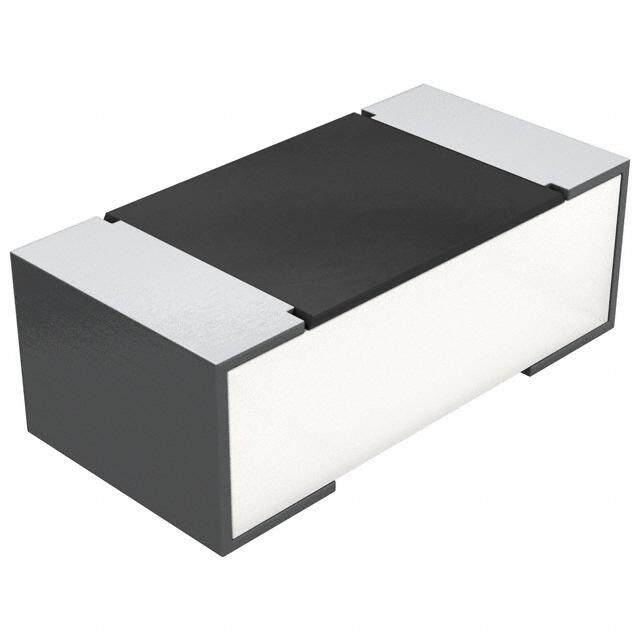
| 产品图片 |
|
| rohs | 符合RoHS无铅 / 符合限制有害物质指令(RoHS)规范要求 |
| 产品系列 | RF集成电路,射频接收器,Infineon Technologies TDK5110- |
| 数据手册 | http://www.infineon.com/dgdl/TDK5110_DS_V1.1.pdf?folderId=db3a30431689f4420116a096e1db033e&fileId=db3a3043191a246301192e318df72b6f |
| 产品型号 | TDK5110 |
| 产品种类 | 射频接收器 |
| 其它名称 | SP000013532 |
| 功率-输出 | 11dBm |
| 包装 | 带卷 (TR) |
| 商标 | Infineon Technologies |
| 天线连接器 | PCB,表面贴装 |
| 存储容量 | - |
| 安装风格 | SMD/SMT |
| 封装 | Reel |
| 封装/外壳 | 16-TSSOP(0.173",4.40mm 宽) |
| 封装/箱体 | TSSOP-16 |
| 工作温度 | -40°C ~ 125°C |
| 工作电源电压 | 2.5 V, 3.3 V |
| 工作频率 | 870 MHz |
| 工厂包装数量 | 3000 |
| 应用 | 遥控,RKE,安全系统 |
| 数据接口 | PCB,表面贴装 |
| 数据速率(最大值) | 20 kbps |
| 最大工作温度 | + 125 C |
| 最小工作温度 | - 40 C |
| 标准包装 | 3,000 |
| 特性 | - |
| 电压-电源 | 2.1 V ~ 4 V |
| 电流-传输 | 15.7mA |
| 类型 | Transmitter |
| 系列 | TDx5110 |
| 调制或协议 | ASK,FSK |
| 零件号别名 | SP000013532 TDK5110XUMA1 |
| 频率 | 433 ~ 435MHz; 866 ~ 870MHz |


- 商务部:美国ITC正式对集成电路等产品启动337调查
- 曝三星4nm工艺存在良率问题 高通将骁龙8 Gen1或转产台积电
- 太阳诱电将投资9.5亿元在常州建新厂生产MLCC 预计2023年完工
- 英特尔发布欧洲新工厂建设计划 深化IDM 2.0 战略
- 台积电先进制程称霸业界 有大客户加持明年业绩稳了
- 达到5530亿美元!SIA预计今年全球半导体销售额将创下新高
- 英特尔拟将自动驾驶子公司Mobileye上市 估值或超500亿美元
- 三星加码芯片和SET,合并消费电子和移动部门,撤换高东真等 CEO
- 三星电子宣布重大人事变动 还合并消费电子和移动部门
- 海关总署:前11个月进口集成电路产品价值2.52万亿元 增长14.8%


PDF Datasheet 数据手册内容提取
Wireless Components ASK/FSK Transmitter 868/433 MHz TDK 5110 Version 1.1 Specification October 2002 Preliminary
Revision History Current Version: Version 1.1 as of 31.10.2002 Previous Version: 1.0 as of March 2002 Page Page Subjects (major changes since last revision) (in previous (in current Version) Version) 5-4, 5-7 5-4, 5-7 Tolerances of Lcosc specified Value of Iclkout corrected ABM®, AOP®, ARCOFI®, ARCOFI®-BA, ARCOFI®-SP, DigiTape®, EPIC®-1, EPIC®-S, ELIC®, FALC®54, FALC®56, FALC®-E1, FALC®-LH, IDEC®, IOM®, IOM®-1, IOM®-2, IPAT®-2, ISAC®-P, ISAC®-S, ISAC®-S TE, ISAC®-P TE, ITAC®, IWE®, MUSAC®-A, OCTAT®-P, QUAT®-S, SICAT®, SICOFI®, SICOFI®- 2, SICOFI®-4, SICOFI®-4µC, SLICOFI® are registered trademarks of InfineonTechnologiesAG. Edition 31.10.2002 Published by Infineon Technologies AG, Balanstraße 73, 81541 München © InfineonTechnologiesAG 2002. All Rights Reserved. Attention please! As far as patents or other rights of third parties are concerned, liability is only assumed for components, not for applications, processes and circuits im- plemented within components or assemblies. The information describes the type of component and shall not be considered as assured characteristics. Terms of delivery and rights to change design reserved. Due to technical requirements components may contain dangerous substances. For information on the types in question please contact your nearest InfineonTechnologies Office. InfineonTechnologiesAG is an approved CECC manufacturer. Packing Please use the recycling operators known to you. We can also help you – get in touch with your nearest sales office. By agreement we will take packing material back, if it is sorted. You must bear the costs of transport. For packing material that is returned to us unsorted or which we are not obliged to accept, we shall have to invoice you for any costs incurred. Components used in life-support devices or systems must be expressly authorized for such purpose! Critical components1 of the InfineonTechnologiesAG, may only be used in life-support devices or systems2 with the express written approval of the InfineonTechnologiesAG. 1 A critical component is a component used in a life-support device or system whose failure can reasonably be expected to cause the failure of that life- support device or system, or to affect its safety or effectiveness of that device or system. 2 Life support devices or systems are intended (a) to be implanted in the human body, or (b) to support and/or maintain and sustain human life. If they fail, it is reasonable to assume that the health of the user may be endangered.
TDK 5110 Product Info Product Info General Description The TDK 5110 is a single chip ASK/ Package FSK transmitter for the frequency bands 868-870 MHz and 433-435 MHz. The IC offers a high level of inte- gration and needs only a few external components. The device contains a fully integrated PLL synthesizer and a high efficiency power amplifier to drive a loop antenna. A special circuit design and an unique power amplifier design are used to save current consumption and therefore to save battery life. Addi- tionally features like a power down mode, a low power detect, a selectable crystal oscillator frequency and a divided clock output are implemented. The IC can be used for both ASK and FSK modulation. Features (cid:1) fully integrated frequency synthe- (cid:1) voltage supply range 2.1 - 4 V sizer (cid:1) power down mode (cid:1) VCO without external components (cid:1) low voltage sensor (cid:1) high efficiency power amplifier (cid:1) selectable crystal oscillator typically 10 dBm @ 3 V 6.78 MHz/13.56 MHz (cid:1) switchable frequency range (cid:1) programmable divided clock output 868-870/433-435 MHz for µC (cid:1) ASK/FSK modulation (cid:1) low external component count (cid:1) low supply current typ. 13 mA@3V Applications (cid:1) Keyless entry systems (cid:1) Alarm systems (cid:1) Remote control systems (cid:1) Communication systems Ordering Information Type Ordering Code Package TDK 5110 Q67036-A1177 P-TSSOP-16 available on tape and reel Wireless Components Product Info Specification, October 2002
2 Product Description Contents of this Chapter 2.1 Overview. . . . . . . . . . . . . . . . . . . . . . . . . . . . . . . . . . . . . . . . . . . . . . .2-2 2.2 Applications . . . . . . . . . . . . . . . . . . . . . . . . . . . . . . . . . . . . . . . . . . . .2-2 2.3 Features . . . . . . . . . . . . . . . . . . . . . . . . . . . . . . . . . . . . . . . . . . . . . . .2-2 2.4 Package Outlines . . . . . . . . . . . . . . . . . . . . . . . . . . . . . . . . . . . . . . . .2-3
TDK 5110 Product Description 2.1 Overview The TDA5110 is a single chip ASK/FSK transmitter for the frequency bands 868-870 MHz and 433-435 MHz. The IC offers a high level of integration and needs only a few external components. The device contains a fully integrated PLL synthesizer and a high efficiency power amplifier to drive a loop antenna. A special circuit design and an unique power amplifier design are used to save current consumption and therefore to save battery life. Additional features like a power down mode, a low power detect, a selectable crystal oscillator fre- quency and a divided clock output are implemented. The IC can be used for both ASK and FSK modulation. 2.2 Applications (cid:1) Keyless entry systems (cid:1) Remote control systems (cid:1) Alarm systems (cid:1) Communication systems 2.3 Features (cid:1) fully integrated frequency synthesizer (cid:1) VCO without external components (cid:1) high efficiency power amplifier typ. 10 dBm @ 3 V (cid:1) switchable frequency range 868-870/433-435 MHz (cid:1) ASK/FSK modulation (cid:1) low supply current typ. 13 mA @ 3 V (cid:1) voltage supply range 2.1 - 4 V (cid:1) power down mode (cid:1) low voltage sensor (cid:1) selectable crystal oscillator 6.78 MHz/13.56 MHz (cid:1) programmable divided clock output for µC (cid:1) low external component count Wireless Components 2 - 2 Specification, October 2002
TDK 5110 Product Description 2.4 Package Outlines Figure 2-1 P-TSSOP-16 Wireless Components 2 - 3 Specification, October 2002
3 Functional Description Contents of this Chapter 3.1 Pin Configuration. . . . . . . . . . . . . . . . . . . . . . . . . . . . . . . . . . . . . . .3-2 3.2 Pin Definitions and Functions . . . . . . . . . . . . . . . . . . . . . . . . . . . . .3-3 3.3 Functional Block diagram . . . . . . . . . . . . . . . . . . . . . . . . . . . . . . . .3-7 3.4 Functional Blocks. . . . . . . . . . . . . . . . . . . . . . . . . . . . . . . . . . . . . . .3-8 3.4.1 PLL Synthesizer. . . . . . . . . . . . . . . . . . . . . . . . . . . . . . . . . . . . . . . .3-8 3.4.2 Crystal Oscillator . . . . . . . . . . . . . . . . . . . . . . . . . . . . . . . . . . . . . . .3-8 3.4.3 Power Amplifier . . . . . . . . . . . . . . . . . . . . . . . . . . . . . . . . . . . . . . . .3-9 3.4.4 Low Power Detect . . . . . . . . . . . . . . . . . . . . . . . . . . . . . . . . . . . . .3-10 3.4.5 Power Modes. . . . . . . . . . . . . . . . . . . . . . . . . . . . . . . . . . . . . . . . .3-10 3.4.5.1 Power Down Mode . . . . . . . . . . . . . . . . . . . . . . . . . . . . . . . . . . . .3-10 3.4.5.2 PLL Enable Mode . . . . . . . . . . . . . . . . . . . . . . . . . . . . . . . . . . . . .3-10 3.4.5.3 Transmit Mode. . . . . . . . . . . . . . . . . . . . . . . . . . . . . . . . . . . . . . . .3-10 3.4.6 Recommended timing diagrams for ASK- and FSK-Modulation . .3-12
TDK 5110 Functional Description 3.1 Pin Configuration PDWN 1 16 CSEL LPD 2 15 FSEL VS 3 14 PAOUT LF 4 13 PAGND TDK 5110 GND 5 12 FSKGND ASKDTA 6 11 FSKOUT FSKDTA 7 10 COSC CLKOUT 8 9 CLKDIV Pin_config.wmf Figure 3-1 IC Pin Configuration Table 3-1 Pin No. Symbol Function 1 PDWN Power Down Mode Control 2 LPD Low Power Detect Output 3 VS Voltage Supply 4 LF Loop Filter 5 GND Ground 6 ASKDTA Amplitude Shift Keying Data Input 7 FSKDTA Frequency Shift Keying Data Input 8 CLKOUT Clock Driver Output 9 CLKDIV Clock Divider Control 10 COSC Crystal Oscillator Input 11 FSKOUT Frequency Shift Keying Switch Output 12 FSKGND Frequency Shift Keying Ground 13 PAGND Power Amplifier Ground 14 PAOUT Power Amplifier Output 15 FSEL Frequency Range Selection (433 or 868 MHz) 16 CSEL Crystal Frequency Selection (6.78 or 13.56 MHz) Wireless Components 3 - 2 Specification, October 2002
TDK 5110 Functional Description 3.2 Pin Definitions and Functions Table 3-2 Pin Symbol Interface Schematic1) Function No. 1 PDWN Disable pin for the complete transmitter cir- V cuit. S 40 µA ∗ (ASKDTA+FSKDTA) A logic low (PDWN < 0.7 V) turns off all transmitter functions. 5 kΩ A logic high (PDWN > 1.5 V) gives access to 1 all transmitter functions. "ON" PDWN input will be pulled up by 40 µA inter- 150 kΩ nally by either setting FSKDTA or ASKDTA to a logic high-state. 250 kΩ 2 LPD This pin provides an output indicating the low-voltage state of the supply voltage VS. V S VS < 2.15 V will set LPD to the low-state. 40 µA An internal pull-up current of 40 µA gives the 2 output a high-state at supply voltages above 2.15 V. 300 Ω 3 VS This pin is the positive supply of the trans- mitter electronics. An RF bypass capacitor should be con- nected directly to this pin and returned to GND (pin 5) as short as possible. Wireless Components 3 - 3 Specification, October 2002
TDK 5110 Functional Description 4 LF Output of the charge pump and input of the V VCO control voltage. S The loop bandwidth of the PLL is 150 kHz when only the internal loop filter is used. 140 pF The loop bandwidth may be reduced by applying an external RC network referencing 15 pF to the positive supply VS (pin 3). 35 kΩ 10 kΩ 4 5 GND General ground connection. 6 ASKDTA Digital amplitude modulation can be +1.2 V imparted to the Power Amplifier through this pin. 60 kΩ A logic high (ASKDTA > 1.5 V or open) 6 enables the Power Amplifier. +1.1 V 90 kΩ A logic low (ASKDTA < 0.5 V) disables the Power Amplifier. 50 pF 30 µA 7 FSKDTA Digital frequency modulation can be +1.2 V imparted to the Xtal Oscillator by this pin. The VCO-frequency varies in accordance to the frequency of the reference oscillator. 60 kΩ 7 A logic high (FSKDTA > 1.5V or open) +1.1 V sets the FSK switch to a high impedance 90 kΩ state. 30 µA A logic low (FSKDTA < 0.5 V) closes the FSK switch from FSKOUT (pin 11) to FSKGND (pin 12). A capacitor can be switched to the reference crystal network this way. The Xtal Oscillator frequency will be shifted giving the designed FSK frequency deviation. Wireless Components 3 - 4 Specification, October 2002
TDK 5110 Functional Description 8 CLKOUT Clock output to supply an external device. An external pull-up resistor has to be added 8 in accordance to the driving requirements of 300 Ω the external device. A clock frequency of 3.39 MHz is selected by a logic low at CLKDIV input (pin 9). A clock frequency of 847.5 kHz is selected by a logic high at CLKDIV input (pin 9). 9 CLKDIV This pin is used to select the desired clock division rate for the CLKOUT signal. V S +1.2 V A logic low (CLKDIV < 0.2 V) applied to this pin selects the 3.39 MHz output signal at 5 µA CLKOUT (pin 8). 60 kΩ A logic high (CLKDIV open) applied to this 9 pin selects the 847.5 kHz output signal at +0.8 V CLKOUT (pin 8). 60 kΩ 10 COSC This pin is connected to the reference oscil- lator circuit. V S The reference oscillator is working as a neg- ative impedance converter. It presents a 6 kΩ negative resistance in series to an induc- tance at the COSC pin. 10 100 µA 11 FSKOUT This pin is connected to a switch to FSKGND (pin 12). V S The switch is closed when the signal at FSKDTA (pin 7) is in a logic low state. 200 µA The switch is open when the signal at FSKDTA (pin 7) is in a logic high state. 1.5 kΩ 11 FSKOUT can switch an additional capacitor to the reference crystal network to pull the crystal frequency by an amount resulting in 12 the desired FSK frequency shift of the trans- mitter output frequency. 12 FSKGND Ground connection for FSK modulation out- put FSKOUT. Wireless Components 3 - 5 Specification, October 2002
TDK 5110 Functional Description 13 PAGND Ground connection of the power amplifier. The RF ground return path of the power amplifier output PAOUT (pin 14) has to be concentrated to this pin. 14 PAOUT RF output pin of the transmitter. 14 A DC path to the positive supply VS has to be supplied by the antenna matching net- work. 13 15 FSEL This pin is used to select the desired trans- mitter frequency. +1.2 V A logic low (FSEL < 0.5 V) applied to this pin sets the transmitter to the 433 MHz fre- 30 kΩ quency range. 15 +1.1 V 90 kΩ A logic high (FSEL open) applied to this pin sets the transmitter to the 868 MHz fre- 30 µA quency range. 16 CSEL This pin is used to select the desired refer- ence frequency. V S +1.2 V A logic low (CSEL < 0.2 V) applied to this pin 5 µA sets the internal frequency divider to accept 60 kΩ a reference frequency of 6.78 MHz. 16 +0.8 V A logic high (CSEL open) applied to this pin 60 kΩ sets the internal frequency divider to accept a reference frequency of 13.56 MHz. 1) Indicated voltages and currents apply for PLL Enable Mode and Transmit Mode. In Power Down Mode, the values are zero or high-ohmic. Wireless Components 3 - 6 Specification, October 2002
W ir e le s s C o m p o n e n ts 3 . 3 FSK ASK Power Positive Low Power Data Data Down Supply F Detect Output F ig Input Input Control VS u u re 7 6 1 3 2 n 3 c -2 ti o FSK 12 n Fu Ground OR Power Low Voltage a n Supply Sensor 2.2V l ctio FSK 11 B na Switch On lo 3 - 7 l Block d 6.78/C1r3y.s5t6a lMHz 10 XOTsAcL PFD :128/64 VCO :1/2 PAoMwPer 14 PAOomuwtppeluifrtier ck di ia a g g ra r m 13 Power a Amplifier m Clock Output Frequency :2/8 LF Ground Select :4/16 9 0.85/3.39 MHz 8 16 4 15 5 Spec OCulotpcukt CSreylsetcatl LFoiltoepr FreSqeuleecntcy Ground Fun ifica 6.78/13.56 MHz 434/868 MHz ctio tio n n a , O l D T c e D tober 2002 Block_diagram.wm scription K 5110 f
TDK 5110 Functional Description 3.4 Functional Blocks 3.4.1 PLL Synthesizer The Phase Locked Loop synthesizer consists of a Voltage Controlled Oscillator (VCO), an asynchronous divider chain, a phase detector, a charge pump and a loop filter. It is fully implemented on chip. The tuning circuit of the VCO consist- ing of spiral inductors and varactor diodes is on chip, too. Therefore no addi- tional external components are necessary. The nominal center frequency of the VCO is 869 MHz. The oscillator signal is fed both, to the synthesizer divider chain and to the power amplifier. The overall division ratio of the asynchronous divider chain is 128 in case of a 6.78 MHz crystal or 64 in case of a 13.56 MHz crystal and can be selected via CSEL (pin 16). The phase detector is a Type IV PD with charge pump. The passive loop filter is realized on chip. 3.4.2 Crystal Oscillator The crystal oscillator operates either at 6.78 MHz or at 13.56 MHz. The reference frequency can be chosen by the signal at CSEL (pin 16). Table 3-3 CSEL (pin 16) Crystal Frequency Low1) 6.78 MHz Open2) 13.56 MHz 1) Low: Voltage at pin < 0.2 V 2) Open: Pin open For both quartz frequency options, 847.5 kHz or 3.39 MHz are available as out- put frequencies of the clock output CLKOUT (pin 8) to drive the clock input of a micro controller. The frequency at CLKOUT (pin 8) is controlled by the signal at CLKDIV (pin 9) Table 3-4 CLKDIV (pin 9) CLKOUT Frequency Low1) 3.39 MHz Open2) 847.5 kHz 1) Low: Voltage at pin < 0.2 V 2) Open: Pin open Wireless Components 3 - 8 Specification, October 2002
TDK 5110 Functional Description To achieve FSK transmission, the oscillator frequency can be detuned by a fixed amount by switching an external capacitor via FSKOUT (pin 11). The condition of the switch is controlled by the signal at FSKDTA (pin 7). Table 3-5 FSKDTA (pin7) FSK Switch Low1) CLOSED Open2), High3) OPEN 1) Low: Voltage at pin < 0.5 V 2) Open: Pin open 3) High: Voltage at pin > 1.5 V 3.4.3 Power Amplifier In case of operation in the 868-870 MHz band, the power amplifier is fed directly from the voltage controlled oscillator. In case of operation in the 433-435 MHz band, the VCO frequency is divided by 2. This is controlled by FSEL (pin 15) as described in the table below. Table 3-6 FSEL (pin 15) Radiated Frequency Band Low1) 433 MHz Open2) 868 MHz 1) Low: Voltage at pin < 0.5 V 2) Open: Pin open The Power Amplifier can be switched on and off by the signal at ASKDTA (pin 6). Table 3-7 ASKDTA (pin 6) Power Amplifier Low1) OFF Open2), High3) ON 1) Low: Voltage at pin < 0.5 V 2) Open: Pin open 3) High: Voltage at pin > 1.5 V The Power Amplifier has an Open Collector output at PAOUT (pin 14) and requires an external pull-up coil to provide bias. The coil is part of the tuning and matching LC circuitry to get best performance with the external loop antenna. To achieve the best power amplifier efficiency, the high frequency voltage swing at PAOUT (pin 14) should be twice the supply voltage. The power amplifier has its own ground pin PAGND (pin 13) in order to reduce the amount of coupling to the other circuits. Wireless Components 3 - 9 Specification, October 2002
TDK 5110 Functional Description 3.4.4 Low Power Detect The supply voltage is sensed by a low power detector. When the supply voltage drops below 2.15 V, the output LPD (pin 2) switches to the low-state. To mini- mize the external component count, an internal pull-up current of 40 µA gives the output a high-state at supply voltages above 2.15 V. The output LPD (pin 2) can either be connected to ASKDTA (pin 6) to switch off the PA as soon as the supply voltage drops below 2.15 V or it can be used to inform a micro-controller to stop the transmission after the current data packet. 3.4.5 Power Modes The IC provides three power modes, the POWER DOWN MODE, the PLL ENABLE MODE and the TRANSMIT MODE. 3.4.5.1 Power Down Mo de In the POWER DOWN MODE the complete chip is switched off. The current consumption is typically 0.25 nA at 3 V 25°C. This current doubles every 8°C. The values for higher temperatures are typically 14 nA at 85°C and typically 600 nA at 125°C. 3.4.5.2 PLL Enable Mode In the PLL ENABLE MODE the PLL is switched on but the power amplifier is turned off to avoid undesired power radiation during the time the PLL needs to settle. The turn on time of the PLL is determined mainly by the turn on time of the crystal oscillator and is less than 1 msec when the specified crystal is used. The current consumption is typically 4 mA. 3.4.5.3 Transmit Mode In the TRANSMIT MODE the PLL is switched on and the power amplifier is turned on too. The current consumption of the IC is typically 13 mA when using a proper trans- forming network at PAOUT, see Figure 4-1. 3.4.5.4 Power mode control The bias circuitry is powered up via a voltage V > 1.5 V at the pin PDWN (pin 1). When the bias circuitry is powered up, the pins ASKDTA and FSKDTA are pulled up internally. Forcing the voltage at the pins low overrides the internally set state. Wireless Components 3 - 10 Specification, October 2002
TDK 5110 Functional Description Alternatively, if the voltage at ASKDTA or FSKDTA is forced high externally, the PDWN pin is pulled up internally via a current source. In this case, it is not nec- essary to connect the PDWN pin, it is recommended to leave it open. The principle schematic of the power mode control circuitry is shown in Figure 3-5. PDWN ASKDTA OR FSKDTA On Bias Source 120 kΩ e g a Volt 120 kΩ FSKOUT s FSK a On Bi 868 PLL PA PAOUT MHz IC Power_Mode.wmf Figure 3-5 Power mode control circuitry Table 3-8 provides a listing of how to get into the different power modes Table 3-8 PDWN FSKDTA ASKDTA MODE Low1) Low, Open Low, Open POWER DOWN Open2) Low Low High3) Low, Open, High Low PLL ENABLE Open High Low High Low, Open, High Open, High Open High Open, High TRANSMIT Open Low, Open, High High 1) Low: Voltage at pin < 0.7 V (PDWN) Voltage at pin < 0.5 V (FSKDTA, ASKDTA) 2) Open: Pin open 3) High: Voltage at pin > 1.5 V Wireless Components 3 - 11 Specification, October 2002
TDK 5110 Functional Description Other combinations of the control pins PDWN, FSKDTA and ASKDTA are not recommended. 3.4.6 Recommended timing diagrams for ASK- and FSK-Modulation ASK Modulation using FSKDTA and ASKDTA, PDWN not connected Modes: Power Down PLL Enable Transmit High FSKDTA Low to t DATA Open, High ASKDTA Low to t min. 1 msec. ASK_mod.wmf Figure 3-6 ASK Modulation Wireless Components 3 - 12 Specification, October 2002
TDK 5110 Functional Description FSK Modulation using FSKDTA and ASKDTA, PDWN not connected Modes: Power Down PLL Enable Transmit DATA High FSKDTA Low to t High ASKDTA Low to t min. 1 msec. FSK_mod.wmf Figure 3-7 FSK Modulation Alternative ASK Modulation, FSKDTA not connected. Modes: Power Down PLL Enable Transmit High PDWN Low to t DATA Open, High ASKDTA Low to t min. 1 msec. Alt_ASK_mod.wmf Figure 3-8 Alternative ASK Modulation Wireless Components 3 - 13 Specification, October 2002
TDK 5110 Functional Description Alternative FSK Modulation Modes: Power Down PLL Enable Transmit High PDWN Low to t Open, High ASKDTA Low to t DATA Open, High FSKDTA Low to t min. 1 msec. Alt_FSK_mod.wmf Figure 3-9 Alternative FSK Modulation Wireless Components 3 - 14 Specification, October 2002
4 Applications Contents of this Chapter 4.1 50 Ohm-Output Testboard: Schematic. . . . . . . . . . . . . . . . . . . . . . . .4-2 4.2 50 Ohm-Output Testboard: Layout. . . . . . . . . . . . . . . . . . . . . . . . . . .4-3 4.3 50 Ohm-Output Testboard: Bill of material. . . . . . . . . . . . . . . . . . . . .4-4 4.4 50 Ohm-Output Testboard: Measurement results . . . . . . . . . . . . . . .4-5 4.5 Application Hints on the Crystal Oscillator . . . . . . . . . . . . . . . . . . . . .4-7 4.6 Design hints on the buffered clock output (CLKOUT). . . . . . . . . . . . .4-9 4.7 Application Hints on the Power-Amplifier . . . . . . . . . . . . . . . . . . . . .4-10
TDK 5110 Applications 4.1 50 Ohm-Output Testboard: Schematic X2SMA C8 C2 C4 L2 L1 VCC C7 433 (868) MHz C3 C6 Q1 0.85 (3.4) 6.78 (13.56) 16 15 14 13 12 11 10 9 MHz MHz TDK5110 1 2 3 4 5 6 7 8 C1 C C V T1 R3A VCC R3F R4 R2 ASK FSK C5 R1 X1SMA 50ohm_test_v5.wmf Figure 4-1 50Ω-output testboard schematic Wireless Components 4 - 2 Specification, October 2002
TDK 5110 Applications 4.2 50 Ohm-Output Testboard: Layout tda5110_v1_pcboben.pdf Figure 4-2 Top Side of TDK 5110-Testboard with 50 Ω-Output tda5110_v1_pcbunten.pdf Figure 4-3 Bottom Side of TDK 5110-Testboard with 50 Ω-Output Wireless Components 4 - 3 Specification, October 2002
TDK 5110 Applications 4.3 50 Ohm-Output Testboard: Bill of material Table 4-1 Bill of material Part Value 434 MHz 869 MHz ASK FSK Specification R1 4.7k 0805, ± 5% R2 12k 0805, ± 5% R3A 15k 0805, ± 5% R3F 15k 0805, ± 5% R4 open 0805, ± 5% C1 47nF 0805, X7R, ± 10% C2 27pF 27pF 0805, COG, ± 5% C3 6.8pF 2.7pF 0805, COG, ± 0.1 pF C4 330pF 100pF 0805, COG, ± 5% C5 1nF 0805, X7R, ± 10% C6 6.8pF 434MHz: 10pF 0805, COG, ± 0.1 pF 868MHz: 8.2pF C7 0Ω 6.8pF: 0805, COG, ± 0.1pF 434MHz: 6.8pF Jumper 15pF: 0805, COG, ± 1% 868MHz: 15pF 0805, 0Ω Jumper C8 12pF 5.6pF 5.6pF: 0805, COG, ± 0.1pF 12pF: 0805, COG, ± 1% L1 68nH 68nH TOKO LL2012-J L2 27nH 10nH 27nH: TOKO LL1608-J 10nH: TOKO PTL2012-J Q1 13.56875 MHz, Tokyo Denpa TSS-3B CL=20pF 13568.75 kHz Spec.No. 10-50205 IC1 TDK5110 T1 Push-button replaced by a short X1 SMA-S SMA standing X2 SMA-S SMA standing Wireless Components 4 - 4 Specification, October 2002
TDK 5110 Applications 4.4 50 Ohm-Output Testboard: Measurement results Note the specified operating range: 2.1 V to 4.0 V and −40°C to +125°C. Pout over temperature TDK5110 434 MHz 14,00 12,00 10,00 4,0V ] m 3,0V B 8,00 d 2,1V out [ 6,00 2,0V P 4,00 1,9V 2,00 0,00 -50 0 50 100 150 T [°C] pout_over_temp_434.wmf Figure 4-4 Pout over temperature of the 50Ω-testboard with TDK5110 at 434 MHz Is over temperature TDK5110 434 MHz 18,00 16,00 4,0V 14,00 3,0V ] A m 12,00 2,1V [ s 2,0V I 10,00 1,9V 8,00 6,00 -50 0 50 100 150 T [°C] is_over_temp_434.wmf Figure 4-5 Is over temperature of the 50Ω-testboard with TDK5110 at 434 MHz Wireless Components 4 - 5 Specification, October 2002
TDK 5110 Applications Note the specified operating range: 2.1 V to 4.0 V and −40°C to +125°C. Pout over temperature TDK5110 868 MHz 14,00 12,00 10,00 4,0V m] 3,0V B 8,00 d 2,1V ut [ 6,00 2,0V o P 4,00 1,9V 2,00 0,00 -50 0 50 100 150 T [°C] pout_over_temp_868.wmf Figure 4-6 Pout over temperature of the 50Ω-testboard with TDK5110 at 868 MHz Is over temperature TDK5110 868 MHz 18,00 16,00 4,0V 14,00 3,0V ] A m 12,00 2,1V [ s 2,0V I 10,00 1,9V 8,00 6,00 -50 0 50 100 150 T [°C] is_over_temp_868.wmf Figure 4-7 Is over temperature of the 50Ω-testboard with TDK5110 at 868 MHz Wireless Components 4 - 6 Specification, October 2002
TDK 5110 Applications 4.5 Application Hints on the Crystal Oscillator The crystal oscillator achieves a turn on time less than 1 msec when the specified crystal is used. To achieve this, a NIC oscillator type is implemented in the TDK 5110. The input impedance of this oscillator is a negative resistance in series to an inductance. Therefore the load capacitance of the crystal CL (specified by the crystal supplier) is transformed to the capacitance Cv. -R L f, CL Cv TDK 5110 1 Cv = (1) 1 +ω2L CL CL: crystal load capacitance for nominal frequency ω: angular frequency L: inductance of the crystal oscillator Example for the ASK-Mode: Referring to the application circuit, in ASK-Mode the capacitance C7 is replaced by a short to ground. Assume a crystal frequency of 13.56 MHz and a crystal load capacitance of CL = 20 pF. The inductance L at 13.5 MHz is about 4.6 µH. Therefore C6 is calculated to 12 pF. 1 Cv= =C6 1 +ω2L CL Wireless Components 4 - 7 Specification, October 2002
TDK 5110 Applications Example for the FSK-Mode: FSK modulation is achieved by switching the load capacitance of the crystal as shown below. FSKDTA FSKOUT Csw -R L f, CL Cv1 Cv2 COSC IC The frequency deviation of the crystal oscillator is multiplied with the divider factor N of the Phase Locked Loop to the output of the power amplifier. In case of small frequency deviations (up to +/- 1000 ppm), the two desired load capacitances can be calculated with the formula below. ∆f 2(C0+CL) CL(cid:1)C0 (1+ ) N* f1 C1 CL± = ∆f 2(C0+CL) 1± (1+ ) N* f1 C1 C : crystal load capacitance for nominal frequency L C : shunt capacitance of the crystal 0 f: frequency ω: ω = 2πf: angular frequency N: division ratio of the PLL df: peak frequency deviation Because of the inductive part of the TDK 5110, these values must be corrected by Formula 1). The value of Cv± can be calculated. Wireless Components 4 - 8 Specification, October 2002
TDK 5110 Applications If the FSK switch is closed, Cv_ is equal to Cv1 (C6 in the application diagram). If the FSK switch is open, Cv2 (C7 in the application diagram) can be calculated. Csw∗Cv1−(Cv+)∗(Cv1+Csw) Cv2=C7= (Cv+)−Cv1 Csw: parallel capacitance of the FSK switch (3 pF incl. layout parasitics) Remark: These calculations are only approximations. The necessary values depend on the layout also and must be adapted for the specific application board. The 434 MHz 50Ω-Output testboard shows an FSK-deviation of +/- 24 kHz, typically. The 868 MHz 50Ω-Output testboard shows an FSK-deviation of +/- 27 kHz, typically. 4.6 Design hints on the buffered clock output (CLKOUT) The CLKOUT pin is an open collector output. An external pull up resistor (RL) should be connected between this pin and the positive supply voltage. The value of RL is depending on the clock frequency and the load capacitance CLD (PCB board plus input capacitance of the microcontroller). RL can be calculated to: 1 RL= fCLKOUT*8*CLD Table 4-2 fCLKOUT= fCLKOUT= 847 kHz 3.39 MHz CL[pF] RL[kΩ] CL[pF] RL[kΩ] 5 27 5 6.8 10 12 10 3.3 20 6.8 20 1.8 Remark: To achieve a low current consumption and a low spurious radiation, the largest possible RL should be chosen. Wireless Components 4 - 9 Specification, October 2002
TDK 5110 Applications 4.7 Application Hints on the Power-Amplifier The power amplifier operates in a high efficient class C mode. This mode is characterized by a pulsed operation of the power amplifier transistor at a current flow angle of θ<<π. A frequency selective network at the amplifier output passes the fundamental frequency component of the pulse spectrum of the collector current to the load. The load and its resonance transformation to the collector of the power amplifier can be generalized by the equivalent circuit of Figure 4-8. The tank circuit L//C//RL in parallel to the output impedance of the transistor should be in resonance at the operating frequency of the transmitter. V S L C R L Equivalent_power_wmf. Figure 4-8 Equivalent power amplifier tank circuit The optimum load at the collector of the power amplifier for “critical” operation under idealized conditions at resonance is: V 2 = R S LC 2P O A typical value of R for an RF output power of P = 10 mW is: LC o 32 = = Ω R 450 LC 2∗0.01 “Critical” operation is characterized by the RF peak voltage swing at the collector of the PA transistor to just reach the supply voltage V . S The high degree of efficiency under “critical” operating conditions can be explained by the low power losses at the transistor. During the conducting phase of the transistor, its collector voltage is very small. This way the power loss of the transistor, equal to i *u , is minimized. This is particularly true for C CE small current flow angles of θ<<π. In practice the RF-saturation voltage of the PA transistor and other parasitics reduce the “critical” R . LC Wireless Components 4 - 10 Specification, October 2002
TDK 5110 Applications The output power P is reduced by operating in an “overcritical” mode o characterised by R > R . L LC The power efficiency (and the bandwidth) increase when operating at a slightly higher R , as shown in Figure 4-9. L The collector efficiency E is defined as P = E O V I S C The diagram of Figure 4-9 was measured directly at the PA-output at V = 3 V. S Losses in the matching circuitry decrease the output power by about 1.5 dB. As can be seen from the diagram, 250 Ω is the optimum impedance for operation at 3 V. For an approximation of R and P at other supply voltages those OPT OUT two formulas can be used: R ~V OPT S and P ~ R OUT OPT 18 16 14 12 10 Pout [mW] 8 10*Ec 6 4 2 0 0 100 200 300 400 500 RL [Ohm] Power_E_vs_RL.wmf Figure 4-9 Output power P (mW) and collector efficiency E vs. load resistor R . o L The DC collector current I of the power amplifier and the RF output power P c o vary with the load resistor R . This is typical for overcritical operation of class C L amplifiers. The collector current will show a characteristic dip at the resonance frequency for this type of “overcritical” operation. The depth of this dip will increase with higher values of R . L Wireless Components 4 - 11 Specification, October 2002
TDK 5110 Applications As Figure 4-10 shows, detuning beyond the bandwidth of the matching circuit results in an increase of the collector current of the power amplifier and in some loss of output power. This diagram shows the data for the circuit of the test board at the frequency of 434 MHz. The behaviour at 868 MHz is similar. The effective load resistance of this circuit is R = 250 Ω, which is the optimum L impedance for operation at 3 V. This will lead to a dip of the collector current of approx. 10%. 16 14 TDK5110 434 MHz / 3V 12 10 8 Is [mA] Pout [dBm] 6 4 2 0 375 400 425 450 475 500 f [MHz] pout_vs_frequ.wmf Figure 4-10 Output power and collector current vs. frequency C3, L2-C2 and C8 are the main matching components which are used to transform the 50 Ω load at the SMA-RF-connector to a higher impedance at the PA-output (250 Ω @ 3 V). L1 can be used for some finetuning of the resonant frequency but should not become too small in order to keep its losses low. The transformed impedance of 250+j0 Ω at the PA-output-pin can be verified with a network analyzer using the following measurement procedure: 1. Calibrate your network analyzer. 2. Connect some short, low-loss 50 Ω cable to your network analyzer with an open end on one side. Semirigid cable works best. 3. Use the „Port Extension“ feature of your network analyzer to shift the refer- ence plane of your network analyzer to the open end of the cable. 4. Connect the center-conductor of the cable to the solder pad of the pin „PA“ of the IC. The outer conductor has to be grounded. Very short connections have to be used. Do not remove the IC or any part of the matching-compo- nents! 5. Screw a 50 Ω dummy-load on the RF-I/O-SMA-connector 6. Be sure that your network analyzer is AC-coupled and turn on the power supply of the IC. The TDK5110 has to be in PLL-Enable-Mode. 7. Measure the S-parameter S11 Wireless Components 4 - 12 Specification, October 2002
TDK 5110 Applications Plot0.pcx Figure 4-11 Sparam_measured_200M Above you can see the measurement of the evalboard with a span of 200 MHz. The evalboard has been optimized for 3 V. The load is about 250+j0 Ω at the transmit frequency. A tuning-free realization requires a careful design of the components within the matching network. A simple linear CAE-tool will help to see the influence of tolerances of matching components. Suppression of spurious harmonics may require some additional filtering within the antenna matching circuit. The total spectrum of the 50 Ω-Output testboard can be summarized as: Table 4-3 Frequency Output Power Output Power 434 MHz Testboard 868 MHz Testboard Fundamental +10 dBm +10 dBm Fund − 13.56 MHz −75 dBc −61 dBc Fund + 13.56 MHz −69 dBc −63 dBc 2nd harmonic −45 dBc −54 dBc 3rd harmonic −77 dBc −56 dBc Wireless Components 4 - 13 Specification, October 2002
5 Reference Contents of this Chapter 5.1 Absolute Maximum Ratings . . . . . . . . . . . . . . . . . . . . . . . . . . . . . . . .5-2 5.2 Operating Range . . . . . . . . . . . . . . . . . . . . . . . . . . . . . . . . . . . . . . . .5-2 5.3.1 AC/DC Characteristics at 3V, 25°C . . . . . . . . . . . . . . . . . . . . . . . . . .5-3 5.3.2 AC/DC Characteristics at 2.1 V ... 4.0 V, -40°C ... +125°C. . . . . . . . .5-6
TDK 5110 Reference 5.1 Absolute Maximum Ratings The AC / DC characteristic limits are not guaranteed. The maximum ratings must not be exceeded under any circumstances, not even momentarily and individually, as permanent damage to the IC may result. Table 5-1 Parameter Symbol Limit Values Unit Remarks Min Max Junction Temperature T -40 150 °C J Storage Temperature T -40 125 °C s Thermal Resistance R 230 K/W thJA Voltage at any pin V -0.3 V + 0.3 V pins S excluding pin 14 Voltage at pin 14 V -0.3 2 * V V No ESD-Diode to V pin14 S S Current into pin 11 I -10 10 mA pin11 ESD integrity, all pins V -1 +1 kV JEDEC Standard ESD JESD22-A114-B ESD integrity, all pins V -2.5 +2.5 kV JEDEC Standard ESD excluding pin 11 and pin 14 JESD22-A114-B Ambient Temperature under bias: T = -40°C to +125°C A Note: All voltages referred to ground (pins) unless stated otherwise. Pins 5, 12 and 13 are grounded. 5.2 Operating Range Within the operating range the IC operates as described in the circuit descrip- tion. Table 5-2 Parameter Symbol Limit Values Unit Test Conditions Min Max Supply voltage V 2.1 4.0 V S Ambient temperature T -40 125 °C A Wireless Components 5 - 2 Specification, October 2002
TDK 5110 Reference 5.3 AC/DC Characteristics 5.3.1 AC/DC Characteristics at 3V, 25°C Table 5-3 Supply Voltage V = 3 V, Ambient temperature T = 25°C S amb Parameter Symbol Limit Values Unit Test Conditions Min Typ Max Current consumption Power-Down mode I 0.25 100 nA V (Pins 1, 6 and 7) S PDWN < 0.2 V PLL-Enable mode I 4 5 mA S PLL_EN Transmit mode I 13.8 16.5 mA Load tank see S TRANSM Figure 4-1 and 4-2 Power Down Mode Control (Pin 1) Stand-by mode V 0 0.7 V V < 0.2 V PDWN ASKDTA V < 0.2 V FSKDTA PLL enable mode V 1.5 V V V < 0.5 V PDWN S ASKDTA Transmit mode V 1.5 V V V > 1.5 V PDWN S ASKDTA Input bias current PDWN I 30 µA V = V PDWN PDWN S Low Power Detect Output (Pin 2) Internal pull up current I 30 µA V = 2.3 V ... V LPD1 S S Input current low voltage I 1 mA V = 1.9 V ... 2.1 V LPD2 S Loop Filter (Pin 4) VCO tuning voltage V V - 1.5 V - 0.7 V f = 867.84 MHz LF S S VCO Output frequency range f 854 869 884 MHz V = V OUT, 868 FSEL S 868 MHz-band f f OUT = VCO Output frequency range f 427 434.5 442 MHz V = 0 V OUT, 433 FSEL 433 MHz-band f f / 2 OUT = VCO ASK Modulation Data Input (Pin 6) ASK Transmit disabled V 0 0.5 V ASKDTA ASK Transmit enabled V 1.5 V V ASKDTA S Input bias current ASKDTA I 30 µA V = V ASKDTA ASKDTA S Input bias current ASKDTA I -20 µA V = 0 V ASKDTA ASKDTA ASK data rate f 20 kHz ASKDTA Wireless Components 5 - 3 Specification, October 2002
TDK 5110 Reference Table 5-3 Supply Voltage V = 3 V, Ambient temperature T = 25°C S amb Parameter Symbol Limit Values Unit Test Conditions Min Typ Max FSK Modulation Data Input (Pin 7) FSK Switch on V 0 0.5 V FSKDTA FSK Switch off V 1.5 V V FSKDTA S Input bias current FSKDTA I 30 µA V = V FSKDTA FSKDTA S Input bias current FSKDTA I -20 µA V = 0 V FSKDTA FSKDTA FSK data rate f 20 kHz FSKDTA Clock Driver Output (Pin 8) Output current (High) I 5 µA V = V CLKOUT CLKOUT S Saturation Voltage (Low)1) VSATL 0.56 V ICLKOUT = 1 mA Clock Divider Control (Pin 9) Setting Clock Driver output V 0 0.2 V CLKDIV frequency f =3.39 MHz CLKOUT Setting Clock Driver output V V pin open CLKDIV frequency f =847.5kHz CLKOUT Input bias current CLKDIV I 30 µA V = V CLKDIV CLKDIV S Input bias current CLKDIV I -20 µA V = 0 V CLKDIV CLKDIV Crystal Oscillator Input (Pin 10) Load capacitance C 5 pF COSCmax Serial Resistance of the crys- 100 Ω f = 6.78 MHz tal Input inductance of the 3.25 4.25 5.25 µH f = 6.78 MHz COSC pin Serial Resistance of the crys- 100 Ω f = 13.56 MHz tal Input inductance of the 3.6 4.6 5.6 µH f = 13.56 MHz COSC pin FSK Switch Output (Pin 11) On resistance R 250 Ω V = 0 V FSKOUT FSKDTA On capacitance C 6 pF V = 0 V FSKOUT FSKDTA Off resistance R 10 kΩ V = V FSKOUT FSKDTA S Off capacitance C 1.5 pF V = V FSKOUT FSKDTA S Wireless Components 5 - 4 Specification, October 2002
TDK 5110 Reference Table 5-3 Supply Voltage V = 3 V, Ambient temperature T = 25°C S amb Parameter Symbol Limit Values Unit Test Conditions Min Typ Max Power Amplifier Output (Pin 14) Output Power2) POUT433 8 10 12 dBm fOUT = 433 MHz transformed to 50 Ohm V = 0 V FSEL P 8 10 12 dBm f = 868 MHz OUT868 OUT V = V FSEL S Frequency Range Selection (Pin 15) Transmit frequency 433 MHz V 0 0.5 V FSEL Transmit frequency 868 MHz V V pin open FSEL Input bias current FSEL I 25 µA V = V FSEL FSEL S Input bias current FSEL I -20 µA V = 0 V FSEL FSEL Crystal Frequency Selection (Pin 16) Crystal frequency 6.78 MHz VCSEL 0 0.2 V Crystal frequency 13.56 MHz V V pin open CSEL Input bias current CSEL I 50 µA V = V CSEL CSEL S Input bias current CSEL I -20 µA V = 0 V CSEL CSEL 1) Derating linearly to a saturation voltage of max. 140 mV at I = 0 mA CLKOUT 2) Power amplifier in overcritical C-operation Matching circuitry as used in the 50 Ohm-Output Testboard at the specified frequency. Tolerances of the passive elements not taken into account. Wireless Components 5 - 5 Specification, October 2002
TDK 5110 Reference 5.3.2 AC/DC Characteristics at 2.1 V ... 4.0 V, -40°C ... +125°C Table 5-4 Supply Voltage V = 2.1 V ... 4.0 V, Ambient temperature T = -40°C ... +125°C S amb Parameter Symbol Limit Values Unit Test Conditions Min Typ Max Current consumption Power-Down mode I 4 µA V (Pins 1, 6 and 7) S PDWN < 0.2 V PLL-Enable mode I 2.8 4 5.5 mA S PLL_EN Transmit mode I 10.8 14.5 mA V = 2.1 V S TRANSM S Load tank see I 13.8 17 mA V = 3.0 V Figure 4-1 and 4-2 S TRANSM S I 15.7 19 mA V = 4.0 V S TRANSM S Power Down Mode Control (Pin 1) Stand-by mode V 0 0.5 V V < 0.2 V PDWN ASKDTA V < 0.2 V FSKDTA PLL enable mode V 1.5 V V V < 0.5 V PDWN S ASKDTA Transmit mode V 1.5 V V V > 1.5 V PDWN S ASKDTA Input bias current PDWN I 38 µA V = V PDWN PDWN S Low Power Detect Output (Pin 2) Internal pull up current I 30 µA V = 2.3 V ... V LPD1 S S Input current low voltage I 0.5 mA V = 1.9 V ... 2.1 V LPD2 S Loop Filter (Pin 4) VCO tuning voltage V V - 1.8 V - 0.5 V f = 867.84 MHz LF S S VCO Output frequency range 1) fOUT, 868 864 869 874 MHz VFSEL = VS 868 MHz-band f f OUT = VCO Output frequency range f 432 434.5 437 MHz V = 0 V OUT, 433 FSEL 433 MHz-band f f / 2 OUT = VCO ASK Modulation Data Input (Pin 6) ASK Transmit disabled V 0 0.5 V ASKDTA ASK Transmit enabled V 1.5 V V ASKDTA S Input bias current ASKDTA I 33 µA V = V ASKDTA ASKDTA S Input bias current ASKDTA I -20 µA V = 0 V ASKDTA ASKDTA ASK data rate f 20 kHz ASKDTA Wireless Components 5 - 6 Specification, October 2002
TDK 5110 Reference Table 5-4 Supply Voltage V = 2.1 V ... 4.0 V, Ambient temperature T = -40°C ... +125°C S amb Parameter Symbol Limit Values Unit Test Conditions Min Typ Max FSK Modulation Data Input (Pin 7) FSK Switch on V 0 0.5 V FSKDTA FSK Switch off V 1.5 V V FSKDTA S Input bias current FSKDTA I 35 µA V = V FSKDTA FSKDTA S Input bias current FSKDTA I -20 µA V = 0 V FSKDTA FSKDTA FSK data rate f 20 kHz FSKDTA Clock Driver Output (Pin 8) Output current (High) I 5 µA V = V CLKOUT CLKOUT S Saturation Voltage (Low)2) VSATL 0.5 V ICLKOUT = 0.6 mA Clock Divider Control (Pin 9) Setting Clock Driver output V 0 0.2 V CLKDIV frequency f =3.39 MHz CLKOUT Setting Clock Driver output V V pin open CLKDIV frequency f =847.5kHz CLKOUT Input bias current CLKDIV I 30 µA V = V CLKDIV CLKDIV S Input bias current CLKDIV I -20 µA V = 0 V CLKDIV CLKDIV Crystal Oscillator Input (Pin 10) Load capacitance C 5 pF COSCmax Serial Resistance of the crys- 100 Ω f = 6.78 MHz tal Input inductance of the 2.9 4.25 6 µH f = 6.78 MHz COSC pin Serial Resistance of the crys- 100 Ω f = 13.56 MHz tal Input inductance of the 3.2 4.6 6.3 µH f = 13.56 MHz COSC pin FSK Switch Output (Pin 11) On resistance R 280 Ω V = 0 V FSKOUT FSKDTA On capacitance C 6 pF V = 0 V FSKOUT FSKDTA Off resistance R 10 kΩ V = V FSKOUT FSKDTA S Off capacitance C 1.5 pF V = V FSKOUT FSKDTA S Wireless Components 5 - 7 Specification, October 2002
TDK 5110 Reference Table 5-4 Supply Voltage V = 2.1 V ... 4.0 V, Ambient temperature T = -40°C ... +125°C S amb Parameter Symbol Limit Values Unit Test Conditions Min Typ Max Power Amplifier Output (Pin 14) Output Power3) at 433 MHz POUT, 433 5 6.5 8.5 dBm VS = 2.1 V transformed to 50 Ohm. P 7 10 12 dBm V = 3.0 V OUT, 433 S VFSEL = 0 V POUT, 433 7.5 11.5 13.5 dBm VS = 4.0 V Output Power4) at 868 MHz POUT, 868 5.8 7.5 8.5 dBm VS = 2.1 V transformed to 50 Ohm. P 7.1 10.2 12.2 dBm V = 3.0 V OUT, 868 S VFSEL = VS POUT, 868 7.5 11 12.5 dBm VS = 4.0 V Frequency Range Selection (Pin 15) Transmit frequency 433 MHz V 0 0.5 V FSEL Transmit frequency 868 MHz V V pin open FSEL Input bias current FSEL I 35 µA V = V FSEL FSEL S Input bias current FSEL I -20 µA V = 0 V FSEL FSEL Crystal Frequency Selection (Pin 16) Crystal frequency 6.78 MHz V 0 0.2 V CSEL Crystal frequency 13.56 MHz V V pin open CSEL Input bias current CSEL I 55 µA V = V CSEL CSEL S Input bias current CSEL I -25 µA V = 0 V CSEL CSEL 1) The output-frequency range can be increased by limiting the temperature and supply voltage range. Minimum f − 1 MHz => Minimum T + 5°C VCO amb Maximum f + 1 MHz => Maximum T − 5°C VCO amb Maximum f + 1 MHz => Minimum V + 25 mV, max. + 40 MHz. VCO S 2) Derating linearly to a saturation voltage of max. 140 mV at I = 0 mA CLKOUT 3) Matching circuitry as used in the 50 Ohm-Output Testboard for 434 MHz operation. Tolerances of the passive elements not taken into account. Range @ 2.1 V, +25°C: 6.5 dBm +/- 1 dBm Typ. temperature dependency at 2.1 V: -0.5 dBm@-40°C and -0.5 dBm@+125°C, reference +25°C. Range @ 3.0 V, +25°C: 10 dBm +/- 2.0 dBm Typ. temperature dependency at 3.0 V: -0.3 dBm@-40°C and -1.0 dBm@+125°C, reference +25°C. Range @ 4.0 V, +25°C: 11.5 dBm +/- 2.5 dBm Typ. temperature dependency at 4.0 V: -0.2 dBm@-40°C and -1.5 dBm@+125°C, reference +25°C. 4) Matching circuitry as used in the 50 Ohm-Output Testboard for 868 MHz operation. Tolerances of the passive elements not taken into account. Range @ 2.1 V, +25°C: 7.5 dBm +/- 1.0 dBm Typ. temperature dependency at 2.1 V: -0.2 dBm@-40°C and -0.7 dBm@+125°C, reference +25°C. Range @ 3.0 V, +25°C: 10.2 dBm +/- 2.0 dBm Typ. temperature dependency at 3.0 V: -0.5 dBm@-40°C and -1.1 dBm@+125°C, reference +25°C. Range @ 4.0 V, +25°C: 11 dBm +/- 2.5 dBm Typ. temperature dependency at 4.0 V: -0.9 dBm@-40°C and -1.0 dBm@+125°C, reference +25°C. A smaller load impedance reduces the supply-voltage dependency. A higher load impedance reduces the temperature dependency. Wireless Components 5 - 8 Specification, October 2002
Mouser Electronics Authorized Distributor Click to View Pricing, Inventory, Delivery & Lifecycle Information: I nfineon: TDK5110