ICGOO在线商城 > TDA7200
 Datasheet下载
- 型号: TDA7200
- 制造商: Infineon
- 库位|库存: xxxx|xxxx
- 要求:
| 数量阶梯 | 香港交货 | 国内含税 |
| +xxxx | $xxxx | ¥xxxx |
查看当月历史价格
查看今年历史价格
TDA7200产品简介:
ICGOO电子元器件商城为您提供TDA7200由Infineon设计生产,在icgoo商城现货销售,并且可以通过原厂、代理商等渠道进行代购。 提供TDA7200价格参考¥8.68-¥17.72以及InfineonTDA7200封装/规格参数等产品信息。 你可以下载TDA7200参考资料、Datasheet数据手册功能说明书, 资料中有TDA7200详细功能的应用电路图电压和使用方法及教程。
| 参数 | 数值 |
| 产品目录 | |
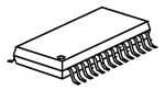
| 描述 | IC RECEIVER FSK/ASK 28-TSSOP射频接收器 ASK/FSK SNGL Convrsn Receiver |
| 产品分类 | |
| 品牌 | Infineon Technologies |
| 产品手册 | |
| 产品图片 |
|
| rohs | 符合RoHS无铅 / 符合限制有害物质指令(RoHS)规范要求 |
| 产品系列 | RF集成电路,射频接收器,Infineon Technologies TDA7200- |
| 数据手册 | http://www.infineon.com/dgdl/TDA7200_DS_V1.0.pdf?folderId=db3a30431689f4420116a096e1db033e&fileId=db3a3043191a24630119291a25ba7f9b |
| 产品型号 | TDA7200 |
| 产品种类 | 射频接收器 |
| 供应商器件封装 | PG-TSSOP-28 |
| 其它名称 | TDA7200INDKR |
| 包装 | Digi-Reel® |
| 商标 | Infineon Technologies |
| 天线连接器 | PCB,表面贴装 |
| 存储容量 | - |
| 安装风格 | SMD/SMT |
| 封装 | Reel |
| 封装/外壳 | 28-TSSOP(0.173",4.40mm 宽) |
| 封装/箱体 | TSSOP-28 |
| 工作温度 | -20°C ~ 70°C |
| 工作电源电压 | 5 V |
| 工作频率 | 440 MHz |
| 工厂包装数量 | 3000 |
| 带宽 | 440 MHz |
| 应用 | 远程传感器和触发器 |
| 数据接口 | PCB,表面贴装 |
| 数据速率(最大值) | 100 kbps |
| 最大工作温度 | + 70 C |
| 最小工作温度 | - 20 C |
| 标准包装 | 1 |
| 灵敏度 | -110dBm |
| 特性 | - |
| 电压-电源 | 4.5 V ~ 5.5 V |
| 电流-接收 | 5.7mA |
| 电源电压-最大 | 5.5 V |
| 电源电压-最小 | 4.5 V |
| 电源电流 | 7.7 mA |
| 类型 | Superheterodyne Receiver |
| 系列 | TDx7200 |
| 调制或协议 | ASK,FSK |
| 零件号别名 | SP000296473 TDA7200XUMA1 |
| 频率 | 400MHz ~ 440MHz |


- 商务部:美国ITC正式对集成电路等产品启动337调查
- 曝三星4nm工艺存在良率问题 高通将骁龙8 Gen1或转产台积电
- 太阳诱电将投资9.5亿元在常州建新厂生产MLCC 预计2023年完工
- 英特尔发布欧洲新工厂建设计划 深化IDM 2.0 战略
- 台积电先进制程称霸业界 有大客户加持明年业绩稳了
- 达到5530亿美元!SIA预计今年全球半导体销售额将创下新高
- 英特尔拟将自动驾驶子公司Mobileye上市 估值或超500亿美元
- 三星加码芯片和SET,合并消费电子和移动部门,撤换高东真等 CEO
- 三星电子宣布重大人事变动 还合并消费电子和移动部门
- 海关总署:前11个月进口集成电路产品价值2.52万亿元 增长14.8%


PDF Datasheet 数据手册内容提取
Data Sheet, V 1.0, May 2007 TDA7200 ASK/FSK Single Conversion Receiver Version 1.0 Wireless Control Components N e v e r s t o p t h i n k i n g .
Edition 2007-05-02 Published by Infineon Technologies AG, Am Campeon 1-12, 85579 Neubiberg, Germany © Infineon Technologies AG 2007-05-02. All Rights Reserved. Attention please! The information herein is given to describe certain components and shall not be considered as a guarantee of characteristics. Terms of delivery and rights to technical change reserved. We hereby disclaim any and all warranties, including but not limited to warranties of non-infringement, regarding circuits, descriptions and charts stated herein. Information For further information on technology, delivery terms and conditions and prices please contact your nearest Infineon Technologies Office in Germany or the Infineon Technologies Companies and our Infineon Technologies Representatives worldwide (www.infineon.com). Warnings Due to technical requirements components may contain dangerous substances. For information on the types in question please contact your nearest Infineon Technologies Office. Infineon Technologies Components may only be used in life-support devices or systems with the express written approval of Infineon Technologies, if a failure of such components can reasonably be expected to cause the failure of that life-support device or system, or to affect the safety or effectiveness of that device or system. Life support devices or systems are intended to be implanted in the human body, or to support and/or maintain and sustain and/or protect human life. If they fail, it is reasonable to assume that the health of the user or other persons may be endangered.
Data Sheet, V 1.0, May 2007 TDA7200 ASK/FSK Single Conversion Receiver Version 1.0 Wireless Control Components N e v e r s t o p t h i n k i n g .
TDA7200 Revision History: 2007-05-02 V 1.0 Previous Version: none Page Subjects (major changes since last revision) We Listen to Your Comments Any information within this document that you feel is wrong, unclear or missing at all? Your feedback will help us to continuously improve the quality of this document. Please send your proposal (including a reference to this document) to: sensors@infineon.com
TDA7200 Table of Contents Page 1 Product Description . . . . . . . . . . . . . . . . . . . . . . . . . . . . . . . . . . . . . . . . . 6 1.1 Overview . . . . . . . . . . . . . . . . . . . . . . . . . . . . . . . . . . . . . . . . . . . . . . . . . . . 6 1.2 Features . . . . . . . . . . . . . . . . . . . . . . . . . . . . . . . . . . . . . . . . . . . . . . . . . . . . 6 1.3 Application . . . . . . . . . . . . . . . . . . . . . . . . . . . . . . . . . . . . . . . . . . . . . . . . . . 6 2 Functional Description . . . . . . . . . . . . . . . . . . . . . . . . . . . . . . . . . . . . . . . 7 2.1 Pin Configuration . . . . . . . . . . . . . . . . . . . . . . . . . . . . . . . . . . . . . . . . . . . . . 7 2.2 Pin Definition and Functions . . . . . . . . . . . . . . . . . . . . . . . . . . . . . . . . . . . . 8 2.3 Functional Block Diagram . . . . . . . . . . . . . . . . . . . . . . . . . . . . . . . . . . . . . 15 2.4 Functional Block Description . . . . . . . . . . . . . . . . . . . . . . . . . . . . . . . . . . . 15 2.4.1 Low Noise Amplifier (LNA) . . . . . . . . . . . . . . . . . . . . . . . . . . . . . . . . . . . 15 2.4.2 Mixer . . . . . . . . . . . . . . . . . . . . . . . . . . . . . . . . . . . . . . . . . . . . . . . . . . . 16 2.4.3 PLL Synthesizer . . . . . . . . . . . . . . . . . . . . . . . . . . . . . . . . . . . . . . . . . . . 16 2.4.4 Crystal Oscillator . . . . . . . . . . . . . . . . . . . . . . . . . . . . . . . . . . . . . . . . . . 16 2.4.5 Limiter . . . . . . . . . . . . . . . . . . . . . . . . . . . . . . . . . . . . . . . . . . . . . . . . . . 16 2.4.6 FSK Demodulator . . . . . . . . . . . . . . . . . . . . . . . . . . . . . . . . . . . . . . . . . 17 2.4.7 Data Filter . . . . . . . . . . . . . . . . . . . . . . . . . . . . . . . . . . . . . . . . . . . . . . . 17 2.4.8 Data Slicer . . . . . . . . . . . . . . . . . . . . . . . . . . . . . . . . . . . . . . . . . . . . . . . 18 2.4.9 Peak Detector . . . . . . . . . . . . . . . . . . . . . . . . . . . . . . . . . . . . . . . . . . . . 18 2.4.10 Bandgap Reference Circuitry . . . . . . . . . . . . . . . . . . . . . . . . . . . . . . . . . 18 3 Applications . . . . . . . . . . . . . . . . . . . . . . . . . . . . . . . . . . . . . . . . . . . . . . . 19 3.1 Application Circuit . . . . . . . . . . . . . . . . . . . . . . . . . . . . . . . . . . . . . . . . . . . 19 3.2 Data Filter Design . . . . . . . . . . . . . . . . . . . . . . . . . . . . . . . . . . . . . . . . . . . 21 3.3 Crystal Load Capacitance Calculation . . . . . . . . . . . . . . . . . . . . . . . . . . . . 22 3.4 Crystal Frequency Calculation . . . . . . . . . . . . . . . . . . . . . . . . . . . . . . . . . . 22 3.5 Data Slicer Threshold Generation . . . . . . . . . . . . . . . . . . . . . . . . . . . . . . . 23 3.6 ASK/FSK-Data Path Functional Description . . . . . . . . . . . . . . . . . . . . . . . 25 3.7 FSK Mode . . . . . . . . . . . . . . . . . . . . . . . . . . . . . . . . . . . . . . . . . . . . . . . . . 26 3.8 ASK Mode . . . . . . . . . . . . . . . . . . . . . . . . . . . . . . . . . . . . . . . . . . . . . . . . . 28 3.9 Principle of the Precharge Circuit . . . . . . . . . . . . . . . . . . . . . . . . . . . . . . . 28 4 Reference . . . . . . . . . . . . . . . . . . . . . . . . . . . . . . . . . . . . . . . . . . . . . . . . . 32 4.1 Electrical Data . . . . . . . . . . . . . . . . . . . . . . . . . . . . . . . . . . . . . . . . . . . . . . 32 4.1.1 Absolute Maximum Ratings . . . . . . . . . . . . . . . . . . . . . . . . . . . . . . . . . . 32 4.1.2 Operating Range . . . . . . . . . . . . . . . . . . . . . . . . . . . . . . . . . . . . . . . . . . 32 4.1.3 AC/DC Characteristics at T = 25°C . . . . . . . . . . . . . . . . . . . . . . . . . 33 AMB 4.1.4 AC/DC Characteristics at T = -20°C ... +70°C . . . . . . . . . . . . . . . . . . 38 AMB 4.2 Test Circuit . . . . . . . . . . . . . . . . . . . . . . . . . . . . . . . . . . . . . . . . . . . . . . . . . 42 4.3 Test Board Layouts . . . . . . . . . . . . . . . . . . . . . . . . . . . . . . . . . . . . . . . . . . 43 4.4 Bill of Materials . . . . . . . . . . . . . . . . . . . . . . . . . . . . . . . . . . . . . . . . . . . . . 44 5 Package Outlines . . . . . . . . . . . . . . . . . . . . . . . . . . . . . . . . . . . . . . . . . . . 46 Data Sheet 5 V 1.0, 2007-05-02
TDA7200 Product Description 1 Product Description 1.1 Overview The IC is a very low power consumption single chip FSK/ASK Superheterodyne Receiver (SHR) for the frequency band 400 to 440 MHz. The IC offers a high level of integration and needs only a few external components. The device contains a low noise amplifier (LNA), a double balanced mixer, a fully integrated VCO, a PLL synthesiser, a crystal oscillator, a limiter with RSSI generator, a PLL FSK demodulator, a data filter, an advanced data comparator (slicer) with selection between two threshold modes and a peak detector. Additionally there is a power down feature to save current and extend battery life, and two selectable alternatives of generating the data slicer threshold. 1.2 Features • Low supply current (Is = 5.7 mA typ. in FSK mode, Is = 5.0 mA typ. in ASK mode) • Supply voltage range 5V ±10% • Power down mode with very low supply current (50nA typ.) • FSK and ASK demodulation capability • Fully integrated VCO and PLL Synthesiser • ASK sensitivity better than -106 dBm over specified temperature range (-20 to +70°C) • FSK sensitivity better than -100 dBm over specified temperature range (-20 to +70°C) • Limiter with RSSI generation, operating at 10.7MHz • 2nd order low pass data filter with external capacitors • Data slicer with selection between two threshold modes (see Section2.4.8) 1.3 Application • Remote Control Systems • Alarm Systems • Low Bitrate Communication Systems Table1 Order Information Type Ordering Code Package TDA7200 SP000296473 PG-TSSOP-28 Data Sheet 6 V 1.0, 2007-05-02
TDA7200 Functional Description 2 Functional Description 2.1 Pin Configuration CRST1 1 28 CRST2 VCC 2 27 PDWN LNI 3 26 PDO TAGC 4 25 DATA AGND 5 24 3VOUT LNO 6 23 THRES VCC 7 22 FFB TDA 7200 MI 8 21 OPP MIX 9 20 SLN AGND 10 19 SLP PTST 11 18 LIMX IFO 12 17 LIM DGND 13 16 SSEL VDD 14 15 MSEL Figure1 Pin Configuration Data Sheet 7 V 1.0, 2007-05-02
TDA7200 Functional Description 2.2 Pin Definition and Functions Table2 Pin Defintion and Function Pin Symbol Equivalent I/O Schematic Function No. 1 CRST1 External Crystal Connector 1 4.15V 1 50uA 2 VCC 5V Supply 3 LNI LNA Input 57uA 3 500uA 4k 1k Data Sheet 8 V 1.0, 2007-05-02
TDA7200 Functional Description Pin Symbol Equivalent I/O Schematic Function No. 4 TAGC AGC Time Constant Control 4.3V 4.2uA 4 1k 1.5uA 1.7V 5 AGND Analogue Ground Return 6 LNO LNA Output 5V 1k 6 7 VCC 5V Supply Data Sheet 9 V 1.0, 2007-05-02
TDA7200 Functional Description Pin Symbol Equivalent I/O Schematic Function No. 8 MI Mixer Input 9 MIX 1.7V Complementary Mixer Input 2k 2k 8 9 400uA 10 AGND Analogue Ground Return 11 PTST has to be left open 12 IFO 10.7 MHz IF Mixer Output 300uA 2.2V 60 12 4.5k 13 DGND Digital Ground Return 14 VDD 5V Supply (PLL Counter Circuity) Data Sheet 10 V 1.0, 2007-05-02
TDA7200 Functional Description Pin Symbol Equivalent I/O Schematic Function No. 15 MSEL ASK/FSK Modulation Format Sector 1.2V 40k 15 16 SSEL Data Slicer Reference Level Sector 1.2V 40k 16 17 LIM Limiter Input 18 LIMX 2.4V Complementary Limiter Input 15k 17 330 75uA 18 15k Data Sheet 11 V 1.0, 2007-05-02
TDA7200 Functional Description Pin Symbol Equivalent I/O Schematic Function No. 19 SLP Data Slicer Positive Input 15uA 100 3k 19 80µA 20 SLN Data Slicer Negative Input 5uA 10k 20 21 OPP OpAmp Noninverting Input 5uA 200 21 22 FFB Data Filter Feedback Pin 5uA 100k 22 Data Sheet 12 V 1.0, 2007-05-02
TDA7200 Functional Description Pin Symbol Equivalent I/O Schematic Function No. 23 THRES AGC Threshold Input 5uA 10k 23 24 3VOUT 3V Reference Output 24 20kΩ 3.1V 25 DATA Data Output 500 25 40k 26 PDO Peak Detector Output 26 446k Data Sheet 13 V 1.0, 2007-05-02
TDA7200 Functional Description Pin Symbol Equivalent I/O Schematic Function No. 27 PDWN Power Down Input 27 220k 220k 28 CRST2 External Crystal Connector 2 4.15V 28 50uA Data Sheet 14 V 1.0, 2007-05-02
TDA7200 Functional Description 2.3 Functional Block Diagram VCC FIilFter MSEL H=ASK L=FSK LNO MI MXI IFO LIM LXIM FFB OPP SLP SLN 6 8 9 12 17 18 15 22 21 19 20 Logic 16 SSEL - RF LNI 3 LNA +CM 25 DATA - -+CP LIMITER PLLF DSeKmod +-AFSSKK +OP SDLAICTEAR- TDA 7200 + - TAGC 4 DEPTEEACKTOR PDO 26 OTA 23 THRES : 2 VCO : 64 DΦET CROYSSCTAL UREF ReAfeGreCnce 24 3VOUT VCC 14 DGND LFoilotepr RBeafnedregnacpe 13 2,7 5,10 1 28 11 27 VCC AGND PTST PDWN Crystal Figure2 Block Diagram 2.4 Functional Block Description 2.4.1 Low Noise Amplifier (LNA) The LNA is an on-chip cascode amplifier with a voltage gain of 15 to 20dB. The gain figure is determined by the external matching networks situated ahead of LNA and between the LNA output LNO (Pin 6) and the Mixer Inputs MI and MIX (Pins 8 and 9). The noise figure of the LNA is approximately 3dB, the current consumption is 500µA. The gain can be reduced by approximately 18dB. The switching point of this AGC action can be determined externally by applying a threshold voltage at the THRES pin (Pin 23). This voltage is compared internally with the received signal (RSSI) level generated by the limiter circuitry. In case that the RSSI level is higher than the threshold voltage the LNA gain is reduced and vice versa. The threshold voltage can be generated by attaching a voltage divider between the 3VOUT pin (Pin 24) which provides a temperature stable 3V output generated from the internal bandgap voltage and the THRES pin as described in Section3.1. The time constant of the AGC action can be determined by connecting a capacitor to the TAGC pin (Pin 4) and should be chosen along with the appropriate threshold voltage according to the intended operating case and interference scenario to be expected during operation. The optimum choice of AGC time constant and the threshold voltage is described in Section3.1. Data Sheet 15 V 1.0, 2007-05-02
TDA7200 Functional Description 2.4.2 Mixer The Double Balanced Mixer downconverts the input frequency (RF) in the range of 400- 440MHz to the intermediate frequency (IF) at 10.7MHz with a voltage gain of approximately 21dB by utilising either high- or low-side injection of the local oscillator signal. In case the mixer is interfaced only single-ended, the unused mixer input has to be tied to ground via a capacitor. The mixer is followed by a low pass filter with a corner frequency of 20MHz in order to suppress RF signals to appear at the IF output (IFO pin). The IF output is internally consisting of an emitter follower that has a source impedance of approximately 330Ω to facilitate interfacing the pin directly to a standard 10.7MHz ceramic filter without additional matching circuitry. 2.4.3 PLL Synthesizer The Phase Locked Loop synthesizer consists of a VCO, an asynchronous divider chain, a phase detector with charge pump and a loop filter and is fully implemented on-chip. The VCO is including spiral inductors and varactor diodes. The frequency range of the VCO guaranteed over production spread and the specified temperature range is 820 to 860MHz. The oscillator signal is fed both to the synthesiser divider chain and to the downconverting mixer. The VCO signal is divided by two before it is fed to the Mixer. Depending on whether high- or low-side injection of the local oscillator is used, the receiving frequency range is 400 to 420MHz and 420 to 440MHz - see also Section3.4. 2.4.4 Crystal Oscillator The calculation of the value of the necessary crystal load capacitance is shown in Section3.3, the crystal frequency calculation is explained in Section3.4. 2.4.5 Limiter The Limiter is an AC coupled multistage amplifier with a cumulative gain of approximately 80dB that has a bandpass-characteristic centred around 10.7MHz. It has a typical input impedance of 330 Ω to allow for easy interfacing to a 10.7MHz ceramic IF filter. The limiter circuit also acts as a Receive Signal Strength Indicator (RSSI) generator which produces a DC voltage that is directly proportional to the input signal level as can be seen in Figure4. This signal is used to demodulate ASK- modulated receive signals in the subsequent baseband circuitry. The RSSI output is applied to the modulation format switch, to the Peak Detector input and to the AGC circuitry. In order to demodulate ASK signals the MSEL pin has to be in its ‘High‘-state as described in the next chapter. Data Sheet 16 V 1.0, 2007-05-02
TDA7200 Functional Description 2.4.6 FSK Demodulator To demodulate frequency shift keyed (FSK) signals a PLL circuit is used that is contained fully on chip. The Limiter output differential signal is fed to the linear phase detector as is the output of the 10.7 MHz center frequency VCO. The demodulator gain is typically 200µV/kHz. The passive loop filter output that is comprised fully on chip is fed to both the VCO and the modulation format switch described in more detail below. This signal is representing the demodulated signal with low frequencies applied to the demodulator demodulated to logic zero and high frequencies demodulated to logic ones. However this is only valid in case the local oscillator is low-side injected to the mixer which is applicable to receive frequencies above 420MHz. In case of receive frequencies below 420MHz high frequencies are demodulated as logical zeroes due to a sign inversion in the downconversion mixing process as the L0 is high-side injected to the mixer. See also Section3.4. The modulation format switch is actually a switchable amplifier with an AC gain of 11 that is controlled by the MSEL pin (Pin 15) as shown in the following table. This gain was chosen to facilitate detection in the subsequent circuits. The DC gain is 1 in order not to saturate the subsequent Data Filter wih the DC offset produced by the demodulator in case of large frequency offsets of the IF signal. The resulting frequency characteristic and details on the principle of operation of the switch are described in Section3.6. Table3 MSEL Pin Operating States MSEL Modulation Format Open ASK Shorted to ground FSK The demodulator circuit is switched off in case of reception of ASK signals. 2.4.7 Data Filter The data filter comprises an OP-Amp with a bandwidth of 100kHz used as a voltage follower and two 100kΩ on-chip resistors. Along with two external capacitors a 2nd order Sallen-Key low pass filter is formed. The selection of the capacitor values is described in Section3.2. Data Sheet 17 V 1.0, 2007-05-02
TDA7200 Functional Description 2.4.8 Data Slicer The data slicer is a fast comparator with a bandwidth of 100 kHz. This allows for a maximum receive data rate of up to 100kBaud. The maximum achievable data rate also depends on the IF Filter bandwidth and the local oscillator tolerance values. Both inputs are accessible. The output delivers a digital data signal (CMOS-like levels) for subsequent circuits. A self-adjusting slicer-threshold on pin 20 its generated by a RC- term. In ASK-mode alternatively a scaled value of the voltage at the PDO-output (approx. 87%) can be used as the slicer-threshold as shown in Table4. The data slicer threshold generation alternatives are described in more detail in Section3.5. Table4 SSEL Pin Operating States SSEL MSEL Selected Slicing Level (SL) X Low external SL on Pin 20 (RC-term, e.g.) High High external SL on Pin 20 (RC-term, e.g.) Low High 87% of PDO-output (approx.) 2.4.9 Peak Detector The peak detector generates a DC voltage which is proportional to the peak value of the receive data signal. A capacitor is necessary. The input is connected to the output of the RSSI-output of the Limiter, the output is connected to the PDO pin (Pin 26). This output can be used as an indicator for the received signal strength to use in wake-up circuits and as a reference for the data slicer in ASK mode. Note that the RSSI level is also output in case of FSK mode. 2.4.10 Bandgap Reference Circuitry A Bandgap Reference Circuit provides a temperature stable reference voltage for the device. A power down mode is available to switch off all subcircuits which is controlled by the PWDN pin (Pin 27) as shown in the following table. The supply current drawn in this case is typically 50nA. Table5 PDWN Pin Operating States PDWN Operating State Open or tied to ground Powerdown Mode Tied to Vs Receiver On Data Sheet 18 V 1.0, 2007-05-02
TDA7200 Applications 3 Applications 3.1 Application Circuit C18 R4 R5 U threshold 3VOUT THRES 24 23 RSSI (0.8 - 2.8V) 20kΩ OTA VCC +3.1 V Iload LNA RSSI > U : I =4.2µA Gain control threshold load voltage RSSI < U : I = -1.5µA threshold load 4 TAGC U:< 2.6V : Gain high UC Ucc:> 2.6V : Gain low C5 U = V - 0.7V cmax CC U = 1.67V cmin Figure3 LNA Automatic Gain Control Circuity The LNA automatic gain control circuitry consists of an operational transimpedance amplifier that is used to compare the received signal strength signal (RSSI) generated by the Limiter with an externally provided threshold voltage U . As shown in the thres following figure the threshold voltage can have any value between approximately 0.8 and 2.8V to provide a switching point within the receive signal dynamic range. This voltage U is applied to the THRES pin (Pin 23) The threshold voltage can be thres generated by attaching a voltage divider between the 3VOUT pin (Pin 24) which provides a temperature stable 3V output generated from the internal bandgap voltage and the THRES pin. If the RSSI level generated by the Limiter is higher than U , the OTA generates a positive current I . This yields a voltage rise on the thres load TAGC pin (Pin 4). Otherwise, the OTA generates a negative current. These currents do not have the same values in order to achieve a fast-attack and slow-release action of the Data Sheet 19 V 1.0, 2007-05-02
TDA7200 Applications AGC and are used to charge an external capacitor which finally generates the LNA gain control voltage. 2.35 in high gain modeLNA always U Voltage RangeTHRES1.25 RSSI Level RSSI Level Range 1 0.05 in low gain modeLNA always -120 -110 -100 -90 -80 -70 -60 -50 -40 -30 Input Level at LNA Input [dBm] Figure4 RSSI Level and Permissive AGC Threshold Levels The switching point should be chosen according to the intended operating scenario. The determination of the optimum point is described in the accompanying Application Note, a threshold voltage level of 1.8V is apparently a viable choice. It should be noted that the output of the 3VOUT pin is capable of driving up to 50µA, but that the THRES pin input current is only in the region of 40nA. As the current drawn out of the 3VOUT pin is directly related to the receiver power consumption, the power divider resistors should have high impedance values. The sum of R1 and R2 has to be 600kΩ in order to yield 3V at the 3VOUT pin. R1 can thus be chosen as 240kΩ, R2 as 360kΩ to yield an overall 3VOUT output current of 5µA1) and a threshold voltage of 1.8V Note: If the LNA gain shall be kept in either high or low gain mode this has to be accomplished by tying the THRES pin to a fixed voltage. In order to achieve high gain mode operation, a voltage higher than 2.8V shall be applied to the THRES pin, such as a short to the 3VOLT pin. In order to achieve low gain mode operation THRES has to be connected to GND. As stated above the capacitor connected to the TAGC pin is generating the gain control voltage of the LNA due to the charging and discharging currents of the OTA and thus is also responsible for the AGC time constant. As the charging and discharging currents are not equal two different time constants will result. The time constant corresponding to the charging process of the capacitor shall be chosen according to the data rate. According to measurements performed at Infineon the capacitor value should be greater than 47nF. 1) note the 20kΩ resistor in series with the 3.1V internal voltage source Data Sheet 20 V 1.0, 2007-05-02
TDA7200 Applications 3.2 Data Filter Design Utilising the on-board voltage follower and the two 100kΩ on-chip resistors a 2nd order Sallen-Key low pass data filter can be constructed by adding 2 external capacitors between pins 19 (SLP) and 22 (FFB) and to pin 21 (OPP) as depicted in the following figure and described in the following formulas1). C14 C12 FFB OPP SLP 22 21 19 R R F1 int F2 int 100k 100k Figure5 Data Filter Design with R =R =R F1int F2int 2Q b b C14= C12= R2πf 4QRπf 3dB 3dB with b Q= a Q is the qualify factor of the poles where, in case of a Bessel filter a=1.3617, b=0.618 and thus Q=0.577 and in case of a Butter worth filter a=1.414, b=1 and thus Q=0.71 Example: Butter worth filter with f =5kHz and R=100kΩ: 3dB C14=450pF, C12=225pF 1) taken from Tietze/Schenk: Halbleiterschaltungstechnik, Springer Berlin, 1999 Data Sheet 21 V 1.0, 2007-05-02
TDA7200 Applications 3.3 Crystal Load Capacitance Calculation The value of the capacitor necessary to achieve that the crystal oscillator is operating at the intended frequency is determined by the reactive part of the negative resistance of the oscillator circuit as shown in Section4.1.3 and by the crystal specifications given by the crystal manufacturer. C S CRST2 28 Input Crystal impedance Z TDA7200 1-28 1 CRST1 Figure6 Determination of Series Capacitance Vale for the Quartz Oscillator The required series capacitor for a crystal with specified load capacitance C can be L calculated as 1 C = S 1 +2πf X C L L C is the nominal load capacitance specified by the crystal manufacturer. L Example: 13.4 MHz: C = 12 pF X =1010 Ω C = 5.9 pF L L S This value may be obtained by putting two capacitors in series to the crystal, such as 22pF and 8.2pF for 13.4MHz. But please note that the calculated C -value includes all parasitic. S 3.4 Crystal Frequency Calculation As described in Section2.4.3 the operating range of the on-chip VCO is wide enough to guarantee a receive frequency range between 400 and 440MHz. The VCO signal is divided by 2 before applied to the mixer. This local oscillator signal can be used to downconvert the RF signals both with high- or low-side injection at the mixer. High-side Data Sheet 22 V 1.0, 2007-05-02
TDA7200 Applications injection of the local oscillator has to be used for receive frequencies between 400 and 420MHz. In this case the local oscillator frequency is calculated by adding the IF frequency (10.7MHz) to the RF frequency. Thus the higher frequency of a FSK- modulated signal is demodulated as a logical zero (low). Low-side injection has to be used for receive frequencies above 420MHz. The local oscillator frequency is calculated by subtracting the IF frequency (10.7MHz) from the RF frequency then. In this case no sign-inversion occurs and the higher frequency of a FSK- modulated signal is demodulated as a logical one (high). The overall division ratio in the PLL is 32. Therefore the crystal frequency may be calculated by using the following formula: f ±10.7 f = RF QU 32 with ƒ receive frequency RF ƒ local oscillator (PLL) frequency (ƒ ± 10.7) LO RF ƒ quartz crystal oscillator frequency QU 32 ratio of local oscillator (PLL) frequency and crystal frequency. This yields the following example: 434.2MHz −10.7MHz f = =13.234375MHz QU 32 3.5 Data Slicer Threshold Generation The threshold of the data slicer can be generated using an external R-C integrator as shown in Figure7. The time constant T of this circuit including also the internal resistors R and R A F3int F4int (see Figure9) has to be significantly larger than the longest period of no signal change T within the data sequence. L In order to keep distortion low, the minimum value for R is 20kΩ. Data Sheet 23 V 1.0, 2007-05-02
TDA7200 Applications T has to be calculated as A R1⋅(R +R ) F3int F4int T = ⋅C13 = R1II(R +R )⋅C13 ...for ASK A F3int F4int R1+R +R F3int F4int and R1⋅R R1II(R +R ) F4int F3int F4int T = ⋅C13 = ⋅C13 ...for FSK A R1+R +R v F3int F4int R1, R , R and C13 see also Figure7 and Figure9 F3 int F4 int 19 20 Uthreshold 25 CM data filter data slicer Figure7 Data Slicer Threshold Generation with External R-C Integrator In case of ASK operation another possibility for threshold generation is to use the peak detector in connection with an internal resistive divider and one capacitor as shown in Figure8. For selecting the peak detector as reference for the slicing level a logic low as to be applied on the SSEL pin. In case of MSEL is high (or open), which means that ASK-Mode is selected, a logic low on the SSEL pin yields a logic high on the AND-output and thus the peak-detector is selected (see Figure9). In case of FSK the MSEL-pin and furthermore the one input of the AND-gate is low, so the peak detector can not be selected. The capacitor value is depending on the coding scheme and the protocol used. Data Sheet 24 V 1.0, 2007-05-02
TDA7200 Applications C Pins: 26 25 peak detector 56k 390k data slicer U threshold CP Figure8 Data Slicer Threshold Generation Utilising the Peak Detector 3.6 ASK/FSK-Data Path Functional Description The TDA7200 is containing an ASK/FSK switch which can be controlled via Pin15 (MSEL). This switch is actually consisting of 2 operational amplifiers that are having a gain of 1 in case of the ASK amplifier and a gain of 11 in case of the FSK amplifier in order to achieve an appropriate demodulation gain characteristic. In order to compensate for the DC-offset generated especially in case of the FSK PLL demodulator there is a feedback connection between the threshold voltage of the bit slicer comparator (Pin 20) to the negative input of the FSK switch amplifier. In ASK-mode alternatively to the voltage at Pin 20 (SLN) a value of approx. 87% of the peak-detector output-voltage at Pin 26 (PDO) can be used as the slicer-reference level. The slicing reference level is generated by an internal voltage divider (R , R ), T1int T2int which is applied on the peak detector output. The selection between these modes is controlled by Pin 16 (SSEL), as described in Section3.5. This is shown in Figure9. Data Sheet 25 V 1.0, 2007-05-02
TDA7200 Applications MSEL 15 H=ASK L=FSK fr(oAmS KR SsSigIn Gale)n DEPTEEACKTOR 26 PDO ASK/FSK Switch RT1 int 56k C15 100nF RT2 390k Data Filter Comp FSK PLL Demodulator +-ASK RF1 int RF2 int v = 1 +-CP 25 DATA Out 0.18 mV/kHz AC +-FSK RF3 int 100k 100k +-CM HL==CCMP RF4 int 300k typ. 2 V 1.5 V......2.5 V DC 30k 1 22 21 19 20 16 AFSSKK mmooddee:: vv==111 FFB OOP SLP SLN SSEL C14 R1 C12 C13 Figure9 ASK/FSK mode datapath 3.7 FSK Mode The FSK datapath has a bandpass characterisitc due to the feedback shown above (highpass) and the data filter (lowpass). The lower cutoff frequency f2 is determined by the external RC-combination. The upper cutoff frequency f3 is determined by the data filter bandwidth. The demodulation gain of the FSK PLL demodulator is 200µV/kHz. This gain is increased by the gain v of the FSK switch, which is 11. Therefore the resulting dynamic gain of this circuit is 2.2mV/kHz within the bandpass. The gain for the DC content of FSK signal remains at 200µV/kHz. The cut-off frequencies of the bandpass have to be chosen such that the spectrum of the data signal is influenced in an acceptable amount. In case that the user data is containing long sequences of logical zeroes the effect of the drift-off of the bit slicer threshold voltage can be lowered if the offset voltage inherent at the negative input of the slicer comparator (Pin20) is used. The comparator has no hysteresis built in. This offset voltage is generated by the bias current of the negative input of the comparator (i.e. 20nA) running over the external resistor R. This voltage raises the voltage appearing at pin 20 (e.g. 1mV with R = 100kΩ). In order to obtain benefit of this Data Sheet 26 V 1.0, 2007-05-02
TDA7200 Applications asymmetrical offset for the demodulation of long zeros the lower of the two FSK frequencies should be chosen in the transmitter as the zero-symbol frequency. In the following figure the shape of the above mentioned bandpass is shown. gain (pin19) v v-3dB 20dB/dec -40dB/dec 3dB 0dB f DC f1 f2 f3 0.18mV/kHz 2mV/kHz Figure10 Frequency characteristic in case of FSK mode The cutoff frequencies are calculated with the following formulas: 1 f = 1 R1×330kΩ 2π ×C13 R1+330kΩ f =v× f =11× f 2 1 1 f = f 3 3dB f is the 3dB cutoff frequency of the data filter - see Section3.2. 3 Example: R1 = 100kΩ, C13 = 47nF This leads tof = 44Hz and f = 485Hz 1 2 Data Sheet 27 V 1.0, 2007-05-02
TDA7200 Applications 3.8 ASK Mode In case the receiver is operated in ASK mode the datapath frequency charactersitic is dominated by the data filter alone, thus it is lowpass shaped. The cutoff frequency is determined by the external capacitors C and C and the internal 100k resistors as 12 14 described in Section3.2 0dB -3dB -40dB/dec f f3dB Figure11 Frequency characteristic in case of ASK mode 3.9 Principle of the Precharge Circuit In case the data slicer threshold shall be generated with an external RC network as described in Section3.5 it is necessary to use large values for the capacitor C attached to the SLN pin (pin 20) in order to achieve long time constants. This results also from the fact that the choice of the value for R1 connected between the SLP and SLN pins (pins 19 and 20) is limited by the 330kΩ resistor appearing in parallel to R1 as can be seen in Figure9. Apart from this a resistor value of 100kΩ leads to a voltage offset of 1mV at the comparator input. The resulting startup time constant τ can be calculated with: 1 τ =(R1||330kΩ)×C13 1 In case R1 is chosen to be 100kΩ and C13 is chosen as 47nF this leads to τ =(100kΩ||330kΩ)×47nF =77kΩ×47nF =3.6ms 1 When the device is turned on this time constant dominates the time necessary for the device to be able to demodulate data properly. In the powerdown mode the capacitor is only discharged by leakage currents. Data Sheet 28 V 1.0, 2007-05-02
TDA7200 Applications In order to reduce the turn-on time in the presence of large values of C a precharge circuit was included in the TDA7200 as shown in the following figure. C18 R4+R5=600k R4 R5 C13 R1 U threshold 24 23 20 19 Uc>Us Uc<Us Iload Uc Data Filter ASK/FSK Switch U2 - + 0 / 240uA Us OTA U2<2.4V : I=240uA - + U2>2.4V : I=0 20k +3.1V +2.4V Figure12 Principle of the precharge circuit This circuit charges the capacitor C13 with an inrush current I of typically 220µA for a load duration of T until the voltage U appearing on the capacitor is equal to the voltage U 2 c s at the input of the data filter. This voltage is limited to 2.5V. As soon as these voltages are equal or the duration T is exceeded the precharge circuit is disabled. 2 τ is the time constant of the charging process of C18 which can be calculated as 2 τ ≈20kΩ×C2 2 as the sum of R4 and R5 is sufficiently large and thus can be neglected. T can then be 2 calculated according to the following formula: 1 T =τ ln ≈τ ×1.6 2 2 2.4V 2 1− 3V Data Sheet 29 V 1.0, 2007-05-02
TDA7200 Applications The voltage transient during the charging of C is shown in the following figure: 2 U2 3V 2.4V 2 T2 Figure13 Voltage appearing on C18 during precharging process The voltage appearing on the capacitor C13 connected to pin 20 is shown in the following figure. It can be seen that due to the fact that it is charged by a constant current source it exhibits is a linear increase in voltage which is limited to U = 2.5V which is also the Smax approximate operating point of the data filter input. The time constant appearing in this case can be denoted as T , which can be calculated with: 3 U ×C13 2.5V T = Smax = ×C13 3 220µA 220µA Data Sheet 30 V 1.0, 2007-05-02
TDA7200 Applications Uc Us T3 Figure14 Voltage transient on capacitor C13 attached to pin 20 As an example the choice of C18 = 22nF and C13 = 47nF yields τ = 0.44ms 2 T = 0.71ms 2 T = 0.53ms 3 This means that in this case the inrush current could flow for a duration of 0.64ms but stops already after 0.49ms when the U limit has been reached. T should always be Smax 3 chosen to be shorter than T . 2 It has to be noted finally that during the turn-on duration T the overall device power 2 consumption is increased by the 220µA needed to charge C13. The precharge circuit may be disabled if C18 is not equipped. This yields a T close to 2 zero. Note that the sum of R and R has to be 600kΩ in order to produce 3V at the 4 5 THRES pin as this voltage is internally used also as the reference for the FSK demodulator. Data Sheet 31 V 1.0, 2007-05-02
TDA7200 Reference 4 Reference 4.1 Electrical Data 4.1.1 Absolute Maximum Ratings Attention:The maximum ratings may not be exceeded under any circumstances, not even momentarily and individually, as permanent damage to the IC will result. The AC/DC characteristic limits are not guaranteed. Table6 Absolute Maximum Ratings, T = -20 °C … +70 °C amb # Parameter Symbol Limit Values Unit Remarks min. max. 1 Supply Voltage V -0.3 5.5 V s 2 Junction Temperature T -40 +125 °C j 3 Storage Temperature T -40 +150 °C s 4 Thermal Resistance R 114 K/W thJA 5 ESD integrity, all pins V +2 kV HBM according to ESD excl. Pins 1,3, 6, 28 MIL STD 883D, ESD integrity Pins +1.5 kV method 3015.7 1,3,6,28 4.1.2 Operating Range Within the operational range the IC operates as explained in the circuit description. Currents flowing into the device are denoted as positive currents and vice versa. The device parameters with ■ are not part of the production test, but either verified by design or measured in the Infineon Evalboard as described in Section4.2. Supply voltage: VCC = 4.5V .. 5.5V Data Sheet 32 V 1.0, 2007-05-02
TDA7200 Reference Table7 Operating Range, T = -20 °C … +70 °C amb # Parameter Symbol Limit Values Unit Test Conditions/ L Notes min. max. 1 Supply Current I 3.7 7.7 mA FSK Mode SF I 3.0 7.0 mA ASK Mode SA 2 Receiver Input Level @source impedance ■ ASK RF -106 -13 dBm 50Ω in FSK, frequ. dev. ± 50kHz -100 -13 dBm BER 2E-3, average power level, Manchester encoded datarate 4kBit, 280KHz IF Bandwidth 3 LNI Input Frequency f 400 440 MHz RF 4 MI/X Input Frequency f 400 440 MHz MI 5 3dB IF Frequency Range ■ ASK f 5 23 MHz IF -3dB FSK 10.4 11 6 Powerdown Mode On PWDN 2 V V ON S 7 Powerdown Mode Off PWDN 0 0.8 V OFF 8 Gain Control Voltage, V 2.8 V -1 V THRES S LNA high gain state 9 Gain Control Voltage, V 0 0.7 V THRES LNA low gain state ■ Not part of the production test - either verified by design or measured in the Infineon Evalboard as described in Section4.2. 4.1.3 AC/DC Characteristics at T = 25°C AMB AC/DC characteristics involve the spread of values guaranteed within the specified voltage and ambient temperature range. Typical characteristics are the median of the production. Currents flowing into the device are denoted as po-sitive currents and vice versa. The device performance parameters marked with ■ are not part of the production test - either verified by design or measured in the Infineon Evalboard as described in Section4.2. Data Sheet 33 V 1.0, 2007-05-02
TDA7200 Reference Table8 AC/DC Characteristics with T 25°C, V =4.5 ... 5.5 V A CC # Parameter Symbol Limit Values Unit Test Conditions/ L Notes min. typ. max. SUPPLY Supply Current 1 Supply current, I 50 100 nA Pin 27 (PDWN) S PDWN standby mode open or tied to 0 V 2 Supply current, device I 4.9 5.7 6.5 mA Pin 15 (MSEL) tied SA operating, FSK mode to GND 3 Supply current, device I 4.2 5 5.8 mA Pin 15 (MSEL) SA operating, ASK mode open LNA Signal Input LNI (PIN 3), V >2.8V, high gain mode THRES 1 Average Power Level RF -110 dBm Manchester ■ in at BER = 2E-3 encoded datarate (Sensitivity) 4kBit, 280kHz IF Bandwidth 2 Average Power Level RF -103 dBm Manchester enc. ■ in at BER = 2E-3 datarate 4kBit, (Sensitivity) FSK 280kHz IF Bandw., ± 50kHz pk. dev. 3 Input impedance S 0.873 / -34.7 deg ■ 11 LNA f = 434 MHz RF 4 Input level @ 1dB P1dB -15 dBm ■ LNA compression 5 Input 3rd order intercept IIP3 -10 dBm matched input ■ LNA point f = 434 MHz RF 6 LO signal feedthrough LO -73 dBm ■ LNI at antenna port Signal Output LNO (PIN 6), V >2.8V, high gain mode THRES 1 Gain f = 434 MHz S 1.509/ 138.2 deg ■ RF 21 LNA 2 Output impedance, S 0.886 / -12.9 deg ■ 22 LNA f = 434 MHz RF 3 Voltage Gain Antenna G 42 dB AntMixer-Out to IFO f = 434 MHz RF Data Sheet 34 V 1.0, 2007-05-02
TDA7200 Reference # Parameter Symbol Limit Values Unit Test Conditions/ L Notes min. typ. max. Signal Input LNI, V =GND, lwo gain mode THRES 1 Input impedance, S 0.873 / -34.7 deg ■ 11 LNA f = 434 MHz RF 2 Input level @ 1dB C. P. P1dB -18 dBm matched input ■ LNA f = 434 MHz RF 3 Input 3rd order intercept IIP3 -10 dBm matched input ■ LNA point f = 434 MHz RF Signal Output LNO, V =GND, lwo gain mode THRES 1 Gain f = 434 MHz S 0.183 / 140.6 deg ■ RF 21 LNA 2 Output impedance, S 0.897 / -13.6 deg ■ 22 LNA f = 434 MHz RF 3 Voltage Gain Antenna G 22 dB AntMixer-Out to IFO f = 434 MHz RF Signal 3VOUT (PIN 24) 1 Output voltage V 2.9 3.1 3.3 V 3VOUT Pin open 3VOUT 2 Current out I -3 -5 -10 µA see Section4.1 3VOUT Signal THRES (PIN 23) 1 Input Voltage range V 0 V -1 V see Section4.1 THRES S 2 LNA low gain mode V 0 V THRES 3 LNA high gain mode V 3 V -1 V or shorted to Pin 24 THRES S 4 Current in I 5 nA ■ THRES_in Signal TAGC (PIN 4) 1 Current out, I -3.6 -4.2 -5.5 µA RSSI > V TAGC_out THRES LNA low gain state 2 Current in, I 1 1.5 2.2 µA RSSI < V TAGC_in THRES LNA high gain state MIXER Signal Input MI/MIX (PINS 8/9) 1 Input impedance, S 0.942 / -14.4 deg ■ 11 MIX f = 434 MHz RF 2 Input 3rd order intercept IIP3 -28 dBm ■ MIX point f = 434 MHz RF Data Sheet 35 V 1.0, 2007-05-02
TDA7200 Reference # Parameter Symbol Limit Values Unit Test Conditions/ L Notes min. typ. max. Signal Output IFO (PIN 12) 1 Output impedance Z 330 Ω ■ IFO 2 Conversion Voltage G 19 dB MIX Gain f = 434 MHz RF LIMITER Signal Input LIM/X (PINS 17/18) 1 Input Impedance Z 264 330 396 Ω ■ LIM 2 RSSI dynamic range DR 70 dB RSSI 3 RSSI linearity LIN ±1 dB ■ RSSI 4 Operating frequency f 5 10.7 23 MHz ■ LIM (3dB points) DATA FILTER 1 Useable bandwidth BW 100 kHz ■ BB FILT 2 RSSI Level at Data RSSI 1.1 V LNA in high gain low Filter Output SLP, mode at 868 MHz RF =-103dBm IN 3 RSSI Level at Data RSSI 2.65 V LNA in high gain high Filter Output SLP, mode at 868 MHz RF =-30dBm IN SLICER Signal Output DATA (PIN 25) 1 Maximum Datarate DR 100 kBps NRZ, 20pF ■ max capacitive loading 2 LOW output voltage V 0 0.1 V SLIC_L 3 HIGH output voltage V V -1.3 V -1 V -0.7 V output SLIC_H S S S current=200µA Slicer, Negative Input (PIN 20) 1 Precharge Current Out I -100 -220 -300 µA see Section4.2. PCH_SLN Data Sheet 36 V 1.0, 2007-05-02
TDA7200 Reference # Parameter Symbol Limit Values Unit Test Conditions/ L Notes min. typ. max. PEAK DETECTOR Signal Output PDO (PIN 26) 1 Load current I -500 µA static load current load must not exceed -500µA 2 Internal resistive load R 357 446 535 kΩ CRYSTAL OSCILLATOR Signals CRSTL 1, CRSTL 2 (PINS 1/28) 1 Operating frequency f 6 14 MHz fundamental mode, CRSTL series resonance 2 Input Impedance Z -600 + Ω ■ 1-28 ~ @ 13MHz j 1010 3 Load Capacitance C 5.9 pF ■ CRSTmax ~ @ 13MHz =C1 ASK/FSK Signal Switch Signal MSEL (PIN 15) 1 ASK Mode V 1.4 4 V or open MSEL 2 FSK Mode V 0 0.2 V MSEL 3 Input Bias Current I -11 19 µA MSEL tied to GND MSEL MSEL FSK DEMODULATOR 1 Demodulation Gain G 200 µV/ FMDEM kHz 2 Useable IF Bandwidth BW 10.2 10.7 11.2 MHz IFPLL POWER DOWN MODE Signal PDWN (PIN 27) 1 Powerdown Mode On PWDN 2.8 V V ON S 2 Powerdown Mode Off PWDN 0 0.8 V Off Data Sheet 37 V 1.0, 2007-05-02
TDA7200 Reference # Parameter Symbol Limit Values Unit Test Conditions/ L Notes min. typ. max. 3 Input bias current I 19 µA Power On Mode PDWN PDWN 4 Start-up Time until T <1 ms depends on the SU valid IF signal is used crystal detected DATA-SLICER REFERENCE-LEVEL Signal SSEL (PIN 16), ASK-Mode 1 Slicer-Reference is V 1.4 4 V or open SSEL voltage at Pin 20 (SLN) 2 Slicer-Reference is V 0 0.2 V SSEL approx. 87% of the voltage at Pin 26 (PDO) 3 Input bias current I -10 -19 µA SSEL tied to GND SSEL SSEL ■ Not part of the production test - either verified by design or measured in the Infineon Evalboard as described in Section4.2. 4.1.4 AC/DC Characteristics at T = -20°C ... +70°C AMB Currents flowing into the device are denoted as positive currents and vice versa. Table9 AC/DC Characteristics with T = -20°C ...+70°C, V = 4.5 ... 5.5 V AMB CC # Parameter Symbol Limit Values Unit Test Conditions/ ■ Notes min. typ. max. SUPPLY Supply Current 1 Supply current, I 50 400 nA Pin 27 (PDWN) open S PDWN standby mode or tied to 0 V 2 Supply current, I 3.7 5.7 7.7 mA Pin 15 (MSEL) tied SA device operating in to GND FSK mode Data Sheet 38 V 1.0, 2007-05-02
TDA7200 Reference # Parameter Symbol Limit Values Unit Test Conditions/ ■ Notes min. typ. max. 5 Supply current, I 3 5 7 mA Pin 15 (MSEL) open SA device operating in ASK mode Signal Input 3VOUT (PIN 24) 1 Output voltage V 2.9 3.1 3.3 V 3VOUT Pin open 3VOUT 2 Current out I -3 -5 -10 µA see Section4.1 3VOUT Signal THRES (PIN 23) 1 Input Voltage range V 0 V -1 V see Section4.1 THRES S 2 LNA low gain mode V 0 V THRES 3 LNA high gain mode V 3 V -1 V or shorted to Pin 24 THRES S 4 Current in I 5 nA ■ THRES_in Signal TAGC (PIN 4) 1 Current out, I -1 -4.2 -8 µA RSSI > V TAGC_out THRES LNA low gain state 2 Current in, LNA high I 0.5 1.5 5 µA RSSI < V TAGC_in THRES gain state MIXER 1 Conversion Voltage G +19 dB MIX Gain f = 434 MHz RF 2 Conversion Voltage G +18 dB MIX Gain f = 868 MHz RF LIMITER Signal Input LIM/X (PINS 17/18) 1 RSSI dynamic range DR 70 dB RSSI DATA FILTER 1 RSSI Level at Data RSSI 1.1 V LNA in high gain low Filter Output SLP, mode at 868 MHz RF = -103dBm IN 2 RSSI Level at Data RSSI 2.65 V LNA in high gain high Filter Output SLP, mode at 868 MHz RF = -30dBm IN Data Sheet 39 V 1.0, 2007-05-02
TDA7200 Reference # Parameter Symbol Limit Values Unit Test Conditions/ ■ Notes min. typ. max. SLICER Slicer, Signal Output DATA (PIN 25) 1 Maximum Datarate DR 100 kBps NRZ, 20pF ■ max capacitive loading 2 LOW output voltage V 0 0.1 V SLIC_L 3 HIGH output voltage V V - V -1 V - V output SLIC_H S S S 1.5 0.5 current=200µA Slicer, Negative Input (PIN 20) 1 Precharge Current I -100 -220 -300 µA see Section4.2 PCH_SLN Out PEAK DETECTOR Signal Output PDO (PIN 26) 1 Load current I -400 µA static load current load must not exceed -500µA 2 Internal resistive load R 356 446 575 kΩ CRYSTAL OSCILLATOR Signals CRSTL 1, CRSTL 2 (PINS 1/28) 1 Operating frequency f 6 14 MHz fundamental mode, CRSTL series resonance ASK/FSK Signal Switch Signal MSEL (PIN 15) 1 ASK Mode V 1.4 4 V or open MSEL 2 FSK Mode V 0 0.2 V MSEL 3 Input bias current I -11 -20 µA MSEL tied to GND MSEL MSEL Data Sheet 40 V 1.0, 2007-05-02
TDA7200 Reference # Parameter Symbol Limit Values Unit Test Conditions/ ■ Notes min. typ. max. FSK DEMODULATOR 1 Demodulation Gain G 200 µV/ FMDEM kHz 2 Useable IF BW 10.2 10.7 11.2 MHz IFPLL Bandwidth POWER DOWN MODE Signal PDWN (PIN 27) 1 Powerdown Mode On PWDN 2.8 V V ON S 2 Powerdown Mode Off PWDN 0 0.8 V Off 3 Start-up Time until T <1 ms depends on the used SU valid signal is crystal detected at IF DATA-SLICER REFERENCE-LEVEL Signal SSEL (PIN 16), ASK-Mode 1 Slicer-Reference is V 1.4 4 V or open SSEL voltage at Pin 20 (SLN) 2 Slicer-Reference is V 0 0.2 V SSEL approx. 87% of the voltage at Pin 26 (PDO) 3 Input bias current I -11 -20 µA SSEL tied to GND SSEL SSEL ■ Not part of the production test - either verified by design or measured in the Infineon Evalboard as described in Section4.2. Data Sheet 41 V 1.0, 2007-05-02
TDA7200 Reference 4.2 Test Circuit The device performance parameters marked with ■ in Section4.1 were either verified by design or measured on an Infineon evaluation board. This evaluation board can be obtained together with evaluation boards of the accompanying transmitter device TDA7100 in an evaluation kit that may be ordered on the INFINEON Webpage www.infineon.com/Products. More information on the kit is available on request. Figure15 Schematic of the Evaluation Board Data Sheet 42 V 1.0, 2007-05-02
TDA7200 Reference 4.3 Test Board Layouts Figure16 Top Side of the Evaluation Board Figure17 Bottom Side of the Evaluation Board Data Sheet 43 V 1.0, 2007-05-02
TDA7200 Reference Figure18 Component Placement on the Evaluation Board 4.4 Bill of Materials The following components are necessary for evaluation of the TDA7200. Table10 Bill of Materials (cont’d) Ref. Value Specification C1 1pF 0805, COG, +/-0.1pF C2 4.7pF 0805, COG, +/-0.1pF C3 6.8pF 0805, COG, +/-0.1pF C4 100pF 0805, COG, +/-5% C5 47nF 1206, X7R, +/-10% C6 10nH Toko, PTL2012-F10N0G C7 100pF 0805, COG, +/-5% C8 33pF 0805, COG, +/-5% C9 100pF 0805, COG, +/-5% C10 10nF 0805, X7R, +/-10% C11 10nF 0805, X7R, +/-10% Data Sheet 44 V 1.0, 2007-05-02
TDA7200 Reference Ref. Value Specification C12 220pF 0805, COG, +/-5% C13 47nF 0805, X7R, +/-10% C14 470pF 0805, COG, +/-5% C15 47nF 0805, COG, +/-5% C16 8.2pF 0805, COG, +/-0.1pF C17 18pF 0805, COG, +/-1% C18 22nF 0805, X7R, +/-5% C21 100nF 1206, X7R, +/-10% IC1 TDA7200 Infineon L1 15nH Toko, PTL2012-F15N0G L2 8.2pF 0805, COG, +/-0.1pF Q1 13.234375 MHz 1053-922 Q2 SFE_10.7MA5-A Murata R1 100kΩ 0805, +/-5% R4 240kΩ 0805, +/-5% R5 360kΩ 0805, +/-5% R6 10kΩ 0805, +/-5% S1 STL_2POL 2-pole pin connector S2 SOL_JUMP SOL_JUMP S3 SOL_JUMP SOL_JUMP S6 SOL_JUMP SOL_JUMP X1 STL_2POL 2-pole pin connector X2 A107-900A (1.6mm gold plated) INPUT OUTPUT ENTERPRISE CORP X3 A107-900A (1.6mm gold plated) INPUT OUTPUT ENTERPRISE CORP Please note that a capacitor has to be soldered in place L2 and an inductor in place C6. Data Sheet 45 V 1.0, 2007-05-02
TDA7200 Package Outlines 5 Package Outlines Figure19 PG-TSSOP-28 package outlines You can find all of our packages, sorts of packing and others in our Infineon Internet Page “Products”: http://www.infineon.com/products. SMD = Surface Mounted Device Dimensions in mm Data Sheet 46 V 1.0, 2004-01-20
TDA7200 List of Tables Page Table1 Order Information. . . . . . . . . . . . . . . . . . . . . . . . . . . . . . . . . . . . . . . . . . 6 Table2 Pin Defintion and Function. . . . . . . . . . . . . . . . . . . . . . . . . . . . . . . . . . . 8 Table3 MSEL Pin Operating States. . . . . . . . . . . . . . . . . . . . . . . . . . . . . . . . . 17 Table4 SSEL Pin Operating States . . . . . . . . . . . . . . . . . . . . . . . . . . . . . . . . . 18 Table5 PDWN Pin Operating States . . . . . . . . . . . . . . . . . . . . . . . . . . . . . . . . 18 Table6 Absolute Maximum Ratings, T = -20 °C … +70 °C. . . . . . . . . . . . . 32 amb Table7 Operating Range, T = -20 °C … +70 °C . . . . . . . . . . . . . . . . . . . . . 33 amb Table8 AC/DC Characteristics with T 25°C, V =4.5 ... 5.5 V. . . . . . . . . . . . 34 A CC Table9 AC/DC Characteristics with T = -20°C ...+70°C, V = 4.5 ... 5.5 V 38 AMB CC Table10 Bill of Materials. . . . . . . . . . . . . . . . . . . . . . . . . . . . . . . . . . . . . . . . . . . 44 Data Sheet 47 V 1.0, 2007-05-02
TDA7200 List of Figures Page Figure1 Pin Configuration. . . . . . . . . . . . . . . . . . . . . . . . . . . . . . . . . . . . . . . . . . 7 Figure2 Block Diagram . . . . . . . . . . . . . . . . . . . . . . . . . . . . . . . . . . . . . . . . . . . 15 Figure3 LNA Automatic Gain Control Circuity. . . . . . . . . . . . . . . . . . . . . . . . . . 19 Figure4 RSSI Level and Permissive AGC Threshold Levels . . . . . . . . . . . . . . 20 Figure5 Data Filter Design . . . . . . . . . . . . . . . . . . . . . . . . . . . . . . . . . . . . . . . . 21 Figure6 Determination of Series Capacitance Vale for the Quartz Oscillator. . 22 Figure7 Data Slicer Threshold Generation with External R-C Integrator . . . . . 24 Figure8 Data Slicer Threshold Generation Utilising the Peak Detector . . . . . . 25 Figure9 ASK/FSK mode datapath. . . . . . . . . . . . . . . . . . . . . . . . . . . . . . . . . . . 26 Figure10 Frequency characteristic in case of FSK mode. . . . . . . . . . . . . . . . . . 27 Figure11 Frequency characteristic in case of ASK mode. . . . . . . . . . . . . . . . . . 28 Figure12 Principle of the precharge circuit . . . . . . . . . . . . . . . . . . . . . . . . . . . . . 29 Figure13 Voltage appearing on C18 during precharging process. . . . . . . . . . . . 30 Figure14 Voltage transient on capacitor C13 attached to pin 20 . . . . . . . . . . . . 31 Figure15 Schematic of the Evaluation Board . . . . . . . . . . . . . . . . . . . . . . . . . . . 42 Figure16 Top Side of the Evaluation Board . . . . . . . . . . . . . . . . . . . . . . . . . . . . 43 Figure17 Bottom Side of the Evaluation Board. . . . . . . . . . . . . . . . . . . . . . . . . . 43 Figure18 Component Placement on the Evaluation Board. . . . . . . . . . . . . . . . . 44 Figure19 PG-TSSOP-28 package outlines. . . . . . . . . . . . . . . . . . . . . . . . . . . . . 46 Data Sheet 48 V 1.0, 2007-05-02
w w w . i n f i n e o n . c o m Published by Infineon Technologies AG
Mouser Electronics Authorized Distributor Click to View Pricing, Inventory, Delivery & Lifecycle Information: I nfineon: TDA7200