ICGOO在线商城 > 集成电路(IC) > PMIC - 稳压器 - DC DC 开关稳压器 > TCM828ECT713
 Datasheet下载
- 型号: TCM828ECT713
- 制造商: Microchip
- 库位|库存: xxxx|xxxx
- 要求:
| 数量阶梯 | 香港交货 | 国内含税 |
| +xxxx | $xxxx | ¥xxxx |
查看当月历史价格
查看今年历史价格
TCM828ECT713产品简介:
ICGOO电子元器件商城为您提供TCM828ECT713由Microchip设计生产,在icgoo商城现货销售,并且可以通过原厂、代理商等渠道进行代购。 TCM828ECT713价格参考¥3.68-¥3.68。MicrochipTCM828ECT713封装/规格:PMIC - 稳压器 - DC DC 开关稳压器, 固定 充电泵 开关稳压器 IC 正或负 -Vin,2Vin 1 输出 25mA SC-74A,SOT-753。您可以下载TCM828ECT713参考资料、Datasheet数据手册功能说明书,资料中有TCM828ECT713 详细功能的应用电路图电压和使用方法及教程。
Microchip Technology的TCM828ECT713是一款PMIC(电源管理集成电路)中的DC-DC开关稳压器,广泛应用于需要高效、稳定电源转换的场景。以下是其主要应用场景:

1. 嵌入式系统:该型号适用于各种嵌入式设备,如工业控制器、物联网(IoT)设备和可编程逻辑控制器(PLC)。它能够为微控制器、传感器和其他外围设备提供稳定的电源。

2. 消费电子:在便携式消费电子产品中,例如智能手表、平板电脑和便携式音频设备,TCM828ECT713可以有效管理电池电量,延长设备续航时间。

3. 通信设备:在无线通信模块、路由器和交换机等网络设备中,这款稳压器能确保信号处理单元和射频模块获得精确的电压供应。

4. 汽车电子:用于车载信息娱乐系统、高级驾驶辅助系统(ADAS)以及仪表盘显示系统中,提供可靠的电源支持以应对复杂多变的汽车电气环境。

5. 医疗设备:在便携式医疗仪器如血糖仪、脉搏血氧计及便携式超声波设备中,该产品有助于实现低功耗运行并保持测量精度。

6. 工业自动化:适用于工厂自动化设备中的伺服驱动器、步进电机控制器以及其他精密控制装置,保证系统长期稳定工作。

总之,TCM828ECT713凭借其高效率、小尺寸和灵活配置的特点,在众多需要高性能电源管理解决方案的领域中发挥重要作用。
| 参数 | 数值 |
| 产品目录 | 集成电路 (IC)半导体 |
| 描述 | IC REG MULTI CONFIG ADJ SOT23A-5稳压器—开关式稳压器 Switched CAP |
| 产品分类 | |
| 品牌 | Microchip Technology |
| 产品手册 | |
| 产品图片 |
|
| rohs | 符合RoHS无铅 / 符合限制有害物质指令(RoHS)规范要求 |
| 产品系列 | 电源管理 IC,稳压器—开关式稳压器,Microchip Technology TCM828ECT713- |
| 数据手册 | http://www.microchip.com/mymicrochip/filehandler.aspx?ddocname=en011315 |
| 产品型号 | TCM828ECT713 |
| PCN过时产品 | |
| PWM类型 | - |
| 产品目录页面 | |
| 产品种类 | 稳压器—开关式稳压器 |
| 供应商器件封装 | SOT-23-5 |
| 其它名称 | TCM828ECT713DKR |
| 包装 | Digi-Reel® |
| 同步整流器 | 无 |
| 商标 | Microchip Technology |
| 安装类型 | 表面贴装 |
| 安装风格 | SMD/SMT |
| 宽度 | 1.8 mm |
| 封装 | Reel |
| 封装/外壳 | SC-74A,SOT-753 |
| 封装/箱体 | SOT-23A-5 |
| 工作温度 | -40°C ~ 85°C |
| 工厂包装数量 | 3000 |
| 开关频率 | 12 kHz |
| 最大工作温度 | + 85 C |
| 最大输入电压 | 5.5 V |
| 最小工作温度 | - 40 C |
| 标准包装 | 1 |
| 电压-输入 | 1.5 V ~ 5.5 V |
| 电压-输出 | -1.5 V ~ -5.5 V, ±3 V ~ ±11 V |
| 电流-输出 | 25mA |
| 类型 | Buck |
| 输出数 | 1 |
| 输出电压 | - 1.5 V to - 5.5 V, 3 V to 11 V |
| 输出电流 | 25 mA |
| 输出类型 | 可调式 |
| 频率-开关 | 12kHz |


- 商务部:美国ITC正式对集成电路等产品启动337调查
- 曝三星4nm工艺存在良率问题 高通将骁龙8 Gen1或转产台积电
- 太阳诱电将投资9.5亿元在常州建新厂生产MLCC 预计2023年完工
- 英特尔发布欧洲新工厂建设计划 深化IDM 2.0 战略
- 台积电先进制程称霸业界 有大客户加持明年业绩稳了
- 达到5530亿美元!SIA预计今年全球半导体销售额将创下新高
- 英特尔拟将自动驾驶子公司Mobileye上市 估值或超500亿美元
- 三星加码芯片和SET,合并消费电子和移动部门,撤换高东真等 CEO
- 三星电子宣布重大人事变动 还合并消费电子和移动部门
- 海关总署:前11个月进口集成电路产品价值2.52万亿元 增长14.8%


PDF Datasheet 数据手册内容提取
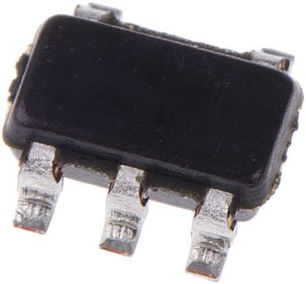
TCM828/TCM829 Switched Capacitor Voltage Converters Features Description • Charge Pump in 5-Pin SOT-23 Package The TCM828/TCM829 devices are CMOS “charge- • >95% Voltage Conversion Efficiency pump” voltage converters in ultra-small, 5-Pin SOT-23 packages. They invert and/or double an input voltage • Voltage Inversion and/or Doubling which can range from +1.5V to +5.5V. Conversion • Low 50µA (TCM828) Quiescent Current efficiency is typically >95%. Switching frequency is • Operates from +1.5V to +5.5V 12kHz for the TCM828, and 35kHz for the TCM829. • Up to 25mA Output Current External component requirement is only two capacitors • Only Two External Capacitors Required (3.3µF nominal) for standard voltage inverter applications. With a few additional components, a Applications positive doubler can also be built. All other circuitry, including control, oscillator and power MOSFETs, are • LCD Panel Bias integrated on-chip. Supply current is 50µA (TCM828) • Cellular Phones and 115µA (TCM829). • Pagers The TCM828 and TCM829 devices are available in a • PDAs, Portable Dataloggers 5-Pin SOT-23 surface mount package. • Battery-Powered Devices Package Type Typical Application Circuit TCM828/TCM829 Voltage Inverter SOT-23 C+ VIN INPUT C1 9 OUT 1 5 C+ 2 8 C- M C T 8/ VIN 2 2 8 M C OUT V- T GND OUTPUT C- 3 4 GND C 2 Ordering Information Temperature Part No. Package Range TCM828ECT 5-Pin SOT-23 -40°C to +85°C TCM828VT 5-Pin SOT-23 -40°C to +125°C TCM829ECT 5-Pin SOT-23 -40°C to +85°C Note: 5-Pin SOT-23 is equivalent to EIAJ SC-74A. © 2010 Microchip Technology Inc. DS21488B-page 1
TCM828/TCM829 NOTES: DS21488B-page 2 © 2010 Microchip Technology Inc.
TCM828/TCM829 1.0 ELECTRICAL † Notice: Stresses above those listed under “Maximum CHARACTERISTICS Ratings” may cause permanent damage to the device. This is a stress rating only and functional operation of the device at those or any other conditions above those Absolute Maximum Ratings † indicated in the operational listings of this specification is not implied. Exposure to maximum rating conditions Input Voltage (V to GND)..................................+30V IN for extended periods may affect device reliability. Output Voltage (OUT to GND)...................6.0V, +0.3V Current at OUT Pin............................................50mA Short-Circuit Duration–OUT to GND............Indefinite Operating Temperature Range................-40°C to +85°C Variable Temp. Range (TCM828 only)............................... .............................................................................-40°C to +125°C Power Dissipation (T ≤70°C)........................240mW A Storage Temperature (Unbiased)..........-65°C to +150°C Lead Temperature (Soldering, 10sec)............ +300°C ELECTRICAL CHARACTERISTICS (0°C TO +85°C) Electrical Specifications: T = 0°C to +85°C, V = +5V, C1 = C2 = 10µF (TCM828), C1 = C2 = 3.3µF (TCM829), A IN unless otherwise noted. Typical values are at T = +25°C. A Parameters Sym Min Typ Max Units Conditions Supply Current I — 50 90 µA TCM828, T = +25°C DD A — 115 260 µA TCM829, T = +25°C A Minimum Supply V+ 1.5 — — V R = 10kΩ, LOAD Voltage T = 0°C to +85°C A Maximum Supply V+ — — 5.5 V R = 10kΩ LOAD Voltage Oscillator Frequency F 8.4 12 15.6 kHz TCM828, T = +25°C OSC A 24.5 35 45.5 kHz TCM829, T = +25°C A Power Efficiency P — 96 — % I = 3mA,T = +25°C EFF LOAD A Voltage Conversion V 95 99.9 — % R = ∞ EFF LOAD Efficiency Output Resistance R — 25 50 Ω I = 5mA,T = +25°C OUT OUT A — — 65 Ω I = 5mA,T = 0°C to +85°C OUT A Note 1: Capacitor contribution is approximately 20% of the output impedance [ESR = 1/pump frequency x capacitance)]. ELECTRICAL CHARACTERISTICS (-40°C TO +85°C) Electrical Specifications: T = -40°C to +85°C, V = +5V, C1 = C2 = 10µF (TCM828), C1 = C2 = 3.3µF A IN (TCM829), unless otherwise noted. Typical values are at T = +25°C. (Note1) A Parameters Sym Min Typ Max Units Conditions Supply Current I — — 115 µA TCM828 DD — — 325 µA TCM829 Supply Voltage Range V+ 1.5 — 5.5 V R = 10kΩ LOAD Oscillator Frequency F 6 — 15.6 kHz TCM828 OSC 19 — 45.5 kHz TCM829 Output Resistance R — — 65 Ω I = 5mA OUT OUT Note 1: All -40°C to +85°C specifications above are assured by design. © 2010 Microchip Technology Inc. DS21488B-page 3
TCM828/TCM829 NOTES: DS21488B-page 4 © 2010 Microchip Technology Inc.
TCM828/TCM829 2.0 TYPICAL CHARACTERISTICS Note: The graphs and tables provided following this note are a statistical summary based on a limited number of samples and are provided for informational purposes only. The performance characteristics listed herein are not tested or guaranteed. In some graphs or tables, the data presented may be outside the specified- operating range (e.g., outside specified power supply range) and therefore outside the warranted range. Note: Circuit of Figure5-3, V = +5V, C1 = C2 = C3, T = +25°C, unless otherwise noted. IN A 70 40 V = 4.75V, V = – 4.0V IN OUT 60 35 Ω) A) ANCE ( 50 ENT (m2350 VIN= 3.15V, VOUT = – 2.5V SIST 40 URR20 T RE 30 TCM828 TCM829 UT C15 TPU 20 UTP10 VIN= 1.9V, VOUT = –1.5V U O O 10 5 0 0 1.5 2.5 3.5 4.5 0 10 20 30 40 SUPPLY VOLTAGE (V) CAPACITANCE (µF) FIGURE 2-1: Output Resistance vs. FIGURE 2-3: TCM828 – Output Current Supply Voltage. vs. Capacitance. 80 40 V = 4.75V, V– = – 4.0V IN 70 35 Ω) V = 1.5V A) ANCE (5600 IN ENT (m3205 VIN= 3.15V, V– = – 2.5V T R SIS 40 UR 20 E C T R 30 VIN= 3.3V UT 15 UTPU 20 VIN= 5.0V OUTP10 VIN= 1.9V, VOUT=– 1.5V O 10 5 0 0 –40°C 0°C 25°C 85°C 0 5 10 15 20 25 30 35 TEMPERATURE (°C) CAPACITANCE(µF) FIGURE 2-2: Output Resistance vs. FIGURE 2-4: TCM829 – Output Current Temperature. vs. Capacitance. © 2010 Microchip Technology Inc. DS21488B-page 5
TCM828/TCM829 Note:Circuit of Figure5-3, V = +5V, C1 = C2 = C3, T = +25°C, unless otherwise noted. IN A 450 14 p-p)400 VIN= 5.0V mV350 VIN= 4.75V, VOUT = – 4.0V Hz) 12 PLE (300 CY (k 10 VIN= 3.3V E RIP250 VIN= 3.15V, VOUT = – 2.5V QUEN 8 VIN= 1.5V AG200 VIN= 1.9V, VOUT = – 1.5V RE 6 OLT150 P F V M 4 UT 100 PU P 2 T 50 U O 0 0 0 5 10 25 20 25 30 35 5 –40 0°C 25°C 85°C CAPACITANCE (µF) TEMPERATURE (°C) FIGURE 2-5: TCM828 – Output Voltage FIGURE 2-8: TCM828 – Pump Frequency Ripple vs. Capacitance. vs. Temperature. 300 45 p) Vp-250 VIN= 4.75V, VOUT = – 4.0V 40 VIN= 5.0V m z) 35 PPLE (200 VIN= 3.15V, VOUT = – 2.5V CY (kH 30 VIN= 3.3V E RI150 UEN 25 VIN= 1.5V G Q 20 A E LT100 VIN= 1.9V, VOUT = – 1.5V FR 15 PUT VO 50 PUMP 10 T 5 U O 0 0 0 5 10 15 20 30 35 –40°C 0°C 25°C 85°C CAPACITANCE (µF) TEMPERATURE (°C) FIGURE 2-6: TCM829 – Output Voltage FIGURE 2-9: TCM829 – Pump Frequency Ripple vs. Capacitance. vs. Temperature. p 120 0 A)100 V) –1 T (µ E ( VIN= 2.0V N 80 G –2 E A URR 60 TCM829 OLT –3 VIN= 3.3V C V Y T PL 40 PU –4 P TCM828 T U U V = 5.0V S O IN 20 –5 0 –6 1.5 2 2.5 3 3.5 4 4.5 5 5.5 0 10 20 30 40 50 SUPPLY VOLTAGE (V) OUTPUT CURRENT (mA) FIGURE 2-7: Supply Current vs. Supply FIGURE 2-10: Output Voltage vs. Output Voltage. Current. DS21488B-page 6 © 2010 Microchip Technology Inc.
TCM828/TCM829 Note: Circuit of Figure5-3, V = +5V, C1 = C2 = C3, T = +25°C, unless otherwise noted. IN A y p 100 V = 5.0V IN %) 80 CY ( VIN= 3.3V N E VIN=1.5V CI FI F 60 E 40 0 10 20 30 40 50 OUTPUT CURRENT (mA) FIGURE 2-11: Efficiency vs. Output Current. © 2010 Microchip Technology Inc. DS21488B-page 7
TCM828/TCM829 NOTES: DS21488B-page 8 © 2010 Microchip Technology Inc.
TCM828/TCM829 3.0 PIN DESCRIPTION The descriptions of the pins are listed in Table3-1. TABLE 3-1: PIN FUNCTION TABLE TCM828/TCM829 Symbol Function SOT-23 1 OUT Inverting charge pump output 2 V Positive power supply input IN 3 C - Commutation capacitor negative terminal 1 4 GND Ground 5 C + Commutation capacitor positive terminal 1 © 2010 Microchip Technology Inc. DS21488B-page 9
TCM828/TCM829 NOTES: DS21488B-page 10 © 2010 Microchip Technology Inc.
TCM828/TCM829 4.0 DETAILED DESCRIPTION The TCM828/TCM829 charge pump converters invert the voltage applied to the V pin. Conversion consists IN of a two phase operation (Figure4-1). During the first phase, switches S2 and S4 are open, while S1 and S3 are closed. During this time, C1 charges to the voltage on V and load current is supplied from C2. During the IN second phase, S2 and S4 are closed, and S1 and S3 are open. This action connects C1 across C2, restoring charge to C2. S1 S2 IN TCM828/ TCM829 C1 C2 S3 S4 V =-(V ) OUT IN FIGURE 4-1: Ideal Switched Capacitor Charge Pump. © 2010 Microchip Technology Inc. DS21488B-page 11
TCM828/TCM829 NOTES: DS21488B-page 12 © 2010 Microchip Technology Inc.
TCM828/TCM829 5.0 APPLICATIONS INFORMATION The losses in the circuit due to factor 4 above are also shown in Equation5-2. The output voltage ripple is 5.0.1 OUTPUT VOLTAGE shown in Equation5-3. CONSIDERATIONS EQUATION 5-2: The TCM828/TCM829 devices perform voltage conversion, but do not provide regulation. The output P = [(0.5)(C1)(V 2+V 2)+(0.5)(C2)(V 2– LOSS(4) IN OUT RIPPLE voltage will droop in a linear manner with respect to –2V V ]×f load current. The value of this equivalent output OUT RIPPLE OSC resistance is approximately 25Ω nominal at +25°C and VIN = +5V. VOUT is approximately – 5V at light loads, EQUATION 5-3: and droops according to the equation below: VDROOP=IOUT×ROUT V = ---------I--O----U---T----------+2(I )(ESR ) RIPPLE (f )(C2) OUT C2 V =–(V –V ) OSC OUT IN DROOP 5.0.2 CHARGE PUMP EFFICIENCY The overall power efficiency of the charge pump is f affected by four factors: V+ V OUT 1. Losses from power consumed by the internal oscillator, switch drive, etc. (which vary with input voltage, temperature and oscillator C1 C2 RL frequency). 2. I2R losses due to the on-resistance of the MOSFET switches on-board the charge pump. 3. Charge pump capacitor losses due to effective FIGURE 5-1: Ideal Switched Capacitor series resistance (ESR). Model. 4. Losses that occur during charge transfer (from the commutation capacitor to the output capacitor) when a voltage difference between REQUIV the two capacitors exists. V+ VOUT Most of the conversion losses are due to factors 2, 3 1 and 4 above. These losses are shown in Equation5-1. REQUIV= f---×------C----1-- C2 RL EQUATION 5-1: P = I 2×R LOSS(2,3,4) OUT OUT FIGURE 5-2: Equivalent Output ≅I 2× ------------1--------------+8R +4ESR +ESR Resistance. OUT (f )C1 SWITCH C1 C2 OSC The 1/(f )(C1) term in Equation5-1 is the effective OSC output resistance of an ideal switched capacitor circuit (Figures5-1 and 5-2). © 2010 Microchip Technology Inc. DS21488B-page 13
TCM828/TCM829 5.0.3 CAPACITOR SELECTION 5.0.5 VOLTAGE INVERTER In order to maintain the lowest output resistance and The most common application for charge pump output ripple voltage, it is recommended that low ESR devices is the inverter (Figure5-3). This application capacitors be used. Additionally, larger values of C1 will uses two external capacitors – C1 and C2 (plus a lower the output resistance and larger values of C2 will power supply bypass capacitor, if necessary). The reduce output ripple. (See Equation5-1). output is equal to V– plus any voltage drops, due to IN loading. Refer to Table5-1 and Table5-1 for capacitor Table5-1 shows various values of C1 and the selection. corresponding output resistance values @ +25°C. It assumes a 0.1ΩESR and 2ΩR . Table5-2 shows C1 SW the output voltage ripple for various values of C2. The V OUT VRIPPLE values assume 10mA output load current and C3 0.1ΩESR . 3.3µF* C2 TABLE 5-1: OUTPUT RESISTANCE VS. C1 VOUT (ESR = 0.1Ω) 1 OUT C1+5 C2 C1 (µF) TCM828 ROUT (Ω) TCM829 ROUT (Ω) 8/9 3.3µF* 22 C1 0.1 850 302 2 IN M8M8 3.3µF* RL 1 100 45 CC 3.3 42 25 3 C1-TTGND 4 10 25 19 47 18 17 Voltage Inverter 100 17 17 *10µF (TCM828) I TABLE 5-2: OUTPUT VOLTAGE RIPPLE FIGURE 5-3: Test Circuit. VS. C2 (ESR = 0.1Ω) IOUT 10MA 5.0.6 CASCADING DEVICES TCM828 V Two or more TCM828/829 devices can be cascaded to C2 (µF) RIPPLE TCM829 R (Ω) (mV) OUT increase output voltage (Table5-4). If the output is lightly loaded, it will be close to (– 2 x VIN) but will droop 1 835 286 at least by R of the first device multiplied by the IQ OUT 3.3 254 88 of the second. It can be seen that the output resistance 10 85 31 rises rapidly for multiple cascaded devices. For large negative voltage requirements see the TC682 or 47 20 8 TCM680 data sheets. 100 10 5 5.0.4 INPUT SUPPLY BYPASSING . . . V+ The V input should be capacitively bypassed to IN IN reduce AC impedance and minimize noise effects due 2 2 to the switching internal to the device. The 3 TCM828/ 3 TCM828/ recommended capacitor depends on the configuration C1 4 TCM829 4 TCM829 C1 of the TCM828/TCM829 devices. 5 "1" 1 5 "n" 1 VOUT If the device is loaded from OUT to GND, it is . . . recommended that a large value capacitor (at least C2 C2 equal to C1) be connected from the input to GND. If the device is loaded from IN to OUT, a small (0.1µF) V =-nV OUT IN capacitor is sufficient. FIGURE 5-4: Cascading TCM828 or TCM829 Devices to Increase Output Voltage. DS21488B-page 14 © 2010 Microchip Technology Inc.
TCM828/TCM829 5.0.7 PARALLELING DEVICES To reduce the value of R , multiple TCM828/ V+IN OUT TCM829 devices can be connected in parallel D1, D2 = 1N4148 (Figure5-5). The output resistance will be reduced by 3 2 a factor of N, where N is the number of TCM828/ C1 TCM828/ TCM829 device. Each device will require it’s own pump 4 TCM829 D1 capacitor (C1), but all devices may share one reservoir capacitor (C2). However, to preserve ripple performance, the value of C2 should be scaled 5 1 VOUT=V-IN according to the number of paralleled TCM828/ C2 TCM829 devices. D2 VOUT=(2VIN)- C3 (VFD1)-(VFD2) V OF SINGLE DEVICE R = OUT C4 OUT NUMBEROFDEVICES V+ . . . IN FIGURE 5-6: Combined Doubler and 2 2 Inverter. 3 3 TCM828/ TCM828/ 5.0.9 DIODE PROTECTION FOR HEAVY C1 4 TCM829 4 TCM829 C1 LOADS 5 "1" 1 5 "n" 1 VOUT When heavy loads require the OUT pin to sink large currents, being delivered by a positive source, diode . . . V =V- C2 protection may be needed. The OUT pin should not be OUT IN allowed to be pulled above ground. This is accomplished by connecting a Schottky diode FIGURE 5-5: Paralleling TCM828 or (1N5817) as shown in Figure5-7. TCM829 Devices to Reduce Output Resistance. 4 5.0.8 VOLTAGE DOUBLER/INVERTER GND Another common application of the TCM828/TCM829 devices is shown in Figure5-6. This circuit performs TCM828/ two functions in combination. C1 and C2 form the TCM829 standard inverter circuit described above. C3 and C4, plus the two diodes, form the voltage doubler circuit. C1 and C3 are the pump capacitors, while C2 and C4 are 1 OUT the reservoir capacitors. Because both sub-circuits rely on the same switches, if either output is loaded, both FIGURE 5-7: High V– Load Current. will drop toward GND. Make sure that the total current drawn from both the outputs does not total more than 5.0.10 LAYOUT CONSIDERATIONS 40mA. As with any switching power supply circuit, good layout practice is recommended. Mount components as close together as possible, to minimize stray inductance and capacitance. Also use a large ground plane to minimize noise leakage into other circuitry. © 2010 Microchip Technology Inc. DS21488B-page 15
TCM828/TCM829 NOTES: DS21488B-page 16 © 2010 Microchip Technology Inc.
TCM828/TCM829 6.0 PACKAGING INFORMATION 6.1 Package Marking Information 5-Lead SOT-23 Example: Device Code TCM828ECT728 CANN XXNN CA25 TCM828VT713 CWNN TCM829ECT713-GVAO CBNN Legend: XX...X Customer-specific information Y Year code (last digit of calendar year) YY Year code (last 2 digits of calendar year) WW Week code (week of January 1 is week ‘01’) NNN Alphanumeric traceability code e3 Pb-free JEDEC designator for Matte Tin (Sn) * This package is Pb-free. The Pb-free JEDEC designator ( e 3 ) can be found on the outer packaging for this package. Note: In the event the full Microchip part number cannot be marked on one line, it will be carried over to the next line, thus limiting the number of available characters for customer-specific information. © 2010 Microchip Technology Inc. DS21488B-page 17
TCM828/TCM829 PIN 1 User Direction of Feed User Direction of Feed Device gnikraM Marking eciveD W PIN 1 P Standard Reel Component Orientation Reverse Reel Component Orientation TR Suffix Device RT Suffix Device (Mark Right Side Up) (Mark Upside Down) Carrier Tape, Number of Components Per Reel and Reel Size Package Carrier Width (W) Pitch (P) Part Per Full Reel Reel Size 5-Pin SOT-23 8 mm 4 mm 3000 7 in FIGURE 6-1: Component Taping Orientation for 5-Pin SOT-23 (EIAJ SC-74A) Devices. DS21488B-page 18 © 2010 Microchip Technology Inc.
TCM828/TCM829 (cid:2)(cid:3)(cid:4)(cid:5)(cid:6)(cid:7)(cid:8)(cid:9)(cid:10)(cid:6)(cid:11)(cid:12)(cid:13)(cid:14)(cid:8)(cid:15)(cid:16)(cid:6)(cid:10)(cid:10)(cid:8)(cid:17)(cid:18)(cid:12)(cid:10)(cid:13)(cid:19)(cid:5)(cid:8)(cid:20)(cid:21)(cid:6)(cid:19)(cid:11)(cid:13)(cid:11)(cid:12)(cid:22)(cid:21)(cid:8)(cid:23)(cid:24)(cid:20)(cid:25)(cid:8)(cid:26)(cid:15)(cid:17)(cid:20)(cid:3)(cid:27)(cid:28)(cid:29) (cid:30)(cid:22)(cid:12)(cid:5)(cid:31) .(cid:10)(cid:9)(cid:2)$(cid:11)(cid:14)(cid:2) (cid:10)!$(cid:2)(cid:8)%(cid:9)(cid:9)(cid:14)(cid:15)$(cid:2)(cid:12)(cid:28)(cid:8)/(cid:28)(cid:17)(cid:14)(cid:2)"(cid:9)(cid:28)-(cid:7)(cid:15)(cid:17)!0(cid:2)(cid:12)(cid:16)(cid:14)(cid:28)!(cid:14)(cid:2)!(cid:14)(cid:14)(cid:2)$(cid:11)(cid:14)(cid:2)(cid:6)(cid:7)(cid:8)(cid:9)(cid:10)(cid:8)(cid:11)(cid:7)(cid:12)(cid:2)1(cid:28)(cid:8)/(cid:28)(cid:17)(cid:7)(cid:15)(cid:17)(cid:2)(cid:22)(cid:12)(cid:14)(cid:8)(cid:7)&(cid:7)(cid:8)(cid:28)$(cid:7)(cid:10)(cid:15)(cid:2)(cid:16)(cid:10)(cid:8)(cid:28)$(cid:14)"(cid:2)(cid:28)$(cid:2) (cid:11)$$(cid:12)+22---(cid:20) (cid:7)(cid:8)(cid:9)(cid:10)(cid:8)(cid:11)(cid:7)(cid:12)(cid:20)(cid:8)(cid:10) 2(cid:12)(cid:28)(cid:8)/(cid:28)(cid:17)(cid:7)(cid:15)(cid:17) b N E E1 1 2 3 e e1 D A A2 c φ A1 L L1 3(cid:15)(cid:7)$! (cid:6)(cid:19)44(cid:19)(cid:6)#(cid:13)#(cid:26)(cid:22) (cid:21)(cid:7) (cid:14)(cid:15)!(cid:7)(cid:10)(cid:15)(cid:2)4(cid:7) (cid:7)$! (cid:6)(cid:19)5 56(cid:6) (cid:6)(cid:25)7 5% 8(cid:14)(cid:9)(cid:2)(cid:10)&(cid:2)1(cid:7)(cid:15)! 5 (cid:30) 4(cid:14)(cid:28)"(cid:2)1(cid:7)$(cid:8)(cid:11) (cid:14) (cid:4)(cid:20)(cid:24)(cid:30)(cid:2))(cid:22)* 6%$!(cid:7)"(cid:14)(cid:2)4(cid:14)(cid:28)"(cid:2)1(cid:7)$(cid:8)(cid:11) (cid:14)(cid:31) (cid:31)(cid:20)(cid:24)(cid:4)(cid:2))(cid:22)* 6,(cid:14)(cid:9)(cid:28)(cid:16)(cid:16)(cid:2)9(cid:14)(cid:7)(cid:17)(cid:11)$ (cid:25) (cid:4)(cid:20)(cid:24)(cid:4) : (cid:31)(cid:20)(cid:23)(cid:30) (cid:6)(cid:10)(cid:16)"(cid:14)"(cid:2)1(cid:28)(cid:8)/(cid:28)(cid:17)(cid:14)(cid:2)(cid:13)(cid:11)(cid:7)(cid:8)/(cid:15)(cid:14)!! (cid:25)(cid:3) (cid:4)(cid:20);(cid:24) : (cid:31)(cid:20)(cid:29)(cid:4) (cid:22)$(cid:28)(cid:15)"(cid:10)&& (cid:25)(cid:31) (cid:4)(cid:20)(cid:4)(cid:4) : (cid:4)(cid:20)(cid:31)(cid:30) 6,(cid:14)(cid:9)(cid:28)(cid:16)(cid:16)(cid:2)<(cid:7)"$(cid:11) # (cid:3)(cid:20)(cid:3)(cid:4) : (cid:29)(cid:20)(cid:3)(cid:4) (cid:6)(cid:10)(cid:16)"(cid:14)"(cid:2)1(cid:28)(cid:8)/(cid:28)(cid:17)(cid:14)(cid:2)<(cid:7)"$(cid:11) #(cid:31) (cid:31)(cid:20)(cid:29)(cid:4) : (cid:31)(cid:20);(cid:4) 6,(cid:14)(cid:9)(cid:28)(cid:16)(cid:16)(cid:2)4(cid:14)(cid:15)(cid:17)$(cid:11) (cid:21) (cid:3)(cid:20)(cid:5)(cid:4) : (cid:29)(cid:20)(cid:31)(cid:4) .(cid:10)(cid:10)$(cid:2)4(cid:14)(cid:15)(cid:17)$(cid:11) 4 (cid:4)(cid:20)(cid:31)(cid:4) : (cid:4)(cid:20)=(cid:4) .(cid:10)(cid:10)$(cid:12)(cid:9)(cid:7)(cid:15)$ 4(cid:31) (cid:4)(cid:20)(cid:29)(cid:30) : (cid:4)(cid:20);(cid:4) .(cid:10)(cid:10)$(cid:2)(cid:25)(cid:15)(cid:17)(cid:16)(cid:14) (cid:3) (cid:4)> : (cid:29)(cid:4)> 4(cid:14)(cid:28)"(cid:2)(cid:13)(cid:11)(cid:7)(cid:8)/(cid:15)(cid:14)!! (cid:8) (cid:4)(cid:20)(cid:4); : (cid:4)(cid:20)(cid:3)= 4(cid:14)(cid:28)"(cid:2)<(cid:7)"$(cid:11) 8 (cid:4)(cid:20)(cid:3)(cid:4) : (cid:4)(cid:20)(cid:30)(cid:31) (cid:30)(cid:22)(cid:12)(cid:5)(cid:11)(cid:31) (cid:31)(cid:20) (cid:21)(cid:7) (cid:14)(cid:15)!(cid:7)(cid:10)(cid:15)!(cid:2)(cid:21)(cid:2)(cid:28)(cid:15)"(cid:2)#(cid:31)(cid:2)"(cid:10)(cid:2)(cid:15)(cid:10)$(cid:2)(cid:7)(cid:15)(cid:8)(cid:16)%"(cid:14)(cid:2) (cid:10)(cid:16)"(cid:2)&(cid:16)(cid:28)!(cid:11)(cid:2)(cid:10)(cid:9)(cid:2)(cid:12)(cid:9)(cid:10)$(cid:9)%!(cid:7)(cid:10)(cid:15)!(cid:20)(cid:2)(cid:6)(cid:10)(cid:16)"(cid:2)&(cid:16)(cid:28)!(cid:11)(cid:2)(cid:10)(cid:9)(cid:2)(cid:12)(cid:9)(cid:10)$(cid:9)%!(cid:7)(cid:10)(cid:15)!(cid:2)!(cid:11)(cid:28)(cid:16)(cid:16)(cid:2)(cid:15)(cid:10)$(cid:2)(cid:14)’(cid:8)(cid:14)(cid:14)"(cid:2)(cid:4)(cid:20)(cid:31)(cid:3)(cid:5)(cid:2) (cid:2)(cid:12)(cid:14)(cid:9)(cid:2)!(cid:7)"(cid:14)(cid:20) (cid:3)(cid:20) (cid:21)(cid:7) (cid:14)(cid:15)!(cid:7)(cid:10)(cid:15)(cid:7)(cid:15)(cid:17)(cid:2)(cid:28)(cid:15)"(cid:2)$(cid:10)(cid:16)(cid:14)(cid:9)(cid:28)(cid:15)(cid:8)(cid:7)(cid:15)(cid:17)(cid:2)(cid:12)(cid:14)(cid:9)(cid:2)(cid:25)(cid:22)(cid:6)#(cid:2)((cid:31)(cid:23)(cid:20)(cid:30)(cid:6)(cid:20) )(cid:22)*+ )(cid:28)!(cid:7)(cid:8)(cid:2)(cid:21)(cid:7) (cid:14)(cid:15)!(cid:7)(cid:10)(cid:15)(cid:20)(cid:2)(cid:13)(cid:11)(cid:14)(cid:10)(cid:9)(cid:14)$(cid:7)(cid:8)(cid:28)(cid:16)(cid:16)(cid:18)(cid:2)(cid:14)’(cid:28)(cid:8)$(cid:2),(cid:28)(cid:16)%(cid:14)(cid:2)!(cid:11)(cid:10)-(cid:15)(cid:2)-(cid:7)$(cid:11)(cid:10)%$(cid:2)$(cid:10)(cid:16)(cid:14)(cid:9)(cid:28)(cid:15)(cid:8)(cid:14)!(cid:20) (cid:6)(cid:7)(cid:8)(cid:9)(cid:10)(cid:8)(cid:11)(cid:7)(cid:12)(cid:13)(cid:14)(cid:8)(cid:11)(cid:15)(cid:10)(cid:16)(cid:10)(cid:17)(cid:18)(cid:21)(cid:9)(cid:28)-(cid:7)(cid:15)(cid:17)*(cid:4)(cid:23)(cid:27)(cid:4)(cid:24)(cid:31)) © 2010 Microchip Technology Inc. DS21488B-page 19
TCM828/TCM829 5-Lead Plastic Small Outline Transistor (CT) [SOT-23] Note: For the most current package drawings, please see the Microchip Packaging Specification located at http://www.microchip.com/packaging DS21488B-page 20 © 2010 Microchip Technology Inc.
TCM828/TCM829 APPENDIX A: REVISION HISTORY Revision B (August 2010) The following is the list of modifications: 1. Added new operating temperature for TCM828 (TCM828VT). 2. Reformatted the original document. 3. Updated package drawings. Revision A (March 2001) • Original Release of this Document. © 2010 Microchip Technology Inc. DS21488B-page 21
TCM828/TCM829 NOTES: DS21488B-page 22 © 2010 Microchip Technology Inc.
TCM828/TCM829 PRODUCT IDENTIFICATION SYSTEM To order or obtain information, e.g., on pricing or delivery, refer to the factory or the listed sales office. PART NO. X /XX Examples: Device Temperature Package a) TCM828ECT728: Extended Temp., Range 5-LD SOT-23 Package. b) TCM828VT713: Various Temperature Device: TCM828: CMOS Voltage Converter. TCM829: CMOS Voltage Converter. 5-LD SOT-23 Package. c) TCM829ECT713-GVAO: Temperature Range: E = -40°C to +85°C V = -40°C to +125°C Extended Temp., 5-LD SOT-23 Package. Package: CT = 5-Lead Plastic Small Outline Transistor, SOT-23. © 2010 Microchip Technology Inc. DS21488B-page 23
TCM828/TCM829 NOTES: DS21488B-page 24 © 2010 Microchip Technology Inc.
Note the following details of the code protection feature on Microchip devices: • Microchip products meet the specification contained in their particular Microchip Data Sheet. • Microchip believes that its family of products is one of the most secure families of its kind on the market today, when used in the intended manner and under normal conditions. • There are dishonest and possibly illegal methods used to breach the code protection feature. All of these methods, to our knowledge, require using the Microchip products in a manner outside the operating specifications contained in Microchip’s Data Sheets. Most likely, the person doing so is engaged in theft of intellectual property. • Microchip is willing to work with the customer who is concerned about the integrity of their code. • Neither Microchip nor any other semiconductor manufacturer can guarantee the security of their code. Code protection does not mean that we are guaranteeing the product as “unbreakable.” Code protection is constantly evolving. We at Microchip are committed to continuously improving the code protection features of our products. Attempts to break Microchip’s code protection feature may be a violation of the Digital Millennium Copyright Act. If such acts allow unauthorized access to your software or other copyrighted work, you may have a right to sue for relief under that Act. Information contained in this publication regarding device Trademarks applications and the like is provided only for your convenience The Microchip name and logo, the Microchip logo, dsPIC, and may be superseded by updates. It is your responsibility to KEELOQ, KEELOQ logo, MPLAB, PIC, PICmicro, PICSTART, ensure that your application meets with your specifications. PIC32 logo, rfPIC and UNI/O are registered trademarks of MICROCHIP MAKES NO REPRESENTATIONS OR Microchip Technology Incorporated in the U.S.A. and other WARRANTIES OF ANY KIND WHETHER EXPRESS OR countries. IMPLIED, WRITTEN OR ORAL, STATUTORY OR OTHERWISE, RELATED TO THE INFORMATION, FilterLab, Hampshire, HI-TECH C, Linear Active Thermistor, INCLUDING BUT NOT LIMITED TO ITS CONDITION, MXDEV, MXLAB, SEEVAL and The Embedded Control QUALITY, PERFORMANCE, MERCHANTABILITY OR Solutions Company are registered trademarks of Microchip FITNESS FOR PURPOSE. Microchip disclaims all liability Technology Incorporated in the U.S.A. arising from this information and its use. Use of Microchip Analog-for-the-Digital Age, Application Maestro, CodeGuard, devices in life support and/or safety applications is entirely at dsPICDEM, dsPICDEM.net, dsPICworks, dsSPEAK, ECAN, the buyer’s risk, and the buyer agrees to defend, indemnify and ECONOMONITOR, FanSense, HI-TIDE, In-Circuit Serial hold harmless Microchip from any and all damages, claims, Programming, ICSP, Mindi, MiWi, MPASM, MPLAB Certified suits, or expenses resulting from such use. No licenses are logo, MPLIB, MPLINK, mTouch, Octopus, Omniscient Code conveyed, implicitly or otherwise, under any Microchip Generation, PICC, PICC-18, PICDEM, PICDEM.net, PICkit, intellectual property rights. PICtail, REAL ICE, rfLAB, Select Mode, Total Endurance, TSHARC, UniWinDriver, WiperLock and ZENA are trademarks of Microchip Technology Incorporated in the U.S.A. and other countries. SQTP is a service mark of Microchip Technology Incorporated in the U.S.A. All other trademarks mentioned herein are property of their respective companies. © 2010, Microchip Technology Incorporated, Printed in the U.S.A., All Rights Reserved. Printed on recycled paper. ISBN: 978-1-60932-445-2 Microchip received ISO/TS-16949:2002 certification for its worldwide headquarters, design and wafer fabrication facilities in Chandler and Tempe, Arizona; Gresham, Oregon and design centers in California and India. The Company’s quality system processes and procedures are for its PIC® MCUs and dsPIC® DSCs, KEELOQ® code hopping devices, Serial EEPROMs, microperipherals, nonvolatile memory and analog products. In addition, Microchip’s quality system for the design and manufacture of development systems is ISO 9001:2000 certified. © 2010 Microchip Technology Inc. DS21488B-page 25
WORLDWIDE SALES AND SERVICE AMERICAS ASIA/PACIFIC ASIA/PACIFIC EUROPE Corporate Office Asia Pacific Office India - Bangalore Austria - Wels 2355 West Chandler Blvd. Suites 3707-14, 37th Floor Tel: 91-80-3090-4444 Tel: 43-7242-2244-39 Chandler, AZ 85224-6199 Tower 6, The Gateway Fax: 91-80-3090-4123 Fax: 43-7242-2244-393 Tel: 480-792-7200 Harbour City, Kowloon India - New Delhi Denmark - Copenhagen Fax: 480-792-7277 Hong Kong Tel: 91-11-4160-8631 Tel: 45-4450-2828 Technical Support: Tel: 852-2401-1200 Fax: 91-11-4160-8632 Fax: 45-4485-2829 http://support.microchip.com Web Address: Fax: 852-2401-3431 India - Pune France - Paris www.microchip.com Australia - Sydney Tel: 91-20-2566-1512 Tel: 33-1-69-53-63-20 Tel: 61-2-9868-6733 Fax: 91-20-2566-1513 Fax: 33-1-69-30-90-79 ADtullaunthta, GA Fax: 61-2-9868-6755 Japan - Yokohama Germany - Munich Tel: 678-957-9614 China - Beijing Tel: 81-45-471- 6166 Tel: 49-89-627-144-0 Tel: 86-10-8528-2100 Fax: 49-89-627-144-44 Fax: 678-957-1455 Fax: 81-45-471-6122 Fax: 86-10-8528-2104 Italy - Milan Boston Korea - Daegu Westborough, MA China - Chengdu Tel: 82-53-744-4301 Tel: 39-0331-742611 Tel: 774-760-0087 Tel: 86-28-8665-5511 Fax: 82-53-744-4302 Fax: 39-0331-466781 Fax: 774-760-0088 Fax: 86-28-8665-7889 Korea - Seoul Netherlands - Drunen Chicago China - Chongqing Tel: 82-2-554-7200 Tel: 31-416-690399 Itasca, IL Tel: 86-23-8980-9588 Fax: 82-2-558-5932 or Fax: 31-416-690340 Tel: 630-285-0071 Fax: 86-23-8980-9500 82-2-558-5934 Spain - Madrid Fax: 630-285-0075 China - Hong Kong SAR Malaysia - Kuala Lumpur Tel: 34-91-708-08-90 Cleveland Tel: 852-2401-1200 Tel: 60-3-6201-9857 Fax: 34-91-708-08-91 Independence, OH Fax: 852-2401-3431 Fax: 60-3-6201-9859 UK - Wokingham Tel: 216-447-0464 China - Nanjing Malaysia - Penang Tel: 44-118-921-5869 Fax: 216-447-0643 Tel: 86-25-8473-2460 Tel: 60-4-227-8870 Fax: 44-118-921-5820 Dallas Fax: 86-25-8473-2470 Fax: 60-4-227-4068 Addison, TX China - Qingdao Philippines - Manila Tel: 972-818-7423 Tel: 86-532-8502-7355 Tel: 63-2-634-9065 Fax: 972-818-2924 Fax: 86-532-8502-7205 Fax: 63-2-634-9069 Detroit China - Shanghai Singapore Farmington Hills, MI Tel: 86-21-5407-5533 Tel: 65-6334-8870 Tel: 248-538-2250 Fax: 86-21-5407-5066 Fax: 65-6334-8850 Fax: 248-538-2260 China - Shenyang Taiwan - Hsin Chu Kokomo Tel: 86-24-2334-2829 Tel: 886-3-6578-300 Kokomo, IN Fax: 86-24-2334-2393 Fax: 886-3-6578-370 Tel: 765-864-8360 Fax: 765-864-8387 China - Shenzhen Taiwan - Kaohsiung Tel: 86-755-8203-2660 Tel: 886-7-213-7830 Los Angeles Fax: 86-755-8203-1760 Fax: 886-7-330-9305 Mission Viejo, CA Tel: 949-462-9523 China - Wuhan Taiwan - Taipei Tel: 86-27-5980-5300 Tel: 886-2-2500-6610 Fax: 949-462-9608 Fax: 86-27-5980-5118 Fax: 886-2-2508-0102 Santa Clara China - Xian Thailand - Bangkok Santa Clara, CA Tel: 408-961-6444 Tel: 86-29-8833-7252 Tel: 66-2-694-1351 Fax: 408-961-6445 Fax: 86-29-8833-7256 Fax: 66-2-694-1350 China - Xiamen Toronto Mississauga, Ontario, Tel: 86-592-2388138 Canada Fax: 86-592-2388130 Tel: 905-673-0699 China - Zhuhai Fax: 905-673-6509 Tel: 86-756-3210040 Fax: 86-756-3210049 07/15/10 DS21488B-page 26 © 2010 Microchip Technology Inc.