ICGOO在线商城 > 集成电路(IC) > PMIC - 稳压器 - DC DC 开关稳压器 > TC7662ACPA
 Datasheet下载
- 型号: TC7662ACPA
- 制造商: Microchip
- 库位|库存: xxxx|xxxx
- 要求:
| 数量阶梯 | 香港交货 | 国内含税 |
| +xxxx | $xxxx | ¥xxxx |
查看当月历史价格
查看今年历史价格
TC7662ACPA产品简介:
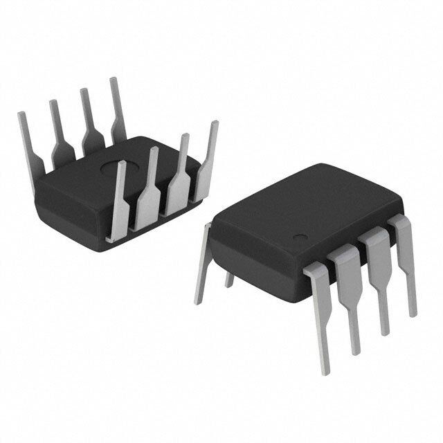
ICGOO电子元器件商城为您提供TC7662ACPA由Microchip设计生产,在icgoo商城现货销售,并且可以通过原厂、代理商等渠道进行代购。 TC7662ACPA价格参考¥25.17-¥39.25。MicrochipTC7662ACPA封装/规格:PMIC - 稳压器 - DC DC 开关稳压器, 固定 充电泵 开关稳压器 IC 正或负 -Vin,2Vin 1 输出 40mA 8-DIP(0.300",7.62mm)。您可以下载TC7662ACPA参考资料、Datasheet数据手册功能说明书,资料中有TC7662ACPA 详细功能的应用电路图电压和使用方法及教程。
Microchip Technology的TC7662ACPA是一款PMIC(电源管理集成电路)中的DC-DC开关稳压器,主要用于高效、紧凑和低功耗的应用场景。以下是其主要应用场景:

1. 便携式电子设备:
   TC7662ACPA适用于电池供电的便携式设备,如智能手机、平板电脑、可穿戴设备(智能手表、健身追踪器)和便携式医疗设备。它能够提供高效的电压转换,延长电池使用寿命。

2. 物联网(IoT)设备:
   在低功耗IoT设备中,例如传感器节点、智能家居设备和无线通信模块,该芯片可以为微控制器、传感器和其他外围设备提供稳定的电源输出。

3. 工业自动化:
   用于工业控制板、数据采集系统和小型嵌入式设备中,为各种负载提供稳定且高效的电源支持,同时满足严格的能效要求。

4. 消费类电子产品:
   包括数码相机、蓝牙耳机、游戏控制器等需要小尺寸和高效率电源解决方案的产品。其紧凑的设计和简单的外部元件配置非常适合这些应用。

5. 医疗设备:
   在便携式医疗设备(如血糖仪、脉搏血氧仪)中,TC7662ACPA能够确保设备在低功耗模式下运行,同时保持性能稳定。

6. 汽车电子:
   虽然TC7662ACPA并非专为汽车设计,但在某些非关键车载应用中(如后视镜摄像头或娱乐系统),它可以作为辅助电源使用。

总结来说,TC7662ACPA凭借其高效率、小尺寸和简单的设计特点,广泛应用于需要低功耗、高效电源管理的各种领域,特别适合对空间和能耗有严格要求的小型化设备。
| 参数 | 数值 |
| 产品目录 | 集成电路 (IC)半导体 |
| 描述 | IC REG SWITCHED CAP INV ADJ 8DIP稳压器—开关式稳压器 High Voltage |
| 产品分类 | |
| 品牌 | Microchip Technology |
| 产品手册 | |
| 产品图片 |
|
| rohs | 符合RoHS无铅 / 符合限制有害物质指令(RoHS)规范要求 |
| 产品系列 | 电源管理 IC,稳压器—开关式稳压器,Microchip Technology TC7662ACPA- |
| 数据手册 | http://www.microchip.com/mymicrochip/filehandler.aspx?ddocname=en026002http://www.microchip.com/mymicrochip/filehandler.aspx?ddocname=en011625http://www.microchip.com/mymicrochip/filehandler.aspx?ddocname=en023833 |
| 产品型号 | TC7662ACPA |
| PCN组件/产地 | http://www.microchip.com/mymicrochip/NotificationDetails.aspx?id=5776&print=view |
| PWM类型 | - |
| 产品目录页面 | |
| 产品种类 | 稳压器—开关式稳压器 |
| 供应商器件封装 | 8-PDIP |
| 其它名称 | 158-1138 |
| 包装 | 管件 |
| 同步整流器 | 无 |
| 商标 | Microchip Technology |
| 安装类型 | 通孔 |
| 安装风格 | Through Hole |
| 宽度 | 6.6 mm |
| 封装 | Tube |
| 封装/外壳 | 8-DIP(0.300",7.62mm) |
| 封装/箱体 | PDIP-8 |
| 工作温度 | 0°C ~ 70°C |
| 工厂包装数量 | 60 |
| 开关频率 | 12 kHz |
| 最大工作温度 | + 70 C |
| 最大输入电压 | 18 V |
| 最小工作温度 | 0 C |
| 标准包装 | 60 |
| 电压-输入 | 3 V ~ 18 V |
| 电压-输出 | -3 V ~ -18 V |
| 电流-输出 | 40mA |
| 类型 | Charge Pump |
| 输出数 | 1 |
| 输出电压 | - 3 V to - 18 V |
| 输出电流 | 40 mA |
| 输出类型 | 可调式 |
| 频率-开关 | 12kHz |


- 商务部:美国ITC正式对集成电路等产品启动337调查
- 曝三星4nm工艺存在良率问题 高通将骁龙8 Gen1或转产台积电
- 太阳诱电将投资9.5亿元在常州建新厂生产MLCC 预计2023年完工
- 英特尔发布欧洲新工厂建设计划 深化IDM 2.0 战略
- 台积电先进制程称霸业界 有大客户加持明年业绩稳了
- 达到5530亿美元!SIA预计今年全球半导体销售额将创下新高
- 英特尔拟将自动驾驶子公司Mobileye上市 估值或超500亿美元
- 三星加码芯片和SET,合并消费电子和移动部门,撤换高东真等 CEO
- 三星电子宣布重大人事变动 还合并消费电子和移动部门
- 海关总署:前11个月进口集成电路产品价值2.52万亿元 增长14.8%


PDF Datasheet 数据手册内容提取
TC7662A Charge Pump DC-to-DC Converter Features Package Type • Wide Operating Range 8-Pin PDIP - 3V to 18V 8-Pin CERDIP • Increased Output Current (40mA) • Pin Compatible with ICL7662/SI7661/TC7660/ NC 1 8 VDD LTC1044 C+ 2 7 OSC TC7662A • No External Diodes Required GND 3 6 NC • Low Output Impedance @ I = 20mA L - 40 Typ. C– 4 5 VOUT • No Low-Voltage Terminal Required • CMOS Construction General Description • Available in 8-Pin PDIP and 8-Pin CERDIP Packages The TC7662A is a pin-compatible upgrade to the industry standard TC7660 charge pump voltage Applications converter. It converts a +3V to +18V input to a corresponding -3V to -18V output using only two low- • Laptop Computers cost capacitors, eliminating inductors and their • Disk Drives associated cost, size and EMI. In addition to a wider • Process Instrumentation power supply input range (3V to 18V versus 1.5V to 10V for the TC7660), the TC7662A can source output • P-based Controllers currents as high as 40mA. The on-board oscillator Device Selection Table operates at a nominal frequency of 12kHz. Operation below 12kHz (for lower supply current applications) is also possible by connecting an external capacitor from Operating Part Package Temp. OSC to ground. Number Range The TC7662A directly is recommended for designs requiring greater output current and/or lower input/ TC7662ACPA 8-Pin PDIP 0°C to +70°C output voltage drop. It is available in 8-pin PDIP and TC7662AEPA 8-Pin PDIP -40°C to +85°C CERDIP packages in commercial and extended TC7662AIJA 8-Pin CERDIP -25°C to +85°C temperature ranges. TC7662AMJA 8-Pin CERDIP -55°C to +125°C 2001-2012 Microchip Technology Inc. DS21468B-page 1
TC7662A Functional Block Diagram 8 VDD I TC7662A 7 OSC Level P SW1 Shift Q + F/F 2 CAP+ C – Q Level N SW4 + Comparator Shift CP with Hysteresis EXT GND 3 VREF + Level N SW2 OUT CR EXT Shift 4 – CAP RL Level N SW3 Shift 5 VOUT DS21468B-page 2 2001-2012 Microchip Technology Inc.
TC7662A 1.0 ELECTRICAL Stresses above those listed under "Absolute Maximum Ratings" may cause permanent damage to the device. These CHARACTERISTICS are stress ratings only and functional operation of the device Absolute Maximum Ratings* at these or any other conditions above those indicated in the operation sections of the specifications is not implied. Supply Voltage V to GND.................................+18V Exposure to Absolute Maximum Rating conditions for DD extended periods may affect device reliability. Input Voltage (Any Pin).........(VDD + 0.3) to (VSS – 0.3) Current into Any Pin............................................10mA Output Short Circuit...........Continuous (at 5.5V Input) ESD Protection................................................±2000V Package Power Dissipation (T 70°C) A 8-Pin CERDIP..........................................800mW 8-Pin PDIP...............................................730mW Package Thermal Resistance CPA, EPA .........................................140°C/W JA IJA, MJA ............................................90°C/W JA Operating Temperature Range C Suffix............................................0°C to +70°C I Suffix..........................................-25°C to +85°C E Suffix.........................................-40°C to +85°C M Suffix......................................-55°C to +125°C Storage Temperature Range..............-65°C to +150°C TC7662A ELECTRICAL SPECIFICATIONS Electrical Characteristics: V = 15V, T = +25°C, Test circuit (Figure3-1) unless otherwise noted. DD A Symbol Parameter Min Typ Max Units Test Conditions V Supply Voltage 3 — 18 V DD I Supply Current — — — A R = S L — 510 700 V = +15V DD — 560 — 0C T +70C A — 650 — -55°C T +125°C A — 190 — V = +5V DD — 210 — 0C T +70C A — 210 — -55°C T +125°C A R Output Source Resistance — 40 50 I = 20mA, V = +15V O L DD — 50 60 I = 40mA, V = +15V L DD — 100 125 I = 3mA, V = +5V L DD F Oscillator Frequency — 12 — kHz OSC P Power Efficiency 93 97 — % V = +15V EFF DD — — — R = 2k L V Voltage Efficiency 99 99.9 — % V = +15V EFF DD — — — R = L 96 — — Over operating temperature range. 2001-2012 Microchip Technology Inc. DS21468B-page 3
TC7662A 2.0 PIN DESCRIPTIONS The descriptions of the pins are listed in Table2-1. TABLE 2-1: PIN FUNCTION TABLE Pin No. (8-Pin PDIP, Symbol Description CERDIP) 1 NC No connection. 2 C+ Charge pump capacitor positive terminal. 3 GND Ground terminal. 4 C- Charge pump capacitor negative terminal. 5 V Output voltage. OUT 6 NC No connection. 7 OSC Oscillator control input. Bypass with an external capacitor to slow the oscillator. 8 V Power supply positive voltage input. DD DS21468B-page 4 2001-2012 Microchip Technology Inc.
TC7662A 3.0 DETAILED DESCRIPTION 3.1 Theoretical Power Efficiency Considerations The TC7662A is a capacitive charge pump (sometimes called a switched-capacitor circuit), where four In theory, a voltage converter can approach 100% MOSFET switches control the charge and discharge of efficiency if certain conditions are met: a capacitor. 1. The drive circuitry consumes minimal power. The functional block diagram shows how the switching 2. The output switches have extremely low ON action works. SW1 and SW2 are turned on simulta- resistance and virtually no offset. neously, charging C to the supply voltage, V . This P DD 3. The impedances of the pump and reservoir assumes that the ON resistance of the MOSFETs in capacitors are negligible at the pump frequency. series with the capacitor produce a charging time (3time constants) less than the ON time provided by The TC7662A approaches these conditions for the oscillator frequency, as shown: negative voltage conversion if large values of CP and C are used. R 3 (R C ) <C /(0.5 f ). DS(ON) P P OSC Note: Energy is lost only in the transfer of charge In the next cycle, SW1 and SW2 are turned OFF and, between capacitors if a change in voltage after a very short interval with all switches OFF occurs. (preventing large currents from occurring due to cross The energy lost is defined by: conduction), SW3 and SW4 are turned ON. The charge in CP is then transferred to CR, but with the polarity E = 1/2 CP (V12 – V22) inverted. In this way, a negative voltage is derived. V and V are the voltages on C during the pump and 1 2 P An oscillator supplies pulses to a flip-flop that is fed to transfer cycles. If the impedances of C and C are P R a set of level shifters. These level shifters then drive relatively high at the pump frequency (refer to Figure3- each set of switches at one-half the oscillator 1), compared to the value of R , there will be a L frequency. substantial difference in voltages V and V . Therefore, 1 2 The oscillator has a pin that controls the frequency it is desirable not only to make CR as large as possible ofoscillation. Pin 7 can have a capacitor added that to eliminate output voltage ripple, but also to employ a isconnected to ground. This will lower the frequency correspondingly large value for CP in order to achieve ofthe oscillator by adding capacitance to the maximum efficiency of operation. internaltiming capacitor of the TC7662A. (See Typical 3.2 Dos and Don'ts Characteristics – Oscillator Frequency vs. C .) OSC • Do not exceed maximum supply voltages. FIGURE 3-1: TC7662A TEST CIRCUIT • Do not short circuit the output to V+ supply for IS voltages above 5.5V for extended periods; NC 1 8 VDD however, transient conditions including start-up 2 7 IL (+5V) are okay. CP + 10μF 3 TC7662A 6 NC COSC RL • When using polarized capacitors in the inverting mode, the + terminal of C must be connected to P 4 5 VOUT pin 2 of the TC7662A and the + terminal of C (-5V) R must be connected to GND (pin 3). CR 10μF • If the voltage supply driving the TC7662A has a + large source impedance (25-30 ohms), then a 2.2F capacitor from pin 8 to ground may be required to limit the rate of rise of the input voltage to less than 2V/sec. 2001-2012 Microchip Technology Inc. DS21468B-page 5
TC7662A 4.0 TYPICAL APPLICATIONS Combining the four R terms as R , we see that: SWX SW 1 4.1 Simple Negative Voltage R 2 x R + + 4 x ESR + ESR O SW f x C CP CR PUMP P Converter R , the total switch resistance, is a function of supply The majority of applications will undoubtedly utilize the SW voltage and temperature (See Section5.0, Typical TC7662A for generation of negative supply voltages. Characteristics “Output Source Resistance” graphs), Figure4-1 shows typical connections to provide a typically 23 at+25°C and 5V. Careful selection of C negative supply where a positive supply of +3V to +18V P and C willreduce the remaining terms, minimizing the is available. R output impedance. High value capacitors will reduce the 1/(f x C ) component, and low ESR FIGURE 4-1: SIMPLE NEGATIVE PUMP P capacitors will lower the ESR term. Increasing the CONVERTER AND ITS oscillator frequency will reduce the 1/(f x C ) term, PUMP P OUTPUT EQUIVALENT but may have the side effect of a net increase in output impedance when C > 10F and there is not enough VDD P time to fully charge the capacitors every cycle. In a typ- 1 8 ical application when f = 12kHz and C = C = C = OSC P R 2 7 10F: 10μF + 3 TC7662A 6 1 4 5 VOUT = -V+ –RO VOUT RO 2 x 23 + ( 5 x 1 2 3 x 1 0 x 1 0 - 6 ) + 4 x ESRCP + ESRCR 10μF– VVVVDDDDDDDD RO (46 + 20 + 5 x ESRC) + + Since the ESRs of the capacitors are reflected in the A B output impedance multiplied by a factor of 5, a high value could potentially swamp out a low 1/(f x C ) PUMP P The output characteristics of the circuit in Figure4-1 term, rendering an increase in switching frequency are those of a nearly ideal voltage source in series with orfilter capacitance ineffective. Typical electrolytic a resistance as shown in Figure 4-1b. The voltage capacitors may have ESRs as high as 10. source has a value of -(V ). The output impedance DD (R ) is a function of the ON resistance of the internal O MOS switches (shown in the Functional Block Diagram), the switching frequency, the value of C and P C , and the ESR (equivalent series resistance) of C R P and C . A good first order approximation for R is: R O R 2(R + R + ESR ) + 2(R + R + O SW1 SW2 CP SW3 SW4 1 ESR ) + + ESR CP f x C CR PUMP P f (f = O S C , R = MOSFET switch resistance) PUMP SWX 2 DS21468B-page 6 2001-2012 Microchip Technology Inc.
TC7662A 4.2 Output Ripple 4.3 Paralleling Devices ESR also affects the ripple voltage seen at the output. Any number of TC7662A voltage converters may be The total ripple is determined by 2 voltages, A and B, paralleled to reduce output resistance (Figure4-3). as shown in Figure4-2. Segment A is the voltage drop Thereservoir capacitor, C , serves all devices, while R across the ESR of C at the instant it goes from being each device requires its own pump capacitor, C . The R P charged by C (current flowing into C ) to being dis- resultant output resistance would be approximately: P R charged through the load (current flowing out of C ). R R (of TC7662A) The magnitude of this current change is 2 x IOUT, hence ROUT = OUT the total drop is 2 x I x ESR volts. Segment B is n (number of devices) OUT CR the voltage change across C during time t , the half of R 2 the cycle when CR supplies current to the load. The 4.4 Cascading Devices drop at B is I x t /C volts. The peak-to-peak ripple OUT 2 R voltage is the sum of these voltage drops: The TC7662A may be cascaded as shown (Figure4-4) to produce larger negative multiplication of the initial ( 1 ) V + 2 x ESR x I supply voltage. However, due to the finite efficiency of RIPPLE 2 x fPUMP x CR CR OUT each device, the practical limit is 10 devices for light loads. The output voltage is defined by: FIGURE 4-2: OUTPUT RIPPLE V = – n (V ) OUT IN t2 t1 where n is an integer representing the number of devices cascaded. The resulting output resistance would be approximately the weighted sum of the 0 B individual TC7662A ROUT values. V A -(VDD) FIGURE 4-3: PARALLELING DEVICES LOWERS OUTPUT IMPEDANCE VDD 1 8 2 7 1 8 TC7662A C1 3 6 2 7 RL TC7662A 4 "1" 5 C1 3 6 4 "n" 5 + C2 FIGURE 4-4: INCREASED OUTPUT VOLTAGE BY CASCADING DEVICES VDD 1 8 2 7 1 8 + TC7662A 10μF 3 6 2 7 TC7662A + 4 "1" 5 10μF 3 6 4 "n" 5 V * OUT 10μF + 10μF *VOUT = -nVDD 2001-2012 Microchip Technology Inc. DS21468B-page 7
TC7662A 4.5 Changing the TC7662A Oscillator 4.7 Combined Negative Voltage Frequency Conversion and Positive Supply Multiplication It is possible to increase the conversion efficiency of the TC7662A at low load levels by lowering the Figure4-7 combines the functions shown in Figure4-1 and Figure4-6 to provide negative voltage conversion oscillator frequency. This reduces the switching losses, and positive voltage doubling simultaneously. This and is shown in Figure4-5. However, lowering the approach would be, for example, suitable for generat- oscillator frequency will cause an undesirable increase ing +9V and -5V from an existing +5V supply. In this in the impedance of the pump (C ) and reservoir (C ) P R instance, capacitors C and C perform the pump and capacitors; this is overcome by increasing the values of 1 3 reservoir functions, respectively, for the generation of C and C by the same factor that the frequency has P R the negative voltage, while capacitors C and C are been reduced. For example, the addition of a 100pF 2 4 pump and reservoir, respectively, for the doubled capacitor between pin 7 (OSC) and V will lower the DD positive voltage. There is a penalty in this configuration oscillator frequency to 2kHz from its nominal frequency which combines both functions, however, in that the of 12kHz (multiple of 6), and thereby necessitate a source impedances of the generated supplies will be corresponding increase in the value of C and C (from P R somewhat higher due to the finite impedance of the 10F to 68F). common charge pump driver at pin 2 of the device. FIGURE 4-5: LOWERING OSCILLATOR FIGURE 4-7: COMBINED NEGATIVE FREQUENCY CONVERTER AND POSITIVE DOUBLER VDD 1 8 VDD V-(VODUDT =– VF) 2 7 1 8 10μF + 3 TC7662A 6 COSC 2 TC7662A 7 D1 + C3 3 6 4 5 VOUT + 10μF +C1 4 5 D2 V(2O VUDTD =) – (2 VF) + C2 + C4 4.6 Positive Voltage Doubling The TC7662A may be employed to achieve positive voltage doubling using the circuit shown in Figure4-6. 4.8 Voltage Splitting In this application, the pump inverter switches of the The same bidirectional characteristics can be used to TC7662A are used to charge CP to a voltage level of split a higher supply in half, as shown in Figure4-8. VDD – VF (where VDD is the supply voltage and VF is The combined load will be evenly shared between the the forward voltage on CP plus the supply voltage (VDD) two sides. Because the switches share the load in applied through diode D2 to capacitor CR). The voltage parallel, the output impedance is much lower than in thus created on CR becomes (2 VDD) – (2 VF), or twice the standard circuits, and higher currents can be drawn the supply voltage minus the combined forward voltage from the device. By using this circuit, and then the drops of diodes D1 and D2. circuit of Figure4-4, +15V can be converted (via +7.5V The source impedance of the output (V ) will depend and -7.5V) to a nominal -15V, though with rather high OUT on the output current, but for V = 5V and an output series resistance (~250). DD current of 10 mA, it will be approximately 60. FIGURE 4-8: SPLITTING A SUPPLY IN HALF FIGURE 4-6: POSITIVE VOLTAGE MULTIPLIER VDD + VDD RL1 50μF – 1 8 12 87 D1 VOUT = VVDODU2 –T V= – 5μ0F –+ 23 TC7662A 76 3 TC7662A 6 D2 (2 VDD) – (2 VF) RL2 4 5 4 5 + CP + CR 50μF + – V– DS21468B-page 8 2001-2012 Microchip Technology Inc.
TC7662A 5.0 TYPICAL CHARACTERISTICS Note: The graphs and tables provided following this note are a statistical summary based on a limited number of samples and are provided for informational purposes only. The performance characteristics listed herein are not tested or guaranteed. In some graphs or tables, the data presented may be outside the specified operating range (e.g., outside specified power supply range) and therefore outside the warranted range. Circuit of Figure3-1, C = C = 10F, C C 1, T = 25°C unless otherwise noted. P R ESRCP ESRCR A Supply Current vs. Temperature Oscillator Frequency vs. COSC 700 TTA = +25°C 600 10k A) μ T (500 Hz) REN400 VDD = 15V CY ( 1k R N U E C300 U UPPLY 200 VDD = 5V FREQ 100 S 100 0 10 -60 -40 -20 0 20 40 60 80 100 120 140 1 10 100 1000 10,000 TEMPERATURE (°C) CAPACITANCE (pF) Frequency vs. Temperature Output Resistance vs. Temperature 20 160 CY (kHz) 111864 ΩSTANCE ( ) 111420000 VDD = 5V, IL = 3mA N SI UE 12 RE 80 Q T E U R 10 P 60 F T 8 OU 40 VDD = 15V, IL = 20mA 6 20 -60 -40 -20 0 20 40 60 80 100 120 140 -60 -40 -20 0 20 40 60 80 100 120 140 TEMPERATURE (°C) TEMPERATURE (°C) Output Resistance vs. Input Voltage Power Conversion Efficiency vs. ILOAD 110 Y (%)110100 115605 100 TA = +25°C CIENC 8900 Efficiency 112305mA) ΩE ( ) 8900 VERSION EFFI 64750000 SCuuprrpelnyt 961700055LY CURRENT ( T RESISTANC 64750000 IL = 20mA N P U CO 30 45 UP TP 30 OWER 2100 TA = +25°C 3105 S OU 2100 P 0 0 8 16 24 32 40 48 56 64 72 80 0 2 4 6 8 10 12 14 16 18 20 LOAD CURRENT (mA) INPUT VOLTAGE (V) 2001-2012 Microchip Technology Inc. DS21468B-page 9
TC7662A 6.0 PACKAGING INFORMATION 6.1 Package Marking Information Package marking data not available at this time. 6.2 Package Dimensions Note: For the most current package drawings, please see the Microchip Packaging Specification located at http://www.microchip.com/packaging 8-Pin Plastic DIP PIN1 .260 (6.60) .240 (6.10) .045 (1.14) .070 (1.78) .030 (0.76) .040 (1.02) .310 (7.87) .400 (10.16) .290 (7.37) .348 (8.84) .200 (5.08) .140 (3.56) .040 (1.02) .020 (0.51) .015 (0.38) 3°MIN. .150 (3.81) .008 (0.20) .115 (2.92) .400 (10.16) .310 (7.87) .110 (2.79) .022 (0.56) .090 (2.29) .015 (0.38) Dimensions: inches (mm) DS21468B-page 10 2001-2012 Microchip Technology Inc.
TC7662A Note: For the most current package drawings, please see the Microchip Packaging Specification located at http://www.microchip.com/packaging 8-Pin CDIP (Narrow) .110 (2.79) .090 (2.29) PIN1 .300 (7.62) .230 (5.84) .055 (1.40) MAX. .020 (0.51) MIN. .400 (10.16) .320 (8.13) .370 (9.40) .290 (7.37) .040 (1.02) .200 (5.08) .020 (0.51) .160 (4.06) ..210205 ((53..0188)) .150M (I3N..81) ..001058 ((00..3280)) 3°MIN. .400 (10.16) .320 (8.13) .065 (1.65) .020 (0.51) .045 (1.14) .016 (0.41) Dimensions: inches (mm) 2001-2012 Microchip Technology Inc. DS21468B-page 11
TC7662A 7.0 REVISION HISTORY Revision B (December 2012) Added a note to each package outline drawing. DS21468B-page 12 2001-2012 Microchip Technology Inc.
TC7662A Sales and Support Data Sheets Products supported by a preliminary Data Sheet may have an errata sheet describing minor operational differences and recom- mended workarounds. To determine if an errata sheet exists for a particular device, please contact one of the following: 1. Your local Microchip sales office 2. The Microchip Worldwide Site (www.microchip.com) Please specify which device, revision of silicon and Data Sheet (include Literature #) you are using. New Customer Notification System Register on our web site (www.microchip.com/cn) to receive the most current information on our products. 2001-2012 Microchip Technology Inc. DS21468B-page13
TC7662A NOTES: DS21468B-page14 2001-2012 Microchip Technology Inc.
Note the following details of the code protection feature on Microchip devices: • Microchip products meet the specification contained in their particular Microchip Data Sheet. • Microchip believes that its family of products is one of the most secure families of its kind on the market today, when used in the intended manner and under normal conditions. • There are dishonest and possibly illegal methods used to breach the code protection feature. All of these methods, to our knowledge, require using the Microchip products in a manner outside the operating specifications contained in Microchip’s Data Sheets. Most likely, the person doing so is engaged in theft of intellectual property. • Microchip is willing to work with the customer who is concerned about the integrity of their code. • Neither Microchip nor any other semiconductor manufacturer can guarantee the security of their code. Code protection does not mean that we are guaranteeing the product as “unbreakable.” Code protection is constantly evolving. We at Microchip are committed to continuously improving the code protection features of our products. Attempts to break Microchip’s code protection feature may be a violation of the Digital Millennium Copyright Act. If such acts allow unauthorized access to your software or other copyrighted work, you may have a right to sue for relief under that Act. Information contained in this publication regarding device Trademarks applications and the like is provided only for your convenience The Microchip name and logo, the Microchip logo, dsPIC, and may be superseded by updates. It is your responsibility to FlashFlex, KEELOQ, KEELOQ logo, MPLAB, PIC, PICmicro, ensure that your application meets with your specifications. PICSTART, PIC32 logo, rfPIC, SST, SST Logo, SuperFlash MICROCHIP MAKES NO REPRESENTATIONS OR and UNI/O are registered trademarks of Microchip Technology WARRANTIES OF ANY KIND WHETHER EXPRESS OR Incorporated in the U.S.A. and other countries. IMPLIED, WRITTEN OR ORAL, STATUTORY OR OTHERWISE, RELATED TO THE INFORMATION, FilterLab, Hampshire, HI-TECH C, Linear Active Thermistor, INCLUDING BUT NOT LIMITED TO ITS CONDITION, MTP, SEEVAL and The Embedded Control Solutions QUALITY, PERFORMANCE, MERCHANTABILITY OR Company are registered trademarks of Microchip Technology FITNESS FOR PURPOSE. Microchip disclaims all liability Incorporated in the U.S.A. arising from this information and its use. Use of Microchip Silicon Storage Technology is a registered trademark of devices in life support and/or safety applications is entirely at Microchip Technology Inc. in other countries. the buyer’s risk, and the buyer agrees to defend, indemnify and Analog-for-the-Digital Age, Application Maestro, BodyCom, hold harmless Microchip from any and all damages, claims, chipKIT, chipKIT logo, CodeGuard, dsPICDEM, suits, or expenses resulting from such use. No licenses are dsPICDEM.net, dsPICworks, dsSPEAK, ECAN, conveyed, implicitly or otherwise, under any Microchip ECONOMONITOR, FanSense, HI-TIDE, In-Circuit Serial intellectual property rights. Programming, ICSP, Mindi, MiWi, MPASM, MPF, MPLAB Certified logo, MPLIB, MPLINK, mTouch, Omniscient Code Generation, PICC, PICC-18, PICDEM, PICDEM.net, PICkit, PICtail, REAL ICE, rfLAB, Select Mode, SQI, Serial Quad I/O, Total Endurance, TSHARC, UniWinDriver, WiperLock, ZENA and Z-Scale are trademarks of Microchip Technology Incorporated in the U.S.A. and other countries. SQTP is a service mark of Microchip Technology Incorporated in the U.S.A. GestIC and ULPP are registered trademarks of Microchip Technology Germany II GmbH & Co. & KG, a subsidiary of Microchip Technology Inc., in other countries. All other trademarks mentioned herein are property of their respective companies. © 2001-2012, Microchip Technology Incorporated, Printed in the U.S.A., All Rights Reserved. Printed on recycled paper. ISBN: 9781620768426 QUALITY MANAGEMENT SYSTEM Microchip received ISO/TS-16949:2009 certification for its worldwide headquarters, design and wafer fabrication facilities in Chandler and CERTIFIED BY DNV Tempe, Arizona; Gresham, Oregon and design centers in California and India. The Company’s quality system processes and procedures == ISO/TS 16949 == are for its PIC® MCUs and dsPIC® DSCs, KEELOQ® code hopping devices, Serial EEPROMs, microperipherals, nonvolatile memory and analog products. In addition, Microchip’s quality system for the design and manufacture of development systems is ISO 9001:2000 certified. 2001-2012 Microchip Technology Inc. DS21468B-page 15
Worldwide Sales and Service AMERICAS ASIA/PACIFIC ASIA/PACIFIC EUROPE Corporate Office Asia Pacific Office India - Bangalore Austria - Wels 2355 West Chandler Blvd. Suites 3707-14, 37th Floor Tel: 91-80-3090-4444 Tel: 43-7242-2244-39 Chandler, AZ 85224-6199 Tower 6, The Gateway Fax: 91-80-3090-4123 Fax: 43-7242-2244-393 Tel: 480-792-7200 Harbour City, Kowloon India - New Delhi Denmark - Copenhagen Fax: 480-792-7277 Hong Kong Tel: 91-11-4160-8631 Tel: 45-4450-2828 Technical Support: Tel: 852-2401-1200 Fax: 91-11-4160-8632 Fax: 45-4485-2829 http://www.microchip.com/ support Fax: 852-2401-3431 India - Pune France - Paris Web Address: Australia - Sydney Tel: 91-20-2566-1512 Tel: 33-1-69-53-63-20 www.microchip.com Tel: 61-2-9868-6733 Fax: 91-20-2566-1513 Fax: 33-1-69-30-90-79 Atlanta Fax: 61-2-9868-6755 Japan - Osaka Germany - Munich Duluth, GA China - Beijing Tel: 81-6-6152-7160 Tel: 49-89-627-144-0 Tel: 86-10-8569-7000 Fax: 49-89-627-144-44 Tel: 678-957-9614 Fax: 81-6-6152-9310 Fax: 678-957-1455 Fax: 86-10-8528-2104 Japan - Tokyo Italy - Milan China - Chengdu Tel: 39-0331-742611 Boston Tel: 81-3-6880- 3770 Tel: 86-28-8665-5511 Fax: 39-0331-466781 Westborough, MA Fax: 81-3-6880-3771 Tel: 774-760-0087 Fax: 86-28-8665-7889 Korea - Daegu Netherlands - Drunen Fax: 774-760-0088 China - Chongqing Tel: 82-53-744-4301 Tel: 31-416-690399 Chicago Tel: 86-23-8980-9588 Fax: 82-53-744-4302 Fax: 31-416-690340 Itasca, IL Fax: 86-23-8980-9500 Korea - Seoul Spain - Madrid Tel: 630-285-0071 China - Hangzhou Tel: 82-2-554-7200 Tel: 34-91-708-08-90 Fax: 630-285-0075 Tel: 86-571-2819-3187 Fax: 82-2-558-5932 or Fax: 34-91-708-08-91 Cleveland Fax: 86-571-2819-3189 82-2-558-5934 UK - Wokingham Independence, OH China - Hong Kong SAR Malaysia - Kuala Lumpur Tel: 44-118-921-5869 Tel: 216-447-0464 Tel: 852-2943-5100 Tel: 60-3-6201-9857 Fax: 44-118-921-5820 Fax: 216-447-0643 Fax: 852-2401-3431 Fax: 60-3-6201-9859 Dallas China - Nanjing Malaysia - Penang Addison, TX Tel: 86-25-8473-2460 Tel: 60-4-227-8870 Tel: 972-818-7423 Fax: 86-25-8473-2470 Fax: 60-4-227-4068 Fax: 972-818-2924 China - Qingdao Philippines - Manila Detroit Tel: 86-532-8502-7355 Tel: 63-2-634-9065 Farmington Hills, MI Fax: 86-532-8502-7205 Fax: 63-2-634-9069 Tel: 248-538-2250 Fax: 248-538-2260 China - Shanghai Singapore Tel: 86-21-5407-5533 Tel: 65-6334-8870 Indianapolis Fax: 86-21-5407-5066 Fax: 65-6334-8850 Noblesville, IN Tel: 317-773-8323 China - Shenyang Taiwan - Hsin Chu Fax: 317-773-5453 Tel: 86-24-2334-2829 Tel: 886-3-5778-366 Fax: 86-24-2334-2393 Fax: 886-3-5770-955 Los Angeles Mission Viejo, CA China - Shenzhen Taiwan - Kaohsiung Tel: 949-462-9523 Tel: 86-755-8864-2200 Tel: 886-7-213-7828 Fax: 949-462-9608 Fax: 86-755-8203-1760 Fax: 886-7-330-9305 Santa Clara China - Wuhan Taiwan - Taipei Santa Clara, CA Tel: 86-27-5980-5300 Tel: 886-2-2508-8600 Tel: 408-961-6444 Fax: 86-27-5980-5118 Fax: 886-2-2508-0102 Fax: 408-961-6445 China - Xian Thailand - Bangkok Toronto Tel: 86-29-8833-7252 Tel: 66-2-694-1351 Mississauga, Ontario, Fax: 86-29-8833-7256 Fax: 66-2-694-1350 Canada China - Xiamen Tel: 905-673-0699 Tel: 86-592-2388138 Fax: 905-673-6509 Fax: 86-592-2388130 China - Zhuhai Tel: 86-756-3210040 11/29/12 Fax: 86-756-3210049 DS21468B-page 16 2001-2012 Microchip Technology Inc.