ICGOO在线商城 > TB5R3D
 Datasheet下载
- 型号: TB5R3D
- 制造商: Texas Instruments
- 库位|库存: xxxx|xxxx
- 要求:
| 数量阶梯 | 香港交货 | 国内含税 |
| +xxxx | $xxxx | ¥xxxx |
查看当月历史价格
查看今年历史价格
TB5R3D产品简介:
ICGOO电子元器件商城为您提供TB5R3D由Texas Instruments设计生产,在icgoo商城现货销售,并且可以通过原厂、代理商等渠道进行代购。 提供TB5R3D价格参考以及Texas InstrumentsTB5R3D封装/规格参数等产品信息。 你可以下载TB5R3D参考资料、Datasheet数据手册功能说明书, 资料中有TB5R3D详细功能的应用电路图电压和使用方法及教程。
| 参数 | 数值 |
| 产品目录 | 集成电路 (IC)半导体 |
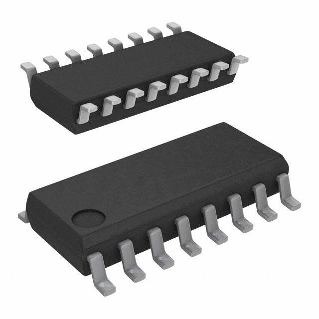
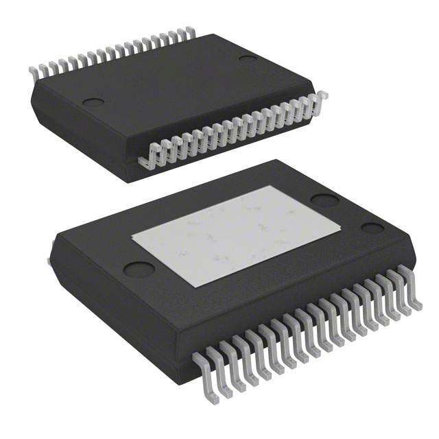
| 描述 | IC QUAD DIFF PECL RCVR 16-SOICLVDS 接口集成电路 QUAD PECL RECEIVER |
| 产品分类 | |
| 品牌 | Texas Instruments |
| 产品手册 | |
| 产品图片 |
|
| rohs | 符合RoHS无铅 / 符合限制有害物质指令(RoHS)规范要求 |
| 产品系列 | 接口 IC,LVDS 接口集成电路,Texas Instruments TB5R3D- |
| 数据手册 | |
| 产品型号 | TB5R3D |
| 产品目录页面 | |
| 产品种类 | LVDS 接口集成电路 |
| 供应商器件封装 | 16-SOIC N |
| 其它名称 | 296-19322-5 |
| 包装 | 管件 |
| 协议 | - |
| 单位重量 | 155.100 mg |
| 双工 | - |
| 商标 | Texas Instruments |
| 安装类型 | 表面贴装 |
| 安装风格 | SMD/SMT |
| 封装 | Tube |
| 封装/外壳 | 16-SOIC(0.154",3.90mm 宽) |
| 封装/箱体 | SOIC-16 |
| 工作温度 | -40°C ~ 85°C |
| 工作电源电压 | 5 V |
| 工厂包装数量 | 40 |
| 接收器滞后 | 50mV |
| 接收机数量 | 4 Receiver |
| 数据速率 | - |
| 最大工作温度 | + 85 C |
| 最小工作温度 | - 40 C |
| 标准包装 | 40 |
| 电压-电源 | 4.5 V ~ 5.5 V |
| 电源电压-最大 | 5.5 V |
| 电源电压-最小 | 4.5 V |
| 类型 | 接收器 |
| 系列 | TB5R3 |
| 输出类型 | TTL |
| 驱动器/接收器数 | 0/4 |


- 商务部:美国ITC正式对集成电路等产品启动337调查
- 曝三星4nm工艺存在良率问题 高通将骁龙8 Gen1或转产台积电
- 太阳诱电将投资9.5亿元在常州建新厂生产MLCC 预计2023年完工
- 英特尔发布欧洲新工厂建设计划 深化IDM 2.0 战略
- 台积电先进制程称霸业界 有大客户加持明年业绩稳了
- 达到5530亿美元!SIA预计今年全球半导体销售额将创下新高
- 英特尔拟将自动驾驶子公司Mobileye上市 估值或超500亿美元
- 三星加码芯片和SET,合并消费电子和移动部门,撤换高东真等 CEO
- 三星电子宣布重大人事变动 还合并消费电子和移动部门
- 海关总署:前11个月进口集成电路产品价值2.52万亿元 增长14.8%


PDF Datasheet 数据手册内容提取
TB5R3 www.ti.com SLLS643A–SEPTEMBER2005–REVISEDOCTOBER2007 QUAD DIFFERENTIAL PECL RECEIVERS FEATURES 1 • FunctionalReplacementfortheAgereBRF1A DESCRIPTION • PinEquivalenttoGeneralTrade26LS32 These quad differential receivers accept digital data • HighInputImpedanceApproximately8kΩ over balanced transmission lines. They translate differential input logic levels to TTL output logic • <2.6-nsMaximumPropagationDelay levels. • TB5R3Provides50-mVHysteresis(Typical) The TB5R3 is a pin- and function-compatible • -1.1-Vto7.1-VCommon-ModeInputVoltage replacement for the Agere systems BRF1A; it Range includes3-kVHBMand2-kVCDMESDprotection. • Single5-V±10%Supply The power-down loading characteristics of the • ESDProtectionHBM>3kVandCDM>2kV receiver input circuit are approximately 8 kΩ relative • OperatingTemperatureRange:-40(cid:176) Cto85(cid:176) C to the power supplies; hence they do not load the • AvailableinGull-WingSOIC(JEDECMS-013, transmissionlinewhenthecircuitispowereddown. DW)andSOIC(D)Package The packaging for this differential line receiver is a 16-pingullwingSOIC(DW)ora16pinSOIC(D). APPLICATIONS The enable inputs of this device include internal • DigitalDataorClockTransmissionOver pull-up resistors of approximately 40 kΩ that are BalancedLines connected to V to ensure a logical high level input CC iftheinputsareopencircuited. FUNCTIONALBLOCKDIAGRAM PIN ASSIGNMENTS AI SOIC PACKAGE AO (TOP VIEW) AAII BI AI 1 16 VCC BI BO AI 2 15 DI C1 AO 3 14 DI CO C1 E1 4 13 DO DD11 BO 5 12 E2 DO D1 BI 6 11 CO E1 BI 7 10 CI E2 GND 8 9 CI Enable Truth Table OUTPUT E1 E2 CONDITION 0 0 Active 1 0 Active 0 1 Disabled 1 1 Active 1 Pleasebeawarethatanimportantnoticeconcerningavailability,standardwarranty,anduseincriticalapplicationsof TexasInstrumentssemiconductorproductsanddisclaimerstheretoappearsattheendofthisdatasheet. PRODUCTIONDATAinformationiscurrentasofpublicationdate. Copyright©2005–2007,TexasInstrumentsIncorporated Products conform to specifications per the terms of the Texas Instruments standard warranty. Production processing does not necessarilyincludetestingofallparameters.
TB5R3 www.ti.com SLLS643A–SEPTEMBER2005–REVISEDOCTOBER2007 Thesedeviceshavelimitedbuilt-inESDprotection.Theleadsshouldbeshortedtogetherorthedeviceplacedinconductivefoam duringstorageorhandlingtopreventelectrostaticdamagetotheMOSgates. ORDERINGINFORMATION PARTNUMBER(1) PARTMARKING PACKAGE(2) LEADFINISH STATUS TB5R3DW TB5R3 Gull-WingSOIC NiPdAu Production TB5R3D TB5R3 SOIC NiPdAu Production (1) AddtheRsuffixfortapeandreelcarrier(i.e.,TB5R3DR) (2) Forthemostcurrentpackageandorderinginformation,seethePackageOptionAddendumattheendofthisdocument,orseetheTI websiteatwww.ti.com. POWER DISSIPATION RATINGS THERMALRESISTANCE, DERATING PACKAGE CIRCMUOITDBEOLARD POWTAER≤2R5A(cid:176) CTING JUWNICTTHIONNO-TAOIR-AFMLBOIEWNT FTAC≥T2O5R(cid:176) C(1) POWTAER=8R5A(cid:176) CTING A Low-K(2) 831mW 120.3(cid:176) C/W 8.3mW/(cid:176) C 332mW DW High-K(3) 1240mW 80.8(cid:176) C/W 12.4mW/(cid:176) C 494mW Low-K(2) 763mW 131.1(cid:176) C/W 7.6mW/(cid:176) C 305mW D High-K(3) 1190mW 84.1(cid:176) C/W 11.9mW/(cid:176) C 475mW (1) Thisistheinverseofthejunction-to-ambientthermalresistancewhenboard-mountedwithnoairflow. (2) Inaccordancewiththelow-KthermalmetricdefinitionsofEIA/JESD51-3. (3) Inaccordancewiththehigh-KthermalmetricdefinitionsofEIA/JESD51-7. THERMAL CHARACTERISTICS PARAMETER PACKAGE VALUE UNIT DW 53.7 q Junction-to-BoardThermalResistance (cid:176) C/W JB D 47.5 DW 47.1 q Junction-to-CaseThermalResistance (cid:176) C/W JC D 44.2 ABSOLUTE MAXIMUM RATINGS overoperatingfree-airtemperaturerangeunlessotherwisenoted(1) UNIT Supplyvoltage,V 0Vto6V CC Magnitudeofdifferentialbus(input)voltage,|V -V |,|V -V |,|V -V |,|V -V | 8.4V AI AI BI BI CI CI DI DI HumanBodyModel(2) Allpins ±3.5kV ESD Charged-DeviceModel(3) Allpins ±2kV Continuouspowerdissipation SeeDissipationRatingTable Storagetemperature,T -65(cid:176) Cto150(cid:176) C stg (1) Stressesbeyondthoselistedunder"absolutemaximumratings”maycausepermanentdamagetothedevice.Thesearestressratings only,andfunctionaloperationofthedeviceattheseoranyotherconditionsbeyondthoseindicatedunder"recommendedoperating conditions”isnotimplied.Exposuretoabsolute-maximum-ratedconditionsforextendedperiodsmayaffectdevicereliability. (2) TestedinaccordancewithJEDECStandard22,TestMethodA114-A. (3) TestedinaccordancewithJEDECStandard22,TestMethodC101. 2 SubmitDocumentationFeedback Copyright©2005–2007,TexasInstrumentsIncorporated ProductFolderLink(s):TB5R3
TB5R3 www.ti.com SLLS643A–SEPTEMBER2005–REVISEDOCTOBER2007 RECOMMENDED OPERATING CONDITIONS MIN NOM MAX UNIT Supplyvoltage,V 4.5 5 5.5 V CC Buspininputvoltage,V ,V ,V V ,V ,orV ,V ,V -1.2(1) 7.2 V AI AI BI BI CI CI DI DI Magnitudeofdifferentialinputvoltage,|V -V |,|V -V |,|V -V |,|V -V | 0.1 6 V AI AI BI BI CI CI DI DI Low-levelenableinputvoltage(2),V (V =5.5V) 0.8 V IL CC High-levelenableinputvoltage(2),V (V =5.5V) 2 V IH CC Operatingfree-airtemperature,T -40 85 (cid:176) C A (1) Thealgebraicconvention,inwhichtheleastpositive(mostnegative)limitisdesignatedasminimumisusedinthisdatasheet,unless otherwisenoted. (2) Theinputlevelsanddifferencevoltageprovidenonoiseimmunityandshouldbetestedonlyinastatic,noise-freeenvironment. DEVICE ELECTRICAL CHARACTERISTICS overoperatingfree-airtemperaturerangeunlessotherwisenoted PARAMETER TESTCONDITIONS MIN TYP MAX UNIT Outputsdisabled 50 mA I Supplycurrent(1) CC Outputsenabled 48 mA (1) CurrentisdcpowerdrawasmeasuredthroughGNDpinanddoesnotincludepowerdeliveredtoload. RECEIVER ELECTRICAL CHARACTERISTICS overoperatingfree-airtemperaturerangeunlessotherwisenoted PARAMETER TESTCONDITIONS MIN TYP MAX UNIT V Outputlowvoltage V =4.5V, I =8mA 0.4 V OL CC OL V Outputhighvoltage V =4.5V, I =-400µA 2.4 V OH CC OH V Enableinputclampvoltage V =4.5V, I =-5mA -1(1) V IK CC I V Positive-goingdifferentialinputthresholdvoltage(2),(V -V ) x=A,B,C,orD 100 mV TH+ xl xI VTH- Negative-goingdifferentialinputthresholdvoltage(2),(Vxl-VxI) x=A,B,C,orD 100(1-) mV V Differentialinputthresholdvoltagehysteresis,(V -V ) 50 mV HYST TH+ TH– I V =0.4V -20(1) µA OZL O Outputoff-statecurrent,(High-Z) V =5.5V CC I V =2.4V 20 µA OZH O - IOS Outputshortcircuitcurrent VCC=5.5V 400(1) mA - IIL Enableinputlowcurrent VCC=5.5V, VIN=0.4V 400(1) µA Enableinputhighcurrent V =2.7V 20 µA IN I V =5.5V IH CC Enableinputreversecurrent V =5.5V 100 µA IN I Differentialinputlowcurrent V =5.5V, V =-1.2V -2(1) mA IL CC IN I Differentialinputhighcurrent V =5.5V, V =7.2V 1 mA IH CC IN OutputHigh 50 R Small-signaloutputresistance Ω O OutputLow 25 (1) Thisparameterislistedusingamagnitudeandpolarity/directionconvention,ratherthananalgebraicconvention,tomatchtheoriginal Ageredatasheet. (2) Theinputlevelsanddifferencevoltageprovidenonoiseimmunityandshouldbetestedonlyinastatic,noise-freeenvironment. Copyright©2005–2007,TexasInstrumentsIncorporated SubmitDocumentationFeedback 3 ProductFolderLink(s):TB5R3
TB5R3 www.ti.com SLLS643A–SEPTEMBER2005–REVISEDOCTOBER2007 SWITCHING CHARACTERISTICS overoperatingfree-airtemperaturerangeunlessotherwisenoted PARAMETER TESTCONDITIONS MIN TYP MAX UNIT tPLH Propagationdelaytime,low-to-high-leveloutput CL=0pF(1), 1.64 <2.6 ns t Propagationdelaytime,high-to-low-leveloutput SeeFigure2andFigure4 1.57 <2.6 PHL t Propagationdelaytime,low-to-high-leveloutput 2.2 3.5 PLH C =50pF,SeeFigure2andFigure4(2) ns L t Propagationdelaytime,high-to-low-leveloutput 2.1 3.5 PHL Outputdisabletime,high-level-to-high-impedance tPHZ output(3) 7.7 12 ns C =5pF,SeeFigure3andFigure5 L Outputdisabletime,low-level-to-high-impedance tPLZ output(3) 5.2 12 ns C =10pF,SeeFigure2andFigure4 0.7 ns L t Pulse-widthdistortion,|t -t | skew1 PHL PLH C =150pF,SeeFigure2andFigure4 4 ns L C =10pF,T =75(cid:176) C,SeeFigure2and Δtskew1p Part-to-partoutputwaveformskew FiLgure4 A 0.8 1.4 ns -p C =10pF,SeeFigure2andFigure4 1.5 ns L Δt Samepartoutputwaveformskew C =10pF,SeeFigure2andFigure4 0.3 ns skew L Outputenabletime,high-impedance-to-high-level tPZH output(3) 6.9 12 ns C =10pF,SeeFigure3andFigure4 L Outputenabletime,high-impedance-to-low-level tPZL output(3) 6.3 12 ns t Risetime(20%-80%) 1 ns TLH C =10pF,SeeFigure2andFigure4 L t Falltime(80%-20%) 1 ns THL (1) Thepropagationdelayvalueswitha0pFloadarebasedondesignandsimulation. (2) t/t:3ns(20%-80%) r f (3) SeeTable1. See Note A See Note A t t f r 3.7 V INPUT 80% 80% 3.2 V 20% 20% INPUT 2.7 V t t PHL PLH OUTPUT VOH 80% 80% 1.5 V 20% 20% VOL t t THL TLH A. t/t:3ns(20%-80%) r f Figure1.ReceiverPropagationDelayTimes 4 SubmitDocumentationFeedback Copyright©2005–2007,TexasInstrumentsIncorporated ProductFolderLink(s):TB5R3
TB5R3 www.ti.com SLLS643A–SEPTEMBER2005–REVISEDOCTOBER2007 E2 2.4 V See Note A 1.5 V 0.4 V 2.4 V E1 1.5 V See Note B 0.4 V t t t t PHZ PZH PLZ PZL VOH OUTPUT VOL 0.2 V 0.2 V 0.2 V 0.2 V A. E2=1whileE1changesstates. B. E1=0whileE2changesstates. Figure2.ReceiverEnableandDisableTiming Parametric values specified under the Electrical Characteristics and Timing Characteristics sections for the data transmissiondriverdevicesaremeasuredwiththefollowingoutputloadcircuits. 5 V TO OUTPUT 2 k OF DEVICE DIODES TYPE UNDER TEST CL 5 k 458E, 1N4148, OR EQUIVALENT C includes test-fixture and probe capacitance. L Figure3.ReceiverPropagationDelayTimeandEnableTime(t ,t )TestCircuit PZH PZL TO OUTPUT 500(cid:1) OF DEVICE 1.5 V UNDER TEST C L C includes test-fixture and probe capacitance. L Figure4.ReceiverDisableTime(t ,t )TestCircuit PHZ PLZ Copyright©2005–2007,TexasInstrumentsIncorporated SubmitDocumentationFeedback 5 ProductFolderLink(s):TB5R3
TB5R3 www.ti.com SLLS643A–SEPTEMBER2005–REVISEDOCTOBER2007 TYPICAL CHARACTERISTICS TYPICALPROPAGATIONDELAY vs LOADCAPACITANCE 4 3.5 s n e − 3 tPLH m y Ti 2.5 tPHL a el D n 2 o ati ag 1.5 p o r P − 1 d p t 0.5 0 0 25 50 75 100 125 150 175 200 225 CL − Load Capacitance − pF NOTE: Thisgraphisincludedasanaidtothesystemdesigners.Totalcircuitdelayvarieswithloadcapacitance.Thetotaldelayis the sumofthedelayduetoexternalcapacitanceandtheintrinsicdelayofthedevice.Intrinsicdelayislistedinthetableaboveasthe0 pF load condition. The incremental increase in delay between the 0 pF load condition and the actual total load capacitance representstheextrinsic,orexternaldelaycontributedbytheload. Figure5. 6 SubmitDocumentationFeedback Copyright©2005–2007,TexasInstrumentsIncorporated ProductFolderLink(s):TB5R3
TB5R3 www.ti.com SLLS643A–SEPTEMBER2005–REVISEDOCTOBER2007 TYPICAL CHARACTERISTICS (continued) LOW-TO-HIGHPROPAGATIONDELAY HIGH-TO-LOWPROPAGATIONDELAY vs vs JUNCTIONTEMPERATURE JUNCTIONTEMPERATURE 2.5 2.5 VCC = 5 V VCC = 5 V, ns Loaded per Figure 3 ns Loaded per Figure 3 − Max − ay 2 ay 2 Max el el D D n Typ n Typ o o gati 1.5 gati 1.5 a a p p o o h Pr Min w Pr Min Hig 1 Lo 1 o- o- w-t h-t − Lo 0.5 − HigL 0.5 H H L P P t t 0 0 −50 −25 0 25 50 75 100 125 150 175 −50 −25 0 25 50 75 100 125 150 175 TJ − Junction Temperature − (cid:1)C TJ − Junction Temperature − (cid:1)C Figure6. Figure7. MINIMUMV ANDMAXIMUMV TYPICALANDMAXIMUMI OH OL CC vs vs JUNCTIONTEMPERATURE JUNCTIONTEMPERATURE 4 50 VCC = 5.5 V 45 3.5 VOH, min VOH, min 40 3 A ge − V 2.5 nt − m 35 ut Volta 2 VLoCaCd =e 4d. 5p eVr, Figure 3 y Curre 2350 VOL, max V− Outp O 1.5 − Suppl C 1250 1 IC 10 0.5 VOL, max 5 0 0 −50 −25 0 25 50 75 100 125 150 175 −50 −25 0 25 50 75 100 125 150 175 TJ − Junction Temperature − (cid:1)C TJ − Junction Temperature − (cid:1)C Figure8. Figure9. Copyright©2005–2007,TexasInstrumentsIncorporated SubmitDocumentationFeedback 7 ProductFolderLink(s):TB5R3
TB5R3 www.ti.com SLLS643A–SEPTEMBER2005–REVISEDOCTOBER2007 APPLICATION INFORMATION which the device is mounted and on the airflow over Power Dissipation the device and PCB. JEDEC/EIA has defined standardized test conditions for measuring q . Two The power dissipation rating, often listed as the JA commonly used conditions are the low-K and the package dissipation rating, is a function of the high-K boards, covered by EIA/JESD51-3 and ambient temperature, T , and the airflow around the A EIA/JESD51-7 respectively. Figure 10 shows the device. This rating correlates with the device's low-K and high-K values of q versus air flow for this maximum junction temperature, sometimes listed in JA deviceanditspackageoptions. the absolute maximum ratings tables. The maximum junction temperature accounts for the processes and The standardized q values may not accurately JA materials used to fabricate and package the device, represent the conditions under which the device is inadditiontothedesiredlifeexpectancy. used. This can be due to adjacent devices acting as heat sources or heat sinks, to nonuniform airflow, or There are two common approaches to estimating the to the system PCB having significantly different internal die junction temperature, T . In both of these J thermal characteristics than the standardized test methods, the device internal power dissipation P D PCBs. The second method of system thermal needs to be calculated This is done by totaling the analysis is more accurate. This calculation uses the supply power(s) to arrive at the system power power dissipation and ambient temperature, along dissipation: withtwodeviceandtwosystem-levelparameters: (cid:4)(cid:2)VSn(cid:1)ISn(cid:3) (1) • q JC, the junction-to-case thermal resistance, in degreesCelsiusperwatt and then subtracting the total power dissipation of the • q , the junction-to-board thermal resistance, in externalload(s): JB degreesCelsiusperwatt (cid:2) (V (cid:1)I ) • q , the case-to-ambient thermal resistance, in Ln Ln (2) CA degreesCelsiusperwatt The first TJ calculation uses the power dissipation • q , the board-to-ambient thermal resistance, in BA and ambient temperature, along with one parameter: degreesCelsiusperwatt. q , the junction-to-ambient thermal resistance, in JA degreesCelsiusperwatt. In this analysis, there are two parallel paths, one through the case (package) to the ambient, and The product of P and q is the junction temperature D JA another through the device to the PCB to the riseabovetheambienttemperature.Therefore: ambient. The system-level junction-to-ambient TJ(cid:3)TA(cid:2)(cid:4)PD(cid:1)(cid:1)JA(cid:5) (3) thermal impedance, q JA(S), is the equivalent parallel impedanceofthetwoparallelpaths: 140 TJ(cid:3)TA(cid:2)(cid:4)PD(cid:1)(cid:1)JA(S)(cid:5) (4) where W 120 D, Low−K (cid:1) (cid:4)(cid:6)(cid:1)JC(cid:2)(cid:1)CA(cid:7)(cid:1)(cid:6)(cid:1)JB(cid:2)(cid:1)BA(cid:7)(cid:5) − C/ DW, Low−K JA(S)(cid:3) (cid:6)(cid:1)JC(cid:2)(cid:1)CA(cid:2)(cid:1)JB(cid:2)(cid:1)BA(cid:7) (5) nce 100 The device parameters q and q account for the a JC JB d internal structure of the device. The system-level e mp parameters q and q take into account details of CA BA al I 80 the PCB construction, adjacent electrical and m Ther DW, High−K mcoencdhitaionnicsalinccluodminpgonaeirnfltosw,. Fainnditetehleemeenntv(irFoEn)m,efinnittael 60 D, High−K difference (FD), or computational fluid dynamics (CFD) programs can determine q and q . Details CA BA on using these programs are beyond the scope of this data sheet, but are available from the software 40 0 100 200 300 400 500 manufacturers. Figure10.ThermalImpedancevsAirFlow Note that q is highly dependent on the PCB on JA 8 SubmitDocumentationFeedback Copyright©2005–2007,TexasInstrumentsIncorporated ProductFolderLink(s):TB5R3
PACKAGE OPTION ADDENDUM www.ti.com 6-Feb-2020 PACKAGING INFORMATION Orderable Device Status Package Type Package Pins Package Eco Plan Lead/Ball Finish MSL Peak Temp Op Temp (°C) Device Marking Samples (1) Drawing Qty (2) (6) (3) (4/5) TB5R3DW ACTIVE SOIC DW 16 40 Green (RoHS NIPDAU Level-1-260C-UNLIM -40 to 85 TB5R3 & no Sb/Br) (1) The marketing status values are defined as follows: ACTIVE: Product device recommended for new designs. LIFEBUY: TI has announced that the device will be discontinued, and a lifetime-buy period is in effect. NRND: Not recommended for new designs. Device is in production to support existing customers, but TI does not recommend using this part in a new design. PREVIEW: Device has been announced but is not in production. Samples may or may not be available. OBSOLETE: TI has discontinued the production of the device. (2) RoHS: TI defines "RoHS" to mean semiconductor products that are compliant with the current EU RoHS requirements for all 10 RoHS substances, including the requirement that RoHS substance do not exceed 0.1% by weight in homogeneous materials. Where designed to be soldered at high temperatures, "RoHS" products are suitable for use in specified lead-free processes. TI may reference these types of products as "Pb-Free". RoHS Exempt: TI defines "RoHS Exempt" to mean products that contain lead but are compliant with EU RoHS pursuant to a specific EU RoHS exemption. Green: TI defines "Green" to mean the content of Chlorine (Cl) and Bromine (Br) based flame retardants meet JS709B low halogen requirements of <=1000ppm threshold. Antimony trioxide based flame retardants must also meet the <=1000ppm threshold requirement. (3) MSL, Peak Temp. - The Moisture Sensitivity Level rating according to the JEDEC industry standard classifications, and peak solder temperature. (4) There may be additional marking, which relates to the logo, the lot trace code information, or the environmental category on the device. (5) Multiple Device Markings will be inside parentheses. Only one Device Marking contained in parentheses and separated by a "~" will appear on a device. If a line is indented then it is a continuation of the previous line and the two combined represent the entire Device Marking for that device. (6) Lead/Ball Finish - Orderable Devices may have multiple material finish options. Finish options are separated by a vertical ruled line. Lead/Ball Finish values may wrap to two lines if the finish value exceeds the maximum column width. Important Information and Disclaimer:The information provided on this page represents TI's knowledge and belief as of the date that it is provided. TI bases its knowledge and belief on information provided by third parties, and makes no representation or warranty as to the accuracy of such information. Efforts are underway to better integrate information from third parties. TI has taken and continues to take reasonable steps to provide representative and accurate information but may not have conducted destructive testing or chemical analysis on incoming materials and chemicals. TI and TI suppliers consider certain information to be proprietary, and thus CAS numbers and other limited information may not be available for release. In no event shall TI's liability arising out of such information exceed the total purchase price of the TI part(s) at issue in this document sold by TI to Customer on an annual basis. Addendum-Page 1
GENERIC PACKAGE VIEW DW 16 SOIC - 2.65 mm max height 7.5 x 10.3, 1.27 mm pitch SMALL OUTLINE INTEGRATED CIRCUIT This image is a representation of the package family, actual package may vary. Refer to the product data sheet for package details. 4224780/A www.ti.com
PACKAGE OUTLINE DW0016A SOIC - 2.65 mm max height SCALE 1.500 SOIC C 10.63 SEATING PLANE TYP 9.97 A PIN 1 ID 0.1 C AREA 14X 1.27 16 1 10.5 2X 10.1 8.89 NOTE 3 8 9 0.51 16X 0.31 7.6 B 7.4 0.25 C A B 2.65 MAX NOTE 4 0.33 TYP 0.10 SEE DETAIL A 0.25 GAGE PLANE 0.3 0 - 8 0.1 1.27 0.40 DETAIL A (1.4) TYPICAL 4220721/A 07/2016 NOTES: 1. All linear dimensions are in millimeters. Dimensions in parenthesis are for reference only. Dimensioning and tolerancing per ASME Y14.5M. 2. This drawing is subject to change without notice. 3. This dimension does not include mold flash, protrusions, or gate burrs. Mold flash, protrusions, or gate burrs shall not exceed 0.15 mm, per side. 4. This dimension does not include interlead flash. Interlead flash shall not exceed 0.25 mm, per side. 5. Reference JEDEC registration MS-013. www.ti.com
EXAMPLE BOARD LAYOUT DW0016A SOIC - 2.65 mm max height SOIC 16X (2) SEE SYMM DETAILS 1 16 16X (0.6) SYMM 14X (1.27) 8 9 R0.05 TYP (9.3) LAND PATTERN EXAMPLE SCALE:7X METAL SOLDER MASK SOLDER MASK METAL OPENING OPENING 0.07 MAX 0.07 MIN ALL AROUND ALL AROUND NON SOLDER MASK SOLDER MASK DEFINED DEFINED SOLDER MASK DETAILS 4220721/A 07/2016 NOTES: (continued) 6. Publication IPC-7351 may have alternate designs. 7. Solder mask tolerances between and around signal pads can vary based on board fabrication site. www.ti.com
EXAMPLE STENCIL DESIGN DW0016A SOIC - 2.65 mm max height SOIC 16X (2) SYMM 1 16 16X (0.6) SYMM 14X (1.27) 8 9 R0.05 TYP (9.3) SOLDER PASTE EXAMPLE BASED ON 0.125 mm THICK STENCIL SCALE:7X 4220721/A 07/2016 NOTES: (continued) 8. Laser cutting apertures with trapezoidal walls and rounded corners may offer better paste release. IPC-7525 may have alternate design recommendations. 9. Board assembly site may have different recommendations for stencil design. www.ti.com
IMPORTANTNOTICEANDDISCLAIMER TI PROVIDES TECHNICAL AND RELIABILITY DATA (INCLUDING DATASHEETS), DESIGN RESOURCES (INCLUDING REFERENCE DESIGNS), APPLICATION OR OTHER DESIGN ADVICE, WEB TOOLS, SAFETY INFORMATION, AND OTHER RESOURCES “AS IS” AND WITH ALL FAULTS, AND DISCLAIMS ALL WARRANTIES, EXPRESS AND IMPLIED, INCLUDING WITHOUT LIMITATION ANY IMPLIED WARRANTIES OF MERCHANTABILITY, FITNESS FOR A PARTICULAR PURPOSE OR NON-INFRINGEMENT OF THIRD PARTY INTELLECTUAL PROPERTY RIGHTS. These resources are intended for skilled developers designing with TI products. You are solely responsible for (1) selecting the appropriate TI products for your application, (2) designing, validating and testing your application, and (3) ensuring your application meets applicable standards, and any other safety, security, or other requirements. These resources are subject to change without notice. TI grants you permission to use these resources only for development of an application that uses the TI products described in the resource. Other reproduction and display of these resources is prohibited. No license is granted to any other TI intellectual property right or to any third party intellectual property right. TI disclaims responsibility for, and you will fully indemnify TI and its representatives against, any claims, damages, costs, losses, and liabilities arising out of your use of these resources. TI’s products are provided subject to TI’s Terms of Sale (www.ti.com/legal/termsofsale.html) or other applicable terms available either on ti.com or provided in conjunction with such TI products. TI’s provision of these resources does not expand or otherwise alter TI’s applicable warranties or warranty disclaimers for TI products. Mailing Address: Texas Instruments, Post Office Box 655303, Dallas, Texas 75265 Copyright © 2020, Texas Instruments Incorporated