ICGOO在线商城 > Si3500-A-GM
 Datasheet下载
- 型号: Si3500-A-GM
- 制造商: Silicon Laboratories
- 库位|库存: xxxx|xxxx
- 要求:
| 数量阶梯 | 香港交货 | 国内含税 |
| +xxxx | $xxxx | ¥xxxx |
查看当月历史价格
查看今年历史价格
Si3500-A-GM产品简介:
ICGOO电子元器件商城为您提供Si3500-A-GM由Silicon Laboratories设计生产,在icgoo商城现货销售,并且可以通过原厂、代理商等渠道进行代购。 提供Si3500-A-GM价格参考以及Silicon LaboratoriesSi3500-A-GM封装/规格参数等产品信息。 你可以下载Si3500-A-GM参考资料、Datasheet数据手册功能说明书, 资料中有Si3500-A-GM详细功能的应用电路图电压和使用方法及教程。
Silicon Labs 的 SI3500-A-GM 是一款高效、同步降压型 DC-DC 开关稳压器,广泛应用于对电源效率和空间布局要求较高的电子设备中。其典型应用场景包括工业自动化控制、物联网(IoT)网关设备、智能家居控制器以及便携式工业仪表等。该器件支持宽输入电压范围,能够在不同供电条件下稳定工作,适用于由电池或直流电源供电的系统。

SI3500-A-GM 具有高集成度和小封装(如QFN),适合空间受限的应用,例如紧凑型传感器节点和无线通信模块。其高效的能量转换特性有助于降低功耗和发热,延长电池寿命,特别适用于需要长时间运行的低功耗设备。此外,该稳压器具备良好的瞬态响应和输出电压精度,可为微处理器、FPGA、传感器和射频模块等提供稳定的电源。

在通信基础设施中,SI3500-A-GM 可用于为小型基站、网络接入设备中的数字电路供电。由于其具备过温保护、过流保护等安全功能,也适用于可靠性要求较高的工业环境。总体而言,SI3500-A-GM 凭借其高效率、小尺寸和高可靠性,成为现代嵌入式系统和智能设备中理想的电源管理解决方案。
| 参数 | 数值 |
| 产品目录 | 集成电路 (IC)半导体 |
| 描述 | IC REG BUCK ADJ 0.4A 20QFN稳压器—开关式稳压器 -57V to +3.3V DC/DC Converter-PSE Supply |
| 产品分类 | |
| 品牌 | Silicon Laboratories IncSilicon Labs |
| 产品手册 | |
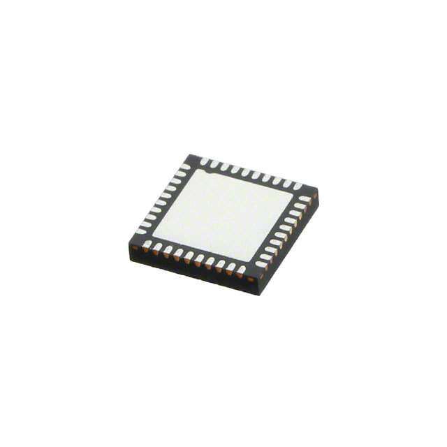
| 产品图片 |
|
| rohs | 符合RoHS无铅 / 符合限制有害物质指令(RoHS)规范要求 |
| 产品系列 | 电源管理 IC,稳压器—开关式稳压器,Silicon Labs Si3500-A-GM- |
| 数据手册 | |
| 产品型号 | SI3500-A-GMSi3500-A-GM |
| PWM类型 | - |
| 产品种类 | 稳压器—开关式稳压器 |
| 供应商器件封装 | 20-QFN(5x5) |
| 其它名称 | 336-1844-5 |
| 包装 | 托盘 |
| 单位重量 | 61.590 mg |
| 同步整流器 | 无 |
| 商标 | Silicon Labs |
| 安装类型 | 表面贴装 |
| 安装风格 | SMD/SMT |
| 封装 | Tray |
| 封装/外壳 | 20-VQFN 裸露焊盘 |
| 封装/箱体 | QFN-20 |
| 工作温度 | -40°C ~ 85°C |
| 工厂包装数量 | 60 |
| 开关频率 | 350 kHz |
| 最大工作温度 | + 85 C |
| 最大输入电压 | 57 V |
| 最小工作温度 | - 40 C |
| 最小输入电压 | 42 V |
| 标准包装 | 60 |
| 电压-输入 | 42 V ~ 57 V |
| 电压-输出 | 1.8 V ~ 12 V |
| 电流-输出 | 400mA |
| 类型 | Voltage Converter降压(降压) |
| 系列 | Si3500 |
| 输出数 | 1 |
| 输出电流 | 400 mA |
| 输出类型 | 可调式 |
| 配用 | /product-detail/zh/SI3480MS8-KIT/SI3480MS8-KIT-ND/2601692/product-detail/zh/SMARTPSE24-KIT/SMARTPSE24-KIT-ND/2601720 |
| 频率-开关 | 350kHz |


- 商务部:美国ITC正式对集成电路等产品启动337调查
- 曝三星4nm工艺存在良率问题 高通将骁龙8 Gen1或转产台积电
- 太阳诱电将投资9.5亿元在常州建新厂生产MLCC 预计2023年完工
- 英特尔发布欧洲新工厂建设计划 深化IDM 2.0 战略
- 台积电先进制程称霸业界 有大客户加持明年业绩稳了
- 达到5530亿美元!SIA预计今年全球半导体销售额将创下新高
- 英特尔拟将自动驾驶子公司Mobileye上市 估值或超500亿美元
- 三星加码芯片和SET,合并消费电子和移动部门,撤换高东真等 CEO
- 三星电子宣布重大人事变动 还合并消费电子和移动部门
- 海关总署:前11个月进口集成电路产品价值2.52万亿元 增长14.8%


PDF Datasheet 数据手册内容提取
Si3500 50 V INPUT DC TO DC CONVERTER Features Integrated switching regulator Supports non-isolated and controller with on-chip power FET isolated switching topologies Input range 42 to 57V Comprehensive protection circuitry Output can be set from 1.8 to 12V Transient overvoltage protection d Undervoltage lockout Output power up to 10W e Thermal shutdown protection Highly-integrated IC enables Short circuit protection d compact solution footprints 50% duty cycle limiting Minimal external components Low-profile, 5x5mm, 20-pin QnFN s Integrated transient surge RoHS-compliant e Ordering Information: suppressor n Integrated dual current-limited m See Ordering Guide on page hotswap switch g page14. Integrated switching power FET i m s Applications Pin Assignments e o 5x5mm QFN 3.3V power supply generation Internet appliances D (Top View) for Power over Ethernet Power Nectwork devices Sourcing supply, such as Si3452 e B SS2 WO SS1 POSS SSA w F V S V V V Description 20 19 18 17 16 15 R The Si3500 is a highly-integrated, high-voltage (42e to 57V) input dc-to-dc EROUT 1 14 NC converter with integrated PWM control and power FET. The output can be t N SSFT 2 VNEG 13 NC adjusted for various applications in the range of 1.8 to 12VDC. o (PAD) VDD 3 12 VPOSF The integrated hot swap switch provides a 2-level current limit for slow charging of the inpNut filter capacitor forllowed by overcurrent protection at ISOSSFT 4 11 NC 400mA. o 5 6 7 8 9 10 The hot swap switch overcurrent protection fully protects the Si3500 from C S O C G C f N A S N E N short-circuit damage as long as the inductor does not saturate. For RBI H VN situations where it is desirable to use a smaller inductor, it is possible to reduce the overcurrent protection with the addition of one low-cost transistor. The Si3500 can be configured to provide an isolated output voltage or a non-isolated output that is positive or negative with respect to the positive input rail. Input undervoltage and overvoltage lockout functions are fully-integrated. A 65V input clamp is also integrated. Output voltage softstart is enabled by just one capacitor to control the output rise time at startup. Rev. 1.2 1/15 Copyright © 2015 by Silicon Laboratories Si3500
Si3500 Functional Block Diagram T VPOS1 VPOS2 RBIAS VDD ISOSSF SSFT FB EROUT Error SWO Amplifier d PWM Soft e Protection Central Start Bias Control d n s e n VNEG m Si3500 g i m s H V e V V SO oSS SS SS A 1 2 D c e w R e t N o N r o f 2 Rev. 1.2
Si3500 TABLE OF CONTENTS Section Page 1. Electrical Specifications . . . . . . . . . . . . . . . . . . . . . . . . . . . . . . . . . . . . . . . . . . . . . . . . . . .4 2. Typical Application Schematics . . . . . . . . . . . . . . . . . . . . . . . . . . . . . . . . . . . . . . . . . . . . .7 3. Functional Description . . . . . . . . . . . . . . . . . . . . . . . . . . . . . . . . . . . . . . . . . . . . . . . . . . . .9 3.1. Input Surge Protection . . . . . . . . . . . . . . . . . . . . . . . . . . . . . . . . . . . . . . . . . . . . . . . .9 3.2. Under Voltage Lockout . . . . . . . . . . . . . . . . . . . . . . . . . . . . . . . . . . . . . . . . . . . . . . . .9 3.3. Dual Current Limit Hot Swap switch . . . . . . . . . . . . . . . . . . . . . . . . . . . . . . . . . . . . . .9 3.4. Switching Regulator . . . . . . . . . . . . . . . . . . . . . . . . . . . . . .d . . . . . . . . . . . . . . . . . . . .9 3.5. Switcher Startup . . . . . . . . . . . . . . . . . . . . . . . . . . . . . . . . . . . . . . . . . . . . . . . . . . . . .9 e 3.6. Switching Regulator Operation . . . . . . . . . . . . . . . . . . . . . . . . . . . . . . . . . . . . . . . . . .9 4. Layout Guidelines . . . . . . . . . . . . . . . . . . . . . . . . . . . . . . d. . . . . . . . . . . . . . . . . . . . . . . . .10 5. Pin Descriptions . . . . . . . . . . . . . . . . . . . . . . . . . . . . . . . . . . . . . . . . . . . . . . . . . . . . . . . . .11 n s 6. Package Outline . . . . . . . . . . . . . . . . . . . . . . . . . . . . . . . . . . . . . . . . . . . . . . . . . . . . . . . . .13 e 7. Recommended PCB Landing Pattern . . . . . . . . . . . . . . . . . . . . . n. . . . . . . . . . . . . . . . . . .14 8. Ordering Guide . . . . . . . . . . . . . . . . . . . . . . . . m. . . . . . . . . . . . . . . . . . . . . . . . . . . . . . . . . .16 g Document Change List . . . . . . . . . . . . . . . . . . . . . . . . . . . . . . . . . . . . . . . . . . . . . . . . . . . . .17 i Contact Information . . . . . . . . . . . . . . . . . .m . . . . . . . . . . . . s. . . . . . . . . . . . . . . . . . . . . . . . . .18 e o D c e w R e t N o N r o f Rev. 1.2 3
Si3500 1. Electrical Specifications Table 1. Recommended Operating Conditions Description Symbol Min Typ Max Units VPOS – VNEG input voltage VIN 42 — 57 V Ambient Operating Temperature T –40 25 85 °C A Note: Unless otherwise noted, all voltages referenced to VNEG. All minimum and maximum specifications are guaranteed and apply across the recommended operating conditions. Typical values apply at nominal supply voltage and ambient temperature unless otherwise noted. d Table 2. Absolute Maximum Ratings (DC)1 e Type Description d Rating Unit Voltage VPOS n –0.3 to 60 V s HSO e –n0.3 to 60 V m VSS1 or VSS2 g –0.3 to 60 V SWO2 i –0.3 to 60 V m s Current VPOS3 e 0 to 400 mA o VDD D 0 to 2 mA c SWO 0 to 3 A e w VSS1, VSS2, or VSSA 0 to 400 mA R Ambient Storage e –65 to 150 °C Temperature t N Ooperating –40 to 85 °C Notes: N r 1. Unless otherwise noted, all voltages referenced to VNEG. Permanent device damage may occur if the maximum o ratings are exceeded. Functional operation should be restricted to those conditions specified in the operational sections of this data sheetf. Exposure to absolute maximum rating conditions for extended periods may adversely affect device reliability. 2. Averaged over the switching cycle. 3. VPOS is equal to VPOS1 and VPOS2 tied together for test condition purposes. 4 Rev. 1.2
Si3500 Table 3. Absolute Maximum Ratings (Transient)1 Type Description Rating Unit Voltage VPOS2 –0.7 to 80 V HSO –0.7 to 80 V VSS1, VSS2, or VSSA –0.7 to 80 V SWO –0.7 to 80 V Current VPOS2 –5 to 5 A Notes: 1. Unless otherwise noted, all voltages referenced to VNEG. Permanent device damaged may occur if the maximum ratings are exceeded. Functional operation should be restricted to those conditions specified in the operational sections of this data sheet. Exposure to absolute maximum rating conditions for extended perioeds may adversely affect device reliability. d 2. VPOS is equal to VPOS1 and VPOS2 tied together for test condition purposes. n s Table 4. Surge Immunity Ratings1,2 e n Type Description m g Rating Unit ESD (System-Level) Air discharge (IEC 61000-4-2) i –16.5 to 16.5 kV m s Contact discharge (IEC 61000-4-2) –8 to 8 kV e ESD (CDM) JEDEC (JESD22-C101Co) –750 to 750 V D ESD (HBM) JEDEC (JESD22-A1c14E) –2 to 2 kV ESD (MM) JEDEC (JESD2e2-A115A) –150 to 150 V w Notes: R 1. Permanent device damage may occur if the maximum ratings are exceeded. Functional operation should be restricted e to those conditions specified in the operational sections of this data sheet. Exposure to absolute maximum rating conditions for extendted periods may adverNsely affect device reliability. 2. Care should be takoen to follow layout guidelines. N r o f Rev. 1.2 5
Si3500 Table 5. Electrical Characteristics Parameter Description Min Typ Max Unit Inrush — 140 — mA Current Limit1 Operating 400 525 — mA Hotswap FET On-Resistance + 0.5 — 1.5 R SENSE Switcher Frequency — 350 — kHz d Maximum Switcher Duty Cycle ISOSSFT connected to — 50 — % VDD e Switching FET On-Resistance d0.3 — 0.86 Regulated Feedback @ pin FB2 DC Avg. n — 1.23 — V s Regulated Output Voltage Tolerance2 Output voltage toleranece –5 n — 5 % @ VOUT m g VDD accuracy @ 0.8mA 42V < VPOS < 57V 4.5 — 5.5 V i m s Softstart charging current Non-isolated — 25 — µA e oIsolated — 13 — µA D Thermal Shutdown cJunction temperature — 160 — °C e Thermal Shutdown Hysteresis — — 25 °C w R Notes: 1. At turn-on, before the HSO load capacitor is chaerged, the current limit is set at the inrush level. After the capacitor has been charged within ~1 .25V of VNEG, the operating current limit is engaged. This higher current limit remains active until the UVLO lowert limit has been trippedN or until the hotswap switch is sufficiently current-limited to cause a foldback o of the HSO voltage. 2. Applies to non-isolated applications only (VOUT on schematic in Figure1). N r o Table 6. Total Power Dissipation f Description Condition Min Typ Max Units Power Dissipation VIN=50V, VOUT=5V, 2A — 0.7 — W Table 7. Package Thermal Characteristics Parameter Symbol Test Condition Typ Units Thermal resistance Still air; assumes a minimum of 44 °C/W JA (junction to ambient) nine thermal vias are connected to a 2in2 heat spreader plane for the package “pad” node (VNEG). 6 Rev. 1.2
Si3500 2. Typical Application Schematics +VIN +VOUT 50V 3.3 V Cssft 24.9 k POSF SSFT POSS V V FB -Vin RBIAS Cout Si3500 Optional 68µH Hot swap SWO d -VOUT damping VNEG EROUT e O A S S S d H S S V V Cin n Ccomp s e n Figure 1. Schematic (Non-Isolated 3.3 V Output)* m g *Note: This is a simplified schematic. Refer to Si3452 reference design databases for complete application schematic. i m s +VIN 50V e o D2D D1 c D3 OSF OSS SFTe FB T1 R5 P P S w -Vin V V SWO R6 R C8 Optional eISOSSFT PS2911 C3 Hdaomt spwinagp R8 t VNEG Si350N0 VDD R2 Vout o R4 C4 R1 EROUT RBIAS N r R3 C1 foHSO VSS1 VSS2 VSSA C7 C5 TLV431 R7 Figure 2. Schematic (Isolated 3.3 V Output)* *Note: This is a simplified schematic. Refer to Si3452 reference design databases for complete application schematic. Rev. 1.2 7
Si3500 +VIN 50V D1 R8 OSF OSS SFT FB T1 R5 P P S V V SWO R6 C8 ISOSSFT PS2911 C3 V -Vin R1 VNEG Si3500 VDD R2 out R 4 C4 EROUT Optional d to reduce RBIAS Scuhrorretn cti rlicmuiitt EROUT C1 HSO VSS1 VSS2 VSSA C7 CR53 d eTLV431 R7 n s Connect to +Vin e Figure 3. Schematic—Non-Isolated 3.3 V Outpunt* *Note: This is a simplified schematic. Refer to Si3452 reference demsign databases for complete application schematic. g i m s e o D c e w R e t N o N r o Figure 4. Startup Waveform for Current in Figure 3 f 8 Rev. 1.2
Si3500 3. Functional Description 3.4. Switching Regulator The Si3500 can be configured to provide output that is 3.1. Input Surge Protection either more positive, more negative, or isolated from the The Si3500 has a 65V Zener diode clamp on the input positive terminal of the input power supply. between VPOS1 and VNEG. The diode is designed to The application determines the converter topology. An limit the input voltage to less than 80V for surges of up isolated application will require a flyback transformer- to 5A and 50µsec duration. This provides protection based switching topology while a non-isolated against hot plugging the input power supply. application can use an inductor-based buck converter If the input power supply is hot plugged and there is no topology. In the isolated case, dc isolation is achieved surge limiting resistance, there can be an overshoot of through a transformer in the forward path and a voltage input voltage due to lead inductance. For this reason, an reference plus opto-isolator in the feedback path. The optional surge limiting resistor of 2 is recommended. application circuit shown in Figure2 is an example of This is particularly true if EMC reduction capacitor is such a topology. Thed non-isolated application in placed directly across VPOS and VNEG. Figure1 makes use of a single inductor as the energy e conversion element, and the feedback signal is directly 3.2. Under Voltage Lockout supplied into thde internal error amplifier. The approach The Si3500 incorporates an undervoltage lockout shown in Figure3 is for a non-isolated application (UVLO) circuit to monitor the line voltage and determine where the noutput is more positive than the input. s when to activate the integrated switching regulator. 3.5. eSwitcher Startup n Before power is applied to the switching regulator, the hotswap switch output (HSO) pin is high-impedance Thme switching regulator is disabled until the hotswap g and typically follows VPOS as the input is ramped (due interface has charged the supply capacitor needed to to the discharged switcher supply capacitor). When the filter the switchiing regulator's high-current transients. m s input voltage rises above the UVLO turn-on threshold Once the supply capacitor is charged, the hotswap (42V maximum), the Si3500 turns on the internal controller eengages the internal bias currents and hotswap power MOSFET. The switcher supply ocapacitor supplies used by the switcher. Additionally, the soft-start begins to charge up under the current limit control of the curreDnt begins to charge the external soft-start c Si3500, and the HSO pin transitions from VPOS to capacitor. VNEG. The Si3500 includes hysteresise in UVLO circuits The voltage developed across the soft-start capacitor w to maintain power to the load until the input voltage falls serves as the error amplifier's reference in the non- R below the UVLO turn-off threshold. Once the input isolated application. Ramping this voltage slowly allows voltage falls below 30V (minimum), the ineternal the switching regulator to bring up the regulated output hotswap MOSFET is turnetd off. N voltage in a controlled manner. Controlling the initial 3.3. Dual Current Loimit Hot Swap switch startup of the regulated voltage restrains power dissipation in the switching FET and prevents overshoot The Si3500 implemNents dual currenrt limits. While the and ringing in the output supply voltage. hotswap MOSFET is charging the switcher supply o In the isolated mode, a capacitor connected between capacitor, the Si3500 maintains a lower current limit. pins ISOSSFT and VSSA slowly ramps the duty cycle The switching regulator is dfisabled until the voltage clamp in the PWM circuit. Tie the ISOSSFT pin to VDD across the hotswap MOSFET becomes sufficiently low, if not used. indicating the switcher supply capacitor is almost completely charged. When this threshold is reached, 3.6. Switching Regulator Operation the switcher is activated, and the hotswap current limit The switching regulator of the Si3500 is a constant- is increased. This threshold also has hysteresis to frequency, pulse-width-modulated (PWM) controller prevent systemic oscillation as the switcher begins to integrated with switching power FET optimized for the draw current and the current limit is increased. output power range of up to 10W. The Si3500 stays in a high-level current limit mode until Once the hotswap interface has ensured proper turn-on the input voltage drops below the UVLO turn-off of the switching regulator controller, the switcher is fully threshold or excessive power is dissipated in the operational. An internal free-running oscillator and hotswap switch. This dual-level current limit gives low internal precision voltage reference are fed into the current draw from the input power supply during normal pulse-width modulator. The output of the error amplifier start up with the higher current only occurring during (either internal for non-isolated applications or external fault conditions. Rev. 1.2 9
Si3500 for isolated applications) is also routed into the PWM 4. Layout Guidelines and determines the slicing of the oscillator. The following are general PCB layout considerations; The PWM controls the switching FET drive circuitry. A reference designs are also available. Due to the unique significant advantage of integrating the switching power high-voltage and high-power design considerations, FET onto the same monolithic IC as the switching Silicon Labs recommends that the reference designs be regulator controller is the ability to precisely adjust the followed closely for both BOM and layout. Visit the drive strength and timing to the FET's sizable gate, Silicon Labs Technical Support web page and register to resulting in high regulator efficiency. Furthermore, submit a technical support request, particularly if you current-limiting circuitry prevents the switching FET are not closely following the recommended reference from sinking too much current, dissipating too much design. power, and becoming damaged. Thermal overload protection provides a secondary level of protection. Care must be taken to connect the thermal pad of the Si3500 to an appropriate heat spreader. For full-power The flexibility of the Si3500's switching regulator allows d applications, a 2 square in plane with at least 9 thermal the system designer to realize either the isolated or non- vias is recommendeed. This heat spreader must be isolated application circuitry using a single device. In electrically connected to the negative input power operation, the integration of the switching FET allows d supply. tighter control and more efficient operation than a general-purpose switching regulator coupled with a Care mustn also be taken in layout to avoid EMI and s general-purpose external FET. EMC. Input and output filter capacitors are normally e ceramic capacitors for hnigh-frequency performance in parallel with electrolytic capacitors for load transient m g performance. The ceramic capacitors in particular should be placed so as to minimize radiation for the i m high-current spaths of the switching regulator. The circular area of current flow with the FET on and FET off e o should be minimized. The direction of current flow with FET Don and FET off should maintain a constant c clockwise or counterclockwise rotation. e For EMI reduction, a 4 layer design with inner layers w connected to the positive input and Vss (for isolated R applications) or Vout (for non-isolated applications) is e recommended. The high-current paths should not flow through these shield planes. Connection of the dc-to-dc t N converter high-current paths to the shield plane should o be at a single point. Refer to the Si3452 reference N design databases for additional layout guideline details. r o f 10 Rev. 1.2
Si3500 5. Pin Descriptions S B SS2 WO SS1 POS SSA F V S V V V 20 19 18 17 16 15 EROUT 1 14 NC SSFT 2 VNEG 13 NC (PAD) VDD 3 12 VPOSF ISOSSFT 4 11 NC d e 5 6 7 8 9 10 d C S O C G C N A S N E N RBI H VN n s Table 8. Si3500 Pin Descriptieons (Top View) n m Pin# Name Description g 1 EROUT Error-amplifier output and PWM input; directly cionnected to opto-coupler in isolated or m s boost applications. e 2 SSFT Soft-start output pino ramps voltage across external soft-start capacitor to allow switcher to ramp output slowly. D c 3 VDD 5V supply rail for switcher; provides drive for opto-coupler. e w 4 ISOSSFT Isolated mode soft start enable input. Tie to VDD for non-isolated applications. R Connect a 0.1µF capacitor between this pin and VSSA for isolated applications. e 5 NC D o not connect (float). t N 6 RBIAS oA 25.5k resistor connected from this to VPOS sets up the bias currents of the Si3500. N r 7 HSO Hotswap switch output; connects to VNEG through hotswap switch. o 8 NC Do not connect (float). f 9, Pad VNEG Rectified high-voltage supply, negative rail. Must be connected to thermal PAD node (VNEG) on package bottom. This thermal pad must be connected to VNEG (pin #9) as well as a 2in2 heat spreader plane using a minimum of nine thermal vias. 10 NC Do not connect (float). 11 NC Do not connect (float). 12 VPOS1 High-voltage supply, positive rail (force node) 13 NC Do not connect (float). 14 NC Do not connect (float). 15 VSSA Analog ground. Rev. 1.2 11
Si3500 Table 8. Si3500 Pin Descriptions (Top View) (Continued) 16 VPOS2 High-voltage supply, positive rail sense node. 17 VSS1 Negative supply rail for switcher; externally tied to HSO. 18 SWO Switching transistor output; drain of switching N-FET. 19 VSS2 Negative supply rail for switcher; externally tied to HSO. 20 FB Regulated feedback input in non-isolated application. d e d n s e n m g i m s e o D c e w R e t N o N r o f 12 Rev. 1.2
Si3500 6. Package Outline Figure5 illustrates the package details for the Si3500. Table9 lists the values for the dimensions shown in the illustration. d e d n s e n m g i m s Figure 5. 20-Lead Quad Flat No-Lead Package (QFN) e o D Table 9. Package Dimensions c Dimension e Min Nom Max w A 0.80 0.85 0.90 R A1 0.00e 0.02 0.05 b 0.25 0.30 0.35 t N oD 5.00 BSC. N D2 2.60 2.70 2.80 r e o 0.80 BSC. E f 5.00 BSC. E2 2.60 2.70 2.80 L 0.50 0.55 0.60 L1 0.00 — 0.10 aaa — — 0.10 bbb — — 0.10 ccc — — 0.08 ddd — — 0.10 Notes: 1. All dimensions shown are in millimeters (mm) unless otherwise noted. 2. Dimensioning and tolerancing per ANSI Y14.5M-1994. 3. This drawing conforms to the JEDEC Solid State Outline MO-220, Variation VHHB-1. Rev. 1.2 13
Si3500 7. Recommended PCB Landing Pattern d e d n s e n m g i m s e o D c eFigure 6. PCB Land Pattern w R e t N o N r o f 14 Rev. 1.2
Si3500 Table 10. PCB Land Pattern Dimensions Symbol Min Nom Max P1 2.70 2.75 2.80 P2 2.70 2.75 2.80 X1 0.25 0.30 0.35 Y1 0.90 0.95 1.00 C1 4.70 d C2 4.70 e E 0.80 d General: 1. All dimensions shown are in millimeters (mm) unlessn otherwise noted. s 2. Dimensioning and Tolerancing is per the ANSI Y14.5M-1994 specification. 3. This Land Pattern Design is based on the IPC-7e351 guidelines. n Solder Mask Design: m 4. All metal pads are to be non-solder mask defined (NSMD). Cleagrance between the solder mask and the metal pad is to be 60 m minimum, all the way around the pad. Stencil Design: m si 5. A stainless steel, laser-cut and electro-polished stencil with trapezoidal walls should be used to assure good solder paste release. e 6. The stencil thickness shouldo be 0.125mm (5 mils). 7. The ratio of stencil aperture to land pad size shDould be 1:1 for all perimeter pins. 8. A 2x2 array of 1.2 mm scquare openings on 1.4 mm pitch should be used for the center ground pad. e Card Assembly: w 9. A No-Clean, TRype-3 solder paste is recommended. 10. The recommended card reflow profile is per the JEDEC/IPC J-STD-020C specification e for Small Body Components. t N o N r o f Rev. 1.2 15
Si3500 8. Ordering Guide Part Number* Package Temp Range Recommended Maximum Output Power Si3500-A-GM 20-pin QFN, –40 to 85°C < 10W RoHS compliant *Note: Add an “R” at the end of the part number to denote tape and reel option. d e d n s e n m g i m s e o D c e w R e t N o N r o f 16 Rev. 1.2
Si3500 DOCUMENT CHANGE LIST Revision 0.1 to Revision 1.0 Updated revision number to 1.0 to reflect production status. Updated Table4 on page5. Revision 1.0 to Revision 1.1 Editorial changes in "4. Layout Guidelines" on page 10. Revision 1.1 to Revision 1.2 Added “Not Recommended for New Designs” d watermark. e d n s e n m g i m s e o D c e w R e t N o N r o f Rev. 1.2 17
Si3500 CONTACT INFORMATION Silicon Laboratories Inc. 400 West Cesar Chavez Austin, TX 78701 Tel: 1+(512) 416-8500 Fax: 1+(512) 416-9669 Toll Free: 1+(877) 444-3032 Please visit the Silicon Labs Technical Support web page: https://www.siliconlabs.com/support/pages/contacttechnicalsupport.aspx and register to submit a technical support request. d e d n s e n m g i m s e o D c e w R e t N o N r o Patent Notice f Silicon Labs invests in research and development to help our customers differentiate in the market with innovative low-power, small size, analog- intensive mixed-signal solutions. Silicon Labs' extensive patent portfolio is a testament to our unique approach and world-class engineering team. The information in this document is believed to be accurate in all respects at the time of publication but is subject to change without notice. Silicon Laboratories assumes no responsibility for errors and omissions, and disclaims responsibility for any consequences resulting from the use of information included herein. Additionally, Silicon Laboratories assumes no responsibility for the functioning of undescribed fea- tures or parameters. Silicon Laboratories reserves the right to make changes without further notice. Silicon Laboratories makes no warran- ty, representation or guarantee regarding the suitability of its products for any particular purpose, nor does Silicon Laboratories assume any liability arising out of the application or use of any product or circuit, and specifically disclaims any and all liability, including without limitation consequential or incidental damages. Silicon Laboratories products are not designed, intended, or authorized for use in applications intend- ed to support or sustain life, or for any other application in which the failure of the Silicon Laboratories product could create a situation where personal injury or death may occur. Should Buyer purchase or use Silicon Laboratories products for any such unintended or unauthorized application, Buyer shall indemnify and hold Silicon Laboratories harmless against all claims and damages. Silicon Laboratories and Silicon Labs are trademarks of Silicon Laboratories Inc. Other products or brandnames mentioned herein are trademarks or registered trademarks of their respective holders. 18 Rev. 1.2