 Datasheet下载
- 型号: Si3019-F-FS
- 制造商: Silicon Laboratories
- 库位|库存: xxxx|xxxx
- 要求:
| 数量阶梯 | 香港交货 | 国内含税 |
| +xxxx | $xxxx | ¥xxxx |
查看当月历史价格
查看今年历史价格
Si3019-F-FS产品简介:
ICGOO电子元器件商城为您提供Si3019-F-FS由Silicon Laboratories设计生产,在icgoo商城现货销售,并且可以通过原厂、代理商等渠道进行代购。 Si3019-F-FS价格参考。Silicon LaboratoriesSi3019-F-FS封装/规格:接口 - 电信, Telecom IC Direct Access Arrangement (DAA) 16-SOIC。您可以下载Si3019-F-FS参考资料、Datasheet数据手册功能说明书,资料中有Si3019-F-FS 详细功能的应用电路图电压和使用方法及教程。
Silicon Labs 的 SI3019-F-FS 是一款集成的语音数据调制解调器芯片,主要用于电信接口应用。该芯片支持 V.92/V.90 调制解调标准,具备高性能的数据传输和语音处理能力,广泛应用于需要通过传统电话线实现数据通信或语音服务的场景。

其主要应用场景包括:

1. 远程监控与安防系统:用于连接报警主机、摄像头等设备,通过电话网络将报警信息或视频流发送至监控中心或用户手机。

2. 自动抄表系统(AMR):在水表、电表、燃气表等远程抄表设备中,SI3019 可实现通过电话线自动回传数据,提高抄表效率与准确性。

3. 工业控制系统:在偏远地区或无宽带覆盖的环境中,通过 PSTN(公共交换电话网)实现对工业设备的远程控制与状态监测。

4. 医疗监护设备:如远程心电图机、血糖仪等设备,可借助该芯片通过电话网络将患者数据传送到医疗机构。

5. POS 机与支付终端:在部分传统 POS 终端中,仍使用电话线进行交易数据的拨号上传,SI3019 提供稳定可靠的通信保障。

总之,SI3019-F-FS 在各类需通过电话线实现语音与数据通信的应用中具有广泛的适用性,尤其适合于低带宽但高可靠性的远程通信场景。
| 参数 | 数值 |
| 产品目录 | 集成电路 (IC)半导体 |
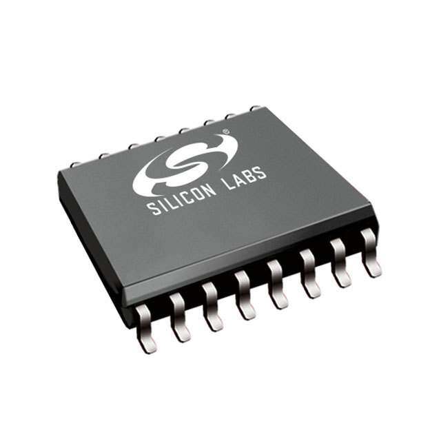
| 描述 | IC LINE-SIDE DAA 16SOIC电信线路管理 IC Si3050 Enhanced Glo Voice DAA Line-Side |
| 产品分类 | |
| 品牌 | Silicon Laboratories IncSilicon Labs |
| 产品手册 | |
| 产品图片 |
|
| rohs | 符合RoHS无铅 / 符合限制有害物质指令(RoHS)规范要求 |
| 产品系列 | 通信及网络 IC,电信线路管理 IC,Silicon Labs Si3019-F-FSISOcap™ |
| 数据手册 | |
| 产品型号 | Si3019-F-FSSI3019-F-FS |
| 产品 | Telecom |
| 产品种类 | 电信线路管理 IC |
| 供应商器件封装 | 16-SOIC N |
| 包装 | 管件 |
| 单位重量 | 189.320 mg |
| 商标 | Silicon Labs |
| 安装类型 | 表面贴装 |
| 安装风格 | SMD/SMT |
| 封装 | Tube |
| 封装/外壳 | 16-SOIC(0.154",3.90mm 宽) |
| 封装/箱体 | SOIC-16 |
| 工作电压 | 3.3 V |
| 工厂包装数量 | 48 |
| 接口类型 | SPI |
| 数据格式 | V.92 |
| 最大工作温度 | + 70 C |
| 最大时钟频率 | 8192 kHz |
| 最小工作温度 | 0 C |
| 标准包装 | 48 |
| 波特率 | - |
| 电压-电源 | 3 V ~ 3.6 V |
| 电源电压-最大 | 3.6 V |
| 电源电压-最小 | 3 V |
| 电源电流 | 8.5 mA |
| 类型 | Telecom IC |
| 系列 | Si3019 |


- 商务部:美国ITC正式对集成电路等产品启动337调查
- 曝三星4nm工艺存在良率问题 高通将骁龙8 Gen1或转产台积电
- 太阳诱电将投资9.5亿元在常州建新厂生产MLCC 预计2023年完工
- 英特尔发布欧洲新工厂建设计划 深化IDM 2.0 战略
- 台积电先进制程称霸业界 有大客户加持明年业绩稳了
- 达到5530亿美元!SIA预计今年全球半导体销售额将创下新高
- 英特尔拟将自动驾驶子公司Mobileye上市 估值或超500亿美元
- 三星加码芯片和SET,合并消费电子和移动部门,撤换高东真等 CEO
- 三星电子宣布重大人事变动 还合并消费电子和移动部门
- 海关总署:前11个月进口集成电路产品价值2.52万亿元 增长14.8%


PDF Datasheet 数据手册内容提取
Si3050+Si3011/18/19 PROGRAMMABLE VOICE DAA SOLUTIONS Features PCM highway data interface TIP/RING polarity detection µ-law/A-law companding Integrated codec and 2- to 4-wire SPI control interface analog hybrid GCI interface Programmable digital hybrid for 80dB dynamic range TX/RX near-end echo reduction Line voltage monitor Polarity reversal detection Loop current monitor Programmable digital gain in 0.1dB +6dBm or +3.2dBm TX/RX level increments mode Integrated ring detector Parallel handset detection Type I and II caller ID support 3µA on-hook line monitor current Pulse dialing support Overload detection 3.3V power supply Programmable line interface Daisy-chaining for up to 16 devices AC termination Greater than 5000V isolation DC termination Patented isolation technology Ground start and loop start support Ring detect threshold Available in Pb-free RoHS-compliant Ordering Information Ringer impedance packages See page106. Applications DSL IADs Voice mail systems Package Options VoIP gateways DECT base stations PBX and IP-PBX systems Si3050 Description SDI SDO NC NC SDITHR SCLK 24 23 22 21 20 19 The Si3050+Si3011/18/19 Voice DAA chipset provides a highly-programmable CS 1 18 GND and globally-compliant foreign exchange office (FXO) analog interface. The FSYNC 2 17 VDD solution implements Silicon Laboratories' patented isolation capacitor technology, PCKLK 3 Si3050 16 VA which eliminates the need for costly isolation transformers, relays, or DTX 4 Top View 15 C1A opto-isolators, while providing superior surge immunity for robust field DRX 5 14 C2A performance. The Voice DAA is available as a chipset, a system-side device GND RGDT 6 13 RESET (Si3050) paired with a line-side device (Si3011/18/19). The Si3050 is available in a 20-pin TSSOP or a 24-pin QFN. The Si3011/18/19 is available in a 16-pin 7 8 9 10 11 12 TcoSmSpOoPn, enat s.1 6T-phien SSOi3I0C5,0 orin tae rfa2c0e-psi n dQireFcNtly antod sretaqnudiraersd mteinleimphaol nye xtePrCnMal AOUT/INT RG NC NC TGD TGDE interfaces. Si3011/18/19 Functional Block Diagram DCT QE DCT2 IGND NC Si3050 Si3018/19 NC 1 20 19 18 17 16 RX 2 15 DCT3 CS RX SCLK Control SDI Data IB IB 3 IGND 14 QB SDI THSDROU Interface THeryambnrdinid aD, tCAioC ns DVSRCCETG C1B 4 PAD 13 QE2 VREG2 PDCTLXK DLiantea IInstoelarftaiocne IInstoelarftaiocne DDCCTT23 C2B 5 12 SC DRX Interface 6 7 8 9 10 11 NC FSYNC Ring Detect RNG1 RTGGRDGDT CLoongtircol Off-Hook QQRQNBEEG22 VREG RNG1 IGND RNG2 VREG2 TGDE RESET US Patent# 5,870,046 AOUT/INT US Patent# 6,061,009 Rev. 1.5 10/11 Copyright © 2011 by Silicon Laboratories Si3050 + Si3011/18/19
Si3050 + Si3011/18/19 2 Rev. 1.5
Si3050 + Si3011/18/19 TABLE OF CONTENTS Section Page 1. Electrical Specifications . . . . . . . . . . . . . . . . . . . . . . . . . . . . . . . . . . . . . . . . . . . . . . . . . . .5 2. Typical Application Schematic . . . . . . . . . . . . . . . . . . . . . . . . . . . . . . . . . . . . . . . . . . . . .17 3. Bill of Materials . . . . . . . . . . . . . . . . . . . . . . . . . . . . . . . . . . . . . . . . . . . . . . . . . . . . . . . . . .19 4. AOUT PWM Output . . . . . . . . . . . . . . . . . . . . . . . . . . . . . . . . . . . . . . . . . . . . . . . . . . . . . . .20 5. Functional Description . . . . . . . . . . . . . . . . . . . . . . . . . . . . . . . . . . . . . . . . . . . . . . . . . . .21 5.1. Line-Side Device Support . . . . . . . . . . . . . . . . . . . . . . . . . . . . . . . . . . . . . . . . . . . . .21 5.2. Power Supplies . . . . . . . . . . . . . . . . . . . . . . . . . . . . . . . . . . . . . . . . . . . . . . . . . . . . .25 5.3. Initialization . . . . . . . . . . . . . . . . . . . . . . . . . . . . . . . . . . . . . . . . . . . . . . . . . . . . . . . .25 5.4. Isolation Barrier . . . . . . . . . . . . . . . . . . . . . . . . . . . . . . . . . . . . . . . . . . . . . . . . . . . . .25 5.5. Power Management . . . . . . . . . . . . . . . . . . . . . . . . . . . . . . . . . . . . . . . . . . . . . . . . .25 5.6. Calibration . . . . . . . . . . . . . . . . . . . . . . . . . . . . . . . . . . . . . . . . . . . . . . . . . . . . . . . . .26 5.7. In-Circuit Testing . . . . . . . . . . . . . . . . . . . . . . . . . . . . . . . . . . . . . . . . . . . . . . . . . . . .26 5.8. Exception Handling . . . . . . . . . . . . . . . . . . . . . . . . . . . . . . . . . . . . . . . . . . . . . . . . . .27 5.9. Revision Identification . . . . . . . . . . . . . . . . . . . . . . . . . . . . . . . . . . . . . . . . . . . . . . . .27 5.10. Transmit/Receive Full-Scale Level . . . . . . . . . . . . . . . . . . . . . . . . . . . . . . . . . . . . .27 5.11. Parallel Handset Detection . . . . . . . . . . . . . . . . . . . . . . . . . . . . . . . . . . . . . . . . . . .27 5.12. Line Voltage/Loop Current Sensing . . . . . . . . . . . . . . . . . . . . . . . . . . . . . . . . . . . .27 5.13. Off-Hook . . . . . . . . . . . . . . . . . . . . . . . . . . . . . . . . . . . . . . . . . . . . . . . . . . . . . . . . .29 5.14. Ground Start Support . . . . . . . . . . . . . . . . . . . . . . . . . . . . . . . . . . . . . . . . . . . . . . .29 5.15. Interrupts . . . . . . . . . . . . . . . . . . . . . . . . . . . . . . . . . . . . . . . . . . . . . . . . . . . . . . . . .30 5.16. DC Termination . . . . . . . . . . . . . . . . . . . . . . . . . . . . . . . . . . . . . . . . . . . . . . . . . . . .31 5.17. AC Termination . . . . . . . . . . . . . . . . . . . . . . . . . . . . . . . . . . . . . . . . . . . . . . . . . . . .31 5.18. Ring Detection . . . . . . . . . . . . . . . . . . . . . . . . . . . . . . . . . . . . . . . . . . . . . . . . . . . . .33 5.19. Ring Validation . . . . . . . . . . . . . . . . . . . . . . . . . . . . . . . . . . . . . . . . . . . . . . . . . . . .34 5.20. Ringer Impedance and Threshold . . . . . . . . . . . . . . . . . . . . . . . . . . . . . . . . . . . . . .34 5.21. Pulse Dialing and Spark Quenching . . . . . . . . . . . . . . . . . . . . . . . . . . . . . . . . . . . .34 5.22. Receive Overload Detection . . . . . . . . . . . . . . . . . . . . . . . . . . . . . . . . . . . . . . . . . .35 5.23. Billing Tone Filter (Optional) . . . . . . . . . . . . . . . . . . . . . . . . . . . . . . . . . . . . . . . . . .35 5.24. On-Hook Line Monitor . . . . . . . . . . . . . . . . . . . . . . . . . . . . . . . . . . . . . . . . . . . . . . .36 5.25. Caller ID . . . . . . . . . . . . . . . . . . . . . . . . . . . . . . . . . . . . . . . . . . . . . . . . . . . . . . . . .36 5.26. Overload Detection . . . . . . . . . . . . . . . . . . . . . . . . . . . . . . . . . . . . . . . . . . . . . . . . .37 5.27. Gain Control . . . . . . . . . . . . . . . . . . . . . . . . . . . . . . . . . . . . . . . . . . . . . . . . . . . . . .38 5.28. Transhybrid Balance . . . . . . . . . . . . . . . . . . . . . . . . . . . . . . . . . . . . . . . . . . . . . . . .38 5.29. Filter Selection . . . . . . . . . . . . . . . . . . . . . . . . . . . . . . . . . . . . . . . . . . . . . . . . . . . .39 5.30. Clock Generation . . . . . . . . . . . . . . . . . . . . . . . . . . . . . . . . . . . . . . . . . . . . . . . . . .39 5.31. Communication Interface Mode Selection . . . . . . . . . . . . . . . . . . . . . . . . . . . . . . .39 5.32. PCM Highway . . . . . . . . . . . . . . . . . . . . . . . . . . . . . . . . . . . . . . . . . . . . . . . . . . . . .40 5.33. Companding in PCM Mode . . . . . . . . . . . . . . . . . . . . . . . . . . . . . . . . . . . . . . . . . . .44 5.34. 16 kHz Sampling Operation in PCM Mode . . . . . . . . . . . . . . . . . . . . . . . . . . . . . . .44 5.35. SPI Control Interface . . . . . . . . . . . . . . . . . . . . . . . . . . . . . . . . . . . . . . . . . . . . . . . .47 5.36. GCI Highway . . . . . . . . . . . . . . . . . . . . . . . . . . . . . . . . . . . . . . . . . . . . . . . . . . . . . .50 Rev. 1.5 3
Si3050 + Si3011/18/19 5.37. Companding in GCI Mode . . . . . . . . . . . . . . . . . . . . . . . . . . . . . . . . . . . . . . . . . . . .51 5.38. 16 kHz Sampling Operation in GCI Mode . . . . . . . . . . . . . . . . . . . . . . . . . . . . . . . .51 5.39. Monitor Channel . . . . . . . . . . . . . . . . . . . . . . . . . . . . . . . . . . . . . . . . . . . . . . . . . . .51 5.40. Summary of Monitor Channel Commands . . . . . . . . . . . . . . . . . . . . . . . . . . . . . . .58 5.41. Device Address Byte . . . . . . . . . . . . . . . . . . . . . . . . . . . . . . . . . . . . . . . . . . . . . . . .58 5.42. Command Byte . . . . . . . . . . . . . . . . . . . . . . . . . . . . . . . . . . . . . . . . . . . . . . . . . . . .59 5.43. Register Address Byte . . . . . . . . . . . . . . . . . . . . . . . . . . . . . . . . . . . . . . . . . . . . . .59 5.44. SC Channel . . . . . . . . . . . . . . . . . . . . . . . . . . . . . . . . . . . . . . . . . . . . . . . . . . . . . . .59 5.45. Receive SC Channel . . . . . . . . . . . . . . . . . . . . . . . . . . . . . . . . . . . . . . . . . . . . . . . .59 5.46. Transmit SC Channel . . . . . . . . . . . . . . . . . . . . . . . . . . . . . . . . . . . . . . . . . . . . . . .61 6. Control Registers . . . . . . . . . . . . . . . . . . . . . . . . . . . . . . . . . . . . . . . . . . . . . . . . . . . . . . . .62 7. Pin Descriptions: Si3011/18/19 . . . . . . . . . . . . . . . . . . . . . . . . . . . . . . . . . . . . . . . . . . . .103 8. Ordering Guide . . . . . . . . . . . . . . . . . . . . . . . . . . . . . . . . . . . . . . . . . . . . . . . . . . . . . . . . .106 9. Product Identification . . . . . . . . . . . . . . . . . . . . . . . . . . . . . . . . . . . . . . . . . . . . . . . . . . .107 10. Package Outline: 20-Pin TSSOP . . . . . . . . . . . . . . . . . . . . . . . . . . . . . . . . . . . . . . . . . .108 10.1. PCB Land Pattern: Si3050 TSSOP . . . . . . . . . . . . . . . . . . . . . . . . . . . . . . . . . . . .110 11. Package Outline: 24-Pin QFN . . . . . . . . . . . . . . . . . . . . . . . . . . . . . . . . . . . . . . . . . . . .111 12. PCB Land Pattern: Si3050 QFN . . . . . . . . . . . . . . . . . . . . . . . . . . . . . . . . . . . . . . . . . . .113 13. Package Outline: 16-Pin SOIC . . . . . . . . . . . . . . . . . . . . . . . . . . . . . . . . . . . . . . . . . . . .115 13.1. PCB Land Pattern: Si3011/18/19 SOIC . . . . . . . . . . . . . . . . . . . . . . . . . . . . . . . .117 14. Package Outline: 16-Pin TSSOP . . . . . . . . . . . . . . . . . . . . . . . . . . . . . . . . . . . . . . . . . .118 14.1. PCB Land Pattern: Si3011/18/19 TSSOP . . . . . . . . . . . . . . . . . . . . . . . . . . . . . . .120 15. Package Outline: 20-Pin QFN . . . . . . . . . . . . . . . . . . . . . . . . . . . . . . . . . . . . . . . . . . . .121 16. PCB Land Pattern: Si3011/18/19 QFN . . . . . . . . . . . . . . . . . . . . . . . . . . . . . . . . . . . . . .123 Silicon Labs Si3050 Support Documentation . . . . . . . . . . . . . . . . . . . . . . . . . . . . . . . . . .125 Document Change List . . . . . . . . . . . . . . . . . . . . . . . . . . . . . . . . . . . . . . . . . . . . . . . . . . . .126 Contact Information . . . . . . . . . . . . . . . . . . . . . . . . . . . . . . . . . . . . . . . . . . . . . . . . . . . . . . .128 4 Rev. 1.5
Si3050 + Si3011/18/19 1. Electrical Specifications Table 1. Recommended Operating Conditions and Thermal Information Parameter1 Symbol Test Condition Min2 Typ Max2 Unit F-Grade 0 25 70 Ambient Temperature T °C A G-Grade –40 25 85 Si3050 Supply Voltage, Digital V 3.0 3.3 3.6 V D SOIC-16 — 77 — JA Thermal Resistance (Si3011/18/19)3 TSSOP-16 — 89 — °C/W QFN-20 — 120 — TSSOP-20 — 84 — Thermal Resistance (Si3050)3 JA °C/W QFN-24 — 67 — Notes: 1. The Si3050 specifications are guaranteed when the typical application circuit (including component tolerance) and any Si3050 and any Si3011/18/19 are used. See "2. Typical Application Schematic" on page 17 for the typical application circuit. 2. All minimum and maximum specifications are guaranteed and apply across the recommended operating conditions. Typical values apply at nominal supply voltages and an operating temperature of 25°C unless otherwise stated. 3. Operation above 125°C junction temperature may degrade device reliability. Rev. 1.5 5
Si3050 + Si3011/18/19 Table 2. Loop Characteristics (V =3.0 to 3.6V, T =0 to 70°C, see Figure1 on page 6) D A Parameter Symbol Test Condition Min Typ Max Unit DC Termination Voltage V I =20mA, ILIM=0 — — 6.0 V TR L DCV=00, MINI=11, DCR=0 DC Termination Voltage V I =120mA, ILIM=0 9 — — V TR L DCV=00, MINI=11, DCR=0 DC Termination Voltage V I =20mA, ILIM=0 — — 7.5 V TR L DCV=11, MINI=00, DCR=0 DC Termination Voltage V I =120mA, ILIM=0 9 — — V TR L DCV=11, MINI=00, DCR=0 DC Termination Voltage V I =20mA, ILIM=1 — — 7.5 V TR L DCV=11, MINI=00, DCR=0 DC Termination Voltage V I =60mA, ILIM=1 40 — — V TR L DCV=11, MINI=00, DCR=0 DC Termination Voltage V I =50mA, ILIM=1 — — 40 V TR L DCV=11, MINI=00, DCR=0 On-Hook Leakage Current I V =–48V — — 5 µA LK TR Operating Loop Current I MINI=00, ILIM=0 10 — 120 mA LP Operating Loop Current I MINI=00, ILIM=1 10 — 60 mA LP DC Ring Current dc current flowing through ring — 1.5 3 µA detection circuitry Ring Detect Voltage* V RT2=0, RT=0 13.5 15 16.5 V RD rms Ring Detect Voltage* V RT2=0, RT=1 19.35 21.5 23.65 V RD rms Ring Detect Voltage* V RT2=1, RT=1 40.5 45 49.5 V RD rms Ring Frequency F 13 — 68 Hz R Ringer Equivalence Number REN — — 0.2 *Note: The ring signal is guaranteed to not be detected below the minimum. The ring signal is guaranteed to be detected above the maximum. TIP + 600 I Si3011/18/19 V L TR 10F – RING Figure 1. Test Circuit for Loop Characteristics 6 Rev. 1.5
Si3050 + Si3011/18/19 Table 3. DC Characteristics, V =3.0 to 3.6 V D (V =3.0 to 3.6V, T =0 to 70°C) D A Parameter Symbol Test Condition Min Typ Max Unit High Level Input Voltage1 V 2.0 — — V IH Low Level Input Voltage1 V — — 0.8 V IL High Level Output Voltage V I =–2mA 2.4 — — V OH O Low Level Output Voltage V I =2mA — — 0.35 V OL O AOUT High Level Voltage V I =10mA 2.4 — — V AH O AOUT Low Level Voltage V I =10mA — — 0.35 V AL O Input Leakage Current I –10 — 10 µA L Power Supply Current, Digital2 I V pin — 8.5 10 mA D D Total Supply Current, Sleep Mode2 I PDN=1, PDL=0 — 5.0 6.0 mA D Total Supply Current, Deep Sleep2,3 I PDN=1, PDL=1 — 1.3 1.5 mA D Notes: 1. V /V do not apply to C1A/C2A. IH IL 2. All inputs at 0.4 or VD – 0.4 (CMOS levels). All inputs are held static except clock and all outputs unloaded (Static I =0mA). OUT 3. RGDT is not functional in this state. Rev. 1.5 7
Si3050 + Si3011/18/19 Table 4. AC Characteristics (V =3.0 to 3.6V, T =0 to 70°C, Fs=8000Hz, see "2. Typical Application Schematic" on page 17) D A Parameter Symbol Test Condition Min Typ Max Unit Sample Rate Fs 8 — 16 kHz PCLK Input Frequency PCLK 256 — 8192 kHz Receive Frequency Response Low –3dBFS Corner, FILT=0 — 5 — Hz Receive Frequency Response Low –3 dBFS Corner, FILT=1 — 200 — Hz V FULL=0(0dBm) — 1.1 — V FS PEAK Transmit Full-Scale Level1 FULL=1(+3.2dBm)2 — 1.58 — V PEAK FULL2=1(+6.0dBm)2 — 2.16 — V PEAK V FULL=0(0dBm) — 1.1 — V FS PEAK Receive Full-Scale Level1,3 FULL=1(+3.2dBm)2 — 1.58 — V PEAK FULL2=1(+6.0dBm)2 — 2.16 — V PEAK DR ILIM=0, DCV=11, MINI=00 — 80 — dB Dynamic Range4,5,6 DCR=0, I =100mA L DR ILIM=0, DCV=00, MINI=11 — 80 — dB Dynamic Range4,5,6 DCR=0, I =20mA L DR ILIM=1, DCV=11, MINI=00 — 80 — dB Dynamic Range4,5,6 DCR=0, I =50mA L Transmit Total Harmonic THD ILIM=0, DCV=11, MINI=00 — –72 — dB Distortion6,7 DCR=0, I =100mA L Transmit Total Harmonic THD ILIM=0, DCV=00, MINI=11 — –78 — dB Distortion6,7 DCR=0, I =20mA L Receive Total Harmonic THD ILIM=0, DCV=00, MINI=11 — –78 — dB Distortion6,7 DCR=0, I =20mA L Receive Total Harmonic THD ILIM=1,DCV=11, MINI=00 — –78 — dB Distortion6,7 DCR=0, I =50mA L Notes: 1. Measured at TIP and RING with 600termination at 1kHz, as shown in Figure1 on page 6. 2. With FULL=1, the transmit and receive full-scale level of +3.2dBm can be achieved with a 600 ac termination. While the transmit and receive level in dBm varies with reference impedance, the DAA will transmit and receive 1dBV into all reference impedances. With FULL2=1, the transmit and receive full-scale level of +6.0dBm can be achieved with a 600 termination. In this mode, the DAA will transmit and receive +1.5dBV into all reference impedances. 3. Receive full-scale level produces –0.9dBFS at DTX. 4. DR=20xlog (RMS V /RMS Vin) + 20 x log (RMS V /RMS noise). The RMS noise measurement excludes FS in harmonics. Here, V is the 0dBm full-scale level per Note 1 above. FS 5. Measurement is 300 to 3400Hz. Applies to both transmit and receive paths. 6. Vin=1kHz, –3dBFS. 7. THD=20xlog (RMS distortion/RMS signal). 8. DR =20xlog (RMS V /RMS V ) + 20 x log (RMS V /RMS noise). V is the 1.5V full-scale level with the CID CID IN IN CID enhanced caller ID circuit. With the typical CID circuit, the V full-scale level is 6V peak, and the DR decreases to CID CID 50dB. 9. Refer to Tables 10–11 for relative gain accuracy characteristics (passband ripple). 10. Analog hybrid only. Z controlled by ACIM in Register 30. ACIM 8 Rev. 1.5
Si3050 + Si3011/18/19 Table 4. AC Characteristics (Continued) (V =3.0 to 3.6V, T =0 to 70°C, Fs=8000Hz, see "2. Typical Application Schematic" on page 17) D A Parameter Symbol Test Condition Min Typ Max Unit Dynamic Range (Caller ID mode)8 DR VIN= 1kHz, –13dBFS — 62 — dB CID Caller ID Full-Scale Level8 V — 1.5 — V CID PEAK 2-W to DTX, –0.5 0 0.5 dB Gain Accuracy6,9 TXG2, RXG2, TXG3, and RXG3=0000 Transhybrid Balance10 300–3.4kHz, Z =Z 20 — — dB ACIM LINE Transhybrid Balance10 1kHz, Z =Z — 30 — dB ACIM LINE 300–3.4kHz, all ac 25 — — dB Two-Wire Return Loss terminations Two-Wire Return Loss 1kHz, all ac terminations — 32 — dB Notes: 1. Measured at TIP and RING with 600termination at 1kHz, as shown in Figure1 on page 6. 2. With FULL=1, the transmit and receive full-scale level of +3.2dBm can be achieved with a 600 ac termination. While the transmit and receive level in dBm varies with reference impedance, the DAA will transmit and receive 1dBV into all reference impedances. With FULL2=1, the transmit and receive full-scale level of +6.0dBm can be achieved with a 600 termination. In this mode, the DAA will transmit and receive +1.5dBV into all reference impedances. 3. Receive full-scale level produces –0.9dBFS at DTX. 4. DR=20xlog (RMS VFS/RMS Vin) + 20 x log (RMS Vin/RMS noise). The RMS noise measurement excludes harmonics. Here, V is the 0dBm full-scale level per Note 1 above. FS 5. Measurement is 300 to 3400Hz. Applies to both transmit and receive paths. 6. Vin=1kHz, –3dBFS. 7. THD=20xlog (RMS distortion/RMS signal). 8. DR =20xlog (RMS V /RMS V ) + 20 x log (RMS V /RMS noise). V is the 1.5V full-scale level with the CID CID IN IN CID enhanced caller ID circuit. With the typical CID circuit, the V full-scale level is 6V peak, and the DR decreases to CID CID 50dB. 9. Refer to Tables 10–11 for relative gain accuracy characteristics (passband ripple). 10. Analog hybrid only. ZACIM controlled by ACIM in Register 30. Table 5. Absolute Maximum Ratings Parameter Symbol Value Unit DC Supply Voltage V –0.5 to 3.6 V D Input Current, Si3050 Digital Input Pins I ±10 mA IN Digital Input Voltage V –0.3 to (V + 0.3) V IND D Ambient Operating Temperature Range T –40 to 100 °C A Storage Temperature Range T –65 to 150 °C STG Note: Permanent device damage can occur if the above Absolute Maximum Ratings are exceeded. Functional operation should be restricted to the conditions as specified in the operational sections of this data sheet. Exposure to absolute maximum rating conditions for extended periods might affect device reliability. Rev. 1.5 9
Si3050 + Si3011/18/19 Table 6. Switching Characteristics—General Inputs (V =3.0 to 3.6V, T =0 to 70°C, C =20pF) D A L Parameter1 Symbol Min Typ Max Unit Cycle Time, PCLK t 0.12207 — 3.90625 s p PCLK Duty Cycle t 40 50 60 % dty PCLK Jitter Tolerance t — — 2 ns jitter Rise Time, PCLK t — — 25 ns r Fall Time, PCLK t — — 25 ns f PCLK Before RESET 2 t 10 — — cycles mr RESET Pulse Width3 t 250 — — ns rl CS, SCLK Before RESET t 20 — — ns mxr Rise Time, Reset t — — 25 ns r Notes: 1. All timing (except Rise and Fall time) is referenced to the 50% level of the waveform. Input test levels are V =V – 0.4V, V =0.4V. Rise and Fall times are referenced to the 20% and 80% levels of the waveform. IH D IL 2. FSYNC/PCLK relationship must be fixed after RESET 3. The minimum RESET pulse width is the greater of 250ns or 10 PCLK cycle times. t t t r p f V IH PCLK V IL t mr RESET t rl CS, SCLK t mxr Figure 2. General Inputs Timing Diagram 10 Rev. 1.5
Si3050 + Si3011/18/19 Table 7. Switching Characteristics—Serial Peripheral Interface (V =3.0 to 3.6V, T =0 to 70°C, C =20pF) IO A L Parameter* Test Symbol Min Typ Max Unit Conditions Cycle Time SCLK t 61.03 — — ns c Rise Time, SCLK t — — 25 ns r Fall Time, SCLK t — — 25 ns f Delay Time, SCLK Fall to SDO Active t — — 20 ns d1 Delay Time, SCLK Fall to SDO t — — 20 ns d2 Transition Delay Time, CS Rise to SDO Tri-state t — — 20 ns d3 Setup Time, CS to SCLK Fall t 25 — — ns su1 Hold Time, SCLK to CS Rise t 20 — — ns h1 Setup Time, SDI to SCLK Rise t 25 — — ns su2 Hold Time, SCLK Rise to SDI Transition t 20 — — ns h2 Delay time between chip selects t 220 — — ns cs Propagation Delay, SDI to SDITHRU — 6 — ns *Note: All timing (except Rise and Fall time) is referenced to the 50% level of the waveform. Input test levels are V =V – 0.4V, V =0.4V. Rise and Fall times are referenced to the 20% and 80% levels of the waveform. IH D IL t t r f t c SCLK t su1 t CS h1 t t t cs su2 h2 SDI t t t d1 d2 d3 SDO Figure 3. SPI Timing Diagram Rev. 1.5 11
Si3050 + Si3011/18/19 Table 8. Switching Characteristics—PCM Highway Serial Interface (V =3.0 to 3.6V, T =0 to 70°C, C =20pF) D A L Parameter1 Test Symbol Min Typ Max Units Conditions Cycle Time PCLK t 122 — 3906 ns p Valid PCLK Inputs — 256 — kHz — 512 — kHz — 768 — kHz — 1.024 — MHz — 1.536 — MHz — 2.048 — MHz — 4.096 — MHz — 8.192 — MHz FSYNC Period2 t — 125 — s fp PCLK Duty Cycle t 40 50 60 % dty PCLK Jitter-Tolerance t — — 2 ns jitter FSYNC Jitter Tolerance t — — ±120 ns jitter Rise Time, PCLK t — — 25 ns r Fall Time, PCLK t — — 25 ns f Delay Time, PCLK Rise to DTX Active t — — 20 ns d1 Delay Time, PCLK Rise to DTX Transition t — — 20 ns d2 Delay Time, PCLK Rise to DTX Tri-State3 t — — 20 ns d3 Setup Time, FSYNC Rise to PCLK Fall t 25 — — ns su1 Hold Time, PCLK Fall to FSYNC Fall t 20 — — ns h1 Setup Time, DRX Transition to PCLK Fall t 25 — — ns su2 Hold Time, PCLK Falling to DRX Transition t 20 — — ns h2 Notes: 1. All timing is referenced to the 50% level of the waveform. Input test levels are V =V – 0.4V, V =0.4V, rise and fall IH O IL times are referenced to the 20% and 80% levels of the waveform. 2. FSYNC must be 8kHz under all operating conditions. 3. Specification applies to PCLK fall to DTX tri-state when that mode is selected. t p PCLK t h1 t t su1 fp FSYNC t t su2 h2 DRX t t t d1 d2 d3 DTX Figure 4. PCM Highway Interface Timing Diagram (RXS = TXS = 1) 12 Rev. 1.5
Si3050 + Si3011/18/19 Table 9. Switching Characteristics—GCI Highway Serial Interface (V =3.0 to 3.6V, T =0 to 70°C, C =20pF) D A L Parameter1 Test Symbol Min Typ Max Units Conditions Cycle Time PCLK (Single Clocking Mode) t — 488 — ns p Cycle Time PCLK (Double Clocking Mode) t — 244 — ns p Valid PCLK Inputs — 2.048 — MHz — 4.096 — MHz FSYNC Period2 t — 125 — µs fp PCLK Duty Cycle t 40 50 60 % dty PCLK Jitter Tolerance t — — 2 ns jitter FSYNC Jitter Tolerance t — — ±120 ns jitter Rise Time, PCLK t — — 25 ns r Fall Time, PCLK t — — 25 ns f Delay Time, PCLK Rise to DTX Active t — — 20 ns d1 Delay Time, PCLK Rise to DTX Transition t — — 20 ns d2 Delay Time, PCLK Rise to DTX Tri-State3 t — — 20 ns d3 Setup Time, FSYNC Rise to PCLK Fall t 25 — — ns su1 Hold Time, PCLK Fall to FSYNC Fall t 20 — — ns h1 Setup Time, DRX Transition to PCLK Fall t 25 — — ns su2 Hold Time, PCLK Falling to DRX Transition t 20 — — ns h2 Notes: 1. All timing is referenced to the 50% level of the waveform. Input test levels are VIH=VO – 0.4V, VIL=0.4V, rise and fall times are referenced to the 20% and 80% levels of the waveform. 2. FSYNC must be 8kHz under all operating conditions. 3. Specification applies to PCLK fall to DTX tri-state when that mode is selected. t t r f t p PCLK t h1 t su1 t fp FSYNC t t su2 h2 DRX td1 td2 td3 DTX Figure 5. GCI Highway Interface Timing Diagram (1x PCLK Mode) Rev. 1.5 13
Si3050 + Si3011/18/19 tr tf PCLK th1 tfp tsu2 FSYNC tsu2 th2 DRX td1 td2 td3 DTX Figure 6. GCI Highway Interface Timing Diagram (2x PCLK Mode) Table 10. Digital FIR Filter Characteristics—Transmit and Receive (V =3.0 to 3.6V, Sample Rate=8kHz, T =0 to 70°C) D A Parameter Symbol Min Typ Max Unit Passband (0.1dB) F 0 — 3.3 kHz (0.1dB) Passband (3dB) F 0 — 3.6 kHz (3dB) Passband Ripple Peak-to-Peak –0.1 — 0.1 dB Stopband — 4.4 — kHz Stopband Attenuation –74 — — dB Group Delay t — 12/Fs — s gd Note: Typical FIR filter characteristics for Fs=8000 Hz are shown in Figures 7, 8, 9, and 10. Table 11. Digital IIR Filter Characteristics—Transmit and Receive (V =3.0 to 3.6V, Sample Rate=8kHz, T =0 to 70°C) D A Parameter Symbol Min Typ Max Unit Passband (3dB) F 0 — 3.6 kHz (3dB) Passband Ripple Peak-to-Peak –0.2 — 0.2 dB Stopband — 4.4 — kHz Stopband Attenuation –40 — — dB Group Delay t — 1.6/Fs — s gd Note: Typical IIR filter characteristics for Fs=8000 Hz are shown in Figures 11, 12, 13, and 14. Figures 15 and 16 show group delay versus input frequency. 14 Rev. 1.5
Si3050 + Si3011/18/19 Figure 7. FIR Receive Filter Response Figure 9. FIR Transmit Filter Response Figure 8. FIR Receive Filter Passband Ripple Figure 10. FIR Transmit Filter Passband Ripple For Figures 7–10, all filter plots apply to a sample rate of Fs=8kHz. For Figures 11–14, all filter plots apply to a sample rate of Fs=8kHz. Rev. 1.5 15
Si3050 + Si3011/18/19 Figure 11. IIR Receive Filter Response Figure 14.IIR Transmit Filter Passband Ripple Figure 12. IIR Receive Filter Passband Ripple Figure 15. IIR Receive Group Delay Figure 13. IIR Transmit Filter Response Figure 16. IIR Transmit Group Delay 16 Rev. 1.5
Si3050 + Si3011/18/19 2. Typical Application Schematic RING TIP RV1 FB203 FB204 ) Q2 C10 R6 Q3 C9C8 SSOPines) l nd Plane In DAA Section Q1 R5Q4 R4 C7Z1 C3 FB2 D1 -+ FB1 11/18/19 (SOIC/Ted Layout Guide Grou 30nd No Q5 Sime R10 R3R11 R2 C6 IGND R32R33 C31 R8 Optional CID Population R7 C30 R31 R30 SSOP) and or Recom T f 161514131211109 (s” U2 QEDCT2DCTIGNDRXDCT3IBQBC1BQE2C2BSCVREGVREG2RNG1RNG2 Si3019 Si3050deline 12345678 e ui ISOLATION Barrier R1C4+ R9C5 it for thayout G C1 C2 cu L r6 R12 R13 Ci4/5 n5 o/ C51 ati52 c0/ R302 C50 U1120SDOSDI_THRU219SDISCLK318CSGND417FSYNCVDD516PCLKVA615DTXC1A714DRXC2A813RGDTRST912AOUT/INTTGDE1011RGTGD Si3050 pical AppliN67: Si305 yA T VDD R53 7.o “ 1t R52 ureefer gR SCLKSDITHRU SDOSDI/CS FSYNCPCLKDTXDRX /RGDT/INT/RESET /RGt/TGD/TGDE Fi( l y r o a a r w t t h S n g o i d C H n u I M o P C r S P G Rev. 1.5 17
Si3050 + Si3011/18/19 RING P3100SB RV1 TIP MMBTA42LT1 Q2MMBTA92LT1 C100.01uF R61/16W 100K Q3MMBTA42LT1 FB203 600 Ohm FB204 600 Ohm C8 680pFY2 Q1 R5100K1/16W C7Z143V2.7nF50V FB2 600 Ohm FB1 600 Ohm C9 680pFY2 FN)delines) Q4MMBTA06LT1 R41/2W 2.49K C3250V3.9nF -+ D1HD04400V 18/19 (Qyout Gui 1/a 1L nd Plane In DAA Area R101/4W 536 R11R373.23.65K1/2W1/2W R21/16WQ5150MMBTA06LT1 C6 0.1uF16VIGND 150VR33R32 5.1M15M150VC31 120pF250V R8NI 20M Optional CID Population R7NI 20M C30 120pF250V150VR31R30 5.1M15M150V FN) and Si30commended Grou 1817161514131211109 (QRe No DAPU2E 19DQEDCT220NDCTIGNDG1INCNC2RXDCT33IBQB4C1BQE25C2BSC6VREGNC7RNG1VREG28RNG2IGND Si3019FM e Si3050 nes” for R11.07K1/2W C5 0.1uF16V r thdeli oi ISOLATION Barrier C41uF50V C1 33pFY2 C2 33pFY2R91M1/16W Circuit fayout Gu nL 1/16W 56.2 1/16W 56.2 tio56 R12 R13 ca4/ i5 pl2/ p5 C510.1uF16V l A50/ R302 02AC500.1uF DAPEU2032122DNCNC2320ASDOSDI_THRUP2419ESDISCLK118CSGND217FSYNCVDD316PCLKVA415DTXC1A514DRXC2A613RGDTRST712AOUT/INTTGDE811RGTGD109NCNC Si3050FM re18.Typica“AN67: Si30 uo VDD K74 Figr t IN 35R e K74 f e IN 25R R ( SCLKSDITHRU SDOSDI/CS FSYNCPCLKDTXDRX /RGDT/INT/RESET /RGt/TGD/TGDE l y r o a a r w t t h S n g o i d C H n u I M o P C r S P G 18 Rev. 1.5
Si3050 + Si3011/18/19 3. Bill of Materials Component Value Supplier(s) C1, C2 33pF, Y2, X7R, ±20% Panasonic, Murata, Vishay C31 3.9nF, 250V, X7R, ±20% Venkel, SMEC C4 1.0µF, 50V, Elec/Tant, ±20% Panasonic C5, C6, C50, C51 0.1µF, 16V, X7R, ±20% Venkel, SMEC C7 2.7nF, 50V, X7R, ±20% Venkel, SMEC C8, C9 680pF, Y2, X7R, ±10% Panasonic, Murata, Vishay C10 0.01µF, 16V, X7R, ±20% Venkel, SMEC C30, C311 120pF, 250V, X7R, ±10% Venkel, SMEC D1, D22 Dual Diode, 225mA, 300V, (MMBD3004S) Diodes Inc. FB1, FB2, FB203, FB204 Ferrite Bead, BLM18AG601SN1 Murata Q1, Q3 NPN, 300V, MMBTA42 OnSemi, Fairchild, Diodes Inc. Q2 PNP, 300V, MMBTA92 OnSemi, Fairchild, Diodes Inc. Q4, Q5 NPN, 80V, 330mW, MMBTA06 Central OnSemi, Fairchild RV1 Sidactor, 275V, 100A Teccor, Diodes Inc., Shindengen R1 1.07k, 1/2W, 1% Venkel, SMEC, Panasonic R2 150, 1/16W, 5% Venkel, SMEC, Panasonic R3 3.65k, 1/2W, 1% Venkel, SMEC, Panasonic R4 2.49k, 1/2W, 1% Venkel, SMEC, Panasonic R5, R6 100k, 1/16W, 5% Venkel, SMEC, Panasonic R7, R81 Not Installed, 20M, 1/8W, 5% Venkel, SMEC, Panasonic R9 1M, 1/16W, 1% Venkel, SMEC, Panasonic R10 536, 1/4W, 1% Venkel, SMEC, Panasonic R11 73.2, 1/2W, 1% Venkel, SMEC, Panasonic R12, R13 56.2, 1/16W, 1% Venkel, SMEC, Panasonic R30, R321 15M, 1/8W, 5% Venkel, SMEC, Panasonic R31, R331 5.1M, 1/8W, 5% Venkel, SMEC, Panasonic R52, R53 4.7k, 1/16W, 5% Venkel, SMEC, Panasonic U1 Si3050 Silicon Labs U2 Si3011/8/19 Silicon Labs Z1 Zener Diode, 43V, 1/2W General Semi, On Semi, Diodes Inc. Notes: 1. R7–R8 may be substituted for R30–R33 and C30–C31 for lower cost, but reduced CID performance. 2. Several diode bridge configurations are acceptable. Parts, such as a single HD04, a DF-04S, or four 1N4004 diodes, may be used (suppliers include General Semiconductor, Diodes Inc., etc.). Rev. 1.5 19
Si3050 + Si3011/18/19 4. AOUT PWM Output Table 12. Component Values—AOUT PWM Figure19 illustrates an optional circuit to support the Component Value Supplier pulse width modulation (PWM) output capability of the Si3050 for call progress monitoring purposes. To enable LS1 Speaker BRT1209PF-06 Intervox this mode, the INTE bit (Register2) should be set to 0, the PWME bit (Register1) set to 1, and the PWMM bits Q6 NPN KSP13 Fairchild (Register2) set to 00. C41 0.1µF, 16V, X7R, ±20% Venkel, SMEC R41 1501/10W, ±5% Venkel, SMEC, +5VA Panasonic LS1 Registers 20 and 21 allow the receive and transmit paths to be attenuated linearly. When these registers are set to all 0s, the transmit and receive paths are R41 Q6 AOUT muted. These registers affect the call progress output only and do not affect transmit and receive operations C41 on the telephone line. The PWMM[1:0] bits (Register1,bits5:4) select one of three different PWM output modes for the AOUT signal, including a delta-sigma data stream, a 32kHz return to 0 PWM output, and a balanced 32kHz PWM output. Figure 19. AOUT PWM Circuit for Call Progress 20 Rev. 1.5
Si3050 + Si3011/18/19 5. Functional Description Si3050 Si3018/19 CS RX SCLK Control SDI Data IB SDO Interface Hybrid, AC SC and DC DCT SDI THRU Terminations VREG VREG2 PCLK Isolation Isolation DCT2 Line Interface Interface DTX Data DCT3 DRX Interface FSYNC Ring Detect RNG1 RNG2 QB RGDT QE RG Off-Hook Control QE2 TGD Logic TGDE RESET AOUT/INT Figure 20. Si3050 + Si3011/18/19 Functional Block Diagram The Si3050 is an integrated direct access arrangement 5.1.1. Si3011 (DAA) providing a programmable line interface that TBR-21 and FCC-compliant line-side device. meets global telephone line requirements. The Si3050 Selectable dc terminations. implements Silicon Laboratories’ patented isolation Two selectable ac terminations to increase return loss capacitor technology, which offers the highest level of and trans-hybrid loss performance. integration by replacing an analog front end (AFE), an +6 dBm TX/RX level mode (600) isolation transformer, relays, opto-isolators, and a 2- to 5.1.2. Si3018 4-wire hybrid with two highly-integrated ICs. Globally-compliant line-side device—targets global The Si3050 DAA is fully software programmable to meet DAA requirements for voice applications. This global requirements and is compliant with FCC, TBR21, line-side device supports both FCC-compliant JATE, and other country-specific PTT specifications as countries and non-FCC-compliant countries. shown in Table13. In addition, the Si3050 meets the most stringent global requirements for out-of-band Selectable dc terminations. energy, emissions, immunity, high-voltage surges, and Four selectable ac terminations to increase return loss and trans-hybrid loss performance. safety, including FCC Parts 15 and 68, EN55022, +6dBm TX/RX level mode (600) EN55024, and many other standards. 5.1.3. Si3019 5.1. Line-Side Device Support Globally-compliant, enhanced features line-side Three different line-side devices are available for use device—targets global DAA requirements for voice with the Si3050 system-side device. The Si3011 applications. line-side device only supports DC terminations Selectable dc terminations compliant with TBR21 and FCC-compliant countries. Sixteen selectable ac terminations to further increase The Si3018 and Si3019 line-side devices are globally return loss and trans-hybrid loss performance. compliant, have a selectable 5 Hz or 200 Hz RX Line voltage monitoring in on- and off-hook modes to enable line in-use/parallel handset detection. high-pass filter pole, and offer a –16.5 to 13.5dB digital gain/attenuation adjustment in 0.1dB increments for the Programmable line current / voltage threshold interrupt. transmit and receive paths. Polarity reversal interrupt. +3.2dBm TX/RX level mode (600) +6dBm TX/RX level mode (600) Higher resolution (1.1mA/bit) loop current measurement. Rev. 1.5 21
Si3050 + Si3011/18/19 Table 13. Country-specific Register Settings Register 16 31 16 16 26 26 26 30 Country OHS OHS2 RZ RT ILIM DCV[1:0] MINI[1:0] ACIM[3:0] Argentina 0 0 0 0 0 11 00 0000 Australia1 1 0 0 0 0 01 01 0011 Austria 0 1 0 0 1 11 00 0010 Bahrain 0 1 0 0 1 11 00 0010 Belgium 0 1 0 0 1 11 00 0010 Brazil 0 0 0 0 0 11 00 0001 Bulgaria 0 1 0 0 1 11 00 0011 Canada 0 0 0 0 0 11 00 0000 Chile 0 0 0 0 0 11 00 0000 China 0 0 0 0 0 11 00 1010 Colombia 0 0 0 0 0 11 00 0000 Croatia 0 1 0 0 1 11 00 0010 Cyprus 0 1 0 0 1 11 00 0010 Czech Republic 0 1 0 0 1 11 00 0010 Denmark 0 1 0 0 1 11 00 0010 Ecuador 0 0 0 0 0 11 00 0000 Egypt 0 1 0 0 1 11 00 0010 El Salvador 0 0 0 0 0 11 00 0000 Finland 0 1 0 0 1 11 00 0010 France 0 1 0 0 1 11 00 0010 Germany 0 1 0 0 1 11 00 0010 Greece 0 1 0 0 1 11 00 0010 Guam 0 0 0 0 0 11 00 0000 Hong Kong 0 0 0 0 0 11 00 0000 Hungary 0 1 0 0 1 11 00 0010 Iceland 0 1 0 0 1 11 00 0010 India 0 0 0 0 0 11 00 0000 Indonesia 0 0 0 0 0 11 00 0000 Note: 1. See "5.16. DC Termination" on page 31 for DCV and MINI settings. 2. Supported for loop current 20mA. 3. TBR21 includes the following countries: Austria, Belgium, Denmark, Finland, France, Germany, Greece, Iceland, Ireland, Italy, Luxembourg, Netherlands, Norway, Portugal, Spain, Sweden, Switzerland, and the United Kingdom. 22 Rev. 1.5
Si3050 + Si3011/18/19 Table 13. Country-specific Register Settings (Continued) Register 16 31 16 16 26 26 26 30 Country OHS OHS2 RZ RT ILIM DCV[1:0] MINI[1:0] ACIM[3:0] Ireland 0 1 0 0 1 11 00 0010 Israel 0 1 0 0 1 11 00 0010 Italy 0 1 0 0 1 11 00 0010 Japan 0 0 0 0 0 10 01 0000 Jordan 0 0 0 0 0 01 01 0000 Kazakhstan 0 0 0 0 0 11 00 0000 Kuwait 0 0 0 0 0 11 00 0000 Latvia 0 1 0 0 1 11 00 0010 Lebanon 0 1 0 0 1 11 00 0010 Luxembourg 0 1 0 0 1 11 00 0010 Macao 0 0 0 0 0 11 00 0000 Malaysia2 0 0 0 0 0 01 01 0000 Malta 0 1 0 0 1 11 00 0010 Mexico 0 0 0 0 0 11 00 0000 Morocco 0 1 0 0 1 11 00 0010 Netherlands 0 1 0 0 1 11 00 0010 New Zealand 0 0 0 0 0 11 00 0100 Nigeria 0 1 0 0 1 11 00 0010 Norway 0 1 0 0 1 11 00 0010 Oman 0 0 0 0 0 01 01 0000 Pakistan 0 0 0 0 0 01 01 0000 Peru 0 0 0 0 0 11 00 0000 Philippines 0 0 0 0 0 01 01 0000 Poland 0 1 0 0 1 11 00 0010 Portugal 0 1 0 0 1 11 00 0010 Romania 0 1 0 0 1 11 00 0010 Russia 0 0 0 0 0 11 00 0000 Saudi Arabia 0 0 0 0 0 11 00 0000 Singapore 0 0 0 0 0 11 00 0000 Note: 1. See "5.16. DC Termination" on page 31 for DCV and MINI settings. 2. Supported for loop current 20mA. 3. TBR21 includes the following countries: Austria, Belgium, Denmark, Finland, France, Germany, Greece, Iceland, Ireland, Italy, Luxembourg, Netherlands, Norway, Portugal, Spain, Sweden, Switzerland, and the United Kingdom. Rev. 1.5 23
Si3050 + Si3011/18/19 Table 13. Country-specific Register Settings (Continued) Register 16 31 16 16 26 26 26 30 Country OHS OHS2 RZ RT ILIM DCV[1:0] MINI[1:0] ACIM[3:0] Slovakia 0 1 0 0 1 11 00 0010 Slovenia 0 1 0 0 1 11 00 0010 South Africa 0 0 1 0 0 11 00 0011 South Korea 0 0 1 0 0 11 00 0000 Spain 0 1 0 0 1 11 00 0010 Sweden 0 1 0 0 1 11 00 0010 Switzerland 0 1 0 0 1 11 00 0010 Taiwan 0 0 0 0 0 11 00 0000 TBR213 0 0 0 0 1 11 00 0010 Thailand 0 0 0 0 0 01 01 0000 UAE 0 0 0 0 0 11 00 0000 United Kingdom 0 1 0 0 1 11 00 0101 USA 0 0 0 0 0 11 00 0000 Yemen 0 0 0 0 0 11 00 0000 Note: 1. See "5.16. DC Termination" on page 31 for DCV and MINI settings. 2. Supported for loop current 20mA. 3. TBR21 includes the following countries: Austria, Belgium, Denmark, Finland, France, Germany, Greece, Iceland, Ireland, Italy, Luxembourg, Netherlands, Norway, Portugal, Spain, Sweden, Switzerland, and the United Kingdom. 24 Rev. 1.5
Si3050 + Si3011/18/19 5.2. Power Supplies The communications link is disabled by default. To enable it, the PDL bit (Register6,bit4) must be The Si3050 operates from a 3.3V power supply. The cleared. No communication between the Si3050 and Si3050 input pins require 3.3V CMOS signal levels. If Si3018/19 can occur until this bit is cleared. Allow the support of 5V signal levels is necessary, a level shifter PLL to lock to the PCLK and FSYNC input signals is required. The Si3011/18/19 derives its power from before clearing the PDL bit. two sources: the Si3050 and the telephone line. The Si3050 supplies power over the patented isolation 5.5. Power Management capacitor link between the two devices, allowing the The Si3050 supports four basic power management line-side device to communicate with the Si3050 while operation modes. The modes are normal operation, on-hook, and perform other on-hook functions such as reset operation, sleep mode, and full powerdown mode. line voltage monitoring. When off-hook, the line-side The power management modes are controlled by the device also derives power from the line current supplied PDN and PDL bits (Register6). from the telephone line. This feature is exclusive to On powerup, or following a reset, the Si3050 is in reset DAAs from Silicon Labs and allows the most operation. The PDL bit is set, and the PDN bit is cost-effective implementation for a DAA while still cleared. The Si3050 is operational, except for the maintaining robust performance over all line conditions. communications link. No communication between the 5.3. Initialization Si3050 and line-side device (Si3011/18/19) can occur Each time the Si3050 is powered up, assert the RESET during reset operation. Bits associated with the line-side pin. When the RESET pin is deasserted, the registers device are invalid in this mode. have default values to guarantee the line-side device In typical applications, the DAA will predominantly be (Si3011/18/19) is powered down without the possibility operated in normal mode. In normal mode, the PDL and of loading the line (i.e., off-hook). An example PDN bits are cleared. The DAA is operational and the initialization procedure follows: communications link passes information between the 1. Power up and de-assert RESET. Si3050 and the Si3011/18/19. 2. Wait until the PLL is locked. This time is less than The Si3050 supports a low-power sleep mode that 1ms from the application of PCLK. supports ring validation and wake-up-on-ring features. To enable the sleep mode, the PDN bit must be set. 3. Enable PCM (Register 33) or GCI (Register 42) When the Si3050 is in sleep mode, the PCLK signal mode. must remain active. In low-power sleep mode, the 4. Set the desired line interface parameters (i.e., Si3050 is non-functional except for the communications DCV[1:0], MINI[1:0], ILIM, DCR, ACIM[3:0], OHS, link and the RGDT signal. To take the Si3050 out of RT, RZ, TGA2, and TXG2[3:0]) shown in Table13 on sleep mode, pulse the reset pin (RESET) low. page22. In summary, the powerdown/up sequence for sleep 5. Set the FULL (or FULL2) + IIRE bits as required. mode is as follows: 6. Write a 0x00 into Register6 to power up the 1. Ensure the PDL bit (Register6, bit 4) is cleared. line-side device (Si3011/18/19). 2. Set the PDN bit (Register6,bit3). When this procedure is complete, the Si3011/18/19 is 3. The device is now in sleep mode. PCLK must remain ready for ring detection and off-hook operation. active. 5.4. Isolation Barrier 4. To exit sleep mode, reset the Si3050 by pulsing the The Si3050 achieves an isolation barrier through RESET pin. low-cost, high-voltage capacitors in conjunction with 5. Program registers to desired settings. Silicon Laboratories’ patented signal processing The Si3050 also supports an additional Powerdown techniques. Differential capacitive communication mode. When both the PDN (Register6,bit3) and PDL eliminates signal degradation from capacitor (Register6,bit4) bits are set, the chipset enters a mismatches, common mode interference, or noise complete powerdown mode and draws negligible coupling. As shown in the "2. Typical Application current (deep sleep mode). In this mode, the Si3050 is Schematic" on page 17, the C1, C2, C8, and C9 non-functional. The RGDT pin does not function and the capacitors isolate the Si3050 (system-side) from the Si3050 will not detect a ring. Normal operation can be Si3011/18/19 (line-side). Transmit, receive, control, ring restored using the same process for taking the Si3050 detect, and caller ID data are passed across this barrier. out of sleep mode. Rev. 1.5 25
Si3050 + Si3011/18/19 5.6. Calibration FDT bit (Register12,bit6) becomes active to indicate that successful communication between the line side The Si3050 initiates two auto-calibrations by default and system side is established. This provides when the device goes off-hook or experiences a loss of verification that the communications link is operational. line power. A 17ms resistor calibration is performed to allow circuitry internal to the DAA to adjust to the exact The digital data loop-back mode offers a way to input line conditions present at the time of going off-hook. data on the DRX pin and have the identical data output This resistor calibration can be disabled by setting the on the DTX pin through bypassing the transmit and RCALD bit (Register25,bit5). A 256ms ADC receive filters. Setting the DDL bit (Register10,bit0) calibration is also performed to remove offsets that enables this mode, which provides an easy way to verify might be present in the on-chip A/D converter, which communication between the host processor/DSP and could affect the A/D dynamic range. The ADC the DAA. No line-side power or off-hook sequence is auto-calibration is initiated after the DAA dc termination required for this mode. stabilizes and the resistor calibration completes. Due to The remaining test modes require an off-hook sequence the large variation in line conditions and line card to operate. The following sequence lists the off-hook behavior presented to the DAA, it might be beneficial to requirements: use manual ADC calibration instead of auto-calibration. 1. Powerup or reset. Manual ADC calibration should be executed as close as 2. Allow the internal PLL to lock on PCLK and FSYNC. possible to 256ms before valid transmit/receive data is 3. Enable line-side by clearing PDL bit. expected. 4. Issue an off-hook command. The following steps should be taken to implement 5. Delay 402.75ms for calibration to occur. manual ADC calibration: 6. Set desired test mode. 1. The CALD bit (auto-calibration disable—Register17) The communications link digital loopback mode allows must be set to 1. the host processor to provide a digital input test pattern 2. The MCAL bit (manual calibration) must be toggled on DRX and receive that digital test pattern back on to one and then 0 to begin and complete the DTX. To enable this mode, set the IDL bit (Register1, calibration. bit 1). The communications link is tested in this mode. 3. The calibration is completed in 256ms. The digital stream is delivered across the isolation capacitors, C1 and C2, of the "2. Typical Application 5.7. In-Circuit Testing Schematic" on page 17, to the line-side device and The Si3050’s advanced design provides the designer returned across the same path. In this digital loopback with an increased ability to determine system mode, the 0.9dB attenuation and filter group delays functionality during production line tests and support for also exist. end-user diagnostics. Six loopback modes allow The PCM analog loopback mode extends the signal increased coverage of system components. For four of path of the analog loopback mode. In this mode, an the test modes, a line-side power source is needed. analog signal is driven from the line into the line-side While a standard phone line can be used, the test circuit device. This analog signal is converted to digital data in Figure1 on page 6 is adequate. In addition, an and then passed across the communications link to the off-hook sequence must be performed to connect the system-side device. The data passes through the power source to the line-side device. receive filter, through the transmit filter, and is then For the start-up loopback test mode, no line-side power passed across the communications link and sent back is necessary, and no off-hook sequence is required. The out onto the line as an analog signal. Set the PCML bit start-up test mode is enabled by default. When the PDL (Register33,bit7) to enable this mode. bit (Register6,bit4) is set (the default case), the line With the final testing mode, internal analog loopback, side is in a powerdown mode, and the system-side is in the system can test the operation of the transmit and a digital loopback mode. In this mode, data received on receive paths on the line-side device and the external DRX passes through the internal filters and is components in the "2. Typical Application Schematic" transmitted on DTX. This path introduces approximately on page 17. The host provides a digital test waveform 0.9dB of attenuation on the DRX signal received. The on DRX. Data passes across the isolation barrier, is group delay of both transmit and receive filters exists transmitted to and received from the line, passes back between DRX and DTX. Clearing the PDL bit disables across the isolation barrier, and is presented to the host this mode, and the DTX data switches to the receive on DTX. Clear the HBE bit (Register2, bit 1) to enable data from the line side. When the PDL bit is cleared, the this mode. 26 Rev. 1.5
Si3050 + Si3011/18/19 When the HBE bit is cleared, it produces a dc offset that mode (or 2x full scale) is enabled by setting the FULL2 affects the signal swing of the transmit signal. Silicon bit in Register 30. With FULL2=1, the full-scale signal Laboratories recommends that the transmit signal be level increases to +6.0dBm into a 600 load or 12dB lower than normal transmit levels. A lower level 1.5dBV into all reference impedances. The full-scale eliminates clipping from the dc offset that results from and enhanced full-scale modes provide the ability to disabling the hybrid. It is assumed in this test that the trade off TX power and TX distortion for a peak signal. line ac impedance is nominally 600 By using the programmable digital gain registers in Note: All test modes are mutually exclusive. If more than one conjunction with the enhanced full-scale signal level test mode is enabled concurrently, the results are mode, a specific power level (+3.2dBm for example) unpredictable. can be achieved across all ACT settings. 5.8. Exception Handling 5.11. Parallel Handset Detection The Si3050 can determine if an error occurs during The Si3050 can detect a parallel handset going operation. Through the secondary frames of the serial off-hook. When the Si3050 is off-hook, the loop current link, the controlling DSP can read several status bits. can be monitored with the LCS or LCS2 bits. A The bit of highest importance is the frame detect bit significant drop in loop current signals a parallel handset (FDT, Register12, bit6) which indicates that the going off-hook. If a parallel handset going off-hook system-side (Si3050) and line-side (Si3011, 3018 or causes the loop current to drop to 0, the LCS and LCS2 Si3019) devices are communicating. During normal bits will read all 0s. Additionally, the Drop-Out Detect operation, the FDT bit can be checked before reading (DOD) bit will fire (and generate an interrupt if the the bits that indicate information about the line side. If DODM bit is set) indicating that the line-derived power FDT is not set, the following bits related to the line side supply has collapsed. are invalid—RDT, RDTN, RDTP, LCS[4:0], LSID[1:0], With the Si3019 line side, the LVS bits also can be read REVB[3:0], LVS[7:0], LCS2[7:0], ROV, BTD, DOD, and when on- or off-hook to determine the line voltage. OVL; the RGDT operation is also non-functional. Significant drops in line voltage can signal a parallel Following powerup and reset, the FDT bit is not set handset. For the Si3050 to operate in parallel with because the PDL bit (Register6 bit4) defaults to 1. In another handset, the parallel handset must have a this state, the ISOcap is not operating and no sufficiently high dc termination to support two off-hook information about the line side can be determined. The DAAs on the same line. Improved parallel handset user must provide a valid PCLK and FSYNC to the operation can be achieved by changing the dc system and clear the PDL bit to activate the ISOcap impedance from 50 to 800 and reducing the DCT link. Communication with the line-side device takes less pin voltage with the DCV[1:0] bits. than 10ms to establish. 5.12. Line Voltage/Loop Current Sensing 5.9. Revision Identification The Si3050 can measure loop current with either the The Si3050 provides information to determine the Si3011, Si3018 or the Si3019 line-side device. The 5-bit revision of the Si3050 and/or the Si3011/18/19. The LCS[4:0] register reports loop current measurements REVA[3:0] bits (Register11) identify the revision of the when off-hook. The Si3011 and Si3019 offer an Si3050, where 0101b denotes revision E. The additional register to report loop current to a finer REVB[3:0] bits (Register13) identify the revision of the resolution (LCS2[7:0]). The Si3050 can only measure line-side device, where 0110b denotes revision F. line voltage when used with the Si3011 and Si3019 line-side devices. The LVS[7:0] register is available with 5.10. Transmit/Receive Full-Scale Level the Si3011 or Si3019, and monitors voltage both on and The Si3050 supports programmable maximum transmit off-hook. These registers can be used to help determine and receive levels. The default signal level supported by the following line conditions: the Si3050 is 0dBm into a 600 load. Two additional When on-hook, detect if a line is connected. modes of operation offer increased transmit and receive When on-hook, detect if a parallel phone is off-hook. level capability to enable use of the DAA in applications When off-hook, detect if a parallel phone goes on or that require higher signal levels. The full-scale mode is off-hook. enabled by setting the FULL bit in Register 31. With FULL=1 (Si3019 only), the full-scale signal level Detect if enough loop current is available to operate. increases to +3.2dBm into a 600 load or 1dBV into When used in conjunction with the OPD bit, detect if all reference impedances. The enhanced full-scale an overload condition exists. (See "5.26. Overload Detection" on page 37.) Rev. 1.5 27
Si3050 + Si3011/18/19 5.12.1. Line Voltage Measurement register changes state. The edge-triggered interrupt is (Si3011 and Si3019 Line Side Devices Only) cleared by writing 0 to the POLI bit (Register4,bit0). The Si3050 reports line voltage with the LVS[7:0] bits The POLI bit is set each time bit 7 of the LVS register (Register29) in both on- and off-hook states with a changes state, and must be written to 0 to clear it. The resolution of 1V per bit. The accuracy of these bits is default state of the LVS register forces the LVS[7:0] bits approximately ±10%. Bits 0 through 7 of this 8-bit to 0 when the line voltage is 3V or less. The LVFD bit signed number indicate the value of the line voltage in (Register31,bit0) disables this force-to-zero function 2s complement format. Bit 7 indicates the polarity of the and allows the LVS register to display non-zero values TIP/RING voltage. of 3V and below. This register may display unpredictable values at line voltages between 0 to 2V. If the INTE bit (Register2,bit7) and the POLM bit At 0V, the LVS register displays all 0s. (Register3,bit0) are set, a hardware interrupt is generated on the AOUT/INT pin when Bit 7 of the LVS Possible Overload 30 25 20 LCS BITS 15 10 5 0 0 3.3 6.6 9.9 13.2 16.519.823.126.429.7 33 36.3 39.6 42.946.249.5 52.8 56.1 59.162.7 66 69.372.675.9 79.282.5 85.8 89.1 92.495.7 99 102.3 127 Loop Current (mA) Figure 21. Typical Loop Current LCS Transfer Function (ILIM = 0) 28 Rev. 1.5
Si3050 + Si3011/18/19 5.12.2. Loop Current Measurement With the OH bit at logic0, negligible dc current flows When the Si3050 is off-hook, the LCS[4:0] bits measure through the hookswitch. When a logic1 is written to the loop current in 3.3mA/bit resolution. With the LCS[4:0] OH bit, the hookswitch transistor pair, Q1 and Q2, turn bits, a user can detect another phone going off-hook by on. A termination impedance across TIP and RING is monitoring the dc loop current. The line current sense applied and causes dc loop current to flow. The transfer function is shown in Figure21 and is detailed in termination impedance has both an ac and a dc Table14. The LCS and LCS2 bits report loop current component. down to the minimum operating loop current for the Several events occur in the DAA when the OH bit is set. DAA. Below this threshold, the reported value of loop There is a 250µs latency for the off-hook command to current is unpredictable. The minimum operating loop be communicated to the line-side device. When the current of the DAA is set by the MINI[1:0] bits in line-side device goes off-hook, an off-hook counter Register 26. forces a delay to allow line transients to settle before When the LCS bits reach max value, the Loop Current transmission or reception can occur. The off-hook Sense Overload Interrupt bit (Register4) fires. LCSOI counter time is controlled by the FOH[1:0] bits firing however, does not necessarily imply that an (Register31,bits6:5). The default setting for the overcurrent situation has occurred. An overcurrent off-hook counter time is 128ms, but can be adjusted up situation in the DAA is determined by the status of the to 512ms or down to 64or8ms. OPD bit (Register19). After the LCSOI interrupt fires, After the off-hook counter expires, a resistor calibration the OPD bit should be checked to determine if an is performed for 17ms to allow the DAA internal overcurrent situation exists. The OPD bit indicates an circuitry to adjust to the exact conditions present at the overcurrent situation when loop current exceeds either time of going off-hook. This resistor calibration can be 160mA (ILIM=0) or 60mA (ILIM=1), depending on disabled by setting the RCALD bit (Register25, bit5). the setting of the ILIM bit (Register26). After the resistor calibration is performed, an ADC calibration is performed for 256ms. This calibration Table 14. Loop Current Transfer Function helps to remove offset in the A/D sampling the telephone line. ADC calibration can be disabled by LCS[4:0] Condition setting the CALD bit (Register17, bit5). See "5.6. 00000 Insufficient line current for normal operation. Calibration" on page 26 for more information on Use the DOD bit (Register19,bit1) to automatic and manual calibration. determine if a line is still connected. Silicon Laboratories recommends that the resistor and 00100 Minimum line current for normal operation. the ADC calibrations not be disabled except when a fast (MINI[1:0]=01) response is needed after going off-hook, such as when 11111 Loop current may be excessive. Use the responding to a Type II Caller-ID signal. See "5.25. OPD bit to determine if an overload condi- Caller ID" on page 36 for detailed information. tion exists. To calculate the total time required to go off-hook and start transmission or reception, include the digital filter The LCS2 register also reports loop current in the delay (typically 1.5ms with the FIR filter) in the off-hook state. This register has a resolution of 1.1mA calculation. per bit. 5.14. Ground Start Support 5.13. Off-Hook The Si3050 DAA supports loop-start applications by The communication system generates an off-hook default. It can also support ground-start applications command by setting the OH bit (Register5,bit0). This with the RG, TGD, and TGDE pins and the schematic off-hook state seizes the line for incoming/outgoing shown in Figure22. The component values are listed in calls. It also can be used for pulse dialing. Table15. Rev. 1.5 29
Si3050 + Si3011/18/19 on RING and grounds TIP. This sets the TGD bit VD (Register32,bit2). The DAA may then be taken R106 off-hook and the relay in series with RING opened (clear TGDb the RG bit). The call continues as in loop-start mode. -24V 5.14.3. CO Requests Line Seizure R105 In a normal on-hook state, the relay in series with TIP U3 1 1 4 4 should be closed, connecting the –24V isolated supply. 2 2 3 3 The CO grounds TIP to request line seizure, causing Opto-Isolator current to flow. The opto-isolator U3 (see Figure22 on VD R104 page 30) detects this current and sets the TGD bit (Register32,bit2). This bit remains high as long as R102 R103 current is detected. The TGDI bit (Register4, bit 1) is a RL1 1 1 8 8 sticky bit, and remains high until cleared. A hardware TGDEb 2 2 7 7 TIP interrupt on the AOUT/INT can be made to occur when 3 3 6 6 RING TIP current begins to flow by enabling the TGDM bit RGb 4 4 5 5 Opto-Relay (Register3,bit1). Clear the interrupt by writing 0 to the TGDI bit (Register4 bit 1). The DAA may then be taken R101 off-hook and the call continued as in loop-start mode. 5.15. Interrupts The AOUT/INT pin can be used as a hardware interrupt Figure 22. Typical Application Circuit for pin by setting the INTE bit (Register2,bit7). When this Ground Start Support on the SI3050 bit is set, the analog output used for call progress monitoring is not available. The default state of this Table 15. Component Values for the Ground interrupt output pin is active low, but active high operation can be enabled by setting the INTP bit Start Support Schematic (Register2,bit6). This pin is an open-drain output Symbol Value Supplier(s) when the INTE bit is set and requires a 4.7k pullup or pulldown for correct operation. If multiple INT pins are R101 200, 2W, ±5% Venkel, SMEC, connected to a single input, the combined pullup or Panasonic pulldown resistance should equal 4.7kBits 7–0 in R102, R103, 1k, 1/10W, ±5% Venkel, SMEC, Register3 and bit 1 in Register44 can be set to enable R106 Panasonic hardware interrupt sources (bit 0 is available with the Si3011 and Si3019 line-side devices only). When one or R104 1.5k, 1/10W, ±5% Venkel, SMEC, more of these bits is set, the AOUT/INT pin goes into an Panasonic active state and stays active until the interrupts are R105 10k, 1/2W, ±5% Venkel, SMEC, serviced. If more than one hardware interrupt is enabled Panasonic in Register3, use software polling to determine the cause of the interrupts. Register4 and bit 3 of RL1 AQW210S Aromat, NEC Register44 contain sticky interrupt flag bits. Clear these U3 PS2501L-1 NEC, Fairchild bits after servicing the interrupt. Registers 43 and 44 contain the line current/voltage 5.14.1. Ground Start Idle threshold interrupt. These line current/voltage registers Ensure the relay in series with TIP is closed by clearing and interrupt are only available with the Si3011 and the TGOE bit (Register32, bit 1). This enables the DAA Si3019 line-side devices. This interrupt is triggered to sense if the CO grounds TIP. Set RG to 1 when the measured line voltage or current in the LVS or (Register32, bit 0) so that no current flows through the LCS2 registers, as selected by the CVS bit relay connecting RING to ground. (Register44,bit2), crosses the threshold programmed into the CVT[7:0] bits. With the CVP bit, the interrupt 5.14.2. DAA Requests Line Seizure can be programmed to occur when the measured value With TGOE set to zero, seize the line by closing the rises above or falls below the threshold. Only the relay in series with RING (clear the RG bit, magnitude of the measured value is used for Register32,bit0). The CO detects this current flowing comparison to the threshold programmed into the 30 Rev. 1.5
Si3050 + Si3011/18/19 CVT[7:0] bits. Therefore, only positive numbers should The MINI[1:0] bits select the minimum operational loop be used as a threshold. current for the DAA, and the DCV[1:0] bits adjust the DCT pin voltage, which affects the TIP/RING voltage of 5.16. DC Termination the DAA. These bits allow important trade-offs to be The DAA has programmable settings for the dc made between signal headroom and minimum impedance, current limiting, minimum operational loop operational loop current. Increasing TIP/RING voltage current and TIP/RING voltage. The dc impedance of the increases signal headroom, whereas decreasing the DAA is normally represented with a 50 slope as TIP/RING voltage allows compliance to PTT standards shown in Figure23, but can be changed to an 800 in low-voltage countries, such as Japan. Increasing the slope by setting the DCR bit. This higher dc termination minimum operational loop current above 10mA also presents a higher resistance to the line as loop current increases signal headroom and prevents degradation of increases. the signal level in low-voltage countries. Finally, Australia has separate dc termination FCC DCT Mode requirements for line seizure versus line hold. Japan 12 mode (only available with the Si3018 or Si3019) may be ) V used to satisfy both requirements. However, if a higher ( 11 A transmit level for modem operation is desired, switch to A D 10 FCC mode 500ms after the initial off-hook. This s satisfies the Australian dc termination requirements. s o 9 r c 5.17. AC Termination A e 8 g The Si3050 + Si3011 chipset provides two ac a olt 7 termination impedances. The Si3050 + Si3018 chipset V provides four ac termination impedances. The 6 ACIM[3:0] bits in Register30 are used to select the ac .01 .02 .03 .04 .05 .06 .07 .08 .09 .1 .11 impedance setting. The two available settings for the Loop Current (A) Si3050 + Si3011 chipset are listed in Table16. The four available settings for the Si3018 are listed in Table17. If Figure 23. FCC Mode I/V Characteristics, an ACIM[3:0] setting other than the four listed in DCV[1:0] = 11, MINI[1:0] = 00, ILIM = 0 Table16 or Table17 is selected, the ac termination is For applications requiring current limiting per the TBR21 forced to 600 (ACIM[3:0]=0000). The programmable standard, the ILIM bit may be set to select this mode. In digital hybrid can be used to further reduce near-end this mode, the dc I/V curve is changed to a 2000 echo for each of the four listed ac termination settings. slope above 40mA, as shown in Figure24. This allows See "5.28. Transhybrid Balance" on page 38 for details. the DAA to operate with a 50V, 230 feed, which is the maximum linefeed specified in the TBR21 standard. Table 16. AC Termination Settings for the Si3011 Line-Side Device TBR21 DCT Mode 45 ACIM[3:0] AC Termination V) 40 0000 600 A ( 35 0001 210 + (750 || 150nF) and 275 + A (780 || 150nF) D s 30 s o 25 r c A 20 e g a 15 Volt 10 5 .015 .02 .025 .03 .035 .04 .045 .05 .055 .06 Loop Current (A) Figure 24. TBR21 Mode I/V Characteristics, DCV[1:0] = 11, MINI[1:0] = 00, ILIM = 1 Rev. 1.5 31
Si3050 + Si3011/18/19 Table 17. AC Termination Settings for the Table 18. AC Termination Settings for the Si3018 Line-Side Device Si3019 Line-Side Device ACIM[3:0] AC Termination ACIM[3:0] AC Termination 0000 600 0000 600 0011 220 + (820 || 120nF) and 220 + (820 || 115nF) 0001 900 0100 370 + (620 || 310nF) 0010 270 + (750 || 150nF) and 275 + (780 || 150nF) 1111 Global complex impedance 0011 220 + (820 || 120nF) and 220 The Si3019 provides sixteen ac termination + (820 || 115nF) impedances when used with the Si3050. The ACIM[3:0] 0100 370 + (620 || 310nF) bits in Register30 are used to select the ac impedance 0101 320 + (1050 || 230nF) setting on the Si3019. The sixteen available settings for the Si3019 are listed in Table18. 0110 370 + (820 || 110nF) The most widely used ac terminations are available as 0111 275 + (780 || 115nF) register options to satisfy various global PTT 1000 120 + (820 || 110nF) requirements. The real 600 impedance satisfies the 1001 350 + (1000 || 210nF) requirements of FCC Part 68, JATE, and other country requirements. The 270 + (750 ||150nF) satisfies 1010 200 + (680 || 100nF) the requirements of TBR21. 1011 600 + 2.16µF There are two selections useful for satisfying 1100 900 + 1µF non-standard ac termination requirements. The 350+(1000||210nF) impedance selection in 1101 900 + 2.16µF Register30 is the ANSI/EIA/TIA 464 compromise 1110 600 + 1µF impedance network for trunks. The last ac termination 1111 Global complex impedance selection, ACIM[3:0]=1111, is designed to satisfy minimum return loss requirements for every country that requires a complex termination. By selecting this setting, the system is ensured to meet minimum PTT requirements. For each of the sixteen ac termination settings, the programmable digital hybrid can be used to further reduce near-end echo. See "5.28. Transhybrid Balance" on page 38 for details. 32 Rev. 1.5
Si3050 + Si3011/18/19 5.18. Ring Detection The RDT behavior is also based on the RNG1-RNG2 voltage. When the RFWE bit is 0, a positive ring signal The ring signal is resistively coupled from TIP and RING sets the RDT bit for a period of time. When the RFWE to the RNG1 and RNG2 pins. The Si3050 supports bit is 1, a positive or negative ring signal sets the RDT either full- or half-wave ring detection. With full-wave bit. ring detection, the designer can detect a polarity reversal of the ring signal. See “5.25.Caller ID” on The RDT bit acts like a one shot. When a new ring page36. The ring detection threshold is programmable signal is detected, the one shot is reset. If no new ring with the RT bit (Register16,bit0) and RT2 bit signals are detected prior to the one shot counter (Register17, bit4). The ring detector output can be reaching 0, then the RDT bit clears. The length of this monitored in three ways. The first method uses the count is approximately 5 seconds. The RDT bit is reset RGDT pin. The second method uses the register bits, to 0 by an off-hook event. If the RDTM bit RDTP, RDTN, and RDT (Register5). The final method (Register3,bit7) is set, a hardware interrupt occurs on uses the DTX output. the AOUT/INT pin when RDT is triggered. This interrupt can be cleared by writing to the RDTI bit The ring detector mode is controlled by the RFWE bit (Register4,bit7). When the RDI bit (Register2, bit2) is (Register18,bit1). When the RFWE bit is 0 (default set, an interrupt occurs on both the beginning and end mode), the ring detector operates in half-wave rectifier of the ring pulse as defined by the RTO bits mode. In this mode, only positive ring signals are (Register23,bits6:3). Ring validation may be enabled detected. A positive ring signal is defined as a voltage when using the RDI bit. greater than the ring threshold across RNG1-RNG2. The third method to monitor detection uses the DTX Conversely, a negative ring signal is defined as a data samples to transmit ring data. If the ISOcap is voltage less than the negative ring threshold across active (PDL=0) and the device is not off-hook or in RNG1-RNG2. When the RFWE bit is 1, the ring detector on-hook line monitor mode, the ring data is presented operates in full-wave rectifier mode. In this mode, both on DTX. The waveform on DTX depends on the state of positive and negative ring signals are detected. the RFWE bit. The first method to monitor ring detection output uses the RGDT pin. When the RGDT pin is used, it defaults When RFWE is 0, DTX is –32768 (0x8000) while the to active low, but can be changed to active high by RNG1-RNG2 voltage is between the thresholds. When setting the RPOL bit (Register14, bit 1). This pin is an a ring is detected, DTX transitions to +32767 when the open-drain output, and requires a 4.7k pullup or ring signal is positive, then goes back to –32768 when pulldown for correct operation. If multiple RGDT pins the ring is near 0 and negative. Thus a near square are connected to a single input, the combined pullup or wave is presented on DTX that swings from –32768 to pulldown resistance should equal 4.7k +32767 in cadence with the ring signal. When the RFWE bit is 0, the RGDT pin is asserted When RFWE is 1, DTX sits at approximately +1228 when the ring signal is positive, which results in an while the RNG1-RNG2 voltage is between the output signal frequency equal to the actual ring thresholds. When the ring becomes positive, DTX frequency. When the RFWE bit is 1, the RGDT pin is transitions to +32767. When the ring signal goes near 0, asserted when the ring signal is positive or negative. DTX remains near 1228. As the ring becomes negative, The output then appears to be twice the frequency of the DTX transitions to –32768. This repeats in cadence the ring waveform. with the ring signal. The second method to monitor ring detection uses the To observe the ring signal on DTX, watch the MSB of ring detect bits (RDTP, RDTN, and RDT). The RDTP the data. The MSB toggles at the same frequency as and RDTN behavior is based on the RNG1-RNG2 the ring signal independent of the ring detector mode. voltage. When the signal on RNG1-RNG2 is above the This method is adequate for determining the ring positive ring threshold, the RDTP bit is set. When the frequency. signal on RNG1-RNG2 is below the negative ring threshold, the RDTN bit is set. When the signal on RNG1-RNG2 is between these thresholds, neither bit is set. Rev. 1.5 33
Si3050 + Si3011/18/19 5.19. Ring Validation may remain high throughout a distinctive-ring sequence. Ring validation prevents false triggering of a ring detection by validating the ring parameters. Invalid 2. The RDTI interrupt fires when a validated ring signals, such as a line-voltage change when a parallel occurs. If RDI is zero (default), the interrupt occurs handset goes off-hook, pulse dialing, or a high-voltage on the rising edge of RDT. If RDI is set, the interrupt line test are ignored. Ring validation can be enabled occurs on both rising and falling edges of RDT. during normal operation and in low-power sleep mode 3. The INT pin follows the RDTI bit with configurable when a valid external PCLK signal is supplied. polarity. The ring validation circuit operates by calculating the 4. The RGDT pin can be configured to follow the time between alternating crossings of positive and ringing signal envelope detected by the ring negative ring thresholds to validate that the ring validation circuit by setting RFWE to 0. If RFWE is frequency is within tolerance. High and low frequency set to 1, the RGDT pin follows an unqualified ring tolerances are programmable in the RAS[5:0] and detect one-shot signal initiated by a ring-threshold RMX[5:0] fields. The RCC[2:0] bits define how long the crossing and terminated by a fixed counter timeout ring signal must be within tolerance. of approximately 5 seconds. (This information is shown in Register18). Once the duration of the ring frequency is validated by the RCC bits, the circuitry stops checking for frequency 5.20. Ringer Impedance and Threshold tolerance and begins checking for the end of the ring The ring detector in a typical DAA is ac coupled to the signal, which is defined by a lack of additional threshold line with a large 1F, 250V decoupling capacitor. The crossings for a period of time configured by the ring detector on the Si3011/18/19 is resistively coupled RTO[3:0] bits. When the ring frequency is first validated, to the line. This coupling produces a high ringer a timer defined by the RDLY[2:0] bits is started. If the impedance to the line of approximately 20Mto meet RDLY[2:0] timer expires before the ring timeout, then the majority of country PTT specifications including FCC the ring is validated and a valid ring is indicated. If the and TBR21. ring timeout expires before the RDLY[2:0] timer, a valid ring is not indicated. Several countries including Poland, South Africa, and Slovenia require a maximum ringer impedance that can Ring validation requires the following five parameters: be met with an internally-synthesized impedance by Timeout parameter to place a lower limit on the setting the RZ bit (Register16). Certain countries also frequency of the ring signal (the RAS[5:0] bits in specify ringer thresholds differently. The RT and RT2 Register24). The frequency is measured by bits (Register16 and Register17, respectively) select calculating the time between crossings of positive between three different ringer thresholds: 15V ±10%, and negative ring thresholds. 21V ±10%, and 45V ±10%. These three settings Minimum count to place an upper limit on the enable satisfaction of global ringer threshold frequency (the RMX[5:0] bits in Register22). requirements. Thresholds are set so that a ring signal is Time interval over which the ring signal must be the guaranteed to not be detected below the minimum, and correct frequency (the RCC[2:0] bits in Register23). a ring signal is guaranteed to be detected above the Timeout period that defines when the ring pulse has maximum. ended based on the most recent ring threshold 5.21. Pulse Dialing and Spark Quenching crossing. Delay period between when the ring signal is Pulse dialing is accomplished by going off- and on-hook validated and when a valid ring signal is indicated to to generate make and break pulses. The nominal rate is accommodate distinctive ringing. 10 pulses per second. Some countries have strict specifications for pulse fidelity including make and The RNGV bit (Register24, bit 7) enables or disables break times, make resistance, and rise and fall times. In the ring validation feature in both normal operating a traditional, solid-state dc holding circuit, there are a mode and low-power sleep mode. number of issues in meeting these requirements. Ring validation affects the behavior of the RDT status The Si3050 dc holding circuit has active control of the bit, the RDTI interrupt, the INT pin, and the RGDT pin. on- and off-hook transients to maintain pulse dialing 1. When ring validation is enabled, the status bit seen fidelity. in the RDT read-only bit (r5.2), represents the Spark quenching requirements in countries, such as detected envelope of the ring. The ring validation Italy, the Netherlands, South Africa, and Australia, deal parameters are configurable so that this envelope 34 Rev. 1.5
Si3050 + Si3011/18/19 with the on-hook transition during pulse dialing. These bits will be set. An external interrupt can optionally be tests provide an inductive dc feed resulting in a large triggered by the DODI bit by setting the DODM and voltage spike. This spike is caused by the line INTE bits. inductance and the sudden decrease in current through 5.23. Billing Tone Filter (Optional) the loop when going on-hook. The traditional way of dealing with this problem is to put a parallel RC shunt Optionally, a billing tone filter may be inserted between across the hookswitch relay. The capacitor is large the line and the voice DAA to minimize disruptions (~1µF, 250V) and relatively expensive. In the Si3050, caused by large billing tones. The notch filter design loop current can be controlled to achieve three distinct requires two notches, one at 12kHz and one at 16kHz. on-hook speeds to pass spark quenching tests without Because these components are expensive and few additional BOM components. Through the settings of countries utilize billing tones, this filter is typically placed four bits in three registers, OHS (Register16), OHS2 in an external dongle or added as a population option. (Register31), SQ0, and SQ1 (Register59), a slow ramp Figure25 shows a billing tone filter example. Table19 down of loop current can be achieved which induces a gives the component values. delay between the time the OH bit is cleared and the L1 must carry the entire loop current. The series time the DAA actually goes on-hook. resistance of the inductors is important to achieve a To ensure proper operation of the DAA during pulse narrow and deep notch. This design has more than dialing, disable the automatic resistor calibration that is 25dB of attenuation at both 12kHz and 16kHz. performed each time the DAA enters the off-hook state by setting the RCALD bit (Register25,bit5). C1 5.22. Receive Overload Detection The Voice DAA chipset is capable of monitoring and C2 reporting receive overload conditions on the line. Billing tones, parallel phone off-hook events, polarity reversals L1 and other disturbances on the line may trigger multiple levels of overload detection as described below. TIP Transient events less than 1.1V on the line are PK filtered out by the low-pass digital filter on the Si3050 + L2 Si3011 and Si3050+Si3019. The ROV and ROVI bits To From Line are set when the received signal is greater than 1.1 DAA V . Both bits will continue to indicate an overload C3 PK condition until a zero is written to clear. The OVL mirrors the function of the ROV and ROVI bits but it RING automatically clears after the overload condition has Figure 25. Billing Tone Filter been removed. When the OVL bit returns to 0, the DAA initiates an auto-calibration sequence that must Table 19. Component Values—Optional Billing complete before data can be transmitted. An external interrupt can optionally be triggered by the ROVI bit by Tone Filters setting the ROVM and INTE bits. Component Value Certain events such as billing tones can be sufficiently C1,C2 0.027µF, 50V, ±10% large to disrupt the line-derived power supply of the Voice DAA line side device (Si3011, Si3018 or Si3019.) C3 0.01µF, 250V, ±10% To ensure that the device maintains the off-hook line L1 3.3 mH, >120mA, <10, ±10% state during these events, the BTE bit should be set. If L2 10 mH, >40mA, <10, ±10% such an event occurs while the BTE bit is set, the BTD and BTDI bits will be asserted. A zero must be written to The billing tone filter affects the DAA’s ac termination the BTE bit to clear the BTD and BTDI bits. An external and return loss. The global compromise complex ac interrupt can optionally be triggered by the BTDI bit by termination as selected by ACIM[3:0]=1111 passes setting the BTDM and INTE bits. global return loss specifications with and without the In the event that a line disturbance causes the loop billing tone filter by at least 3dB. This ac termination is current to collapse below the minimum required optimized for frequency response and hybrid operating current of the Voice DAA, the DOD and DODI Rev. 1.5 35
Si3050 + Si3011/18/19 cancellation and has greater than 4dB of margin with or 3. Assert the ONHM bit (Register5,bit3) to enable without the dongle for South Africa, Australia, TBR21, caller ID data detection. The caller ID data is passed Germany, and Switzerland country-specific across the RNG 1/2 pins and presented to the host specifications. via the DTX pin. 4. Clear the ONHM bit after the caller ID data is 5.24. On-Hook Line Monitor received. The on-hook line monitor mode allows the Si3050 to 5.25.2. Type II Caller ID (Si3011 and Si3019 Line-Side receive line activity when in an on-hook state. This Device Only) mode is typically used to detect caller ID data (see Type II Caller ID sends the CID data while the phone is “5.25.Caller ID”) and is enabled by setting the ONHM bit off-hook. This mode is often referred to as callerID/ (Register5,bit3). Caller ID data can be gained up or callwaiting (CID/CW). To receive the CID data when attenuated using the receive gain control bits in off-hook, use the following procedure (also see Registers 39 and 41. Figure26): 5.25. Caller ID 1. The Caller Alert Signal (CAS) tone is sent from the The Si3050 can pass caller ID data from the phone line central office (CO) and is digitized along with the line to a caller ID decoder connected to the DAA. data. The host processor detects the presence of this tone. 5.25.1. Type I Caller ID Type I Caller ID sends the CID data when the phone is 2. The DAA must check if there is another parallel on-hook. device on the same line, which is accomplished by briefly going on-hook, measuring the line voltage, In systems where the caller ID data is passed on the and returning to an off-hook state. phone line between the first and second rings, utilize the following method to capture the caller ID data: a. Set the CALD bit (Register17,bit5) to disable the calibration that automatically occurs when 1. After identifying a ring signal using one of the going off-hook. methods described in "5.18. Ring Detection" on page 33, determine when the first ring is complete. b. Set the RCALD bit (Register25,bit5) to disable the resistor calibration that automatically occurs 2. Assert the ONHM bit (Register5,bit3) to enable when going off-hook caller ID data detection. The caller ID data is passed across the RNG 1/2 pins and presented to the host c. Set the FOH[1:0] bits (Register31 bits 6:5) to 11 via the DTX pin. to reduce the time period for the off-hook counter to 8ms allowing compliance to the Type II CID 3. Clear the ONHM bit after the caller ID data is timing requirements. received. In systems where the caller ID data is preceded by a d. Clear the OH bit (Register5,bit0). This puts the line polarity (battery) reversal, use the following method DAA into an on-hook state. The RXM bit to capture the caller ID data: (Register15,bit3) also can be set to mute the 1. Enable full wave rectified ring detection (RFWE, receive path. Register18,bit1). e. Read the LVS bits to determine the state of the 2. Monitor the RDTP and RDTN register bits (or the line. If the LVS bits read the typical on-hook line POLI bit with the Si3011 or Si3019 line-side) to voltage, then there are no parallel devices active identify if a polarity reversal or a ring signal has on the line, and CID data reception can be occurred. A polarity reversal trips either the RDTP or continued. If the LVS bits read well below the RDTN ring detection bits, therefore the full-wave ring typical on-hook line voltage, then there are one or detector must be used to distinguish a polarity more devices present and active on the same line reversal from a ring. The lowest specified ring that are not compliant with Type II CID. Do not frequency is 15Hz; so, if a battery reversal occurs, continue CID data reception. the DSP should wait a minimum of 40ms to verify that the event is a battery reversal and not a ring signal. This time is greater than half the period of the longest ring signal. If another edge is detected during this 40ms pause, this event is characterized as a ring signal and not a battery reversal. 36 Rev. 1.5
Si3050 + Si3011/18/19 f. Set the OH bit to return to an off-hook state. 3. The CO then responds with CID data after receiving Immediately after returning to an off-hook state, the CID data, the host processor unmutes the the off-hook counter must be allowed to expire. upstream data output and continues with normal This allows the line voltage to settle before operation. transmitting or receiving data. After 8ms normal 4. The muting of the upstream data path by the host data transmission and reception can begin. If a processor mutes the handset in a telephone non-compliant parallel device is present, then a application so the user cannot hear the reply tone is not sent by the host tone generator acknowledgement tone and CID data being sent. and the CO does not send the CID data. If all 5. The CALD and the RCALD bits can be cleared to devices on the line are Type II CID compliant, re-enable the automatic calibrations when going then the host must mute its upstream data output off-hook. The FOH[1:0] bits also can be programmed to avoid the propagation of its reply tone and the to 01 to restore the default off-hook counter time. subsequent CID data. When muting its upstream data output, the host processor should return an Because of the nature of the low-power ADC, the data acknowledgement (ACK) tone to the CO presented on DTX can have up to a 10% dc offset. The requesting transmission of CID data. caller ID decoder must either use a high-pass or a band-pass filter to accurately retrieve the caller ID data. 1 2 3 4 5 LINE On-Hook (40O 2a.fn7f-d5H Cmooaskl i nbCormaotuiinonatnellry) Off-Hook CRAeSce Tivoende On-Hook Off-H(o8o km Cso)unter Off-Hook Ack FOH[1] Bit FOH[0] Bit RCALD Bit CALD Bit OH Bit Notes: 1. The off-hook counter and calibrations prevent transmission or reception of data for 402.75ms (default) for the line voltage to settle. 2. The caller alert signal (CAS) tone transmits from the CO to signal an incoming call. 3. The device is taken on-hook to read the line voltage in the LVS bits to detect parallel handsets. In this mode, no data is transmitted on the DTX pin. 4. When the device returns off-hook, the normal off-hook counter is reduced to 8ms. If the CALD and RCALD bits are set, then the automatic calibrations are not performed. 5. After allowing the off-hook counter to expire (8ms), normal transmission and reception can continue. If CID data reception is required, send the appropriate signal to the CO at this time. Figure 26. Implementing Type II Caller ID on the Si3050+Si3011/19 5.26. Overload Detection presents an 800 impedance to the line to reduce the hookswitch current. At this time, the DAA also sets the The Si3050 can be programmed to detect an overload OPD bit (Register19, bit 0) to indicate that an overload condition that exceeds the normal operating power condition exists. The line current detector within the range of the DAA circuit. To use the overload detection DAA has a threshold that is dependent on the ILIM bit feature, the following steps should be followed: (Register26). When ILIM=0, the overload detection 1. Set the OH bit (Register5, bit 0) to go off-hook, and threshold equals 160mA. When ILIM=1, the overload wait 25 ms to allow line transients to settle. detection threshold equals 60mA. The OPE bit should 2. Enable overload detection by then setting the OPE always be cleared before going off-hook. bit (Register17, bit 3). If the DAA senses an overload situation it automatically Rev. 1.5 37
Si3050 + Si3011/18/19 5.27. Gain Control (Registers 40–41) enable gain or attenuation in 0.1dB increments up to 1.5dB for the transmit and receive The Si3050 supports multiple levels of gain and paths. The TGA3 and RGA3 bits select either gain or attenuation for the transmit and receive paths. attenuation. The transmit and receive paths can be The TXG2 and RXG2 bits (Registers 38–39) enable individually muted with the TXM and RXM bits gain or attenuation in 1 dB increments for the transmit (Register15). The signal flow through the Si3050 and and receive paths (up to 12dB gain and 15dB the Si3011/18/19 is shown in Figures 27–28. attenuation). The TGA2 and RGA2 bits select either gain or attenuation. The TXG3 and RXG3 bits DAC ACT TX To Analog Link CO Si3050 Hybrid 0.6 Hz ADC HPF Figure 27. Si3011/18/19 Signal Flow Diagram IIRE DRX TXG2 TXG3 Digital TXA2 TXA3 Filter 1 dB 0.1 dB 1 dB Gain Gain/ATT Attenuation Steps Steps Steps Digital To Link Hybrid Si3011/18/19 1 dB 0.1 dB 1 dB Attenuation Gain/ATT Gain Steps Steps Steps IIRE Selectable DTX RXA2 Digital RXG3 RXG2 200 Hz RXA3 Filter HPF Figure 28. Si3050 Signal Flow Diagram 5.28. Transhybrid Balance Coefficients are 2s complement, where unity is represented as binary 0100 0000b, the maximum value The Si3050 contains an on-chip analog hybrid that as binary 0111 1111b, and the minimum value as binary performs the 2- to 4-wire conversion and near-end echo 1000 000b. See AN84 for a more detailed description of cancellation. This hybrid circuit is adjusted for each ac the digital hybrid and how to use it. termination setting selected to achieve a minimum transhybrid balance of 20dB when the line impedance matches the impedance set by ACIM. The Si3050 also offers a digital hybrid stage for additional near-end echo cancellation. For each ac termination setting, the eight programmable hybrid registers (Registers 45–52) can be programmed with coefficients to increase cancellation of real-world line impedances. This digital filter can produce 10dB or greater of near-end echo cancellation in addition to the trans-hybrid loss from the analog hybrid circuitry. 38 Rev. 1.5
Si3050 + Si3011/18/19 5.29. Filter Selection increased to 16kHz by setting the HSSM bit (Register7,bit3). Regardless of the sample rate The Si3050 supports additional filter selections for the frequency, the serial data communication rate of the receive and transmit signals as defined in Tables10 and PCM and GCI highways remains 8kHz. When the 11. The IIRE bit (Register16,bit4) selects between the 16kHz sample rate is selected, additional timeslots in IIR and FIR filters. The IIR filter provides a shorter, but the PCM or GCI highway are used to transfer the non-linear, group delay alternative to the default FIR additional data. filter, and only operates with an 8kHz sample rate. The FILT bit (Register31,bit1) selects a –3dB low 5.31. Communication Interface Mode frequency pole of 5Hz when cleared and a –3dB low Selection frequency pole of 200Hz (per EIA/TIA 464) when set. The Si3050 supports two communication interface The FILT bit affects the receive path only. protocols: 5.30. Clock Generation PCM/SPI mode where data and control information The Si3050 generates the necessary internal clock transmission/reception occurs across separate frequencies from the PCLK input. PCLK must be buses (PCM highway for data, and SPI port for synchronous to the 8kHz FSYNC clock and run at one control). of the following rates: 256kHz, 512kHz, 768kHz, GCI mode where data and control information is 1.024MHz, 1.53MHz, 2.048MHz, 4.09MHz, or multiplexed and transmission/reception occurs 8.192MHz. The ratio of the PCLK rate to the FSYNC across the GCI highway bus. rate is determined internally by the DAA and is A pin-strapping method (specifically, the state of SCLK transferred into internal registers after a reset. These on power-up [reset]) is used to select between the two internal registers are not accessible through register communication interface protocols. Tables 19 and 20 reads or writes. Figure29 shows the operation of the specify how to select a communication mode, and how Si3050 clock circuitry. the various pins are used in each mode. The PLL clock synthesizer settles quickly after powerup. When operating in PCM/SPI mode, the GCI control However, the settling time depends on the PCLK register should not be written (i.e., Register42 must frequency and it can be approximately predicted by the each remain set at 0000_0000 when using the PCM/ following equation: SPI highway mode). Similarly, when operating in GCI T =64/F highway mode the PCM registers should not be written settle PCLK (i.e., Registers 33–37 must remain set to 0000_0000 For all valid PCLK frequencies listed above, the default when using the GCI highway mode). line sample rate is 8kHz. This sample rate can be PCLK N PFD VCO 2 2 16.384 MHz DIV M Internal PLL Register Figure 29. PLL Clock Synthesizer Rev. 1.5 39
Si3050 + Si3011/18/19 Table 20. PCM or GCI Highway Mode Selection SCLK SDI Mode Selected 1 X PCM Mode 0 0 GCI Mode, B2 Channel used 0 1 GCI Mode, B1 Channel used Note: Values shown are the states of the pins at the rising edge of RESET. Table 21. Pin Functionality in PCM or GCI Highway Mode Pin Name PCM Mode GCI Mode SDI_THRU SPI Data Throughput pin for Daisy Chaining Sub-frame Operation (Connects to the SDI pin of the Selector,bit2 subsequent device in the daisy chain) SCLK SPI Clock Input PCM/GCI Mode Selector SDI SPI Serial Data Input B1/B2 Channel Selector SDO SPI Serial Data Output Sub-frame Selector,bit1 CS SPI Chip Select Sub-frame Selector,bit0 FSYNC PCM Frame Sync Input GCI Frame Sync Input PCLK PCM Input Clock GCI Input Clock DTX PCM Data Transmit GCI Data Transmit DRX PCM Data Receive GCI Data Receive Note: This table denotes pin functionality after the rising edge of RESET and mode selection. 5.32. PCM Highway The Si3050 contains a flexible programmable interface for the transmission and reception of digital PCM samples. PCM data transfer is controlled via the PCLK and FSYNC inputs, the PCM Transmit and Receive Start Count registers (Registers 34–37), and the PCM Mode Select register (Register33). The interface can be configured to support from 4 to 128 8-bit timeslots in each frame, which corresponds to PCLK frequencies of 256kHz to 8.192MHz in power of 2 increments. Time slot assignment and data delay from FSYNC edge are handled via the TXS and RXS registers. These 10-bit values are programmed with the number of PCLK cycles following the rising edge of FSYNC until the data transfer begins. Because the Si3050 looks for the rising edge of FSYNC, both long and short FSYNC pulse widths can be accommodated. A value of 0 in the PCM Transmit and Receive Start Count registers signifies that the MSB of the data should occur in the same cycle as the rising edge of FSYNC. 40 Rev. 1.5
Si3050 + Si3011/18/19 By setting the correct starting point of the data, the Si3050 can operate with buses having multiple devices requiring different time slots. The DTX pin is high impedance except during transmission of an 8-bit PCM sample. DTX returns to high impedance either on the negative edge of PCLK during the LSB or on the positive edge of PCLK following the LSB. This behavior is based on the setting of the TRI bit in the PCM Mode Select register. Tristating on the negative edge allows the transmission of data by multiple sources in adjacent timeslots without the risk of driver contention. In addition to 8-bit data modes, a 16-bit linear mode is also provided. This mode can be activated via the PCMF bits in the PCM Mode Select register. Double-clocked timing also is supported in which the duration of a data bit is two PCLK cycles. This mode is activated via the PHCF bit in the PCM Mode Select register. Setting the TXS or RXS registers greater than the number of PCLK cycles in a sample period stops data transmission or reception. Figures 30–33 illustrate the usage of the PCM highway interface to adapt to common PCM standards. PCLK FSYNC PCLK_CNT 0 1 2 3 4 5 6 7 8 9 10 11 12 13 14 15 16 17 18 DRX MSB LSB DTX HI-Z HI-Z MSB LSB Figure 30. PCM Highway Transmission, Short FSYNC, Single Clock Cycle Delayed Transmission (TXS = RXS = 0, PHCF = 0, TRI = 1) Rev. 1.5 41
Si3050 + Si3011/18/19 PCLK FSYNC PCLK_CNT 0 1 2 3 4 5 6 7 8 9 10 11 12 13 14 15 16 17 18 DRX MSB LSB DTX HI-Z HI-Z MSB LSB Figure 31. PCM Highway Transmission, Long FSYNC (TXS = RXS = 0, PHCF = 0, TRI = 1) PCLK FSYNC PCLK_CNT 0 1 2 3 4 5 6 7 8 9 10 11 12 13 14 15 16 17 18 DRX MSB LSB DTX HI-Z HI-Z MSB LSB Figure 32. PCM Highway Transmission, Long FSYNC, Delayed Data Transfer (TXS = RXS = 10, PHCF = 0, TRI = 1) 42 Rev. 1.5
Si3050 + Si3011/18/19 PCLK FSYNC PCLK_CNT 0 1 2 3 4 5 6 7 8 9 10 11 12 13 14 15 16 17 18 DRX MSB LSB DTX HI-Z HI-Z MSB LSB Figure 33. PCM Highway Double Clocked Transmission, Short FSYNC (TXS = RXS = 0, PHCF = 1, TRI = 1) Rev. 1.5 43
Si3050 + Si3011/18/19 5.33. Companding in PCM Mode The Si3050 supports both µ-Law and A-Law companding formats in addition to 16-bit linear data. The 8-bit companding schemes follow a segmented curve formatted as a sign bit, three chord bits, and four step bits. µ-Law is commonly used in North America and Japan, while A-Law is primarily used in Europe. Data format is selected via the PCMF bits (Register33). Table 22 on page 45 and Table 23 on page 46 define the µ-Law and A-Law encoding formats. If linear mode is used the resulting 16-bit data is transmitted in two consecutive 8-bit PCM highway timeslots as shown in Figure34. 5.34. 16 kHz Sampling Operation in PCM Mode The Si3050 can be configured to support a 16kHz sampling rate and transmit the data on an 8kHz PCM or GCI highway bus. By setting the HSSM bit (Register7,bit3) to 1, the DAA changes its sampling rate, Fs, to 16kHz if it was originally configured for an 8kHz sampling rate. If µ-law or A-law companding is used, the resulting 8-bit samples are transmitted in two consecutive 8-bit PCM highway timeslots. If linear mode is used, the resulting 16-bit samples are transmitted in four consecutive 8-bit PCM highway timeslots as shown in Figure35. PCLK FSYNC PCLK_CNT 0 1 2 3 4 5 6 7 8 9 10 11 12 13 14 15 16 17 18 DRX MSB LSB DTX HI-Z HI-Z MSB LSB Figure 34. PCM Highway Transmission, Single Clock Cycle, 16-bit linear mode (TXS = RXS = 0, PHCF = 0, TRI = 1, PCMF = 11) PCLK FSYNC PCLK_CNT 0 1 2 3 4 5 6 7 8 9 10 11 12 13 14 15 16 17 18 19 20 21 22 23 24 25 26 27 28 29 30 31 32 33 34 35 36 37 DRX MSB LSB DTX HI-Z HI-Z MSB LSB Sample 1 Sample 2 Figure 35. PCM Highway Transmission, Single Clock Cycle, 16-bit linear mode (TXS = RXS = 0, PHCF = 0, TRI = 1, PCMF = 11, HSSM = 1) 44 Rev. 1.5
Si3050 + Si3011/18/19 Table 22. µ-Law Encode-Decode Characteristics1,2 Segment #Intervals x Interval Size Value at Segment Endpoints Digital Code Decode Level Number 8 16 x 256 8159 10000000b 8031 . . . 4319 4063 10001111b 4191 7 16 x 128 . . . 2143 2015 10011111b 2079 6 16 x 64 . . . 1055 991 10101111b 1023 5 16 x 32 . . . 511 479 10111111b 495 4 16 x 16 . . . 239 223 11001111b 231 3 16 x 8 . . . 103 95 11011111b 99 2 16 x 4 . . . 35 31 11101111b 33 1 15 x 2 . . . 3 __________________ 1 11111110b 2 1 x 1 0 11111111b 0 Notes: 1. Characteristics are symmetrical about analog 0 with sign bit=1 for negative analog values. 2. Digital code includes inversion of both sign and magnitude bits. Rev. 1.5 45
Si3050 + Si3011/18/19 Table 23. A-Law Encode-Decode Characteristics1,2 Segment #Intervals x interval size Value at segment endpoints Digital Code Decode Level Number 7 16 x 128 4096 3968 10101010b 4032 . . 2143 2015 10100101b 2112 6 16 x 64 . . . 1055 991 10110101b 1056 5 16 x 32 . . . 511 479 10000101b 528 4 16 x 16 . . . 239 223 10010101b 264 3 16 x 8 . . . 103 95 11100101b 132 2 16 x 4 . . . 35 31 11110101b 66 1 32 x 2 . . . 2 0 11010101b 1 Notes: 1. Characteristics are symmetrical about analog 0 with sign bit=1 for negative analog values. 2. Digital code includes inversion of all even numbered bits. 46 Rev. 1.5
Si3050 + Si3011/18/19 5.35. SPI Control Interface The control interface to the Si3050 is a 4-wire interface modeled on commonly available micro-controller and serial peripheral devices. The interface consists of four pins: clock (SCLK), chip select (CS), serial data input (SDI), and serial data output (SDO). In addition, the Si3050 includes a serial data through output pin (SDITHRU) to support daisy chain operation of up to 16 devices. The device can operate with 8-bit and 16-bit SPI controllers. Each SPI operation consists of a control byte, an address byte (of which only the six LSBs are used internally), and either one or two data bytes depending on the width of the controller. Bytes are transmitted MSB first. There are a number of variations of usage on this four-wire interface as follows: Continuous clocking. During continuous clocking, assertion of the CS pin controls the data transfers. The CS pin must be asserted before the falling edge of SCLK on which the first bit of data is expected during a read cycle, and must remain low for the duration of the 8-bit transfer (command/address or data), going high after the last rising edge of SCLK after the transfer. Clock only during transfer. The clock is active during the actual byte transfers only. Each byte transfer consists of eight clock cycles in a return to 1 format. SDI/SDO wired operation. Independent of the clocking options described, the SDI and SDO pins can be treated as two separate lines or wired together if the master can tri-state its output during the data byte transfer of a read operation. The SPI state machine resets when the CS pin is asserted during an operation on an SCLK cycle that is not a multiple of eight. This provides a mechanism for the controller to force the state machine to a known state in the case where the controller and the device are not synchronized. The control byte has the following structure and is presented on the SDI pin MSB first. 7 6 5 4 3 2 1 0 BRCT R/W 1 0 CID[0] CID[1] CID[2] CID[3] The bits are defined as follows: 7 BRCT Indicates a broadcast operation that is intended for all devices in the daisy chain. This is only valid for write operations as it causes contention on the SDO pin during a read. 6 R/W Read/Write Bit. 1=Read operation. 0=Write operation. 5 1 This bit must be 1 at all times. 4 0 This bit must be 0 at all times. 3:0 CID[0:3] This field indicates the channel that is targeted by the operation. The 4-bit channel value is pro- vided LSB first. The devices reside on the daisy chain such that device 0 is nearest to the con- troller and device 15 is furthest away in the SDI/SDITHRU chain. See Figure36. As the CID information propagates down the daisy chain, each channel decrements the CID by 1. The device that receives a value of 0 in the CID field responds to the SPI transaction. See Figure37. If a broadcast to all devices connected to the chain is requested, the CID do not decrement. In this case, the same 8- or 16-bit data is presented to all channels regardless of the CID values. Rev. 1.5 47
Si3050 + Si3011/18/19 SDO SCLK SCLK SDI CPU CS CS Channel 0 Si3050 #1 SDI SDO SDITHRU SCLK SDI CS Channel 1 Si3050 #2 SDO SDITHRU SCLK SDI CS Channel 15 Si3050 #16 SDO SDITHRU Figure 36. SPI Daisy Chain Control Architecture SPI Control Byte BRCT R/W 1 0 CID[0] CID[1] CID[2] CID[3] SDI0 0 0 or 1 1 0 0 0 0 0 SDI1 0 0 or 1 1 0 1 0 0 0 SDI2 0 0 or 1 1 0 0 1 0 0 SDI3 0 0 or 1 1 0 1 1 0 0 SDI14 0 0 or 1 1 0 0 1 1 1 SDI15 0 0 or 1 1 0 1 1 1 1 Figure 37. Sample SPI Control Byte to Access Channel 0 48 Rev. 1.5
Si3050 + Si3011/18/19 SDI0-15 1 0 1 0 X X X X Figure 38. Sample SPI Control Byte for Broadcast Mode (Write Only) In Figure37 the CID field is 0. As this field is decremented in LSB to MSB order, the value decrements for each SDI down the line. The BRCT and R/W bits remain unchanged as the control word passes through the entire chain. A unique CID is presented to each device, and the device receiving a CID value of 0 is the target of the operation (channel 0 in this case). Figure38 illustrates that in broadcast mode, all bits pass through the chain without permutation. CSB SCLK SDI CONTROL ADDRESS DATA [7:0] SDO Hi-Z Figure 39. Write Operation via an 8-bit SPI Port CSB SCLK SDI CONTROL ADDRESS XXXXXXXXXXXX SDO Data [7:0] Figure 40. Read Operation via an 8-bit SPI Port Figure39 and Figure40 illustrate WRITE and READ operations via an 8-bit SPI controller. Each of these operations are performed as a 3-byte transfer. The CS pin is asserted between each byte. The CS pin must be asserted before the first falling edge of SCLK after the DATA byte to indicate to the state machine that only one byte should be transferred. The state of the SDI pin is ignored during the DATA byte of a read operation. CSB SCLK SDI CONTROL ADDRESS Data [7:0] X X X X X X X X SDO Hi - Z Figure 41. Write Operation via a 16-bit SPI Port Rev. 1.5 49
Si3050 + Si3011/18/19 CSB SCLK SDI CONTROL ADDRESS X X X X X X X X X X X X X X X X SDO Data [7:0] Data [7:0] Same byte repeated twice. Figure 42. Read Operation via a 16-bit SPI Port Figures 41 and 42 illustrate WRITE and READ Table 24. GCI Mode Sub-Frame Selection operations via a 16-bit SPI controller. These operations require a 4-byte transfer arranged as two 16-bit words. SDI_THRU SDO CS The CS pin does not go high when the eighth bit of data is received, which indicates to the SPI state machine GCI Subframe 0 Selected 1 1 1 that eight more SCLK pulses follow to complete the (Voice channels 1–2) operation. In the case of a WRITE operation, the last GCI Subframe 1 Selected 1 1 0 eight bits are ignored. In a read operation, the 8-bit data (Voice channels 3–4) value is repeated so that the data may be captured during the last half of a data transfer if required by the GCI Subframe 2 Selected 1 0 1 controller. The Si3050 autodetects the SPI mode (16-bit (Voice channels 5–6) or 8-bit mode). GCI Subframe 3 Selected 1 0 0 5.36. GCI Highway (Voice channels 7–8) The Si3050 contains an alternate communication GCI Subframe 4 Selected 0 1 1 interface to the SPI and PCM highway control and data (Voice channels 9–10) interface. The general circuit interface (GCI) can be GCI Subframe 5 Selected 0 1 0 used for the transmission and reception of control and (Voice channels 11–12) data information onto a GCI highway bus. The PCM and GCI highways are 4-wire interfaces and share the same GCI Subframe 6 Selected 0 0 1 pins. The SPI control interface is not used as a (Voice channels 13–14) communication interface in the GCI highway mode, but GCI Subframe 7 Selected 0 0 0 rather as hardwired channel selector pins. (Voice channels 15–16) When GCI mode is selected, the sub-frame selection pins must be tied to the correct state to select one of The GCI highway requires either a 2.048 or 4.096MHz eight sub-frame timeslots in the GCI frame (Table24). clock frequency on the PCLK pin, and an 8kHz frame These pins must remain in this state when the Si3050 is sync input on the FSYNC pin. The overall unit of data operating. Selecting a particular subframe automatically used to communicate on the GCI highway is a frame, causes that individual Si3050 to transmit and receive on which is 125µs in length. Each frame is initiated by a the appropriate sub-frame in the GCI frame, which is pulse on the FSYNC pin and the rising edge signifies initiated by an FSYNC pulse. No more register settings the beginning of the next frame. In 2x PCLK mode, are needed to select which sub-frame a device uses, there are twice as many PCLK cycles during each and the sub-frame for a particular device cannot be 125µs frame versus 1x PCLK mode. Each frame changed when in operation. Only one Si3050 DAA can consists of eight fixed timeslot sub-frames that are be assigned per sub-frame, which allows a total of eight assigned using the Sub-Frame Select pins as described DAAs to be connected to the same GCI highway bus. in Table21 on page40 (SDI_THRU, SDO, and CS). GCI mode supports a 1x and a 2x PCLK rate as shown Within each sub-frame are four channels (bytes) of in Figures 5 and 6 on pages 13 and 14, respectively. data, including the two voice data channels (B1 and The PCLK rate is autodetected and no internal register B2), one Monitor channel (M) for initialization and setup settings are needed to support either 1x or 2x PCLK of the device, and one Signaling and Control channel mode. 50 Rev. 1.5
Si3050 + Si3011/18/19 (SC) for communicating status of the device and for used with a 16kHz sample rate, the samples are initiating commands. Within the SC channel are six transmitted in both the B1 and B2 channels of a single Command/Indicate (C/I) bits and two handshaking bits subframe. If 16-bit linear mode is used, the resulting (MR and MX). The C/I bits are used for status and 16-bit samples are transmitted in both the B1 and B2 command communication, whereas the handshaking channels of two consecutive subframes. In this case, bits Monitor Receive (MR) and Monitor Transmit (MX) assign one DAA per two subframes. are used for data exchanges in the Monitor channel. 5.39. Monitor Channel Figure43 illustrates the contents of a GCI highway frame. The Monitor channel is used for initialization and setup of the Si3050. It also can be used for general 5.37. Companding in GCI Mode communication with the Si3050 by allowing read and The Si3050 supports µ-Law and A-Law companding write access to the Si3050’s registers. Use of the formats in addition to 8-bit or 16-bit linear data. The 8-bit monitor channel requires manipulation of the MR and companding schemes are described in "5.33. MX handshaking bits, located in bits 1 and 0 of the SC Companding in PCM Mode" on page 44 and are shown channel described below. For purposes of this in Table22 and Table23. If 16-bit linear mode is used, specification, “downstream” is identified to be the data the resulting 16-bit samples are transmitted in both the sent by a host to the Si3050. “Upstream” is identified to B1 and B2 channels of a single subframe. For proper be the data sent by the Si3050 to a host. operation, select all Si3050 DAAs to use the B1 channel Figure43 illustrates the Monitor channel communication with only one DAA per subframe. protocol. For successful communication with the Si3050, the transmitter should anticipate the falling 5.38. 16 kHz Sampling Operation in GCI edge of the receiver’s acknowledgement. This also Mode maximizes communication speed. Because of the The Si3050 can be configured to support a 16kHz handshaking protocol required for successful sampling rate (as described in "5.34. 16kHz Sampling communication, the data transfer rate using the Monitor Operation in PCM Mode" on page 44) and transmit the channel is less than 8kbytes/second. data on an 8kHz GCI Highway bus. If 8-bit samples are 125 s FSYNC SF0 SF1 SF2 SF3 SF4 SF5 SF6 SF7 Sub-Frame 8 8 8 B1 B2 M C/I MRMX 0 1 2 6 1 1 Channel SC Channel Figure 43. Time-Multiplexed GCI Highway Frame Structure Rev. 1.5 51
Si3050 + Si3011/18/19 1st Byte 2nd Byte 3rd Byte MX Transmitter MX MR Receiver MR ACK ACK ACK 1st Byte 2nd Byte 3rd Byte 125 s Figure 44. Monitor Handshake Timing The Idle state is achieved by the MX and MR bits being held inactive (signal is high) for two or more frames. When a transmission is initiated by a host device, an active state (signal is low) is present on the downstream MX bit. This signals to the Si3050 that a transmission has begun on the Monitor channel and the Si3050 should begin accepting data from host device. The Si3050, after reading the data on the Monitor channel, acknowledges the initial transmission by placing the upstream MR bit in an active state. The data is received and the upstream MR becomes active in the frame immediately following the downstream MX becoming active. The upstream MR then remains active until either the next byte is received or an end of message is detected. The end of message is signaled by the downstream MX being held inactive for two or more consecutive frames. Receipt of initial data is signaled by the upstream MR bit’s transitioning from an inactive to an active state. Upon receiving acknowledgement from the Si3050 that the initial data is received, the host device places the downstream MX bit in the inactive state for one frame and then either transmit another byte by placing the downstream MX bit in an active state again, or signal an end of message by leaving the downstream MX bit inactive for a second frame. When the host is performing a write command, the host only manipulates the downstream MX bit, and the Si3050 only manipulates the upstream MR bit. If a read command is performed, the host initially manipulates the downstream MX bit to communicate the command, but then manipulates the downstream MR bit in response to the Si3050 responding with the requested data. Similarly, the Si3050 initially manipulates its upstream MR bit to receive the read command, and then manipulates its upstream MX bit to respond with the requested data. If the host is transmitting data, the Si3050 always transmits a $FF value on its Monitor data byte. While the Si3050 is transmitting data, the host should always transmit a $FF value on its Monitor byte. If the Si3050 is transmitting data and detects a value other than a $FF on the downstream Monitor byte, the Si3050 signals an Abort. For read and write commands, an initial address must be specified. The Si3050 responds to a read or a write command at this address, and then subsequently increment this address after every register access. 52 Rev. 1.5
Si3050 + Si3011/18/19 In this manner, multiple consecutive registers can be read or written in one transmission sequence. By correctly manipulating the MX and MR bits, a transmission sequence can continue from the beginning specified address until an invalid memory location is reached. To end a transmission sequence, the host processor must signal an end-of-message (EOM) by placing the downstream MX and MR bits inactive for two consecutive frames. The transmission also can be stopped by the Si3050 by signaling an Abort. This is signaled by placing the upstream MR bit inactive for at least two consecutive cycles in response to the downstream MX bit going active. An abort is signaled by the Si3050 for the following reasons: A read or write to an invalid memory address is attempted An invalid command sequence is received A data byte was not received for at least two consecutive frames A collision occurs on the Monitor data bytes while the Si3050 is transmitting data When the Si3050 aborts because of an invalid command sequence, the state of the Si3050 does not change. If a read or write to an invalid memory address is attempted, all previous reads or writes in that transmission sequence are valid up to the read or write to the invalid memory address. If an EOM is detected before a valid command sequence is communicated, the Si3050 returns to the idle state and remains unchanged. Rev. 1.5 53
Si3050 + Si3011/18/19 The data presented to the Si3050 in the downstream Monitor bits must be present for two consecutive frames to be considered valid data. The Si3050 checks to ensure it receives the same data in two consecutive frames. If not, it does not acknowledge receipt of the data byte and waits until it does receive two consecutive identical data bytes before acknowledging to the transmitter that it received the data. If the transmitter attempts to signal transmission of a subsequent data byte by placing the downstream MX bit in an inactive state while the Si3050 is still waiting to receive a valid data byte transmission of two consecutive identical data bytes, the Si3050 signals an abort and ends the transmission. Figure45 shows a state diagram for the Receiver Monitor channel for the Si3050. Figure46 on page 55 shows a state diagram for the Transmitter Monitor channel for the Si3050. Idle MR = 1 MX x LL Initial State MX 1st Byte MX Abort Received MR = 1 MR = 0 ABT MX MX Any State MX Byte MX x LL Wait Valid for LL MR = 0 MR = 0 L L x MX x LL X MX M MX x LL MX MX New Byte nth Byte MX x LL Wait received for LL MR = 1 MR = 1 MR = 0 MX MR: MR bit calculated and transmitted on DTX line. MX: MX bit received data downstream (DRX line). LL: Last look of monitor byte received on DRX line. ABT: Abort indication to internal source. Figure 45. Si3050 Monitor Receiver State Diagram 54 Rev. 1.5
Si3050 + Si3011/18/19 MR x MXR MXR Idle MR x MXR Wait Abort MR = 1 MX = 1 MR x MXR MX = 1 Initial State MR x RQT MR MR x RQT MR 1st Byte EOM MX = 0 MX = 1 MR x RQT nth Byte MR ack MX = 1 MR MR x RQT CLS/ Wait for MR x RQT ABT ack MX = 0 Any State MR: MR bit received on DRX line. MX: MX bit calculated and expected on DTX line. MXR: MX bit sampled on DTX line. CLS: Collision within the monitor data byte on DTX line. RQT: Request for transmission from internal source. ABT: Abort request/indication. Figure 46. Si3050 Monitor Transmitter State Diagram Rev. 1.5 55
Si3050 + Si3011/18/19 e g d FF FF OMwle $ $ Eno k c $FF gnalled Contents ofRegister$12(ignored byhost) A 50 $FF EOM Si Contents ofRegister$11 e Si30 $FF Contents ofRegister$11 of th 0 $FF Contents ofRegister$10 ame r $FF Contents ofRegister$10 Subf $FF$FF $91$91 Device Address <product> sendsaddress beforedata 0 and $11 in 1 F F $ F F s $ $ r e t s $10$10 Register Address $FF$FF d of Regi a e 1 F R $8 $F n e 1 R/W F ceptio mpl 8 F e a $ $ a r x onitor Data Downstream F$FF$91$91 125 sDevice Address1 Frame X Downstream Bit R Downstream Bit onitor Data Upstream F$FF$FF$FF X Upstream Bit R Upstream Bit = Acknowledgement of dat Figure47.E M $F M M M $F M M 56 Rev. 1.5
Si3050 + Si3011/18/19 e g d $FF nalled $FF EOMnowle 050 $FF EOM Sig $FF Ack he Si3 t Data to bewritten to$11 $FF e 0 of m Data to bewritten to$11 $FF ubfra S Data to bewritten to$10 $FF 1 in 1 Data to bewritten to$10 $FF and $ 0 1 $10 dress $FF s $ Ad r $10 Register $FF giste e R 1 F o 0 F t $ $ n e o t R/W epti Wri 1 F c m $0 $F data re mple onitor Data Downstrea F$FF$91$91 125 sDevice Address1 Frame X Downstream Bit R Downstream Bit onitor Data Upstream F$FF$FF$FF X Upstream Bit R Upstream Bit = Acknowledgement of Figure48.Exa M F M M M F M M $ $ Rev. 1.5 57
Si3050 + Si3011/18/19 5.40. Summary of Monitor Channel Commands Communication with the Si3050 should be in the following format: Byte 1: Device Address Byte Byte 2: Command Byte Byte 3: Register Address Byte Bytes 4-n: Data Bytes Bytes n+1, n+2: EOM 5.41. Device Address Byte The Device Address byte identifies which device connected to the GCI highway receives the particular message. This address should be the first byte sent to the Si3050 at the beginning of every transmission sequence. For Read commands, the address sent to the Si3050 is the first byte transmitted in response to the Read command before register data is transmitted. This Device Address byte has the following structure: 1 0 0 A B 0 0 C The lowest programmable bit, C, has a special function. This bit enables a register read or write, or enables a special Channel Identification Command (CID). C=1: Normal command follows. C=0: Channel Identification Command. The CID is a special command to identify themselves by software. For this special command, the subsequent command byte transmitted by the host processor must be $00 (binary), and have no address or data bytes. The Si3050 in turn responds with a fixed 2-byte identification code: 1 0 0 A 0 0 0 0 1 0 1 1 1 1 1 0 Upon sending the 2-byte identification code, the Si3050 sends an EOM (MR=MX=1) for two consecutive frames. When A=0, B must be 0 or the Si3050 signals an abort due to an invalid command. In this mode, bitC is the only other programmable bit. A=0: Response to CID command from the device using channel B1 is placed in Monitor Data. 58 Rev. 1.5
Si3050 + Si3011/18/19 A=1: Response to CID command from the device using channel B2 is placed in Monitor Data. When C=1, bits A and B are channel enable bits. When these bits are set to 1, the individual corresponding channels receives the command in the next command byte. The channels whose corresponding bits are set to 0 ignores the subsequent command byte. A=1: Channel B1 receives the command. A=0: Channel B1 does not receive the command. B=1: Channel B2 receives the command. B=0: Channel B2 does not receive the command. 5.42. Command Byte The Command byte has the following structure: RW CMD[6:0] The RW bit is a register read/write bit. RW=0: A write is performed to the Si3050’s register. RW=1: A read is performed on the Si3050’s register. The CMD[6:0] bits specify the actual command to be performed. CMD[6:0]=0000001: Read or write a register on the Si3050. CMD[6:0]=0000010 – 1111111: Reserved. 5.43. Register Address Byte The Register Address byte has the following structure: ADDRESS[7:0] This byte contains the actual 8-bit address of the register to be read or written. 5.44. SC Channel The SC channel consists of six C/I bits and two handshaking bits, MR and MX. One of these channels is contained in every 4-byte sub-frame and is transmitted every frame. The handshaking bits are described in the above Monitor Channel section. The definition of the six C/I bits depends on the direction the bits are being sent, either transmitted to the GCI highway bus via the DTX pin or received from the GCI highway bus via the DRX pin. 5.45. Receive SC Channel : MSB LSB 7 6 5 4 3 2 1 0 CIR6 CIR5 CIR4 CIR3 CIR2 CIR1 MR MX C/I Bits These bits are defined as follows: CIR6: Reserved CIR5: Reserved CIR4: ONHM CIR3: TGDE CIR2: RG Rev. 1.5 59
Si3050 + Si3011/18/19 CIR1: OH Data that is received must be consistent and match for at least two consecutive frames to be considered valid. When a new command or status is communicated via the C/I bits, the data must be sent for at least two consecutive frames to be recognized by the Si3050. The following steps describe the protocol of how C/I bits are stored, detected, and validated. This is illustrated in Figure49. 1. The current state of the C/I bits are stored in a primary register P. If the received C/I bits are identical to this current state, no action is taken. 2. Upon receipt of an SC channel with C/I bits that differ from the current state, these new C/I bits are immediately latched into a secondary register S. 3. The C/I bits in the SC channel received in the frame immediately after the SC channel just stored in S are compared with the C/I bits in the S register. a. If the C/I bits in these two channels are identical, then the C/I bits in the S register are loaded into the P register and are considered a valid change of C/I bits. The Si3050 then responds accordingly to the changed C/I bits. b. If a set of C/I bits is latched into the S register and the subsequent set of C/I bits received does not match either the S or P registers, then the newly received set of C/I bits are latched into the Sregister. This continues to occur as long as the subsequent set of C/I bits received differs from the C/I bits in the S and Pregisters. c. If the C/I bits in the SC channel received immediately after the SC channel just stored in S do not match the C/I bits stored in S, but DO match the C/I bits stored in P, then the single set of C/I bits stored in the S latch are invalidated, and the current state of the C/I bits in P remains unchanged. Receive New CI Code = P? Yes No Store in S P: C/I Primary Register Contents S: C/I Secondary Register Contents Receive New C/I Code Yes Load C/I Register = S? With New C/I Bits No Yes = P? No Figure 49. Protocol for Receiving C/I Bits in the Si3050 60 Rev. 1.5
Si3050 + Si3011/18/19 5.46. Transmit SC Channel The following diagram shows the definition of the transmitted SC channel, which is transmitted MSB first. MSB LSB 7 6 5 4 3 2 1 0 CIT6 CIT5 CIT4 CIT3 CIT2 CIT1 MR MX C/I Bits These bits are defined as follows: CIT6: Reserved CIT5: CVI CIT4: DOD CIT3: INT (represents the state of the INT pin) CIT2: Battery Reversal (represents the state of bit 7 of the LVS register) CIT1: TGD Rev. 1.5 61
Si3050 + Si3011/18/19 6. Control Registers Note: Registers not listed here are reserved and must not be written. Table 25. Register Summary Register Name Bit 7 Bit 6 Bit 5 Bit 4 Bit 3 Bit 2 Bit 1 Bit 0 1 Control 1 SR PWMM[1:0] PWME IDL 2 Control 2 INTE INTP WDTEN RDI HBE RXE 3 Interrupt Mask RDTM ROVM FDTM BTDM DODM LCSOM TGDM POLM2 4 Interrupt Source RDTI ROVI FDTI BTDI DODI LCSOI TGDI POLI2 5 DAA Control 1 RDTN RDTP ONHM RDT OH 6 DAA Control 2 PDL PDN 7 Sample Rate Control HSSM 8 Reserved 9 Reserved 10 DAA Control 3 DDL 11 System- and Line-Side Device Revision LSID[3:0] REVA[3:0] 12 Line-Side Device Status FDT LCS[4:0] 13 Line-Side Device Revision 1 REVB[3:0] 14 DAA Control 4 RPOL 15 TX/RX Gain Control 1 TXM RXM 16 International Control 1 OHS3 IIRE RZ3 RT3 17 International Control 2 CALZ MCAL CALD RT23 OPE BTE ROV BTD 18 International Control 3 RFWE 19 International Control 4 OVL DOD OPD 20 Call Progress RX Attenuation ARM[7:0] 21 Call Progress TX Attenuation ATM[7:0] 22 Ring Validation Control 1 RDLY[1:0] RMX[5:0] 23 Ring Validation Control 2 RDLY[2] RTO[3:0] RCC[2:0] 24 Ring Validation Control 3 RNGV RAS[5:0] 25 Resistor Calibration RCALS RCALM RCALD RCAL[3:0] 26 DC Termination Control DCV[1:0]3 MINI[1:0]3 0 0 ILIM DCR 27 Reserved 28 Loop Current Status LCS2[7:0]2 29 Line Voltage Status LVS[7:0]2 30 AC Termination Control FULL2 ACIM[3:0] 31 DAA Control 5 FULL1 FOH[1:0] 0 OHS2 0 FILT LVFD2 32 Ground Start Control TGD TGDE RG 33 PCM/SPI Mode Select PCML PCME PCMF[1:0] 0 PHCF TRI 34 PCM Transmit Start Count—Low Byte TXS[7:0] 35 PCM Transmit Start Count—High Byte TXS[1:0] 36 PCM Receive Start Count—Low Byte RXS[7:0] 37 PCM Receive Start Count—High Byte RXS[1:0] 38 TX Gain Control 2 TGA2 TXG2[3:0] 39 RX Gain Control 2 RGA2 RXG2[3:0] 40 TX Gain Control 3 TGA3 TXG3[3:0] 41 RX Gain Control 3 RGA3 RXG3[3:0] 42 GCI Control GCIF[1:0] B2D B1D 43 Line Current/Voltage Threshold Interrupt CVT[7:0]2 44 Line Current/Voltage Threshold Interrupt CVI2 CVS2 CVM2 CVP2 Control 45–52 Programmable Hybrid Register 1–8 HYB1–8[7:0] 53–58 Reserved 59 Spark Quenching Control SQ13 SQ03 RG1 GCE Notes: 1. Bit is available for Si3019 line-side device only. 2. Bit is available for Si3011 and Si3019 line-side devices only. 3. Bit is available for Si3018 and Si3019 line-side devices only. 62 Rev. 1.5
Si3050 + Si3011/18/19 Register 1. Control 1 Bit D7 D6 D5 D4 D3 D2 D1 D0 Name SR PWMM[1:0] PWME IDL Type R/W R/W R/W R/W Reset settings=0000_0000 Bit Name Function 7 SR Software Reset. 0=Enables the DAA for normal operation. 1=Sets all registers to their reset value. Note: Bit automatically clears after being set. 6 Reserved Read returns zero. 5:4 PWMM[1:0] Pulse Width Modulation Mode. Used to select the type of signal output on the call progress AOUT pin. 00=PWM output is clocked at 16.384MHz as a delta-sigma data stream. A local density of 1s and 0s tracks the combined transmit and receive signals. Use this setting with the optional call progress circuit shown in Figure19 on page 20. 01=Balanced conventional PWM output signal has high and low portions of the modulated pulse that are centered on the 16kHz sample clock. 10=Conventional PWM output signal returns to logic 0 at regular 32kHz intervals and rises at a time in the 32kHz period proportional to its instantaneous amplitude. 11=Reserved. 3 PWME Pulse Width Modulation Enable. 0=Pulse width modulation mode disabled (AOUT). 1=Enable pulse width modulation mode for the call progress analog output (AOUT). This mode sums the transmit and receive audio paths and presents this as a CMOS digital-level output of PWM data. The circuit in Figure19 on page 20 should be used. 2 Reserved Read returns zero. 1 IDL Isolation Digital Loopback. 0=Digital loopback across the isolation barrier is disabled. 1=Enables digital loopback mode across the isolation barrier. The line-side device must be enabled and off-hook prior to setting this mode. The data path includes the TX and RX filters. 0 Reserved Read returns zero. Rev. 1.5 63
Si3050 + Si3011/18/19 Register 2. Control 2 Bit D7 D6 D5 D4 D3 D2 D1 D0 Name INTE INTP WDTEN RDI HBE RXE Type R/W R/W R/W R/W R/W R/W Reset settings=0000_0011 Bit Name Function 7 INTE Interrupt Pin Enable. 0=The AOUT/INT pin functions as an analog output for call progress monitoring purposes. 1=The AOUT/INT pin functions as a hardware interrupt pin. 6 INTP Interrupt Polarity Select. 0=The AOUT/INT pin, when used in hardware interrupt mode, is active low. 1=The AOUT/INT pin, when used in hardware interrupt mode, is active high. 5 Reserved Read returns zero. 4 WDTEN Watchdog Timer Enable. 0=Watchdog timer disabled. 1=Watchdog timer enabled. When set, this bit can be cleared only by a hardware reset. The watchdog timer monitors register access. If no register access occurs within a 4s window, the DAA is put into an on-hook state. A read or write of a DAA register restarts the watchdog timer counter. If the watchdog timer times out, the OH bit is cleared, placing the DAA into an on-hook state. Setting the OH bit places the DAA back into an off-hook state. 3 Reserved Read returns zero. 2 RDI Ring Detect Interrupt Mode. This bit operates in conjunction with the RDTM and RDTI bits. This bit selects whether one or two interrupts are generated for every ring burst. 0=An interrupt is generated at the beginning of every ring burst. 1=An interrupt is generated at the beginning and end of every ring burst. The interrupt at the beginning of the ring burst must be serviced (by writing 0 to the RDTI bit) before the end of the ring burst in order for both interrupts to occur. 1 HBE Hybrid Enable. 0=Disconnects hybrid in transmit path. 1=Connects hybrid in transmit path. 0 RXE Receive Enable. 0=Receive path disabled. 1=Enables receive path. 64 Rev. 1.5
Si3050 + Si3011/18/19 Register 3. Interrupt Mask Bit D7 D6 D5 D4 D3 D2 D1 D0 Name RDTM ROVM FDTM BTDM DODM LCSOM TGDM POLM Type R/W R/W R/W R/W R/W R/W R/W R/W Reset settings=0000_0000 Bit Name Function 7 RDTM Ring Detect Mask. 0=A ring signal does not cause an interrupt on the AOUT/INT pin. 1=A ring signal causes an interrupt on the AOUT/INT pin. 6 ROVM Receive Overload Mask. 0=A receive overload does not cause an interrupt on the AOUT/INT pin. 1=A receive overload causes an interrupt on the AOUT/INT pin. 5 FDTM Frame Detect Mask. 0=The ISOcap losing frame lock does not cause an interrupt on the AOUT/INT pin. 1=The ISOcap losing frame lock causes an interrupt on the AOUT/INT pin. 4 BTDM Billing Tone Detect Mask. 0=A detected billing tone does not cause an interrupt on the AOUT/INT pin. 1=A detected billing tone causes an interrupt on the AOUT/INT pin. 3 DODM Drop Out Detect Mask. 0=A line supply dropout does not cause an interrupt on the AOUT/INT pin. 1=A line supply dropout causes an interrupt on the AOUT/INT pin. 2 LCSOM Loop Current Sense Overload Mask. 0=An interrupt does not occur when the LCS bits are all 1s. 1=An interrupt occurs when the LCS bits are all 1s. 1 TGDM TIP Ground Detect Mask. 0=The TGD bit going active does not cause an interrupt on the AOUT/INT pin. 1=The TGD bit going active causes an interrupt on the AOUT/INT pin. 0 POLM Polarity Reversal Detect Mask (Si3011 and Si3019 line-side only). This interrupt is generated from bit 7 of the LVS register. When this bit transitions, it indicates that the polarity of TIP and RING is switched. 0=A polarity change on TIP and RING does not cause an interrupt on the AOUT/INT pin. 1=A polarity change on TIP and RING causes an interrupt on the AOUT/INT pin. Rev. 1.5 65
Si3050 + Si3011/18/19 Register 4. Interrupt Source Bit D7 D6 D5 D4 D3 D2 D1 D0 Name RDTI ROVI FDTI BTDI DODI LCSOI TGDI POLI Type R/W R/W R/W R/W R/W R/W R/W R/W Reset settings=0000_0000 Bit Name Function 7 RDTI Ring Detect Interrupt. 0=A ring signal is not occurring. 1=A ring signal is detected. If the RDTM bit (Register3) and INTE bit (Register2) are set, a hardware interrupt occurs on the AOUT/INT pin. This bit must be written to a 0 to be cleared. The RDI bit (Register2) determines if this bit is set only at the beginning of a ring pulse, or at the both the beginning and end of a ring pulse. This bit should be cleared after clearing the PDL bit (Register6) as powering up the line-side device can cause this interrupt to be trig- gered. 6 ROVI Receive Overload Interrupt. 0=Normal operation. 1=An excessive input level on the receive pin is detected. If the ROVM bit (Register3) and INTE bit (Register2) are set, a hardware interrupt occurs on the AOUT/INT pin. This bit must be written to 0 to clear it. This bit is identical in function to the ROV bit (Register17) and clear- ing this bit also clears the ROV bit. 5 FDTI Frame Detect Interrupt. 0=Frame detect is established on the ISOcap link. 1=This bit is set when the ISOcap link does not have frame lock. If the FDTM bit (Register3) and INTE bit (Register2) are set, a hardware interrupt occurs on the AOUT/INT pin. When set, this bit must be written to 0 to be cleared. 4 BTDI Billing Tone Detect Interrupt. 0=Normal operation. 1=The line-side power supply has been disrupted. If the BTDM bit (Register3) and INTE bit (Register2) are set, a hardware interrupt occurs on the AOUT/INT pin. This bit must be writ- ten to 0 to clear it. 3 DODI Drop Out Detect Interrupt. 0=Normal operation. 1=The line-side power supply has collapsed. (The DOD bit in Register19 has fired.) If the DODM bit (Register3) and INTE bit (Register2) are set, a hardware interrupt occurs on the AOUT/INT pin. This bit must be written to 0 to be cleared. This bit should be cleared after clearing the PDL bit (Register6) as powering up the line-side device can cause this interrupt to be triggered. 2 LCSOI Loop Current Sense Overload Interrupt. 0=Normal operation. 1=The LCS bits have reached max value. If the LCSOM bit (Register3) and the INTE bit are set, a hardware interrupt occurs on the AOUT/INT pin. This bit must be written to 0 to clear it. Note: LCSOI does not necessarily imply that an overcurrent situation has occurred. An overcurrent situation in the DAA is determined by the status of the OPD bit (Register 19). After the LCSOI interrupt fires, the OPD bit should be checked to determine if an overcurrent situation exists. 66 Rev. 1.5
Si3050 + Si3011/18/19 Bit Name Function 1 TGDI TIP Ground Detect Interrupt. This bit is reverse logic as compared to the TGD bit. 0=The CO has not grounded TIP causing current to flow. 1=The CO has grounded TIP, causing current to flow. Once set, this bit must be written to 0 to clear it. If the TDGM bit (Register 3) and INTE bit (Register3) are set, a hardware interrupt occurs on the AOUT/INT pin. To clear the interrupt, write this bit to 0. 0 POLI Polarity Reversal Detect Interrupt (Si3011 and Si3019 line-side only). 0=Bit 7 of the LVS register has not changed states. 1=Bit 7 of the LVS register has transitioned from 0 to 1, or from 1 to 0, indicating the polarity of TIP and RING is switched. If the POLM bit (Register3) and INTE bit (Register2) are set, a hardware interrupt occurs on the AOUT/INT pin. To clear the interrupt, write this bit to 0. Rev. 1.5 67
Si3050 + Si3011/18/19 Register 5. DAA Control 1 Bit D7 D6 D5 D4 D3 D2 D1 D0 Name RDTN RDTP ONHM RDT OH Type R R R/W R R/W Reset settings=0000_0000 Bit Name Function 7 Reserved Read returns zero. 6 RDTN Ring Detect Signal Negative. 0=No negative ring signal is occurring. 1=A negative ring signal is occurring. 5 RDTP Ring Detect Signal Positive. 0=No positive ring signal is occurring. 1=A positive ring signal is occurring. 4 Reserved Read returns zero. 3 ONHM On-Hook Line Monitor. 0=Normal on-hook mode. 1=Enables low-power on-hook monitoring mode allowing the host to receive line activity without going off-hook. This mode is used for caller-ID detection. 2 RDT Ring Detect. 0=Reset 5 seconds after last positive ring is detected or when the system executes an off-hook. Only a positive ring sets this bit when RFWE=0. When RFWE=1, either a positive or negative ring sets this bit. 1=Indicates a ring is occurring. 1 Reserved Read returns zero. 0 OH Off-Hook. 0=Line-side device on-hook. 1=Causes the line-side device to go off-hook. 68 Rev. 1.5
Si3050 + Si3011/18/19 Register 6. DAA Control 2 Bit D7 D6 D5 D4 D3 D2 D1 D0 Name PDL PDN Type R/W R/W Reset settings=0001_0000 Bit Name Function 7:5 Reserved Read returns zero. 4 PDL Powerdown Line-Side Device. 0=Normal operation. Program the clock generator before clearing this bit. 1=Places the line-side device in lower power mode. 3 PDN Powerdown System-Side Device. 0=Normal operation. 1=Powers down the system-side device. A pulse on RESET is required to restore normal operation. 2:0 Reserved Read returns zero. Register 7. Sample Rate Control Bit D7 D6 D5 D4 D3 D2 D1 D0 Name HSSM Type R/W Reset settings=0000_0000 Bit Name Function 7:4 Reserved Read returns zero. 3 HSSM High-Speed Sampling Mode. 0=Sample Rate is 8kHz. 1=Sample Rate is 16kHz. The PCM or the GCI highway continues to be at 8kHz; thus, twice as many samples are generated per device timeslot. Samples are transmitted in adja- cent timeslots. 2:0 Reserved Read returns zero. Rev. 1.5 69
Si3050 + Si3011/18/19 Register8-9.Reserved Bit D7 D6 D5 D4 D3 D2 D1 D0 Name Type Reset settings=0000_0000 Bit Name Function 7:0 Reserved Read returns zero. Register10.DAA Control 3 Bit D7 D6 D5 D4 D3 D2 D1 D0 Name DDL Type R/W Reset settings=0000_0000 Bit Name Function 7:1 Reserved Read returns zero. 0 DDL Digital Data Loopback. 0=Normal operation. 1=Takes data received on DRX and loops it back out to DTX before the TX and RX filters. Output data is identical to the input data. 70 Rev. 1.5
Si3050 + Si3011/18/19 Register 11. System-Side and Line-Side Device Revision Bit D7 D6 D5 D4 D3 D2 D1 D0 Name LSID[3:0] REVA[3:0] Type R R Reset settings=xxxx_xxxx Bit Name Function 7:4 LSID[3:0] Line-Side ID Bits. These four bits will always read one of the following values, depending on which line-side device is used: Device LSID[3:0] Si3011 0100 Si3018 0001 Si3019 0011 3:0 REVA[3:0] System-Side Revision. Four-bit value indicating the revision of the Si3050 (system-side) device. Register 12. Line-Side Device Status Bit D7 D6 D5 D4 D3 D2 D1 D0 Name FDT LCS[4:0] Type R R Reset settings=0000_0000 Bit Name Function 7 Reserved Read returns zero. 6 FDT Frame Detect. 0=Indicates ISOcap link has not established frame lock. 1=Indicates ISOcap link frame lock is established. 5 Reserved Read returns zero. 4:0 LCS[4:0] Off-Hook Loop Current Monitor (3.3mA/bit). 00000=Loop current is less than required for normal operation. 00100=Minimum loop current for normal operation. 11111=Loop current is >127mA, and an overload condition may exist. Rev. 1.5 71
Si3050 + Si3011/18/19 Register 13. Line-Side Device Revision Bit D7 D6 D5 D4 D3 D2 D1 D0 Name 1 REVB[3:0] Type R R Reset settings=xxxx_xxxx Bit Name Function 7 Reserved Read returns zero. 6 Reserved This bit always reads a one. 5:2 REVB[3:0] Line-Side Device Revision. Four-bit value indicating the revision of the line-side device. 1:0 Reserved Read returns zero. Register 14. DAA Control 4 Bit D7 D6 D5 D4 D3 D2 D1 D0 Name RPOL Type R/W Reset settings=0000_0000 Bit Name Function 7:2 Reserved Read returns zero. 1 RPOL Ring Detect Polarity. 0=The RGDT pin is active low. 1=The RGDT pin is active high. 0 Reserved Read returns zero. 72 Rev. 1.5
Si3050 + Si3011/18/19 Register 15. TX/RX Gain Control 1 Bit D7 D6 D5 D4 D3 D2 D1 D0 Name TXM RXM Type R/W R/W Reset settings=0000_0000 Bit Name Function 7 TXM Transmit Mute. 0=Transmit signal is not muted. 1=Mutes the transmit signal. 6:4 Reserved Read returns zero. 3 RXM Receive Mute. 0=Receive signal is not muted. 1=Mutes the receive signal. 2:0 Reserved Read returns zero. Rev. 1.5 73
Si3050 + Si3011/18/19 Register 16. International Control 1 Bit D7 D6 D5 D4 D3 D2 D1 D0 Name OHS IIRE RZ RT Type R/W R/W R/W R/W Reset settings=0000_0000 Bit Name Function 7 Reserved These bits may be written to a zero or one. 6 OHS On-Hook Speed. Si3018 and Si3019 line-side only. This bit, in combination with the OHS2 bit (Register31) and the SQ[1:0] bits (Register 59), sets the amount of time for the line-side device to go on-hook. The on-hook speeds specified are measured from the time the OH bit is cleared until loop current equals zero. OHS OHS2 SQ[1:0] Mean On-Hook Speed 0 0 00 Less than 0.5ms 0 1 00 3ms ±10% (meets ETSI standard) 1 X 11 26ms ±10% (meets Australia spark quenching spec) For Si3011 line-side device, this bit may be written to a zero or one. 5 Reserved These bits may be written to a zero or one. 4 IIRE IIR Filter Enable. 0=FIR filter enabled for transmit and receive filters. (See Figures 7–10 on page15.) 1=IIR filter enabled for transmit and receive filters. (See Figures 11–16 on page16.) 3:2 Reserved Read returns zero. 1 RZ Ringer Impedance. Si3018 and Si3019 line-side only. 0=Maximum (high) ringer impedance. 1=Synthesized ringer impedance used to satisfy a maximum ringer impedance specification in countries, such as Poland, South Africa, and Slovenia. For Si3011 line-side device, this bit may be written to a zero or one. 0 RT Ringer Threshold Select. Si3018 and Si3019 line-side only. This bit, in combination with the RT2 bit, is used to satisfy country requirements on ring detec- tion. Signals below the lower level do not generate a ring detection; signals above the upper level are guaranteed to generate a ring detection. RT RT2 RT Lower level RT Upper level 0 0 13.5V 16.5V rms rms 0 1 Reserved, do not use this setting. 1 0 19.35V 23.65V rms RMS 1 1 40.5V 49.5V rms RMS For Si3011 line-side device, this bit may be written to a zero or one. 74 Rev. 1.5
Si3050 + Si3011/18/19 Register 17. International Control 2 Bit D7 D6 D5 D4 D3 D2 D1 D0 Name CALZ MCAL CALD RT2 OPE BTE ROV BTD Type R/W R/W R/W R/W R/W R/W R/W R Reset settings=0000_0000 Bit Name Function 7 CALZ Clear ADC Calibration. 0=Normal operation. 1=Clears the existing ADC calibration data. This bit must be written back to 0 after being set. 6 MCAL Manual ADC Calibration. 0=No calibration. 1=Initiate manual ADC calibration. 5 CALD Auto-Calibration Disable. 0=Enable auto-calibration. 1=Disable auto-calibration. 4 RT2 Ringer Threshold Select 2. Si3018 and Si3019 line-side only. This bit, in combination with the RT bit, is used to satisfy country requirements on ring detec- tion. Signals below the lower level do not generate a ring detection; signals above the upper level are guaranteed to generate a ring detection. RT RT2 RT Lower level RT Upper level 0 0 13.5V 16.5V rms rms 0 1 Reserved, do not use this setting. 1 0 19.35V 23.65V rms RMS 1 1 40.5V 49.5V rms RMS For Si3011 line-side device, always write this bit to zero. 3 OPE Overload Protect Enable. 0=Disabled. 1=Enabled. The OPE bit should always be cleared before going off-hook. 2 BTE Billing Tone Detect Enable. The DAA can detect events, such as billing tones, that can cause a disruption in the line-side power supply. When this bit is set, the device will maintain off-hook during such events. If a billing tone is detected, the BTD bit (Register17, bit 0) is set to indicate the event. Writing this bit to zero clears the BTD bit. 0=Billing tone detection disabled. The BTD bit is not functional. 1=Billing tone detection enabled. The BTD bit is not functional. Rev. 1.5 75
Si3050 + Si3011/18/19 Bit Name Function 1 ROV Receive Overload. This bit is set when the receive input has an excessive input level (i.e., receive pin goes below ground). Writing a 0 to this location clears this bit and the ROVI bit (Register4, bit 6). 0=Normal receive input level. 1=Excessive receive input level. 0 BTD Billing Tone Detected. This bit is set if an event, such as a billing tone, causes a disruption in the line-side power supply. Writing a zero to BTE clears this bit. 0=No billing tone detected. 1=Billing tone detected. Register 18. International Control 3 Bit D7 D6 D5 D4 D3 D2 D1 D0 Name RFWE Type R/W Reset settings=0000_0000 Bit Name Function 7:3 Reserved Read returns zero. 2 Reserved This bit may be written to a zero or one. 1 RFWE Ring Detector Full-Wave Rectifier Enable. When RNGV (Register24) is disabled, this bit controls the ring detector mode and the asser- tion of the RGDT pin. When RNGV is enabled, this bit configures the RGDT pin to either follow the ringing signal detected by the ring validation circuit, or to follow an unqualified ring detect one-shot signal initiated by a ring-threshold crossing and terminated by a fixed counter timeout of approximately 5 seconds. RNGV RFWE RGDT 0 0 Half-Wave 0 1 Full-Wave 1 0 Validated Ring Envelope 1 1 Ring Threshold Crossing One-Shot 0 Reserved Read returns zero. 76 Rev. 1.5
Si3050 + Si3011/18/19 Register 19. International Control 4 Bit D7 D6 D5 D4 D3 D2 D1 D0 Name OVL DOD OPD Type R R R Reset settings=0000_0000 Bit Name Function 7:3 Reserved Read returns zero. 2 OVL Receive Overload Detect. This bit has the same function as ROV (Register17), but clears itself after the overload is removed. See “5.22.Receive Overload Detection” on page35. This bit is only masked by the off-hook counter and is not affected by the BTE bit. 0=Normal receive input level. 1=Excessive receive input level. 1 DOD Recal/Dropout Detect. When the line-side device is off-hook, it is powered from the line itself. This bit will read 1 when loop current is not flowing. For example, if this line-derived power supply collapses, such as when the line is disconnected, this bit is set to 1. Additionally, when on-hook, and the line-side device is enabled, this bit is set to 1. 0=Normal operation. 1=Line supply dropout detected when off-hook. 0 OPD Overload Protect Detect. This bit is used to indicate that the DAA has detected a loop current overload. The detector fir- ing threshold depends on the setting of the ILIM bit (Register26). OPD ILIM Overcurrent Threshold Overcurrent Status 0 0 160mA No overcurrent condition exists 0 1 60mA No overcurrent condition exists 1 0 160mA Overcurrent condition has been detected 1 1 60mA Overcurrent condition has been detected Rev. 1.5 77
Si3050 + Si3011/18/19 Register20. Call Progress RX Attenuation Bit D7 D6 D5 D4 D3 D2 D1 D0 Name ARM[7:0] Type R/W Reset settings=0000_0000 Bit Name Function 7:0 ARM[7:0] AOUT Receive Path Attenuation. When decremented from the default setting, these bits linearly attenuate the AOUT receive path signal used for call progress monitoring. Setting the bits to all 0s mutes the AOUT receive path. Attenuation=20 log(ARM[7:0]/64) 1111_1111=+12dB (gain) 0111_1111=+6dB (gain) 0100_0000=0dB 0010_0000=–6dB (attenuation) 0001_0000=–12dB ... 0000_0000=Mute Register21.Call Progress TX Attenuation Bit D7 D6 D5 D4 D3 D2 D1 D0 Name ATM[7:0] Type R/W Reset settings=0000_0000 Bit Name Function 7:0 ATM[7:0] AOUT Transmit Path Attenuation. When decremented from the default settings, these bits linearly attenuate the AOUT trans- mit path signal used for call progress monitoring. Setting the bits to all 0s mutes the AOUT transmit path. Attenuation=20 log(ATM[7:0]/64) 1111_1111=+12dB (gain) 0111_1111=+6dB (gain) 0100_0000=0dB 0010_0000=–6dB (attenuation) 0001_0000=–12dB ... 0000_0000=Mute 78 Rev. 1.5
Si3050 + Si3011/18/19 Register22.Ring Validation Control 1 Bit D7 D6 D5 D4 D3 D2 D1 D0 Name RDLY[1:0] RMX[5:0] Type R/W R/W Reset settings=1001_0110 Bit Name Function 7:6 RDLY[1:0] Ring Delay Bits 1 and 0. These bits, in combination with the RDLY[2] bit (Register23), set the amount of time between when a ring signal is validated and when a valid ring signal is indicated. RDLY[2] RDLY[1:0] Delay 0 00 0ms 0 01 256ms 0 10 512ms ... 1 11 1792ms 5:0 RMX[5:0] Ring Assertion Maximum Count. These bits set the maximum ring frequency for a valid ring signal within a 10% margin of error. During ring qualification, a timer is loaded with the RAS[5:0] field upon a TIP/RING event and decrements at a regular rate. When a subsequent TIP/RING event occurs, the timer value is compared to the RMX[5:0] field and if it exceeds the value in RMX[5:0] then the frequency of the ring is too high and the ring is invalidated. The difference between RAS[5:0] and RMX[5:0] identifies the minimum duration between TIP/RING events to qual- ify as a ring, in binary-coded increments of 2.0ms (nominal). A TIP/RING event typically occurs twice per ring tone period. At 20Hz, TIP/RING events would occur every 1/ (2x20Hz)=25ms. To calculate the correct RMX[5:0] value for a frequency range [f_min, f_max], the following equation should be used: 1 RMX5:0RAS5:0 – ---------------------------------------------RMXRAS 2f_max2 ms To compensate for error margin and ensure a sufficient ring detection window, it is recom- mended that the calculated value of RMX[5:0] be incremented by 1. Rev. 1.5 79
Si3050 + Si3011/18/19 Register23. Ring Validation Control 2 Bit D7 D6 D5 D4 D3 D2 D1 D0 Name RDLY[2] RTO[3:0] RCC[2:0] Type R/W R/W R/W Reset settings=0010_1101 Bit Name Function 7 RDLY[2] Ring Delay Bit 2. This bit, in combination with the RDLY[1:0] bits (Register22), sets the amount of time between when a ring signal is validated and when a valid ring signal is indicated. RDLY[2] RDLY[1:0] Delay 0 00 0ms 0 01 256ms 0 10 512ms ... 1 11 1792ms 6:3 RTO[3:0] Ring Timeout. These bits set when a ring signal is determined to be over after the most recent ring threshold crossing. RTO[3:0] Ring Timeout 0000 DO NOT USE THIS SETTING 0001 128ms 0010 256ms ... 1111 1920ms 2:0 RCC[2:0] Ring Confirmation Count. These bits set the amount of time that the ring frequency must be within the tolerances set by the RAS[5:0] bits and the RMX[5:0] bits to be classified as a valid ring signal. RCC[2:0] Ring Confirmation Count Time 000 100ms 001 150ms 010 200ms 011 256ms 100 384ms 101 512ms 110 640ms 111 1024ms 80 Rev. 1.5
Si3050 + Si3011/18/19 Register24.Ring Validation Control 3 Bit D7 D6 D5 D4 D3 D2 D1 D0 Name RNGV RAS[5:0] Type R/W R/W Reset settings=0001_1001 Bit Name Function 7 RNGV Ring Validation Enable. 0=Ring validation feature is disabled. 1=Ring validation feature is enabled in both normal operating mode and low-power mode. 6 Reserved This bit must always be written to 0. 5:0 RAS[5:0] Ring Assertion Time. These bits set the minimum ring frequency for a valid ring signal. During ring qualification, a timer is loaded with the RAS[5:0] field upon a TIP/RING event and decrements at a reg- ular rate. If a second or subsequent TIP/RING event occurs after the timer has timed out then the frequency of the ring is too low and the ring is invalidated. The difference between RAS[5:0] and RMX[5:0] identifies the minimum duration between TIP/RING events to qual- ify as a ring, in binary-coded increments of 2.0ms (nominal). A TIP/RING event typically occurs twice per ring tone period. At 20Hz, TIP/RING events would occur every 1/(2x20Hz)=25ms. To calculate the correct RAS[5:0] value for a frequency range [f_min, f_max], the following equation should be used: 1 RAS5:0------------------------------------------- 2f_min2 ms Register 25. Resistor Calibration Bit D7 D6 D5 D4 D3 D2 D1 D0 Name RCALS RCALM RCALD RCAL[3:0] Type R R/W R/W R/W Reset settings=xx0x_xxxx Bit Name Function 7 RCALS Resistor Auto Calibration. 0=Resistor calibration is not in progress. 1=Resistor calibration is in progress. 6 RCALM Manual Resistor Calibration. 0=No calibration. 1=Initiate manual resistor calibration. (After a manual calibration has been initiated, this bit must be cleared within 1ms.) 5 RCALD Resistor Calibration Disable. 0=Internal resistor calibration enabled. 1=Internal resistor calibration disabled. 4 Reserved This bit can be written to a 0 or 1. 3:0 RCAL[3:0] Always write back the value read. Result of resistor calibration. Do not modify this value. Rev. 1.5 81
Si3050 + Si3011/18/19 Register 26. DC Termination Control Bit D7 D6 D5 D4 D3 D2 D1 D0 Name DCV[1:0] MINI[1:0] 0 0 ILIM DCR Type R/W R/W R/W R/W Reset settings=0000_0000 Bit Name Function 7:6 DCV[1:0] TIP/RING Voltage Adjust. Si3018 and Si3019 line-side only. These bits adjust the voltage on the DCT pin of the line-side device, which affects the TIP/ RING voltage on the line. Low-voltage countries should use a lower TIP/RING voltage. Rais- ing the TIP/RING voltage can improve signal headroom. DCV[1:0] DCT Pin Voltage 00 3.1V 01 3.2V 10 3.35V 11 3.5V For Si3011 line-side device, the only valid setting for DCV[1:0] is 10. 5:4 MINI[1:0] Minimum Operational Loop Current. Si3018 and Si3019 line-side only. Adjusts the minimum loop current at which the DAA can operate. Increasing the minimum operational loop current can improve signal headroom at a lower TIP/RING voltage. MINI[1:0] Min Loop Current 00 10mA 01 12mA 10 14mA 11 16mA For Si3011 line-side device, the only valid setting for MINI[1:0] is 00. 3:2 Reserved These bits must always be written to 0. 1 ILIM Current Limiting Enable. 0=Current limiting mode disabled. 1=Current limiting mode enabled. This mode limits loop current to a maximum of 60mA per the TBR21 standard. 0 DCR DC Impedance Selection. 0=50 dc termination is selected. This mode should be used for all standard applications. 1=800 dc termination is selected. 82 Rev. 1.5
Si3050 + Si3011/18/19 Register 27. Reserved Bit D7 D6 D5 D4 D3 D2 D1 D0 Name Type Reset settings=xxxx_xxxx Bit Name Function 7:0 Reserved Do not write to these register bits. Register 28. Loop Current Status Bit D7 D6 D5 D4 D3 D2 D1 D0 Name LCS2[7:0] Type R Reset settings=0000_0000 Bit Name Function 7:0 LCS2[7:0] Loop Current Status. Eight-bit value returning the loop current. Each bit represents 1.1mA of loop current. 0000_0000=Loop current is less than required for normal operation. Register 29. Line Voltage Status Bit D7 D6 D5 D4 D3 D2 D1 D0 Name LVS[7:0] Type R Reset settings=0000_0000 Bit Name Function 7:0 LVS[7:0] Line Voltage Status. Eight-bit value returning the loop voltage. Each bit represents 1V of loop voltage. This regis- ter operates in on- and off-hook modes. Bit seven of this register indicates the polarity of the TIP/RING voltage. When this bit changes state, it indicates that a polarity reversal has occurred. The value returned is represented in 2s complement format. 0000_0000=No line is connected. Rev. 1.5 83
Si3050 + Si3011/18/19 Register 30. AC Termination Control Bit D7 D6 D5 D4 D3 D2 D1 D0 Name FULL2 ACIM[3:0] Type R/W R/W Reset settings=0000_0000 Bit Name Function 7:6 Reserved Read returns zero. 5 Reserved This bit may be written to a zero or one. 4 FULL2 Enhanced Full Scale (2x) Transmit and Receive Mode. 0=Default 1=Transmit/Receive 2x Full Scale This bit changes the full scale of the ADC and DAC from 0 min to +6dBm into 600 load (or 1.5dBV into all reference impedances). When this bit is set, the DCV[1:0] bits (Register 26) should be set to all 1s to avoid distortion at low loop currents. 3:0 ACIM[3:0] AC Impedance Selection. The off-hook ac termination is selected from the following: 0000=600 0001=900 0010=270 + (750|| 150nF) and 275+ (780|| 150nF) 0011=220 + (820|| 120nF) and 220 + (820|| 115nF) 0100=370 + (620 || 310nF) 0101=320 + (1050 || 230nF) 0110=370 + (820 || 110nF) 0111=275 + (780 || 115nF) 1000=120 + (820 || 110nF) 1001=350 + (1000 || 210nF) 1010=200 + (680 || 100nF) 1011=600 + 2.16µF 1100=900 + 1µF 1101=900 + 2.16µF 1110=600 + 1µF 1111=Global impedance For si3011 line-side device, always write bits 3:2 and bit 0 to zero. 84 Rev. 1.5
Si3050 + Si3011/18/19 Register 31. DAA Control 5 Bit D7 D6 D5 D4 D3 D2 D1 D0 Name FULL FOH[1:0] 0 OHS2 0 FILT LVFD Type R/W RW R/W R/W R/W Reset settings=0010_0000 Bit Name Function 7 FULL Full Scale Transmit and Receive Mode. Si3018 and Si3019 line-side only. 0=Default. 1=Transmit/receive full scale. This bit changes the full scale of the ADC and DAC from 0dBm min to +3.2dBm into a 600 load (or 1dBV into all reference impedances). When this bit is set, the DCV[1:0] bits (Register26) should be set to all 1s. The MINI[1:0] bits also should be set to all 0s. This ensures correct operation of the full scale mode. For Si3011 line-side device, always write this bit to zero. 6:5 FOH[1:0] Fast Off-Hook Selection. These bits determine the length of the off-hook counter. The default setting is 128ms. 00=512ms 01=128ms 10=64ms 11=8ms 4 Reserved Always write these bits to zero. 3 OHS2 On-Hook Speed 2. This bit, in combination with the OHS bit (Register 16) and the SQ[1:0] bits on-hook speeds specified are measured from the time the OH bit is cleared until loop current equals zero. OHS OHS2 SQ[1:0] Mean On-Hook Speed 0 0 00 Less than 0.5ms 0 1 00 3ms ±10% (meets ETSI standard) 1 X 11 26ms ±10% (meets Australia spark quenching spec) 2 Reserved Always write these bits to zero. 1 FILT Filter Pole Selection. 0=The receive path has a low –3dBFS corner at 5Hz. 1=The receive path has a low –3dBFS corner at 200Hz. 0 LVFD Line Voltage Force Disable (Si3011 and Si3019 line-side only). 0=Normal operation. 1=The circuitry that forces the LVS register (Register29) to all 0s at 3V or less is disabled. The LVS register may display unpredictable values at voltages between 0 to 2V. All 0s are displayed if the line voltage is 0V. Rev. 1.5 85
Si3050 + Si3011/18/19 Register 32. Ground Start Control Bit D7 D6 D5 D4 D3 D2 D1 D0 Name TGD TGDE RG Type R W W Reset settings=0000_0x11 Bit Name Function 7:3 Reserved Read returns zero. 2 TGD TIP Ground Detect. 0=The CO has grounded TIP, causing current to flow. When current ceases to flow, this bit returns to a one. 1=The CO has not grounded TIP causing current to flow. 1 TGDE TIP Ground Detect Enable. 0=The external relay connecting TIP to an isolated supply is closed, enabling current to flow in TIP if the CO grounds TIP. 1=The external relay connecting TIP to an isolated supply is open. In this state, the DAA is unable to determine if the CO has grounded TIP. 0 RG Ring Ground. 0=The external relay connecting RING to ground is closed, causing current to flow in RING. 1=The external relay connecting RING to ground is open, not allowing current to flow in RING. 86 Rev. 1.5
Si3050 + Si3011/18/19 Register33. PCM/SPI Mode Select Bit D7 D6 D5 D4 D3 D2 D1 D0 Name PCML PCME PCMF[1:0] 0 PHCF TRI Type R/W R/W R/W R/W R/W R/W R/W Reset settings=0000_0000 Bit Name Function 7 PCML PCM Analog Loopback. 0=Normal operation. 1=Enables analog data to be received from the line, converted to digital data and trans- mitted across the ISOcap link. The data passes through the RX filter and is looped back through the TX filter and is transmitted back out to the line. 5 PCME PCM Enable (Registers 34–37 should be set before PCM transfers are enabled). 0=Disable PCM transfers. 1=Enable PCM transfers. 4:3 PCMF[1:0] PCM Data Format. 00=A-Law. Signed magnitude data format (refer to Table23 on page46). 01=µ-Law. Signed magnitude data format (refer to Table22 on page45). 10=8-bit linear. The top 8-bits of the 16-bit linear signal are transferred, and the bottom 8-bits are discarded (2s complement data format). 11=16-bit linear (2s complement data format). 2 Reserved Always write this bit to zero. 1 PHCF PCM Highway Clock Format. 0=1 PCLK per data bit. 1=2 PCLKs per data bit. 0 TRI Tri-state Bit 0. 0=Tri-state bit 0 on positive edge of PCLK. 1=Tri-state bit 0 on negative edge of PCLK. Rev. 1.5 87
Si3050 + Si3011/18/19 Register34. PCM Transmit Start Count—Low Byte Bit D7 D6 D5 D4 D3 D2 D1 D0 Name TXS[7:0] Type R/W Reset settings=0000_0000 Bit Name Function 7:0 TXS[7:0] PCM Transmit Start Count. PCM Transmit Start Count equals the number of PCLKs following FSYNC before data transmission begins. Register35.PCM Transmit Start Count—High Byte Bit D7 D6 D5 D4 D3 D2 D1 D0 Name TXS[1:0] Type R/W Reset settings=0000_0000 Bit Name Function 7:2 Reserved Read returns zero. 1:0 TXS[1:0] PCM Transmit Start Count. PCM Transmit Start Count equals the number of PCLKs following FSYNC before data transmission begins. Register36. PCM Receive Start Count—Low Byte Bit D7 D6 D5 D4 D3 D2 D1 D0 Name RXS[7:0] Type R/W Reset settings=0000_0000 Bit Name Function 7:0 RXS[7:0] PCM Receive Start Count. PCM Receive Start Count equals the number of PCLKs following FSYNC before data reception begins. 88 Rev. 1.5
Si3050 + Si3011/18/19 Register37.PCM Receive Start Count—High Byte Bit D7 D6 D5 D4 D3 D2 D1 D0 Name RXS[1:0] Type R/W Reset settings=0000_0000 Bit Name Function 7:2 Reserved Read returns zero. 1:0 RXS[1:0] PCM Receive Start Count. PCM Receive Start Count equals the number of PCLKs following FSYNC before data reception begins. Register 38. TX Gain Control 2 Bit D7 D6 D5 D4 D3 D2 D1 D0 Name TGA2 TXG2[3:0] Type R/W R/W Reset settings=0000_0000 Bit Name Function 7:5 Reserved Read returns zero. 4 TGA2 Transmit Gain or Attenuation 2. 0=Incrementing the TXG2[3:0] bits results in gaining up the transmit path. 1=Incrementing the TXG2[3:0] bits results in attenuating the transmit path. 3:0 TXG2[3:0] Transmit Gain 2. Each bit increment represents 1dB of gain or attenuation, up to a maximum of +12dB and –15dB respectively. For example: TGA2 TXG2[3:0] Result X 0000 0dB gain or attenuation is applied to the transmit path. 0 0001 1dB gain is applied to the transmit path. 0 : 0 11xx 12dB gain is applied to the transmit path. 1 0001 1dB attenuation is applied to the transmit path. 1 : 1 1111 15dB attenuation is applied to the transmit path. Rev. 1.5 89
Si3050 + Si3011/18/19 Register 39. RX Gain Control 2 Bit D7 D6 D5 D4 D3 D2 D1 D0 Name RGA2 RXG2[3:0] Type R/W R/W Reset settings=0000_0000 Bit Name Function 7:5 Reserved Read returns zero. 4 RGA2 Receive Gain or Attenuation 2. 0=Incrementing the RXG2[3:0] bits results in gaining up the receive path. 1=Incrementing the RXG2[3:0] bits results in attenuating the receive path. 3:0 RXG2[3:0] Receive Gain 2. Each bit increment represents 1dB of gain or attenuation, up to a maximum of +12dB and –15 dB respectively. For example: RGA2 RXG2[3:0] Result X 0000 0dB gain or attenuation is applied to the receive path. 0 0001 1dB gain is applied to the receive path. 0 : 0 11xx 12dB gain is applied to the receive path. 1 0001 1dB attenuation is applied to the receive path. 1 : 1 1111 15dB attenuation is applied to the receive path. 90 Rev. 1.5
Si3050 + Si3011/18/19 Register 40. TX Gain Control 3 Bit D7 D6 D5 D4 D3 D2 D1 D0 Name TGA3 TXG3[3:0] Type R/W R/W Reset settings=0000_0000 Bit Name Function 7:5 Reserved Read returns zero. 4 TGA3 Transmit Gain or Attenuation 3. 0=Incrementing the TGA3[3:0] bits results in gaining up the transmit path. 1=Incrementing the TGA3[3:0] bits results in attenuating the transmit path. 3:0 TXG3[3:0] Transmit Gain 3. Each bit increment represents 0.1dB of gain or attenuation, up to a maximum of 1.5dB. For example: TGA3 TXG3[3:0] Result X 0000 0dB gain or attenuation is applied to the transmit path. 0 0001 0.1dB gain is applied to the transmit path. 0 : 0 1111 1.5dB gain is applied to the transmit path. 1 0001 0.1dB attenuation is applied to the transmit path. 1 : 1 1111 1.5dB attenuation is applied to the transmit path. Rev. 1.5 91
Si3050 + Si3011/18/19 Register 41. RX Gain Control 3 Bit D7 D6 D5 D4 D3 D2 D1 D0 Name RGA3 RXG3[3:0] Type R/W R/W Reset settings=0000_0000 Bit Name Function 7:5 Reserved Read returns zero. 4 RGA3 Receive Gain or Attenuation 2. 0=Incrementing the RXG3[3:0] bits results in gaining up the receive path. 1=Incrementing the RXG3[3:0] bits results in attenuating the receive path. 3:0 RXG3[3:0] Receive Gain 3. Each bit increment represents 0.1dB of gain or attenuation, up to a maximum of 1.5dB. For example: RGA3 RXG3[3:0] Result X 0000 0dB gain or attenuation is applied to the receive path. 0 0001 0.1dB gain is applied to the receive path. 0 : 0 1111 1.5dB gain is applied to the receive path. 1 0001 0.1dB attenuation is applied to the receive path. 1 : 1 1111 1.5dB attenuation is applied to the receive path. 92 Rev. 1.5
Si3050 + Si3011/18/19 Register 42. GCI Control Bit D7 D6 D5 D4 D3 D2 D1 D0 Name GCIF[1:0] B2D B1D Type R/W R/W R/W Reset settings=0000_0000 Bit Name Function 7:4 Reserved Read returns zero. 3:2 GCIF[1:0] GCI Data Format. 00=A-Law. 01=µ-Law. 10=8-bit linear. The top 8-bits of the 16-bit linear signal are transferred, and the bottom 8-bits are discarded. 11=16-bit linear. B1 and B2 channels are used for the 16-bits of data. Regardless of whether the DAA is set to transmit and receive in the B1 or B2 channel, both channels are used to send and receive the 16-bit linear data. 1 B2D Channel B2 Enable. 0=Channel B2 transfers are disabled. 1=Channel B2 transfers are enabled. If 16-bit linear data format is chosen, disabling the B2 channel results in only the top 8 bits of line data being sent and received in the B1 channel. 0 B1D Channel B1 Enable. 0=Channel B1 transfers are disabled. 1=Channel B1 transfers are enabled. If 16-bit linear data format is chosen, disabling the B1 channel results in only the bottom 8 bits of line data being sent and received in the B2 chan- nel. Rev. 1.5 93
Si3050 + Si3011/18/19 Register 43. Line Current/Voltage Threshold Interrupt (Si3011 and Si3019 line-side only) Bit D7 D6 D5 D4 D3 D2 D1 D0 Name CVT[7:0] Type R/W Reset settings=0000_0000 Bit Name Function 7:0 CVT[7:0] Current/Voltage Threshold. These bits determine the threshold at which an interrupt is generated from either the LCS or LVS register. This interrupt can be generated to occur when the line current or line voltage rises above or drops below the value in the CVT[7:0] register. Register 44. Line Current/Voltage Threshold Interrupt Control (Si3011 and Si3019 line-side only) Bit D7 D6 D5 D4 D3 D2 D1 D0 Name CVI CVS CVM CVP Type R/W R/W R/W R/W Reset settings=0000_0000 Bit Name Function 7:4 Reserved Read returns zero. 3 CVI Current/Voltage Interrupt. 0=The current/voltage threshold has not been crossed. 1=The current/voltage threshold is crossed. If the CVM and INTE bits are set, a hardware interrupt occurs on the AOUT/INT pin. Once set, this bit must be written to 0 to be cleared. 2 CVS Current/Voltage Select. 0=The line current shown in the LCS2 register is used to generate an interrupt. 1=The line voltage shown in the LVS register is used to generate an interrupt. 1 CVM Current/Voltage Interrupt Mask. 0=The current/voltage threshold being triggered does not cause a hardware interrupt on the AOUT/INT pin. 1=The current/voltage threshold being triggered causes a hardware interrupt on the AOUT/INT pin. 0 CVP Current/Voltage Interrupt Polarity. 0=The current/voltage threshold is triggered by the absolute value of the number in either the LCS2 or LVS register falling below the value in the CVT[7:0] register. 1=The current/voltage threshold is triggered by the absolute value of the number in either the LCS2 or LVS register rising above the value in the CVT[7:0] register. 94 Rev. 1.5
Si3050 + Si3011/18/19 Register 45. Programmable Hybrid Register 1 Bit D7 D6 D5 D4 D3 D2 D1 D0 Name HYB1[7:0] Type R/W Reset settings=0000_0000 Bit Name Function 7:0 HYB1[7:0] Programmable Hybrid Register 1. These bits can be programmed with a coefficient value to adjust the hybrid response to reduce near-end echo. This register represents the first tap in the eight-tap filter. When this register is set to all 0s, this filter stage does not have an effect on the hybrid response. See the section entitled "5.28. Transhybrid Balance" on page 38 for more information on selecting coefficients for the programmable hybrid. Register 46. Programmable Hybrid Register 2 Bit D7 D6 D5 D4 D3 D2 D1 D0 Name HYB2[7:0] Type R/W Reset settings=0000_0000 Bit Name Function 7:0 HYB2[7:0] Programmable Hybrid Register 2. These bits can be programmed with a coefficient value to adjust the hybrid response to reduce near-end echo. This register represents the second tap in the eight-tap filter. When this register is set to all 0s, this filter stage does not have an effect on the hybrid response. See the section entitled "5.28. Transhybrid Balance" on page 38 for more information on selecting coefficients for the programmable hybrid. Rev. 1.5 95
Si3050 + Si3011/18/19 Register 47. Programmable Hybrid Register 3 Bit D7 D6 D5 D4 D3 D2 D1 D0 Name HYB3[7:0] Type R/W Reset settings=0000_0000 Bit Name Function 7:0 HYB3[7:0] Programmable Hybrid Register 3. These bits can be programmed with a coefficient value to adjust the hybrid response to reduce near-end echo. This register represents the third tap in the eight-tap filter. When this register is set to all 0s, this filter stage does not have an effect on the hybrid response. See the section entitled "5.28. Transhybrid Balance" on page 38 for more information on selecting coefficients for the programmable hybrid. Register 48. Programmable Hybrid Register 4 Bit D7 D6 D5 D4 D3 D2 D1 D0 Name HYB4[7:0] Type R/W Reset settings=0000_0000 Bit Name Function 7:0 HYB4[7:0] Programmable Hybrid Register 4. These bits can be programmed with a coefficient value to adjust the hybrid response to reduce near-end echo. This register represents the fourth tap in the eight-tap filter. When this register is set to all 0s, this filter stage does not have an effect on the hybrid response. See the section entitled "5.28. Transhybrid Balance" on page 38 for more information on selecting coefficients for the programmable hybrid. 96 Rev. 1.5
Si3050 + Si3011/18/19 Register 49. Programmable Hybrid Register 5 Bit D7 D6 D5 D4 D3 D2 D1 D0 Name HYB5[7:0] Type R/W Reset settings=0000_0000 Bit Name Function 7:0 HYB5[7:0] Programmable Hybrid Register 5. These bits can be programmed with a coefficient value to adjust the hybrid response to reduce near-end echo. This register represents the fifth tap in the eight-tap filter. When this register is set to all 0s, this filter stage does not have an effect on the hybrid response. See the section entitled "5.28. Transhybrid Balance" on page 38 for more information on selecting coefficients for the programmable hybrid. Register 50. Programmable Hybrid Register 6 Bit D7 D6 D5 D4 D3 D2 D1 D0 Name HYB6[7:0] Type R/W Reset settings=0000_0000 Bit Name Function 7:0 HYB6[7:0] Programmable Hybrid Register 6. These bits can be programmed with a coefficient value to adjust the hybrid response to reduce near-end echo. This register represents the sixth tap in the eight-tap filter. When this register is set to all 0s, this filter stage does not have an effect on the hybrid response. See the section entitled "5.28. Transhybrid Balance" on page 38 for more information on selecting coefficients for the programmable hybrid. Rev. 1.5 97
Si3050 + Si3011/18/19 Register 51. Programmable Hybrid Register 7 Bit D7 D6 D5 D4 D3 D2 D1 D0 Name HYB7[7:0] Type R/W Reset settings=0000_0000 Bit Name Function 7:0 HYB7[7:0] Programmable Hybrid Register 7. These bits can be programmed with a coefficient value to adjust the hybrid response to reduce near-end echo. This register represents the seventh tap in the eight-tap filter. When this register is set to all 0s, this filter stage does not have an effect on the hybrid response. See the section entitled "5.28. Transhybrid Balance" on page 38 for more information on selecting coefficients for the programmable hybrid. Register 52. Programmable Hybrid Register 8 Bit D7 D6 D5 D4 D3 D2 D1 D0 Name HYB8[7:0] Type R/W Reset settings=0000_0000 Bit Name Function 7:0 HYB8[7:0] Programmable Hybrid Register 8. These bits can be programmed with a coefficient value to adjust the hybrid response to reduce near-end echo. This register represents the eighth tap in the eight-tap filter. When this register is set to all 0s, this filter stage does not have an effect on the hybrid response. See the section entitled "5.28. Transhybrid Balance" on page 38 for more information on selecting coefficients for the programmable hybrid. Register53-58.Reserved Bit D7 D6 D5 D4 D3 D2 D1 D0 Name Type Reset settings=xxxx_xxxx Bit Name Function 7:0 Reserved Do not write to these register bits. 98 Rev. 1.5
Si3050 + Si3011/18/19 Register59.Spark Quenching Control Bit D7 D6 D5 D4 D3 D2 D1 D0 Name SQ1 SQ0 RG1 GCE Type R/W R/W R/W R/W Reset settings=xxxx_xxxx Bit Name Function 7 Reserved Always write this bit to zero. 6 SQ1 Spark Quenching. Si3018 and Si3019 line-side only. This bit, in combination with the OHS bit (Register 16), and the OHS2 bit (Register 31), sets the amount of time for the line-side device to go on-hook. The on-hook speeds specified are measured from the time the OH bit is cleared until loop current equals zero. OHS OHS2 SQ[1:0] Mean On-Hook Speed 0 0 00 Less than 0.5ms 0 1 00 3ms±10% (meets ETSI standard) 1 X 11 26ms ±10% (meets Australia spark quenching spec) For Si3011 line-side device, always write this bit to zero. 5 Reserved Always write this bit to zero. 4 SQ0 Spark Quenching. Si3018 and Si3019 line-side only. This bit, in combination with the OHS bit (Register 16), and the OHS2 bit (Register 31), sets the amount of time for the line-side device to go on-hook. The on-hook speeds specified are measured from the time the OH bit is cleared until loop current equals zero. OHS OHS2 SQ[1:0] Mean On-Hook Speed 0 0 00 Less than 0.5ms 0 1 00 3ms±10% (meets ETSI standard) 1 X 11 26ms ±10% (meets Australia spark quenching spec) For Si3011 line-side device, always write this bit to zero. 3 Reserved Always write this bit to zero. 2 RG1 Receive Gain 1 (Line-side Revision E or later). This bit enables receive path gain adjustment. 0=No gain applied to hybrid, full scale RX on line=0dBm. 1=1dB of gain applied to hybrid, full scale RX on line=–1dBm. 1 GCE Guarded Clear Enable (Line-side Revision E or later). This bit (in conjunction with the R2 bit set to 1) enables the Si3050 to meet BT’s Guarded Clear Spec (B5 6450, Part 1: 1993, Section 15.4.3.3). With these bits set, the DAA will draw approximately 2.5mA of current from the line while on-hook. 0=Default, DAA does not draw loop current. 1=Guarded Clear enabled, DAA draws 2.5mA while on-hook to meet Guarded Clear requirement. 0 Reserved Always write this bit to zero. Rev. 1.5 99
Si3050 + Si3011/18/19 U R DI DO C C DITH CLK S S N N S S 4 3 2 1 0 9 2 2 2 2 2 1 CS 1 18 GND FSYNC 2 17 VDD PCKLK 3 Si3050 16 VA Top View DTX 4 15 C1A DRX 5 14 C2A GND RGDT 6 13 RESET 7 8 9 10 11 12 T G C C D E N R N N G D UT/I T TG O A Figure 50. Si3050 QFN SDO 1 20 SDITHRU SDI 2 19 SCLK CS 3 18 GND FSYNC 4 17 V DD PCLK 5 16 V A DTX 6 15 C1A DRX 7 14 C2A RGDT 8 13 RESET AOUT/INT 9 12 TGDE RG 10 11 TGD Figure 51. Si3050 TSSOP 100 Rev. 1.5
Si3050 + Si3011/18/19 Table 26. Si3050 Pin Descriptions QFN TSSOP Pin Name Description Pin # Pin # 23 1 SDO Serial Port Data Output. Serial port control data output. 24 2 SDI Serial Port Data Input. Serial port control data input. 1 3 CS Chip Select Input. An active low input control signal that enables the SPI Serial port. When inactive, SCLK and SDI are ignored and SDO is high impedance. 2 4 FSYNC Frame Sync Input. Data framing signal that is used to indicate the start and stop of a communication/data frame. 3 5 PCLK Master Clock Input. Master clock input. 4 6 DTX Transmit PCM or GCI Highway Data Output. Outputs data from either the PCM or GCI highway bus. 5 7 DRX Receive PCM or GCI Highway Data Input. Receives data from either the PCM or GCI highway bus. 6 8 RGDT Ring Detect Output. Produces an active low rectified version of the ring signal. 7 9 AOUT/INT Analog Speaker Output/Interrupt Output. Provides an analog output signal for driving a call progress speaker in AOUT mode. Alternatively, this pin can be set to provide a hardware interrupt signal. 8 10 RG Ring Ground Output. Control signal for ring ground relay. Used to support ground start applications. 9 NC No connect. 10 NC No connect. 11 11 TGD TIP Ground Detect Input. Used to detect current flowing in TIP for supporting ground start applications. 12 12 TGDE TIP Ground Detect Enable Output. Control signal for the ground detect relay. Used to support ground start appli- cations. 13 13 RESET Reset Input. An active low input that is used to reset all control registers to a defined, initialized state. Also used to bring the Si3050 out of sleep mode. Rev. 1.5 101
Si3050 + Si3011/18/19 Table 26. Si3050 Pin Descriptions (Continued) QFN TSSOP Pin Name Description Pin # Pin # 14 14 C2A Isolation Capacitor 2A. Connects to one side of the isolation capacitor C2. Used to communicate with the line-side device. 15 15 C1A Isolation Capacitor 1A. Connects to one side of the isolation capacitor C1. Used to communicate with the line-side device. 16 16 V Regulator Voltage Reference. A This pin connects to an external capacitor and serves as the reference for the internal voltage regulator. 17 17 V Digital Supply Voltage. DD Provides the 3.3V digital supply voltage to the Si3050. 18 18 GND Ground. Connects to the system digital ground. 19 19 SCLK Serial Port Bit Clock Input. Controls the serial data on SDO and latches the data on SDI. 20 20 SDITHRU SDI Passthrough Output. Cascaded SDI output signal to daisy-chain the SPI interface with additional devices. 21 NC No connect. 22 NC No connect. 102 Rev. 1.5
Si3050 + Si3011/18/19 7. Pin Descriptions: Si3011/18/19 DCT QE DCT2 IGND NC NC 1 20 19 18 17 16 RX 2 15 DCT3 IB 3 14 QB IGND PAD C1B 4 13 QE2 C2B 5 12 SC 6 7 8 9 10 11 NC G 1 D 2 2 E G N G G R N G N E V R I R VR Figure 52. Si3011/18/19 QFN QE 1 16 DCT2 DCT 2 15 IGND RX 3 14 DCT3 IB 4 13 QB C1B 5 12 QE2 C2B 6 11 SC VREG 7 10 VREG2 RNG1 8 9 RNG2 Figure 53. Si3011/18/19 SOIC/TSSOP Rev. 1.5 103
Si3050 + Si3011/18/19 Table 27. Si3011/18/19 Pin Descriptions SOIC/ QFN TSSOP Pin Name Description Pin # Pin # 1 NC No connect. 19 1 QE Transistor Emitter. Connects to the emitter of Q3. 20 2 DCT DC Termination. Provides dc termination to the telephone network. 2 3 RX Receive Input. Serves as the receive side input from the telephone network. 3 4 IB Internal Bias. Provides a bias voltage to the device. 4 5 C1B Isolation Capacitor 1B. Connects to one side of isolation capacitor C1. Used to communicate with the system-side device. 5 6 C2B Isolation Capacitor 2B. Connects to one side of isolation capacitor C2. Used to communicate with the system-side device. 6 7 VREG Voltage Regulator. Connects to an external capacitor to provide bypassing for an internal power sup- ply. 7 8 RNG1 Ring 1. Connects through a resistor to the TIP lead of the telephone line. Provides the ring and caller ID signals to the DAA. 8 IGND Isolated Ground. Connects to ground on the line-side interface. 9 9 RNG2 Ring 2. Connects through a resistor to the RING lead of the telephone line. Provides the ring and caller ID signals to the DAA. 10 10 VREG2 Voltage Regulator 2. Connects to an external capacitor to provide bypassing for an internal power sup- ply. 11 NC No connect. 12 11 SC SC Connection. Enables external transistor network. Should be tied through a 0 resistor to I . GND 13 12 QE2 Transistor Emitter 2. Connects to the emitter of Q4. 14 13 QB Transistor Base. Connects to the base of transistor Q4. 15 14 DCT3 DC Termination 3. Provides dc termination to the telephone network. 104 Rev. 1.5
Si3050 + Si3011/18/19 Table 27. Si3011/18/19 Pin Descriptions (Continued) SOIC/ QFN TSSOP Pin Name Description Pin # Pin # 16 NC No Connect. 17 15 IGND Isolated Ground. Connects to ground on the line-side interface. 18 16 DCT2 DC Termination 2. Provides dc termination to the telephone network. Rev. 1.5 105
Si3050 + Si3011/18/19 8. Ordering Guide AC Temperature Part Number1 Description Package2 Terminations Range Si3050-E1-FT System-side Voice DAA 2, 4, 16 TSSOP-20 0 to +70 °C Si3050-E1-GT System-side Voice DAA 2, 4, 16 TSSOP-20 –40 to +85 °C Si3050-E1-FM System-side Voice DAA 2, 4, 16 QFN-24 0 to +70 °C Si3050-E1-GM System-side Voice DAA 2, 4, 16 QFN-24 –40 to +85 °C Si3011-F-FS Line-side Voice DAA-FCC/TBR21 only 2 SOIC-16 0 to +70 °C Si3011-F-GS Line-side Voice DAA-FCC/TBR21 only 2 SOIC-16 –40 to +85 °C Si3011-F-FT Line-side Voice DAA-FCC/TBR21 only 2 TSSOP-16 0 to +70 °C Si3011-F-GT Line-side Voice DAA-FCC/TBR21 only 2 TSSOP-16 –40 to +85 °C Si3011-F-FM Line-side Voice DAA-FCC/TBR21 only 2 QFN-20 0 to +70 °C Si3011-F-GM Line-side Voice DAA-FCC/TBR21 only 2 QFN-20 –40 to +85 °C Si3018-F-FS Line-side Voice DAA-Global 4 SOIC-16 0 to +70 °C Si3018-F-GS Line-side Voice DAA-Global 4 SOIC-16 –40 to +85 °C Si3018-F-FT Line-side Voice DAA-Global 4 TSSOP-16 0 to +70 °C Si3018-F-GT Line-side Voice DAA-Global 4 TSSOP-16 –40 to +85 °C Si3018-F-FM Line-side Voice DAA-Global 4 QFN-20 0 to +70 °C Si3018-F-GM Line-side Voice DAA-Global 4 QFN-20 –40 to +85 °C Si3019-F-FS Line-side Voice DAA-Enhanced Global 16 SOIC-16 0 to +70 °C Si3019-F-GS Line-side Voice DAA-Enhanced Global 16 SOIC-16 –40 to +85 °C Si3019-F-FT Line-side Voice DAA-Enhanced Global 16 TSSOP-16 0 to +70 °C Si3019-F-GT Line-side Voice DAA-Enhanced Global 16 TSSOP-16 –40 to +85 °C Si3019-F-FM Line-side Voice DAA-Enhanced Global 16 QFN-20 0 to +70 °C Si3019-F-GM Line-side Voice DAA-Enhanced Global 16 QFN-20 –40 to +85 °C Notes: 1. Adding the suffix “R” to the end of the part number (e.g., Si3050-E1-FTR) denotes tape-and-reel packaging. 2. All packages are RoHS-compliant. 106 Rev. 1.5
Si3050 + Si3011/18/19 9. Product Identification The product identification number is a finished goods part number or is specified by a finished goods part number, such as a special customer part number. Example: Si3050-E1-FSR Shipping Option Product Designator Blank = Tubes Product Revision R = Tape and Reel Package Type S = SOIC T = TSSOP M = QFN Part Type/Lead Finish F = Commercial/Lead-Free G = Industrial Temp/Lead-Free Rev. 1.5 107
Si3050 + Si3011/18/19 10. Package Outline: 20-Pin TSSOP Figure54 illustrates the package details for the Si3050. Table28 lists the values for the dimensions shown in the illustration. Figure54. 20-Pin Thin Shrink Small Outline Package (TSSOP) 108 Rev. 1.5
Si3050 + Si3011/18/19 ‘ Table 28. 20-Pin TSSOP Package Diagram Dimensions Dimension Min Nom Max A — — 1.20 A1 0.05 — 0.15 A2 0.80 1.00 1.05 b 0.19 — 0.30 c 0.09 — 0.20 D 6.40 6.50 6.60 E 6.40 BSC E1 4.40 4.40 4.50 e 0.65 BSC L 0.45 0.60 0.75 L2 0.25 BSC θ 0° — 8° aaa 0.10 bbb 0.10 ccc 0.20 Notes: 1. All dimensions shown are in millimeters (mm) unless otherwise noted. 2. Dimensioning and Tolerancing per ANSI Y14.5M-1994. 3. This drawing conforms to the JEDEC Solid State Outline MO-153, Variation AC. 4. Recommended card reflow profile is per the JEDEC/IPC J-STD-020C specification for Small Body Components. Rev. 1.5 109
Si3050 + Si3011/18/19 10.1. PCB Land Pattern: Si3050 TSSOP Figure55. 20-Pin Thin Shrink Small Outline Package (TSSOP) PCB Land Pattern Table 29. 20-Pin Thin Shrink Small Outline Package (TSSOP) PCB Land Pattern Dimensions Dimension Feature (mm) C1 Pad Column Spacing 5.80 E Pad Row Pitch 0.65 X1 Pad Width 0.45 Y1 Pad Length 1.40 Notes: 1. This Land Pattern Design is based on IPC-7351 specifications for Density Level B (Median Land Protrusion). 2. All feature sizes shown are at Maximum Material Condition (MMC) and a card fabrication tolerance of 0.05mm is assumed. 110 Rev. 1.5
Si3050 + Si3011/18/19 11. Package Outline: 24-Pin QFN Figure56 illustrates the package details for the Si3050. Table30 lists the values for the dimensions shown in the illustration. Figure 56. 24-Pin QFN Package Rev. 1.5 111
Si3050 + Si3011/18/19 Table 30. 24-Pin QFN Package Dimensions Dimension MIN NOM MAX A 0.80 — — A1 0.00 — — b 0.18 — — D 4.00 BSC D2 2.05 2.20 2.35 e 0.50 BSC E 4.00 BSC E2 2.35 2.50 2.65 L 0.30 0.40 0.50 aaa 0.10 bbb 0.10 ccc 0.08 ddd 0.10 eee 0.05 112 Rev. 1.5
Si3050 + Si3011/18/19 12. PCB Land Pattern: Si3050 QFN Figure 57. 24-Pin Quad Flat No-Lead (QFN) PCB Land Pattern Rev. 1.5 113
Si3050 + Si3011/18/19 Table 31. 24-Pin Quad Flat No-Lead (QFN) PCB Land Pattern Dimensions Symbol MIN NOM MAX P1 2.10 2.20 2.30 P2 2.10 2.20 2.30 X1 0.20 0.25 0.30 Y1 0.75 0.80 0.85 C1 3.90 C2 3.90 E 0.50 Notes: General 1. All dimensions shown are in millimeters (mm) unless otherwise noted. 2. Dimensioning and Tolerancing is per the ANSI Y14.5M-1994 specification. 3. This Land Pattern Design is based on the IPC-7351 guidelines. Solder mask design 1. All metal pads are to be non-solder mask defined (NSMD). Clearance between the solder mask and the metal pad is to be 60 mm minimum, all the way around the pad. Stencil Design 1. A stainless steel, laser-cut and electro-polished stencil with trapezoidal walls should be used to assure good solder paste release. 2. The stencil thickness should be 0.125mm (5 mils). 3. The ratio of stencil aperture to land pad size should be 1:1 for all perimeter pins. 4. A 2 x 2 array of 0.90 mm square openings on 1.20 mm pitch should be used for the center ground pad. Card Assembly 1. A No-Clean, Type-3 solder paste is recommended. 2. The recommended card reflow profile is per the JEDEC/IPC J-STD-020 specification for Small Body Components. 114 Rev. 1.5
Si3050 + Si3011/18/19 13. Package Outline: 16-Pin SOIC Figure58 illustrates the package details for the Si3011/18/19. Table32 lists the values for the dimensions shown in the illustration. Figure58.16-Pin Small Outline Integrated Circuit (SOIC) Package Rev. 1.5 115
Si3050 + Si3011/18/19 Table 32. 16-Pin SOIC Package Diagram Dimensions Dimension Min Max A — 1.75 A1 0.10 0.25 A2 1.25 — b 0.31 0.51 c 0.17 0.25 D 9.90 BSC E 6.00 BSC E1 3.90 BSC e 1.27 BSC L 0.40 1.27 L2 0.25 BSC h 0.25 0.50 θ 0° 8° aaa 0.10 bbb 0.20 ccc 0.10 ddd 0.25 Notes: 1. All dimensions shown are in millimeters (mm) unless otherwise noted. 2. Dimensioning and Tolerancing per ANSI Y14.5M-1994. 3. This drawing conforms to the JEDEC Solid State Outline MS-012, Variation AC. 4. Recommended card reflow profile is per the JEDEC/IPC J-STD-020 specification for Small Body Components. 116 Rev. 1.5
Si3050 + Si3011/18/19 13.1. PCB Land Pattern: Si3011/18/19 SOIC Figure 59. 16-Pin Small Outline Integrated Circuit (SOIC) PCB Land Pattern Table 33. 16-Pin Small Outline Integrated Circuit (SOIC) PCB Land Pattern Dimensions Dimension Feature (mm) C1 Pad Column Spacing 5.40 E Pad Row Pitch 1.27 X1 Pad Width 0.60 Y1 Pad Length 1.55 Notes: 1. This Land Pattern Design is based on IPC-7351 pattern SOIC127P600X165-16N for Density Level B (Median Land Protrusion). 2. All feature sizes shown are at Maximum Material Condition (MMC) and a card fabrication tolerance of 0.05mm is assumed. Rev. 1.5 117
Si3050 + Si3011/18/19 14. Package Outline: 16-Pin TSSOP Figure60 illustrates the package details for the Si3011/18/19. Table34 lists the values for the dimensions shown in the illustration. Figure 60. 16-Pin Thin Shrink Small Outline Package (TSSOP) 118 Rev. 1.5
Si3050 + Si3011/18/19 Table 34. 16-Pin TSSOP Package Diagram Dimensions Dimension Min Nom Max A — — 1.20 A1 0.05 — 0.15 A2 0.80 1.00 1.05 b 0.19 — 0.30 c 0.09 — 0.20 D 4.90 5.00 5.10 E 6.40 BSC E1 4.40 4.40 4.50 e 0.65 BSC L 0.45 0.60 0.75 L2 0.25 BSC θ 0° — 8° aaa 0.10 bbb 0.10 ccc 0.20 Notes: 1. All dimensions shown are in millimeters (mm) unless otherwise noted. 2. Dimensioning and Tolerancing per ANSI Y14.5M-1994. 3. This drawing conforms to the JEDEC Solid State Outline MO-153, Variation AB. 4. Recommended card reflow profile is per the JEDEC/IPC J-STD-020 specification for Small Body Components. Rev. 1.5 119
Si3050 + Si3011/18/19 14.1. PCB Land Pattern: Si3011/18/19 TSSOP Figure61. 16-Pin Thin Shrink Small Outline Package (TSSOP) PCB Land Pattern Table 35. 16-Pin Thin Shrink Small Outline Package (TSSOP) PCB Land Patten Dimensions Dimension Feature (mm) C1 Pad Column Spacing 5.80 E Pad Row Pitch 0.65 X1 Pad Width 0.45 Y1 Pad Length 1.40 Notes: 1. This Land Pattern Design is based on IPC-7351 specifications for Density Level B (Median Land Protrusion). 2. All feature sizes shown are at Maximum Material Condition (MMC) and a card fabrication tolerance of 0.05mm is assumed. 120 Rev. 1.5
Si3050 + Si3011/18/19 15. Package Outline: 20-Pin QFN Figure62 illustrates the package details for the Si3011/18/19. Table36 lists the values for the dimensions shown in the illustration. Figure 62. 20-Pin Quad Flat No-Lead (QFN) Package Rev. 1.5 121
Si3050 + Si3011/18/19 Table 36. 20-Pin QFN Package Diagram Dimensions Dimension MIN NOM MAX A 0.80 0.85 — A1 0.00 0.02 — b 0.20 0.25 — c 0.27 0.32 — D 3.00 BSC D2 1.65 1.70 1.75 e .50 BSC E 3.00 BSC E2 1.65 1.70 1.75 f 2.53 BSC L 0.35 0.40 0.45 L1 0.00 — 0.10 aaa — — 0.05 bbb — — 0.05 ccc — — 0.08 ddd — — 0.10 eee — — 0.10 Notes: 1. All dimensions shown are in millimeters (mm) unless otherwise noted. 2. Dimensioning and Tolerancing per ANSI Y14.5M-1994. 122 Rev. 1.5
Si3050 + Si3011/18/19 16. PCB Land Pattern: Si3011/18/19 QFN Figure 63. 20-Pin Quad Flat No-Lead (QFN) PCB Land Pattern Rev. 1.5 123
Si3050 + Si3011/18/19 Table 37. 20-Pin Quad Flat No-Lead (QFN) PCB Land Pattern Dimensions Dimension MIN MAX D 2.71 REF D2 1.60 1.80 e 0.50 BSC E 2.71 REF E2 1.60 1.80 f 2.53 BSC GD 2.10 — GE 2.10 — W — 0.34 X — 0.28 Y 0.61 REF ZE — 3.31 ZD — 3.31 Notes: General 1. All dimensions shown are in milllimeters (mm) unless otherwise noted. 2. Dimensioning and Tolerancing is per the ANSI Y14.5M-1994 specification. 3. This Land Pattern Design is based on IPC-SM-782 guidelines. 4. All dimensions shown are at Maximum Material Condition (MMC). Least Material Condition (LMC) is calculated based on a Fabrication Allowance of 0.05mm. Solder Mask Design 1. All pads are to be non-solder mask defined (NSMD). Clearance between the solder mask and the metal pad is to be 60 m minimum, all the way around the pad. Stencil Design 1. A stainless steel, laser-cut and electro-polished stencil with trapezoidal walls should be used to assure good solder paste release. 2. The stencil thickness should be 0.125mm (5 mils). 3. The ratio of stencil aperture to land pad size should be 1:1 for the perimeter pads. 4. A 1.45 x 1.45 mm square aperture should be used for the center pad. This provides approximately 70% solder paste coverage on the pad, which is optimum to assure correct component stand-off. Card Assembly 1. A No-Clean, Type-3 solder paste is recommended. 2. The recommended card reflow profile is per the JEDEC/IPC J-STD-020C specification for Small Body Components. 124 Rev. 1.5
Si3050 + Si3011/18/19 SILICON LABS Si3050 SUPPORT DOCUMENTATION AN30: Ground Start Implementation with Silicon Laboratories’ DAAs AN67: Layout Guidelines AN72: Ring Detection/Validation with the Si305x DAAs AN84: Digital Hybrid with the Si305x DAAs Si3050PPT-EVB Data Sheet Note: Refer to www.silabs.com for a current list of support documents for this chipset. Rev. 1.5 125
Si3050 + Si3011/18/19 DOCUMENT CHANGE LIST Revision 1.2 to Revision 1.3 Updated Deep Sleep Total Supply Current from 1.0 Revision 1.01 to Revision 1.1 to 1.3mA typical Added package thermal information in Table1, Updated package pictures “Recommended Operating Conditions and Thermal Removed all SPIM references (SPIM bit is never Information,” on page5. present in any Si3050 device). Added Note 10 to the transhybrid balance parameter Removed SnPb package options in Table4 on page8. Minor typo corrections Updated Table7, “Switching Characteristics—Serial Peripheral Interface,” on page11. Revision 1.1 to Revision 1.31 Removed R54 and R55 from " " on page 18. The internal System-Side Revision value (REVA[3:0] Changed recommended DCV setting for Japan from in Register 11) has been incremented by one for 01 to 10 in Table13 on page22. Si3050 revision E. Updated initialization procedure in "5.3. Initialization" Revision 1.31 to Revision 1.4 on page 25. Added Si3011 device specifications Removed incorrect description of FDT bit in "5.8. Exception Handling" on page 27. Added Si3050, Si3011, Si3018, and Si3019 QFN information Updated Billing Tone and Receive Overload section. Changed to "5.22. Receive Overload Detection" on Revision 1.4 to Revision 1.5 page 35. Updated "3. Bill of Materials" on page 19. Updated text and added description of hybrid Updated "8. Ordering Guide" on page 106. coefficient format in "5.28. Transhybrid Balance" on page 38. Updated Si3050 part numbers to reflect the latest product revision level. Removed references to line-side revisions C and E. Corrected Si3011 bit settings for Register 26 [7:6 Updated "8. Ordering Guide" on page 106. and 5:4]. Updated package information for 20-Pin TSSOP and 16-Pin SOIC on pages 103 and 104. Added “14.Package Outline: 16-Pin TSSOP”. Revision 1.1 to Revision 1.2 Updated Table7, “Switching Characteristics—Serial Peripheral Interface,” on page11. Updated delay time between chip selects. Updated Table13, “Country-specific Register Settings,” on page22. Corrected ACIM settings for Brazil. Updated "5.3. Initialization" on page 25. Revised Step 6 with standard hexadecimal notation. Updated Figure27, “Si3011/18/19 Signal Flow Diagram,” on page 38. Corrected HPF pole. Updated "8. Ordering Guide" on page 106. 126 Rev. 1.5
Si3050 + Si3011/18/19 NOTES: Rev. 1.5 127
Smart. Connected. Energy-Friendly Products Quality Support and Community www.silabs.com/products www.silabs.com/quality community.silabs.com Disclaimer Silicon Laboratories intends to provide customers with the latest, accurate, and in-depth documentation of all peripherals and modules available for system and software implementers using or intending to use the Silicon Laboratories products. Characterization data, available modules and peripherals, memory sizes and memory addresses refer to each specific device, and "Typical" parameters provided can and do vary in different applications. Application examples described herein are for illustrative purposes only. Silicon Laboratories reserves the right to make changes without further notice and limitation to product information, specifications, and descriptions herein, and does not give warranties as to the accuracy or completeness of the included information. Silicon Laboratories shall have no liability for the consequences of use of the information supplied herein. This document does not imply or express copyright licenses granted hereunder to design or fabricate any integrated circuits. The products must not be used within any Life Support System without the specific written consent of Silicon Laboratories. A "Life Support System" is any product or system intended to support or sustain life and/or health, which, if it fails, can be reasonably expected to result in significant personal injury or death. Silicon Laboratories products are generally not intended for military applications. Silicon Laboratories products shall under no circumstances be used in weapons of mass destruction including (but not limited to) nuclear, biological or chemical weapons, or missiles capable of delivering such weapons. Trademark Information Silicon Laboratories Inc., Silicon Laboratories, Silicon Labs, SiLabs and the Silicon Labs logo, CMEMS®, EFM, EFM32, EFR, Energy Micro, Energy Micro logo and combinations thereof, "the world’s most energy friendly microcontrollers", Ember®, EZLink®, EZMac®, EZRadio®, EZRadioPRO®, DSPLL®, ISOmodem ®, Precision32®, ProSLIC®, SiPHY®, USBXpress® and others are trademarks or registered trademarks of Silicon Laboratories Inc. ARM, CORTEX, Cortex-M3 and THUMB are trademarks or registered trademarks of ARM Holdings. Keil is a registered trademark of ARM Limited. All other products or brand names mentioned herein are trademarks of their respective holders. Silicon Laboratories Inc. 400 West Cesar Chavez Austin, TX 78701 USA http://www.silabs.com