 Datasheet下载
- 型号: Si3000-C-FS
- 制造商: Silicon Laboratories
- 库位|库存: xxxx|xxxx
- 要求:
| 数量阶梯 | 香港交货 | 国内含税 |
| +xxxx | $xxxx | ¥xxxx |
查看当月历史价格
查看今年历史价格
Si3000-C-FS产品简介:
ICGOO电子元器件商城为您提供Si3000-C-FS由Silicon Laboratories设计生产,在icgoo商城现货销售,并且可以通过原厂、代理商等渠道进行代购。 Si3000-C-FS价格参考。Silicon LaboratoriesSi3000-C-FS封装/规格:接口 - 编解码器, Voice-Band Interface 16 b Serial 16-SOIC。您可以下载Si3000-C-FS参考资料、Datasheet数据手册功能说明书,资料中有Si3000-C-FS 详细功能的应用电路图电压和使用方法及教程。
Silicon Labs的SI3000-C-FS是一款接口编解码器芯片,主要用于音频信号的处理和传输。其应用场景主要包括以下几类:

1. 消费电子设备:SI3000-C-FS适用于各种消费电子产品,如音响系统、家庭影院、机顶盒、游戏机等。它能够实现高质量的音频编解码,支持多种音频格式,确保音质清晰且低延迟。

2. 通信设备:在电话会议系统、IP电话(VoIP)、对讲机等通信设备中,该芯片可以提供高效的音频信号处理能力,保证通话质量稳定可靠。

3. 汽车电子:用于车载娱乐系统、导航设备以及免提通话装置中,SI3000-C-FS可提供稳定的音频输入输出功能,适应复杂的车内环境。

4. 工业控制与自动化:在需要音频交互的工业设备中,例如语音提示系统或远程监控装置,这款编解码器能够满足工业级要求,具备良好的抗干扰性能。

5. 医疗设备:某些医疗仪器如听诊器、超声波设备等可能需要用到高质量的音频处理技术,SI3000-C-FS凭借其低功耗特性和高精度转换能力,在这类场景下也有应用空间。

6. 物联网(IoT)终端:随着智能家居和物联网的发展,越来越多的智能音箱、门铃、安防摄像头等产品需要集成音频功能,SI3000-C-FS凭借其小型化设计和高效能比成为理想选择。

总之,SI3000-C-FS凭借其出色的音频处理能力和广泛的兼容性,能够在众多领域发挥重要作用,尤其适合对音质有较高要求的应用场合。
| 参数 | 数值 |
| ADC/DAC数 | 1 / 1 |
| ADC数量 | 1 |
| 产品目录 | 集成电路 (IC)半导体 |
| DAC数量 | 1 |
| 描述 | IC VOICE CODEC 3.3V/5V 16SOIC接口—CODEC Voice Codec |
| 产品分类 | |
| 品牌 | Silicon Laboratories IncSilicon Labs |
| 产品手册 | |
| 产品图片 |
|
| rohs | 符合RoHS无铅 / 符合限制有害物质指令(RoHS)规范要求 |
| 产品系列 | 接口 IC,接口—CODEC,Silicon Labs Si3000-C-FS- |
| 数据手册 | |
| 产品型号 | Si3000-C-FSSI3000-C-FS |
| 三角积分 | 无 |
| 产品目录页面 | |
| 产品种类 | 接口—CODEC |
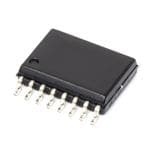
| 供应商器件封装 | 16-SOIC N |
| 信噪比 | 84 dB ADC/84 dB DAC |
| 信噪比,ADC/DAC(db)(典型值) | - |
| 其它名称 | 336-1382 |
| 分辨率 | 16 bit |
| 分辨率(位) | 16 b |
| 动态范围,ADC/DAC(db)(典型值) | 84 / 84 |
| 包装 | 管件 |
| 单位重量 | 189.320 mg |
| 商标 | Silicon Labs |
| 安装类型 | 表面贴装 |
| 安装风格 | SMD/SMT |
| 封装 | Tube |
| 封装/外壳 | 16-SOIC(0.154",3.90mm 宽) |
| 封装/箱体 | SOIC-16 |
| 工作温度 | 0°C ~ 70°C |
| 工厂包装数量 | 48 |
| 接口类型 | Serial |
| 数据接口 | 串行 |
| 最大工作温度 | + 70 C |
| 最小工作温度 | 0 C |
| 标准包装 | 48 |
| 电压-电源,数字 | 3 V ~ 5.25 V |
| 电压-电源,模拟 | 3 V ~ 5.25 V |
| 类型 | 声带 |
| 系列 | Si3000 |
| 转换速率 | 12 kHz |

.jpg)


- 商务部:美国ITC正式对集成电路等产品启动337调查
- 曝三星4nm工艺存在良率问题 高通将骁龙8 Gen1或转产台积电
- 太阳诱电将投资9.5亿元在常州建新厂生产MLCC 预计2023年完工
- 英特尔发布欧洲新工厂建设计划 深化IDM 2.0 战略
- 台积电先进制程称霸业界 有大客户加持明年业绩稳了
- 达到5530亿美元!SIA预计今年全球半导体销售额将创下新高
- 英特尔拟将自动驾驶子公司Mobileye上市 估值或超500亿美元
- 三星加码芯片和SET,合并消费电子和移动部门,撤换高东真等 CEO
- 三星电子宣布重大人事变动 还合并消费电子和移动部门
- 海关总署:前11个月进口集成电路产品价值2.52万亿元 增长14.8%


PDF Datasheet 数据手册内容提取
Si3000 VOICEBAND CODEC WITH MICROPHONE/SPEAKER DRIVE Features Complete voice codec solution includes the following: 84 dB ADC Dynamic Range Support for 32 Headphones 84 dB DAC Dynamic Range 3:1 Analog Input Mixer 4–12 kHz Sample Rates 3.3–5.0 V Power Supply 30 dB Microphone Pre-Amp Direct Serial Interface to DSPs Programmable Input Gain/ Direct Connection to Si303x/44/56, Ordering Information: Attenuation: –34.5 dB to 12 dB serial interface DAA chipsets Programmable Output Gain/ Low profile 16-Pin SOIC Package See page 29. Attenuation: –34.5 dB to 12 dB RoHS-compliant package available Pin Assignments Applications Si3000 Modem Voice Channel (DSVD) Speech Processing Telephony General Purpose Analog I/O SPKRR 1 16 SPKRL Companion chip for FDX MBIAS 2 15 LINEO ISOmodems with voice features HDST 3 14 GND SDI 4 13 V A Description SDO 5 12 V D FSYNC 6 11 LINEI The Si3000 is a complete voice band audio codec solution that offers high MCLK 7 10 MIC integration by incorporating programmable input and output gain/ SCLK 8 9 RESET attenuation, a microphone bias circuit, handset hybrid circuit, and an output drive for 32 headphones. The Si3000 can be connected directly to the Si3034, Si3035, Si3044, and Si3056 North American and international DAA chipsets through their daisy-chaining serial interface. It also serves as a companion chip to a FAT ISOmodem chipset with voice features, providing hardware support for a handset and speaker phone. The device operates from a single 3.3 to 5 V power supply and is available in a 16-pin small outline package (SOIC). Functional Block Diagram Si3000 MBIAS 0/+10/+20/+30 dB MSCCLLKK PArtotegn Guaationr/ Pass Filter ADC MIC FSYNC High 0/+10/+20 dB LINEI SDI InDteigrfiatacle Handset HDST SDO Hybrid 0/–6/–12/–18 dB SPKRR Prog Gain/ DAC Headphone Attenuator Driver SPKRL LINEO RESET 0/–6/–12/–18 dB Rev. 1.4 12/10 Copyright © 2010 by Silicon Laboratories Si3000
Si3000 2 Rev. 1.4
Si3000 TABLE OF CONTENTS Section Page 1. Electrical Specifications . . . . . . . . . . . . . . . . . . . . . . . . . . . . . . . . . . . . . . . . . . . . . . . . . . .4 2. Functional Description . . . . . . . . . . . . . . . . . . . . . . . . . . . . . . . . . . . . . . . . . . . . . . . . . . .14 2.1. Analog Inputs . . . . . . . . . . . . . . . . . . . . . . . . . . . . . . . . . . . . . . . . . . . . . . . . . . . . . .14 2.2. Pre-amp/Microphone Bias Circuit . . . . . . . . . . . . . . . . . . . . . . . . . . . . . . . . . . . . . . .14 2.3. Programmable Input Gain/Attenuation . . . . . . . . . . . . . . . . . . . . . . . . . . . . . . . . . . .14 2.4. Analog Outputs . . . . . . . . . . . . . . . . . . . . . . . . . . . . . . . . . . . . . . . . . . . . . . . . . . . . .14 2.5. Programmable Output Gain/Attenuation . . . . . . . . . . . . . . . . . . . . . . . . . . . . . . . . . .15 2.6. Line Output . . . . . . . . . . . . . . . . . . . . . . . . . . . . . . . . . . . . . . . . . . . . . . . . . . . . . . . .15 2.7. Speaker Output . . . . . . . . . . . . . . . . . . . . . . . . . . . . . . . . . . . . . . . . . . . . . . . . . . . . .15 2.8. Digital Interface . . . . . . . . . . . . . . . . . . . . . . . . . . . . . . . . . . . . . . . . . . . . . . . . . . . . .15 2.9. Clock Generation Subsystem . . . . . . . . . . . . . . . . . . . . . . . . . . . . . . . . . . . . . . . . . .17 2.10. Sleep Mode . . . . . . . . . . . . . . . . . . . . . . . . . . . . . . . . . . . . . . . . . . . . . . . . . . . . . . .18 2.11. Loopback Operation . . . . . . . . . . . . . . . . . . . . . . . . . . . . . . . . . . . . . . . . . . . . . . . .18 2.12. Reducing Power-on Pop Noise . . . . . . . . . . . . . . . . . . . . . . . . . . . . . . . . . . . . . . . .18 3. Control Registers . . . . . . . . . . . . . . . . . . . . . . . . . . . . . . . . . . . . . . . . . . . . . . . . . . . . . . . .19 4. Pin Descriptions: Si3000 . . . . . . . . . . . . . . . . . . . . . . . . . . . . . . . . . . . . . . . . . . . . . . . . . .27 5. Ordering Guide . . . . . . . . . . . . . . . . . . . . . . . . . . . . . . . . . . . . . . . . . . . . . . . . . . . . . . . . . .29 6. Package Outline: 16-Pin SOIC . . . . . . . . . . . . . . . . . . . . . . . . . . . . . . . . . . . . . . . . . . . . . .30 7. 16-Pin SOIC Land Pattern . . . . . . . . . . . . . . . . . . . . . . . . . . . . . . . . . . . . . . . . . . . . . . . . .31 8. Package Markings (Top Markings) . . . . . . . . . . . . . . . . . . . . . . . . . . . . . . . . . . . . . . . . . .32 8.1. Si3000-C-GS Top Marking . . . . . . . . . . . . . . . . . . . . . . . . . . . . . . . . . . . . . . . . . . . .32 8.2. Si3000-C-FS Top Marking . . . . . . . . . . . . . . . . . . . . . . . . . . . . . . . . . . . . . . . . . . . .32 Document Change List . . . . . . . . . . . . . . . . . . . . . . . . . . . . . . . . . . . . . . . . . . . . . . . . . . . . .33 Contact Information . . . . . . . . . . . . . . . . . . . . . . . . . . . . . . . . . . . . . . . . . . . . . . . . . . . . . . . .34 Rev. 1.4 3
Si3000 1. Electrical Specifications Table 1. Recommended Operating Conditions Parameter Symbol Test Condition Min1 Typ Max1 Unit Ambient Temperature T F and K-grade 0 25 70 °C A Si3000 Supply Voltage, Analog2 V 3.0 3.3/5.0 5.25 V A Si3000 Supply Voltage, Digital2,3 V 3.0 3.3/5.0 5.25 V D Notes: 1. All minimum and maximum specifications are guaranteed and apply across the recommended operating conditions. Typical values apply at nominal supply voltages and an operating temperature of 25°C unless otherwise stated. 2. The digital supply, VD, and analog supply, VA, can operate from either 3.3 V or 5.0 V. The Si3000 supports interface to 3.3 V logic when operating from 3.3 V. V must be within 0.6 V of V . D A 3. The Si3000 specifications are guaranteed using the typical application circuit (including component tolerance) of Figure 13. Table 2. DC Characteristics, V /V = 5 V A D (V = 5 V ±5%, V = 5 V ±5%, T = 0 to 70°C) A D A Parameter Symbol Test Condition Min Typ Max Unit High Level Input Voltage V 3.5 — — V IH Low Level Input Voltage V — — 0.8 V IL High Level Output Voltage V I = –2 mA 3.5 — — V OH O Low Level Output Voltage V I = 2 mA — — 0.4 V OL O Input Leakage Current I –10 — 10 µA L Power Supply Current, Analog1 I V pin — 6.5 10 mA A A Power Supply Current, Digital2 I V pin — 10 15 mA D D Total Supply Current, Sleep Mode3 — — 1.5 mA Notes: 1. No loads at DAC outputs, no load at MBIAS, Fs=12.5 kHz. 2. Slave mode operation, Fs = 12.5 kHz. 3. All inputs, except MCLK, are held static, and all outputs are unloaded. Table 3. DC Characteristics, V /V = 3.3 V A D (V = 3.3 V ±10%, V = 3.3 V ±10%, T = 0 to 70°C) A D A Parameter Symbol Test Condition Min Typ Max Unit High Level Input Voltage V 2.4 — — V IH Low Level Input Voltage V — — 0.8 V IL High Level Output Voltage V I = –2 mA 2.4 — — V OH O Low Level Output Voltage V I = 2 mA — — 0.35 V OL O Input Leakage Current I –10 — 10 µA L Power Supply Current, Analog I V pin — 6 10 mA A A Power Supply Current, Digital2 I V pin — 6 10 mA D D Total Supply Current, Sleep Mode3 — — 1.5 mA Notes: 1. No loads at DAC outputs, no load at MBIAS, Fs=12.5 kHz. 2. Slave mode operation, Fs = 12.5 kHz. 3. All inputs, except MCLK, are held static, and all outputs are unloaded. 4 Rev. 1.4
Si3000 Table 4. AC Characteristics (V , V = 5 V ±5% or 3.3 V ±10%, T = 0 to 70°C) A D A Parameter Symbol Test Condition Min Typ Max Unit ADC Resolution — 16 — Bits ADC Dynamic Range1,2 ADCDR VIN = 1 kHz, –3 dB 80 84 — dB ADC Total Harmonic Distortion3 ADCTHD VIN = 1 kHz, –3 dB, MIC/LINEI — –80 –62 dB V , V = 3.3 V ±10% VIN = 1 kHz, –3 dB, HDST — –80 –62 A D ADC Total Harmonic Distortion3 ADCTHD VIN = 1 kHz, –3 dB, MIC/LINEI — –80 –76 dB V , V = 5 V ±5% VIN = 1 kHz, –3 dB, HDST — –80 –71 A D ADC Full Scale Level (0 dB gain)4 V Vin = 1 kHz — 1 — V RX rms ADC Programmable Input Gain –34.5 — 12 dB ADC Input Gain Step Size — 1.5 — dB ADC Freq Response5 F Low –3 dB corner — 33 — Hz RR ADC Freq Response5 F 300 Hz –0.1 — 0 dB RR ADC Freq Response F 3400 Hz –0.2 — 0 dB RR Line In Preamp Gain — 0/10/20 — dB Mic In Preamp Gain — 0/10/20/ — dB 30 ADC Input Resistance 0 dB Preamp Gain — 20 — k ADC Input Capacitance — 15 — pF ADC Gain Drift A VIN = 1 kHz — 0.002 — dB/°C T DAC Resolution — 16 — Bits DAC Dynamic Range1,2 DACDR VIN = 1 kHz, –6 dB 80 84 — dB DAC Total Harmonic Distortion3 DACTHD VIN=1 kHz,–6 dB,LINEO,600 — –76 –60 dB V , V = 3.3 V ±10% VIN=1 kHz,–6 dB, SPKR, 60 — –72 –60 A D VIN=1 kHz,–6 dB, HDST, 600 — –80 –70 DAC Total Harmonic Distortion3 DACTHD VIN=1 kHz,–3 dB,LINEO,600 — –76 –65 dB V , V = 5 V ±5% VIN=1 kHz,–3 dB, SPKR, 60 — –72 –65 A D VIN=1 kHz,–3 dB, HDST, 600 — –80 –76 DAC Full Scale Level (0 dB gain) V — 1 — V RX rms DAC Programmable Output Gain –34.5 — 12 dB Notes: 1. DR = VIN + 20 log (RMS signal/RMS noise). Measurement bandwidth is 300 to 3400 Hz. Valid sample rate ranges between 4000 and 12000 Hz. 2. 0 dB setting for analog and digital attenuation/gain. 3. THD = 20 log (RMS distortion/RMS signal). Valid sample rate ranges between 4000 and 12000 Hz. 4. At 0 dB gain setting, 1 V input corresponds to –1.5 dB of full scale digital output code. rms 5. These characteristics are determined by external components. See Figure 13. 6. With a 600 load. Output starts clipping with half of full scale digital input, which corresponds to a 0.5 Vrms output. Rev. 1.4 5
Si3000 Table 4. AC Characteristics (Continued) (V , V = 5 V ±5% or 3.3 V ±10%, T = 0 to 70°C) A D A Parameter Symbol Test Condition Min Typ Max Unit DAC Output Gain Step Size — 1.5 — dB DAC Freq Response5 F Low –3 dB corner — 33 — Hz RR DAC Freq Response5 F 300 Hz –0.01 — 0 dB RR DAC Freq Response F 3400 Hz –0.2 — 0 dB RR DAC Line Output Load Resistance 600 — — DAC Line Output Load Capacitance — — 40 pF DAC SPKR Output Load Resistance — 60 — DAC Gain Drift A VIN = 1 kHz — 0.002 — dB/°C T Interchannel Isolation (Crosstalk) — 90 — dB HDST Full Scale Level Input — 0.5 — V rms HDST Full Scale Level Output6 — 1.0 — V rms HDST Output Resistance Rout DC — 600 — MIC Bias Voltage V — 2.5 — V mbias MIC Power Supply Rejection Ratio PSRR — 40 — dB Notes: 1. DR = VIN + 20 log (RMS signal/RMS noise). Measurement bandwidth is 300 to 3400 Hz. Valid sample rate ranges between 4000 and 12000 Hz. 2. 0 dB setting for analog and digital attenuation/gain. 3. THD = 20 log (RMS distortion/RMS signal). Valid sample rate ranges between 4000 and 12000 Hz. 4. At 0 dB gain setting, 1 V input corresponds to –1.5 dB of full scale digital output code. rms 5. These characteristics are determined by external components. See Figure 13. 6. With a 600 load. Output starts clipping with half of full scale digital input, which corresponds to a 0.5 V output. rms Table 5. Absolute Maximum Ratings Parameter Symbol Value Unit DC Supply Voltage V , V –0.5 to 6.0 V D A Input Current, Si3000 Digital Input Pins I ±10 mA IN Digital Input Voltage V –0.3 to (V + 0.3) V IND D Operating Temperature Range T –10 to 100 °C A Storage Temperature Range T –40 to 150 °C STG Note: Permanent device damage may occur if the above Absolute Maximum Ratings are exceeded. Functional operation should be restricted to the conditions as specified in the operational sections of this data sheet. Exposure to absolute maximum rating conditions for extended periods may affect device reliability. 6 Rev. 1.4
Si3000 Table 6. Switching Characteristics—General Inputs (V , V = 5 V ±5% or 3.3 V ±10%,T = 0 to 70°C, C = 20 pF) A D A L Parameter1 Symbol Test Condition Min Typ Max Unit Cycle Time, MCLK t 16.67 — — ns mc MCLK Duty Cycle t 40 50 60 % dty Rise Time, MCLK t — — 5 ns r Fall Time, MCLK t — — 5 ns f RESET Pulse Width2 t 250 — — ns rl Rise Time, RESET t — 1 — µs Rr Notes: 1. All timing (except Rise and Fall time) is referenced to the 50% level of the waveform. Input test levels are V = V – IH D 0.4 V, V = 0.4 V. Rise and Fall times are referenced to the 20% and 80% levels of the waveform. IL 2. The minimum RESET pulse width is the greater of 5 s or 10 MCLK cycle times. tr tmc tf VIH MCLK VIL tRr RESET trl Figure 1. General Inputs Timing Diagram Rev. 1.4 7
Si3000 Table 7. Switching Characteristics—Serial Interface (V , V = 5 V ±5% or 3.3 V ±10%, T = 0 to 70°C, C = 20 pF) A D A L Parameter Symbol Test Condition Min Typ Max Unit Cycle Time, SCLK t 354 1/256 Fs — ns c SCLK Duty Cycle t — 50 — % dty Delay Time, SCLK to FSYNC t — — 10 ns d1 Delay Time, SCLK to SDO Valid t — — 20 ns d2 Delay Time, SCLK to FSYNC t — — 10 ns d3 Setup Time, SDI, before SCLK t 25 — — ns su Hold Time, SDI, after SCLK t 20 — — ns h Setup Time, FSYNC (mode 2) before t 25 — — ns su MCLK Hold Time, FSYNC (mode 2) after t 20 — — ns h MCLK Note: All timing is referenced to the 50% level of the waveform. Input test levels are VIH = VD – 0.4 V, VIL = 0.4 V tc VOH SCLK VOL td1 td3 FSYNC (mode 0) td3 FSYNC (mode 1) FSYNC (mode 2) t d2 16 Bit High-Z D15 D14 ... D2 D1 DD00 High-Z SDO tsu th 16 Bit D15 D14 ... D2 D1 D0 SDI Figure 2. Serial Interface Timing Diagram 8 Rev. 1.4
Si3000 Table 8. Digital FIR Filter Characteristics—Transmit and Receive (V , V = 5 V ±5% or 3.3 V ±10%, Sample Rate = 8 kHz, T = 0 to 70°C) A D A Parameter Symbol Min Typ Max Unit Passband (3 dB, HPFD = 1) F(3 dB) 0 — 3.6 kHz Passband (3 dB, HPFD = 0) F(3 dB) 0.01 — 3.6 kHz Passband Ripple Peak-to-Peak –0.1 — 0.1 dB Stopband — 4.4 — kHz Stopband Attenuation –74 — — dB Group Delay tgd — 12/Fs — sec Note: Typical FIR filter characteristics for Fs = 8000 Hz are shown in Figures 3, 4, 5, and 6. Table 9. Digital IIR Filter Characteristics—Transmit and Receive (V , V = 5 V ±5% or 3.3 V ±10%, Sample Rate = 8 kHz, T = 70°C) A D A Parameter Symbol Min Typ Max Unit Passband (3 dB, HPFD = 1) F(3 dB) 0 — 3.6 kHz Passband (3 dB, HPFD = 0) F(3 dB) 0.01 — 3.6 kHz Passband Ripple Peak-to-Peak –0.2 — 0.2 dB Stopband — 4.4 — kHz Stopband Attenuation –40 — — dB Group Delay tgd — 1.6/Fs — sec Note: Typical IIR filter characteristics for Fs = 8000 Hz are shown in Figures 7, 8, 9, and 10. Figures 11 and 12 show group delay versus input frequency. Rev. 1.4 9
Si3000 B B d d n - n - o o ati ati u u n n e e Att Att Input Frequency - Hz Input Frequency - Hz Figure 3. FIR Receive Filter Response Figure 5. FIR Transmit Filter Response B B d d n - n - o o ati ati u u n n e e Att Att Input Frequency - Hz Input Frequency - Hz Figure 4. FIR Receive Filter Passband Ripple Figure 6. FIR Transmit Filter Passband Ripple For Figures 3–6, all filter plots apply to a sample rate of Fs = 8 kHz. The filters scale with the sample rate as follows: F = 0.4125 Fs (0.1 dB) F = 0.45 Fs (– 3 dB) where Fs is the sample frequency. 10 Rev. 1.4
Si3000 B B d d - - n n o o ati ati u u n n e e Att Att Input Frequency - Hz Input Frequency - Hz Figure 7. IIR Receive Filter Response Figure 10. IIR Transmit Filter Passband Ripple B d - n atio µs u - n y e a Att Del Input Frequency - Hz Input Frequency - Hz Figure 8. IIR Receive Filter Passband Ripple Figure 11. IIR Receive Group Delay B d - n o s Attenuati Delay - µ Input Frequency - Hz Input Frequency - Hz Figure 9. IIR Transmit Filter Response Figure 12. IIR Transmit Group Delay Rev. 1.4 11
Si3000 T E S E N O H PSTN TELEP t i u c r i C n o i t a c 2 i l p p A l a c i p y T 0 0 0 3 i S 102 3. 1 e 10 =2 = ur g i F 12 Rev. 1.4
Si3000 ‘ Table 10. Component Values—Typical Application Symbol Value C1,C3,C6,C8 0.1 µF, 16 V, ±20% C2,C4,C5,C7,C9,C10 10 µF, 16 V, ±20% D1 Motorola MMBD914L J1,J2 Phonejack Stereo JP1 4 Header K1 Relay DPDT L1,L2 Ferrite Bead R1 0 , 1/4 W ±5% R2 51 , 1/4 W ±5% R4 10 k, 1/4 W ±5% R8 2.2 k, 1/4 W, ±5% R9 10 , 1/16 W, ±5% R11,R12 30 , 1/16 W, ±5% U2 LM317LZ Q1 PNP Transistor Rev. 1.4 13
Si3000 2. Functional Description 2.2. Pre-amp/Microphone Bias Circuit An internal amplifier with a selectable gain of 0 dB, The Si3000 is a highly integrated voice bandwidth audio 10 dB, 20 dB, or 30 dB is provided for the MIC input and codec which contains a single 16-bit A/D converter and an internal amplifier with a selectable gain of 0 dB, D/A converter. The analog input path contains a 10 dB, or 20 dB, is provided for the LINEI input. AC microphone input with selectable gain, a line level input coupling is required for both inputs because any DC with selectable gain, and a handset input. Each of the offset on the input will be amplified if gain is selected. inputs go through a mixer prior to A/D conversion. The Gain settings for the LINEI and MIC inputs are achieved result of this A/D conversion is a 16-bit 2s complement by writing the RX Gain Control 1 register 5. When gain signed number. Following the A/D converter is a digital is disabled, these inputs become line level inputs with a programmable gain amplifier. The analog output path full-scale input of 1 Vrms. contains a digital programmable gain amplifier feeding a A microphone bias circuit is provided on-chip which single 16-bit D/A converter. The DAC output is provided consists of a 2.5 V reference output capable of sourcing to a line output, a headphone drive output, and a up to 5 mA of current. This circuit can be used for active handset output. Control for the various functions microphones requiring a bias source. available on the Si3000 as well as the audio data are communicated to the device over a serial interface. 2.3. Programmable Input Gain/Attenuation The Si3000 can be connected directly to the Si3035, The signals from the microphone, line, or handset inputs Si3034, Si3044, or Si3056 in modem applications are mixed and then routed to the A/D converter and a requiring a voice channel, or the device can be used as digital programmable gain circuit which provides up to a stand-alone codec in other voice band applications. 12 dB of gain or –34.5 dB of attenuation in 1.5 dB steps. The Si3000 offers high integration, and it needs only a Level changes only take effect on zero crossings to few low-cost, discrete components as shown in minimize audible artifacts. The requested level change Figure 13. is implemented if no zero crossing is found after 256 2.1. Analog Inputs frames. Write the ADC Volume Control register 6 to set digital input gain/attenuation. The typical connection diagram (Figure 13) shows the recommended external analog circuitry for the Si3000. 2.4. Analog Outputs The device supports three mono analog inputs—line The analog outputs of the D/A converter are routed to a level, microphone level, and a handset input. Each of line level output (LINEO), a pair of speaker outputs these inputs is provided to a mixer circuit prior to A/D (SPKRL and SPKRR), and a handset. Each analog conversion. Each analog input may also be muted by output can be independently muted. writing the appropriate bits in the control registers. Unused analog inputs should be tied to GND through a 0.1 F capacitor. This prevents any DC current flow. Si3034/35/44/56 Chipsets DAA DAA TIP System-Side Line-Side Discretes Device Device RING DSP SPKR Si3000 Handset Voice Codec Line Mic Figure 14. Si3000 with Silicon Labs DAA System Diagram 14 Rev. 1.4
Si3000 2.5. Programmable Output Gain/Attenuation frequency and the value of the sample rate control registers 3 and 4 determine the sample rate (Fs). The Prior to D/A conversion, the Si3000 contains a digital serial port clock, SCLK, runs at 256 bits per frame, programmable gain/attenuator which provides up to where the frame rate is equivalent to the sample rate. 12 dB of gain or –34.5 dB of attenuation in 1.5 dB steps. Digital information is transferred between the DSP and Level changes only take effect on zero crossings to the Si3000 in the form of 16-bit Primary Frames and 16- minimize audible artifacts. The requested level change bit Secondary Frames. There are separate pins for is implemented if no zero crossing is found after 256 receive (SDO) and transmit (SDI) functions, providing frames. Write the DAC Volume Control (register 7) to simultaneous receive/transmit operation within each set digital input gain/attenuation. frame. 2.6. Line Output Primary Frames are used for digital audio data samples. LINEO is a line level analog output signal centered Primary Frames occur at the frame rate and are always around a common mode voltage. The minimum present. recommended load impedance is 600 . This output is Secondary Frames are used for accessing internal a fully filtered output with a 1 Vrms full scale range. The Si3000 registers. Secondary Frames are not always only external component required is the 10 F DC present and are requested on-demand. When blocking capacitor shown in Figure 13 on page 12. This Secondary Frames are present, they occur mid-point output may be muted through the LOM bit in register 6 between Primary Frames. Hence, no Primary Frames or attenuated by setting the analog attenuation bits in are dropped. register 9. On Primary Frame transmits (DSP to Si3000), the 2.7. Speaker Output Si3000 treats the LSB (16th bit) as a flag to request a The SPKRL and SPKRR are mono, in-phase, analog Secondary Frame. Set the primary frame LSB = 1 to outputs capable of driving a small loudspeaker whose request a secondary frame; otherwise, set the primary impedance is typically 32 (see Figure 13 on page 12). frame LSB = 0. Therefore, out of 16-bits of transmit data The speaker outputs may be muted through the SLM on SDI, only 15-bits represent actual audio data. When and SRM bits in the DAC Gain Control register 7 or secondary frames are not present, no transmission attenuated by setting the analog attenuation bits in occurs during this time slot. register 9. On Primary Frames receives (Si3000 to DSP), the Si3000 drives SDO with 16-bits of audio data, if the 2.8. Digital Interface Si3000 is in either Serial Mode 0 or 1. However, if the The Si3000 has two serial interface modes that support Si3000 is in SLAVE mode (Mode 2), the Si3000 most standard modem DSPs. These modes are supplies 15-bits of Audio Data to the DSP and always selected by the addition of a 50 k pull-down/up resistor drives the LSB zero. This feature is designed to work on the SDO and SCLK pins as shown in Figure 13 on with the Si3021 register 14 SSEL set to 10. In this page 12. The key difference between these two serial system configuration, when the DSP receives Primary modes is the operation of the FSYNC signal. Table 11 Frames, it can check the LSB to determine whether the summarizes the serial mode definitions. receive data is from the Si3021 or from the Si3000. Table 11. Serial Modes On Secondary Frame receives and transmits; the Si3000 treats the input and output serial stream as 16- Mode SCLK* SDO* Description bits of data. Figure 15 shows the relative timing of the 0 0 0 FSYNC frames data serial frames. 1 0 1 FSYNC pulse starts data frame Figure 16 and Figure 17 illustrate the secondary frame write cycle and read cycle, respectively. During a read 2 1 0 Slave mode cycle, the R/W bit is high and the 5-bit address field 3 1 1 Reserved contains the address of the register to be read. The *Note: Pull-up/pull-down states contents of the 8-bit control register are placed on the SDO signal. During a write cycle, the R/W bit is low and the 5-bit address field contains the address of the The digital interface consists of a single synchronous register to be written. The 8-bit data to be written serial link which communicates audio and control data. immediately follows the address on SDI. Only one In slave mode, SCLK is connected only to the pullup/ register can be read or written during each secondary pulldown resistor, and MCLK is a 256 Fs input which is frame. See "3. Control Registers" on page 19 for the internally multiplied using the on-chip phase-locked loop register addresses and functions. (PLL) to clock the A/D converter and D/A converter. In master mode, the master clock (MCLK) is an input and the serial data clock (SCLK) is an output. The MCLK Rev. 1.4 15
Si3000 FSYNC Primary Secondary Primary D15 – D1 D0 = 0 (Software FC Bit) SDI XMT Data Secondary XMT Data Update SDO RCV Data SeUcpodnadtaery RCV Data 16 SCLKs 128 SCLKs 256 SCLKs Figure 15. Secondary Request FSYNC (mode 0) FSYNC (mode 1) D15 D14 D13 D12 D11 D10 D9 D8 D7 D6 D5 D4 D3 D2 D1 D0 SDI 0 0 0 A A A A A D D D D D D D D R/W SDO Figure 16. Secondary Communication Data Format—Write Cycle FSYNC (mode 0) FSYNC (mode 1) D15 D14 D13 D12 D11 D10 D9 D8 D7 D0 SDI 0 0 1 A A A A A R/W D7 D6 D5 D4 D3 D2 D1 D0 SDO High Z D D D D D D D D High Z Figure 17. Secondary Frame Format—Read Cycle 16 Rev. 1.4
Si3000 FUP1 FPLL1 MCLK ÷ N1 P ÷ 5 or VCO1 1024·Fs ÷ 10* D *Note: See PLL bit in Register 2. ÷ M1 8 bits Figure 18. Clock Generation Subsystem (PLL) 2.9. Clock Generation Subsystem Table 12. MCLK Examples for 8 kHz The Si3000 contains an on-chip clock generator. Using a single MCLK input frequency, the Si3000 can MCLK (MHz) N1 M1 generate all the desired standard modem sample rates, 1.8432 9 200 as well as the common 11.025 kHz rate for audio 4.0000 25 256 playback. 4.0960 1 10 The clock generator consists of a phase-locked loop (PLL1) that achieves the desired sample frequency. 5.2800 33 256 Figure 18 illustrates the clock generator. The 5.7600 9 64 architecture of the PLL allows for fast lock time on initial 6.1440 3 20 start-up, fast lock time when changing modem sample rates and high noise immunity. A large number of MCLK 8.1920 1 5 frequencies between 1 MHz and 60 MHz are supported. 9.2160 9 40 2.9.1. Programming the Clock Generator 10.0800 63 256 As noted in Figure 18, the clock generator must output a 10.5600 33 128 clock equal to 1024*Fs, where Fs is the desired sample rate. The 1024*Fs clock is determined through 11.0592 27 100 programming of the following registers: 12.288 3 10 Register 3 - N1 divider, 8 bits. 14.7456 9 25 Register 4 - M1 divider, 8 bits 16.0000 25 64 N1 (register 3) and M1 (register 4) are 8-bit unsigned 18.4320 9 20 values. F is the clock provided to the MCLK pin. MCLK Table 12 lists several standard crystal rates that could 24.5760 3 5 be supplied to MCLK. 25.8048 63 100 When programming the registers of the clock generator, 33.7600 211 256 the order of register writes is important. For PLL updates, N1 (register 3) must always be written first, 44.2368 27 25 immediately followed by a write to M1 (register 4). 46.0800 9 8 Note: The values shown in Table 12 satisfy the equations 47.9232 117 100 above. However, when programming the registers for 48.0000 75 64 N1 and M1, the value placed in these registers must be one less than the value calculated from the equations. 56.0000 175 128 59.200 185 128 Rev. 1.4 17
Si3000 2.9.2. PLL Lock Times 3. Restore MCLK before initiating the power up sequence. The Si3000 changes sample rates very quickly. 4. Reset the Si3000 using the RESET pin (after MCLK is However, lock time will vary based on the programming present). of the clock generator. The following relationship 5. Program the registers to desired settings. describes the boundaries on PLL locking time: 2.11. Loopback Operation PLL lock time < 1 ms The Si3000 advanced design provides the It is recommended that the PLL be programmed during manufacturer with increased ability to determine system initialization. functionality during production line tests, as well as The final design consideration for the clock generator is support for end-user diagnostics. Two loopback modes the update rate of PLL. The following criteria must be exist for this purpose, allowing increased coverage of satisfied in order for the PLL to remain stable: system components. F =F N1144kHz UP1 MCLK The digital loopback1 mode allows an external device to send audio data to the SDI input pin and receive the Where F is shown in Figure 18. UP1 signal through the SDO output pin. In this mode, the 2.9.3. Setting Generic Sample Rates group delay of the digital filters is present. This mode The above clock generation description focuses on allows testing of the digital filters, DAC, and ADC. To common modem sample rates. The restrictions and enable this mode, set the DL1 bit of register 2, and clear equations above still apply; however, a more generic DL2. relationship between MCLK and Fs (the desired sample The digital loopback2 mode allows an external device to rate) is needed. The following equation describes this send audio data to the SDI input pin and receive the relationship: signal through the SDO output pin. This mode allows M1 51024Fs testing of the digital filters, but not the ADC and DAC. To -------- = -------------------------------- N1 MCLK enable this mode, set the DL2 bit of register 2, and clear DL1. where Fs is the sample frequency, and all other symbols are shown in Figure 18. 2.12. Reducing Power-on Pop Noise Knowing the MCLK frequency and desired sample rate To minimize power-on pop during initialization, a waiting the values for the M1 and N1 registers can be period is recommended before powering up the analog determined. When determining these values, remember output drivers. The waiting period starts when the reset to consider the range for each register as well as the signal to the Si3000 is negated. The wait time required minimum update rate for the first PLL. is dependent on the external load. Typically, the load The values determined for M1 and N1 must be adjusted consists of an AC coupling capacitor in series with an by minus one when determining the value written to the equivalent load resistor to ground. The equivalent load respective registers. This is due to internal logic, which resistor can either be a speaker load, or the input adds one to the value stored in the register. This resistance of an external amplifier. The rule-of-thumb for addition allows the user to write a zero value in any of the waiting period in msec is derived by C*(12+R). For the registers and the effective divide-by is one. A example, in the case of a 10 F AC coupling capacitor special case occurs when both M1 and N1 are and resistive load of 1.0 k the recommended waiting programmed with a zero value. When M1 and N1 are period is 10*(12+1) = 130 msec. both zero, the PLL is bypassed. If the analog outputs drive external amplifiers, another 2.10. Sleep Mode factor to consider is the voltage division ratio determined by R/(R+12), where R represents the input The Si3000 supports a low-power sleep mode. Sleep resistance of the external amplifier. This ratio must be mode is activated by setting the Chip Power Down kept as small as possible. A good target value is R = 1 (CPD) bit in register 1. When the Si3000 is in sleep k. If needed, add a load resistor in parallel with the mode, the MCLK signal may be stopped or remain amplifier input to lower the effective input resistance of active, but it must be active before waking up the the amplifier stage. Si3000. To take the Si3000 out of sleep mode, pulse the reset pin (RESET) low. In summary, the power down/up sequence is as follows: 1. Set the Power Down bit (PDN, register 6, bit 3). 2. MCLK may stay active or stop. 18 Rev. 1.4
Si3000 3. Control Registers Note: Any register not listed here is reserved and should not be written. Any register bit labelled reserved should be written to zero during writes to the register. Register 0 can be read (always returns 0) and written safely. Table 13. Register Summary Register Name Bit 7 Bit 6 Bit 5 Bit 4 Bit 3 Bit 2 Bit 1 Bit 0 1 Control 1 SR SPD LPD HPD MPD CPD 2 Control 2 HPFD PLL DL1 DL2 3 PLL1 Divide N1 Divider N1 4 PLL1 Multiply M1 Multiplier M1 5 RX Gain Control 1 LIG LIM MCG MCM HIM IIR 6 ADC Volume Control RXG LOM HOM 7 DAC Volume Control TXG SLM SRM 8 Status Report SLSC SRSC LOSC 9 Analog Attenuation LOT SOT Rev. 1.4 19
Si3000 Register 1. Control 1 Bit D7 D6 D5 D4 D3 D2 D1 D0 Name SR SPD LPD HPD MPD CPD Type R/W R/W R/W R/W R/W R/W Reset settings = 0000_0000 Bit Name Function 7 SR Software Reset. 1 = Sets all registers to their reset value. 0 = Enables chip for normal operation. Note: Bit will automatically clear after being set. 6:5 Reserved Read returns zero. 4 SPD Speaker Drive Power Down. 1= Normal operation 0 = Power down left and right speaker drive. 3 LPD Line Drive Power Down. 1 = Normal operation 0 = Power down line driver. 2 HPD Handset Drive Power Down. 1 = Normal operation 0 = Power down handset driver. 1 MPD MIC Bias Power Down. 1 = Power down MIC bias buffer. 0 = Normal operation 0 CPD Chip Power Down. 1 = Puts Si3000 into power down mode. 0 = Normal operation 20 Rev. 1.4
Si3000 Register 2. Control 2 Bit D7 D6 D5 D4 D3 D2 D1 D0 Name HPFD PLL DL1 DL2 Type R/W R/W R/W R/W Reset Settings = 0000_0000 Bit Name Function 7:5 Reserved Read returns zero. 4 HPFD High Pass Filter (HPF) Disable. 1 = HPF disabled 0 = HPF enabled 3 PLL PLL Divide by 10. 1 = Sets final stage of PLL to divide by 10. 0 = Sets final stage of PLL to divide by 5. 2 DL1 Digital Loopback. 1 = Enables digital loopback (DAC analog out ADC analog in). 0 = Normal operation 1 DL2 Digital Loopback. 1 = Enables digital loopback (DAC one bit ADC one bit). 0 = Normal operation 0 Reserved Read returns zero. Rev. 1.4 21
Si3000 Register 3. PLL1 Divide N1 Bit D7 D6 D5 D4 D3 D2 D1 D0 Name Divider N1 Type R/W Reset settings = 0000_0000 Bit Name Function 7:0 N1 N1. Contains the (value – 1) for determining the output frequency on PLL. Register 4. PLL1 Multiply M1 Bit D7 D6 D5 D4 D3 D2 D1 D0 Name Multiplier M1 Type R/W Reset settings = 0000_0000 Bit Name Function 7:0 M1 M1. Contains the (value – 1) for determining the output frequency on PLL. 22 Rev. 1.4
Si3000 Register 5. RX Gain Control 1 Bit D7 D6 D5 D4 D3 D2 D1 D0 Name LIG LIM MCG MCM HIM IIR Type R/W R/W R/W R/W R/W R/W Reset settings = 0100_0111 Bit Name Function 7:6 LIG Line in Gain. 11 = 20 dB gain 10 = 10 dB gain 01 = 0 dB gain 00 = Reserved 5 LIM Line in Mute. 1 = Line input muted 0 = Line input goes to mixer 4:3 MCG MIC Input Gain. 11 = 30 dB gain 10 = 20 dB gain 01 = 10 dB gain 00 = 0 dB gain 2 MCM MIC Input Mute. 1 = Mute MIC input 0 = MIC input goes into mixer. 1 HIM Handset Input Mute. 1 = Mute handset input 0 = Handset input goes into mixer. 0 IIR IIR Enable. 1 = Enables IIR filter 0 = Enables FIR filter Rev. 1.4 23
Si3000 Register 6. ADC Volume Control Bit D7 D6 D5 D4 D3 D2 D1 D0 Name RXG LOM HOM Type R/W R/W R/W Reset settings = 0101_1100 Bit Name Function 7 Reserved Read returns zero. 6:2 RXG RX PGA Gain Control. 11111 = 12 dB 10111 = 0 dB 00000 = –34.5 dB LSB = 1.5 dB 1 LOM Line Out Mute. 0 = Mute 1 = Active 0 HOM Handset Out Mute. 0 = Mute 1 = Active 24 Rev. 1.4
Si3000 Register 7. DAC Volume Control Bit D7 D6 D5 D4 D3 D2 D1 D0 Name TXG SLM SRM Type R/W R/W R/W Reset settings = 0101_1100 Bit Name Function 7 Reserved Read returns zero. 6:2 TXG TX PGA Gain Control. 11111 = 12 dB 10111 = 0 dB 00000 = –34.5 dB LSB = 1.5 dB 1 SLM SPKR_L Mute. 0 = Mute 1 = Active 0 SRM SPKR_R Mute. 0 = Mute 1 = Active Rev. 1.4 25
Si3000 Register 8. Status Report Bit D7 D6 D5 D4 D3 D2 D1 D0 Name SLSC SRSC LOSC Type R R R Reset settings = 0000_0000 Bit Name Function 7 SLSC SPK_L Short Circuit. 1 = Indicate short circuit status is detected at left speaker. 0 = Normal mode 6 SRSC SPK_R Short Circuit. 1 = Indicate short circuit status is detected at right speaker. 0 = Normal mode 5 LOSC Line Out Short Circuit. 1 = Indicate short circuit status is detected at line out. 0 = Normal mode 4:0 Reserved Read returns zero. Register 9. Analog Attenuation Bit D7 D6 D5 D4 D3 D2 D1 D0 Name LOT SOT Type R/W R/W Reset settings = 0000_0000 Bit Name Type 7:4 Reserved Read returns zero. 3:2 LOT Line Out Attenuation. 11 = –18 dB analog attenuation on Line Output. 10 = –12 dB analog attenuation on Line Output. 01 = –6 dB analog attenuation on Line Output. 00 = 0 dB analog attenuation on Line Output. 2:0 SOT Speaker Out Attenuation. 11 = –18 dB analog attenuation on Speaker Output. 10 = –12 dB analog attenuation on Speaker Output. 01 = –6 dB analog attenuation on Speaker Output. 00 = 0 dB analog attenuation on Speaker Output. 26 Rev. 1.4
Si3000 4. Pin Descriptions: Si3000 SPKRR 1 16 SPKRL MBIAS 2 15 LINEO HDST 3 14 GND SDI 4 13 V A SDO 5 12 V D FSYNC 6 11 LINEI MCLK 7 10 MIC SCLK 8 9 RESET Pin # Pin Name Description 1 SPKRR Speaker Right Output. Analog output capable of driving a 60 load. 2 MBIAS Microphone bias output. 3 HDST Handset Input/Output. Handset analog input/output. 4 SDI Serial Port Data In. Serial communication and control data that is generated by the System DSP to the Si3000. 5 SDO Serial Port Data Out. Serial communication data that is provided by the Si3000 to the system DSP. 6 FSYNC Frame Sync Output. Data framing signal that is used to indicate the start and stop of a communication data frame. 7 MCLK Master Clock Input. High speed master clock input. Generally supplied by the system crystal clock or DSP. 8 SCLK Serial Port Bit Clock Input/Output. Controls the serial data on SDO and latches the data on SDI. This pin is an input in slave mode and an output in master mode. 9 RESET Reset. An active low input that is used to reset all control registers to a defined initialized state. Also used to bring the Si3000 out of sleep mode. 10 MIC MIC Input. Microphone level or line level input. This input contains selectable gain of 0, 10, 20, or 30 dB with a full scale input level of 1 V . RMS 11 LINEI Line Input. Line level input with selectable gain of 0, 10, or 20 dB. The full scale input level is 1 V . RMS 12 V Digital Supply Voltage. D Provides the digital supply voltage to the Si3000. Nominally either 5 or 3.3 V and within 0.6 V of V . A Rev. 1.4 27
Si3000 Pin # Pin Name Description 13 V Analog Supply Voltage. A Provides the analog supply voltage to the Si3000. Nominally either 5 or 3.3 V and within 0.6 V of V . D 14 GND Ground. Connects to the system digital ground. 15 LINEO Line Output. Line level analog output with a 1 V full scale output level. RMS 16 SPKRL Speaker Left Output. Analog output capable of driving a 60 load. 28 Rev. 1.4
Si3000 5. Ordering Guide Table 14. Ordering Guide Part Number Package Lead-Free Temp. Range Si3000-C-FS SOIC-16 Yes 0 to 70 °C Si3000-C-GS SOIC-16 Yes –40 to 85 °C *Note: Add an “R” at the end of the device to denote tape and reel option. Rev. 1.4 29
Si3000 6. Package Outline: 16-Pin SOIC Figure 19 illustrates the package details for the Si3000. Table 15 lists the values for the dimensions shown in the illustration. Figure 19. 16-Pin Small Outline Integrated Circuit (SOIC) Package Table 15. Package Diagram Dimensions Dimension Min Max Dimension Min Max A — 1.75 L 0.40 1.27 A1 0.10 0.25 L2 0.25 BSC A2 1.25 — h 0.25 0.50 b 0.31 0.51 θ 0° 8° c 0.17 0.25 aaa 0.10 D 9.90 BSC bbb 0.20 E 6.00 BSC ccc 0.10 E1 3.90 BSC ddd 0.25 e 1.27 BSC Notes: 1. All dimensions shown are in millimeters (mm) unless otherwise noted. 2. Dimensioning and Tolerancing per ANSI Y14.5M-1994. 3. This drawing conforms to the JEDEC Solid State Outline MS-012, Variation AC. 4. Recommended card reflow profile is per the JEDEC/IPC J-STD-020C specification for Small Body Components. 30 Rev. 1.4
Si3000 7. 16-Pin SOIC Land Pattern Figure illustrates the recommended land pattern for the Si3000 16-pin SOIC. Table 16 lists the values for the dimensions shown in the illustration. Figure 20. 16-Pin SOIC Land Pattern Diagram Table 16. 16-Pin MSOP Land Pattern Dimensions Dimension Feature mm C1 Pad Column Spacing 5.40 E Pad Row Pitch 1.27 X1 Pad Width 0.60 Y1 Pad Length 1.55 Notes: General 1. All dimensions shown are in millimeters (mm) unless otherwise noted. 2. Dimensioning and Tolerancing per ASME Y14.5M-1994. 3. This Land Pattern Design is based on the IPC-7351 guidelines. 4. All dimensions shown are at Maximum Material Condition (MMC). Least Material Condition (LMC) is calculated based on a Fabrication Allowance of 0.05 mm. Solder Mask Design 5. All metal pads are to be non-solder mask defined (NSMD). Clearance between the solder mask and the metal pad is to be 60 µm minimum, all the way around the pad. Stencil Design 6. A stainless steel, laser-cut and electro-polished stencil with trapezoidal walls should be used to assure good solder paste release. 7. The stencil thickness should be 0.125 mm (5 mils). 8. The ratio of stencil aperture to land pad size should be 1:1. Card Assembly 9. A No-Clean, Type-3 solder paste is recommended. 10. The recommended card reflow profile is per the JEDEC/IPC J-STD-020 specification for Small Body Components. Rev. 1.4 31
Si3000 8. Package Markings (Top Markings) Codes for the Si3000-C-GS and Si3000-C-FS top marks are as follows: YY = Current Year WW = Work Week R = Die Revision TTTTT = Trace Code 8.1. Si3000-C-GS Top Marking 8.2. Si3000-C-FS Top Marking 32 Rev. 1.4
Si3000 DOCUMENT CHANGE LIST Revision 1.0 to Revision 1.1 Updated Functional Block Diagram. Removed all B-grade references. Updated Table 4 (AC Characteristics). Updated Figure 14. Removed analog loopback feature description. Revision 1.1 to Revision 1.2 Updated " Features" on page 1 and "5. Ordering Guide" on page 29 to add updated support for lead- free, RoHS-compliant packages. Updated document for compatibility with Silicon Laboratories 3rd generation serial interface DAA, the Si3056. Updated Figure 13 on page 12. Updated MIC and MICBIAS pin number labels. Changed standardized minimum input/output attenuation level to –34.5 dB. In some instances, this level was incorrectly specified at –36 dB. Updated SOIC package outline drawing and dimensions table. Revision 1.2 to Revision 1.3 Updated Table 6 on page 7. Updated Figure 1 on page 7. Updated Figure 2 on page 8. Updated Figure 13 on page 12. Updated "2.8. Digital Interface" on page 15. Updated "2.11. Loopback Operation" on page 18. Updated "4. Pin Descriptions: Si3000" on page 27. Revision 1.3 to Revision 1.4 Added extended temperature Si3000-C-GS to Table 14 ordering guide. Added Section 7, 16-Pin SOIC Land Pattern. Added Section 8, Package Top Markings. Rev. 1.4 33
Smart. Connected. Energy-Friendly Products Quality Support and Community www.silabs.com/products www.silabs.com/quality community.silabs.com Disclaimer Silicon Laboratories intends to provide customers with the latest, accurate, and in-depth documentation of all peripherals and modules available for system and software implementers using or intending to use the Silicon Laboratories products. Characterization data, available modules and peripherals, memory sizes and memory addresses refer to each specific device, and "Typical" parameters provided can and do vary in different applications. Application examples described herein are for illustrative purposes only. Silicon Laboratories reserves the right to make changes without further notice and limitation to product information, specifications, and descriptions herein, and does not give warranties as to the accuracy or completeness of the included information. Silicon Laboratories shall have no liability for the consequences of use of the information supplied herein. This document does not imply or express copyright licenses granted hereunder to design or fabricate any integrated circuits. The products must not be used within any Life Support System without the specific written consent of Silicon Laboratories. A "Life Support System" is any product or system intended to support or sustain life and/or health, which, if it fails, can be reasonably expected to result in significant personal injury or death. Silicon Laboratories products are generally not intended for military applications. Silicon Laboratories products shall under no circumstances be used in weapons of mass destruction including (but not limited to) nuclear, biological or chemical weapons, or missiles capable of delivering such weapons. Trademark Information Silicon Laboratories Inc., Silicon Laboratories, Silicon Labs, SiLabs and the Silicon Labs logo, CMEMS®, EFM, EFM32, EFR, Energy Micro, Energy Micro logo and combinations thereof, "the world’s most energy friendly microcontrollers", Ember®, EZLink®, EZMac®, EZRadio®, EZRadioPRO®, DSPLL®, ISOmodem ®, Precision32®, ProSLIC®, SiPHY®, USBXpress® and others are trademarks or registered trademarks of Silicon Laboratories Inc. ARM, CORTEX, Cortex-M3 and THUMB are trademarks or registered trademarks of ARM Holdings. Keil is a registered trademark of ARM Limited. All other products or brand names mentioned herein are trademarks of their respective holders. Silicon Laboratories Inc. 400 West Cesar Chavez Austin, TX 78701 USA http://www.silabs.com