ICGOO在线商城 > 射频/IF 和 RFID > RF 收发器 IC > SX1212IWLTRT
 Datasheet下载
- 型号: SX1212IWLTRT
- 制造商: SEMTECH
- 库位|库存: xxxx|xxxx
- 要求:
| 数量阶梯 | 香港交货 | 国内含税 |
| +xxxx | $xxxx | ¥xxxx |
查看当月历史价格
查看今年历史价格
SX1212IWLTRT产品简介:
ICGOO电子元器件商城为您提供SX1212IWLTRT由SEMTECH设计生产,在icgoo商城现货销售,并且可以通过原厂、代理商等渠道进行代购。 SX1212IWLTRT价格参考。SEMTECHSX1212IWLTRT封装/规格:RF 收发器 IC, IC 射频 仅限 TxRx 通用 ISM < 1GHz 300MHz ~ 510MHz 32-WFQFN 裸露焊盘。您可以下载SX1212IWLTRT参考资料、Datasheet数据手册功能说明书,资料中有SX1212IWLTRT 详细功能的应用电路图电压和使用方法及教程。
Semtech Corporation的SX1212IWLTRT是一款RF(射频)收发器IC,适用于多种无线通信应用场景。该芯片工作在431-510 MHz和862-930 MHz频段,支持LoRa调制技术,具有远距离、低功耗和高抗干扰能力的特点。

 应用场景

1. 物联网(IoT)
   - 智能城市:用于环境监测、智能路灯控制、垃圾管理等,通过低功耗广域网(LPWAN)实现远程数据传输。
   - 智能家居:可用于智能门锁、温湿度传感器、烟雾报警器等设备,提供可靠的无线通信连接。
   - 工业物联网(IIoT):适用于工厂自动化、设备监控、资产追踪等领域,帮助提高生产效率和维护管理。

2. 农业与环境监测
   - 精准农业:部署在田间地头,用于土壤湿度、温度、光照等参数的监测,帮助农民优化灌溉和施肥。
   - 气象站:用于天气预报、灾害预警等,通过无线网络实时传输气象数据。

3. 物流与资产管理
   - 货物追踪:安装在运输车辆或货物上,实现实时位置跟踪和状态监控,确保物流安全和高效。
   - 资产追踪:用于仓库、医院、学校等场所,对贵重设备或物品进行定位和管理。

4. 智能表计
   - 水电气表:集成到智能水表、电表、燃气表中,实现远程抄表和自动计费,减少人工成本并提高准确性。

5. 应急通信
   - 灾难救援:在地震、洪水等自然灾害发生时,利用其远距离和低功耗特性,建立临时通信网络,保障救援工作的顺利进行。

6. 安防系统
   - 无线报警器:用于家庭、商业场所的安全防护,通过无线方式将警报信息发送到监控中心或用户手机。

7. 医疗健康
   - 可穿戴设备:如智能手环、心率监测仪等,通过无线通信将健康数据上传至云端,供医生或用户分析。

总之,SX1212IWLTRT凭借其卓越的性能和灵活性,广泛应用于各种需要低功耗、远距离无线通信的领域,为现代科技生活提供了可靠的技术支持。
| 参数 | 数值 |
| 产品目录 | |
| 描述 | IC TXRX 300MHZ-510MHZ 32-TQFN |
| 产品分类 | RF 收发器 |
| 品牌 | Semtech |
| 数据手册 | |
| 产品图片 |
|
| 产品型号 | SX1212IWLTRT |
| PCN设计/规格 | |
| rohs | 无铅 / 符合限制有害物质指令(RoHS)规范要求 |
| 产品系列 | - |
| 产品目录页面 | |
| 其它名称 | SX1212IWLCT |
| 功率-输出 | 12.5dBm |
| 包装 | 剪切带 (CT) |
| 天线连接器 | PCB,表面贴装 |
| 存储容量 | - |
| 封装/外壳 | 32-TQFN |
| 工作温度 | -40°C ~ 85°C |
| 应用 | AMR,ISM,家庭自动化,程序控制 |
| 数据接口 | PCB,表面贴装 |
| 数据速率(最大值) | 150kbps |
| 标准包装 | 1 |
| 灵敏度 | -110dBm |
| 电压-电源 | 2.1 V ~ 3.6 V |
| 电流-传输 | 25mA |
| 电流-接收 | 3mA |
| 调制或协议 | FSK,OOK |
| 频率 | 300MHz ~ 510MHz |


- 商务部:美国ITC正式对集成电路等产品启动337调查
- 曝三星4nm工艺存在良率问题 高通将骁龙8 Gen1或转产台积电
- 太阳诱电将投资9.5亿元在常州建新厂生产MLCC 预计2023年完工
- 英特尔发布欧洲新工厂建设计划 深化IDM 2.0 战略
- 台积电先进制程称霸业界 有大客户加持明年业绩稳了
- 达到5530亿美元!SIA预计今年全球半导体销售额将创下新高
- 英特尔拟将自动驾驶子公司Mobileye上市 估值或超500亿美元
- 三星加码芯片和SET,合并消费电子和移动部门,撤换高东真等 CEO
- 三星电子宣布重大人事变动 还合并消费电子和移动部门
- 海关总署:前11个月进口集成电路产品价值2.52万亿元 增长14.8%


PDF Datasheet 数据手册内容提取
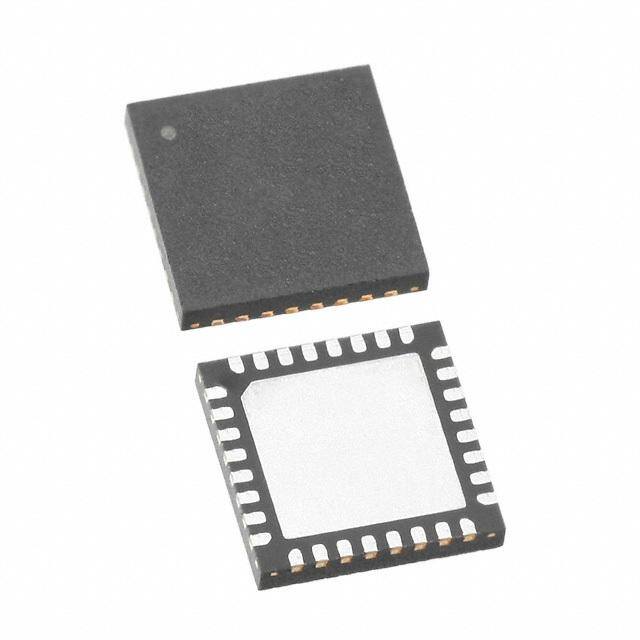
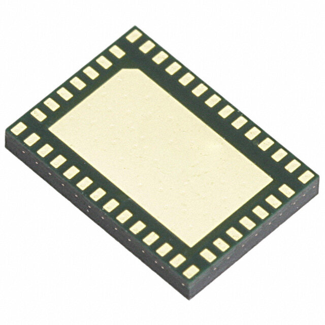
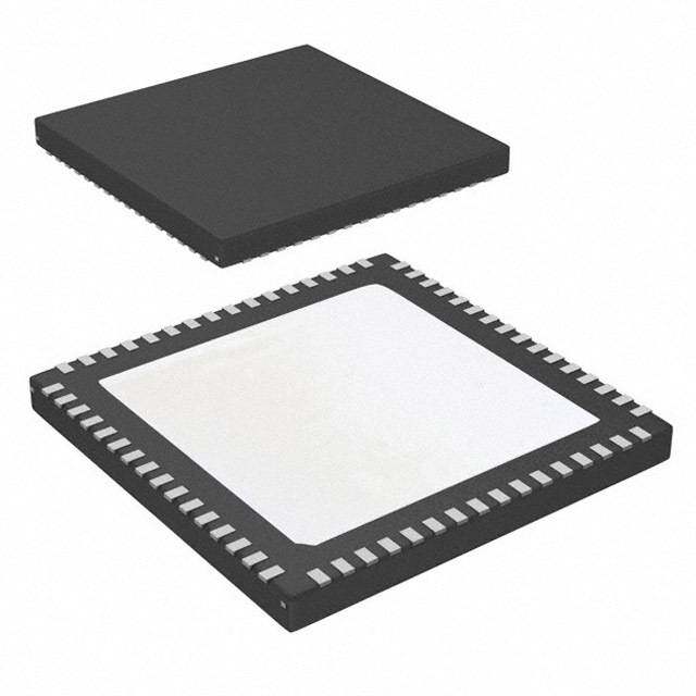
SX1212 Transceiver Ultra-Low Power Integrated 300-510MHz Transceiver ADVANCED COMMUNICATIONS & SENSING General Description Features The SX1212 is a low cost single-chip transceiver (cid:131) Low Rx power consumption: 3mA operating in the frequency ranges from 300MHz to (cid:131) Low Tx power consumption: 25 mA @ +10 dBm 510MHz. The SX1212 is optimized for very low power (cid:131) Good reception sensitivity: down to -104 dBm at consumption (3mA in receiver mode). It incorporates a 25 kb/s in FSK, -110 dBm at 2kb/s in OOK baseband modem with data rates up to 150 kb/s. Data (cid:131) Programmable RF output power: up to +12.5 dBm handling features include a sixty-four byte FIFO, in 8 steps packet handling, automatic CRC generation and data (cid:131) Packet handling feature with data whitening and whitening. Its highly integrated architecture allows for automatic CRC generation minimum external component count whilst maintaining (cid:131) RSSI (Received Signal Strength Indicator) design flexibility. All major RF communication (cid:131) Bit rates up to 150 kb/s, NRZ coding parameters are programmable and most of them may (cid:131) On-chip frequency synthesizer be dynamically set. It complies with European (ETSI (cid:131) FSK and OOK modulation EN 300-220 V2.1.1) and North American (FCC part (cid:131) Incoming sync word recognition 15.247 and 15.249) regulatory standards. (cid:131) Built-in Bit-Synchronizer for incoming data and clock synchronization and recovery Ordering Information (cid:131) 5 x 5 mm TQFN package (cid:131) Optimized Circuit Configuration for Low-cost applications Table 1: Ordering Information Applications Minimum Order Part number Delivery Quantity / Multiple SX1212IWLTRT Tape & Reel 3000 pieces (cid:131) Wireless alarm and security systems (cid:131) Wireless sensor networks (cid:131) Automated Meter Reading (cid:131) TQFN-32 package – Operating range [-40;+85°C] (cid:131) Home and building automation (cid:131) T refers to Lead Free packaging (cid:131) Industrial monitoring and control (cid:131) This device is WEEE and RoHS compliant (cid:131) Remote Wireless Control (cid:131) Active RFID PHY Application Circuit Schematic Rev 2 – June 18th, 2009 Page 1 of 77 www.semtech.com
SX1212 ADVANCED COMMUNICATIONS & SENSING Table of Contents 1. General Description...................................................................5 5.2.5. Control......................................................................40 1.1. Simplified Block Diagram...................................................5 5.3. Continuous Mode.............................................................41 1.2. Pin Diagram.......................................................................6 5.3.1. General Description.................................................41 1.3. Pin Description...................................................................7 5.3.2. Tx Processing..........................................................41 2. Electrical Characteristics............................................................8 5.3.3. Rx Processing..........................................................42 2.1. ESD Notice........................................................................8 5.3.4. Interrupt Signals Mapping........................................42 2.2. Absolute Maximum Ratings...............................................8 5.3.5. uC Connections........................................................43 2.3. Operating Range...............................................................8 5.3.6. Continuous Mode Example......................................43 2.4. Chip Specification..............................................................8 5.4. Buffered Mode..................................................................44 2.4.1. Power Consumption..................................................8 5.4.1. General Description.................................................44 2.4.2. Frequency Synthesis.................................................9 5.4.2. Tx Processing..........................................................44 2.4.3. Transmitter................................................................9 5.4.3. Rx Processing..........................................................45 2.4.4. Receiver..................................................................10 5.4.4. Interrupt Signals Mapping........................................46 2.4.5. Digital Specification.................................................11 5.4.5. uC Connections........................................................47 3. Architecture Description...........................................................12 5.4.6. Buffered Mode Example...........................................47 3.1. Power Supply Strategy....................................................12 5.5. Packet Mode.....................................................................49 3.2. Frequency Synthesis Description....................................13 5.5.1. General Description.................................................49 3.2.1. Reference Oscillator................................................13 5.5.2. Packet Format..........................................................49 3.2.2. CLKOUT Output......................................................13 5.5.3. Tx Processing..........................................................51 3.2.3. PLL Architecture......................................................14 5.5.4. Rx Processing..........................................................51 3.2.4. PLL Tradeoffs..........................................................14 5.5.5. Packet Filtering........................................................52 3.2.5. Voltage Controlled Oscillator...................................15 5.5.6. DC-Free Data Mechanisms......................................53 3.2.6. PLL Loop Filter........................................................16 5.5.7. Interrupt Signal Mapping..........................................54 3.2.7. PLL Lock Detection Indicator..................................16 5.5.8. uC Connections........................................................55 3.2.8. Frequency Calculation............................................16 5.5.9. Packet Mode Example.............................................56 3.3. Transmitter Description...................................................18 5.5.10. Additional Information............................................56 3.3.1. Architecture Description..........................................18 6. Configuration and Status Registers..........................................58 3.3.2. Bit Rate Setting.......................................................19 6.1. General Description..........................................................58 3.3.3. Alternative Settings.................................................19 6.2. Main Configuration Register - MCParam..........................58 3.3.4. Fdev Setting in FSK Mode......................................19 6.3. Interrupt Configuration Parameters - IRQParam..............60 3.3.5. Fdev Setting in OOK Mode.....................................19 6.4. Receiver Configuration parameters - RXParam...............62 3.3.6. Interpolation Filter...................................................20 6.5. Sync Word Parameters - SYNCParam.............................63 3.3.7. Power Amplifier.......................................................20 6.6. Transmitter Parameters - TXParam.................................64 3.3.8. Common Input and Output Front-End.....................22 6.7. Oscillator Parameters - OSCParam.................................64 3.4. Receiver Description........................................................23 6.8. Packet Handling Parameters – PKTParam......................65 3.4.1. Architecture.............................................................23 7. Application Information.............................................................66 3.4.2. LNA and First Mixer................................................24 7.1. Crystal Resonator Specification.......................................66 3.4.3. IF Gain and Second I/Q Mixer.................................24 7.2. Software for Frequency Calculation.................................66 3.4.4. Channel Filters........................................................24 7.2.1. GUI...........................................................................66 3.4.5. Channel Filters Setting in FSK Mode......................25 7.2.2. .dll for Automatic Production Bench.........................66 3.4.6. Channel Filters Setting in OOK Mode.....................26 7.3. Switching Times and Procedures.....................................66 3.4.7. RSSI........................................................................26 7.3.1. Optimized Receive Cycle.........................................67 3.4.8. Fdev Setting in Receive Mode................................28 7.3.2. Optimized Transmit Cycle........................................68 3.4.9. FSK Demodulator....................................................28 7.3.3. Transmitter Frequency Hop Optimized Cycle..........69 3.4.10. OOK Demodulator.................................................28 7.3.4. Receiver Frequency Hop Optimized Cycle..............70 3.4.11. Bit Synchronizer....................................................31 7.3.5. Rx(cid:198)Tx and Tx(cid:198)Rx Jump Cycles............................71 3.4.12. Alternative Settings...............................................32 7.4. Reset of the Chip..............................................................72 3.4.13. Data Output...........................................................32 7.4.1. POR.........................................................................72 4. Operating Modes......................................................................33 7.4.2. Manual Reset...........................................................72 4.1. Modes of Operation.........................................................33 7.5. Reference Design.............................................................73 4.2. Digital Pin Configuration vs. Chip Mode..........................33 7.5.1. Application Schematic..............................................73 5. Data Processing.......................................................................34 7.5.2. PCB Layout..............................................................73 5.1. Overview..........................................................................34 7.5.3. Bill Of Material..........................................................74 5.1.1. Block Diagram.........................................................34 8. Packaging Information..............................................................75 5.1.2. Data Operation Modes............................................34 8.1. Package Outline Drawing.................................................75 5.2. Control Block Description................................................35 8.2. PCB Land Pattern.............................................................75 5.2.1. SPI Interface...........................................................35 8.3. Tape & Reel Specification................................................76 5.2.2. FIFO........................................................................38 9. Revision History........................................................................77 5.2.3. Sync Word Recognition...........................................39 10. Contact Information.................................................................77 5.2.4. Packet Handler........................................................40 Rev 2 – June 18th, 2009 Page 2 of 77 www.semtech.com
SX1212 ADVANCED COMMUNICATIONS & SENSING Index of Figures Figure 1: SX1212 Simplified Block Diagram..................................5 Figure 33: Sync Word Recognition...............................................40 Figure 2: SX1212 Pin Diagram......................................................6 Figure 34: Continuous Mode Conceptual View.............................41 Figure 3: SX1212 Detailed Block Diagram..................................12 Figure 35: Tx Processing in Continuous Mode.............................41 Figure 4: Power Supply Breakdown.............................................13 Figure 36: Rx Processing in Continuous Mode.............................42 Figure 5: Frequency Synthesizer Description..............................14 Figure 37: uC Connections in Continuous Mode..........................43 Figure 6: LO Generator................................................................14 Figure 38: Buffered Mode Conceptual View.................................44 Figure 7: Loop Filter.....................................................................16 Figure 39: Tx processing in Buffered Mode (FIFO size = 16, Figure 8: Transmitter Architecture...............................................18 Tx_start_irq_0=0)...............................................................45 Figure 9: I(t), Q(t) Overview.........................................................18 Figure 40: Rx Processing in Buffered Mode (FIFO size=16, Figure 10: PA Control...................................................................21 Fifo_fill_method=0).............................................................46 Figure 11: Optimal Load Impedance Chart..................................21 Figure 41: uC Connections in Buffered Mode...............................47 Figure 12: Recommended PA Biasing and Output Matching.....22 Figure 42: Packet Mode Conceptual View....................................49 Figure 13: Front-end Description.................................................22 Figure 43: Fixed Length Packet Format........................................50 Figure 14: Receiver Architecture.................................................23 Figure 44: Variable Length Packet Format...................................51 Figure 15: FSK Receiver Setting.................................................23 Figure 45: CRC Implementation...................................................53 Figure 16: OOK Receiver Setting................................................23 Figure 46: Manchester Encoding/Decoding..................................54 Figure 17: Active Channel Filter Description................................24 Figure 47: Data Whitening............................................................54 Figure 18: Butterworth Filter's Actual BW....................................26 Figure 48: uC Connections in Packet Mode.................................55 Figure 19: Polyphase Filter's Actual BW......................................26 Figure 49: Optimized Rx Cycle.....................................................67 Figure 20: RSSI Dynamic Range.................................................27 Figure 50: Optimized Tx Cycle......................................................68 Figure 21: RSSI IRQ Timings......................................................28 Figure 51: Tx Hop Cycle...............................................................69 Figure 22: OOK Demodulator Description...................................29 Figure 52: Rx Hop Cycle...............................................................70 Figure 23: Floor Threshold Optimization......................................30 Figure 53: Rx (cid:198) Tx (cid:198) Rx Cycle...................................................71 Figure 24: BitSync Description.....................................................31 Figure 54: POR Timing Diagram...................................................72 Figure 25: SX1212’s Data Processing Conceptual View.............34 Figure 55: Manual Reset Timing Diagram....................................72 Figure 26: SPI Interface Overview and uC Connections.............35 Figure 56: Reference Design Circuit Schematic...........................73 Figure 27: Write Register Sequence............................................36 Figure 57: Reference Design‘s Stackup.......................................74 Figure 28: Read Register Sequence............................................37 Figure 58: Reference Design Layout (top view)............................74 Figure 29: Write Bytes Sequence (ex: 2 bytes)...........................37 Figure 59: Package Outline Drawing............................................75 Figure 30: Read Bytes Sequence (ex: 2 bytes)...........................38 Figure 60: PCB Land Pattern........................................................75 Figure 31: FIFO and Shift Register (SR)......................................38 Figure 61: Tape & Reel Dimensions.............................................76 Figure 32: FIFO Threshold IRQ Source Behavior........................39 Rev 2 – June 18th, 2009 Page 3 of 77 www.semtech.com
SX1212 ADVANCED COMMUNICATIONS & SENSING Index of Tables Table 1: Ordering Information........................................................1 Table 19: Relevant Configuration Registers in Continuous Mode Table 2: SX1212 Pinouts...............................................................7 (data processing related only)............................................43 Table 3: Absolute Maximum Ratings.............................................8 Table 20: Interrupt Mapping in Buffered Rx and Stby Modes.......46 Table 4: Operating Range..............................................................8 Table 21: Interrupt Mapping in Tx Buffered Mode........................46 Table 5: Power Consumption Specification...................................8 Table 22: Relevant Configuration Registers in Buffered Mode (data Table 6: Frequency Synthesizer Specification...............................9 processing related only).....................................................47 Table 7: Transmitter Specification.................................................9 Table 23: Interrupt Mapping in Rx and Stby in Packet Mode........55 Table 8: Receiver Specification....................................................10 Table 24: Interrupt Mapping in Tx Packet Mode...........................55 Table 9: Digital Specification........................................................11 Table 25: Relevant Configuration Registers in Packet Mode (data Table 10: MCParam_Freq_band Setting.....................................15 processing related only).....................................................56 Table 11: PA Rise/Fall Times.......................................................20 Table 26: Registers List................................................................58 Table 12: Operating Modes.........................................................33 Table 27: MCParam Register Description....................................58 Table 13: Pin Configuration vs. Chip Mode.................................33 Table 28: IRQParam Register Description....................................60 Table 14: Data Operation Mode Selection...................................35 Table 29: RXParam Register Description.....................................62 Table 15: Config vs. Data SPI Interface Selection.......................36 Table 30: SYNCParam Register Description................................63 Table 16: Status of FIFO when Switching Between Different Table 31: TXParam Register Description.....................................64 Modes of the Chip.............................................................39 Table 32: OSCParam Register Description..................................64 Table 17: Interrupt Mapping in Continuous Rx Mode..................42 Table 33: PKTParam Register Description...................................65 Table 18: Interrupt Mapping in Continuous Tx Mode...................42 Table 34: Crystal Resonator Specification....................................66 Table 35: Reference Design BOM................................................74 Acronyms BOM Bill Of Materials LO Local Oscillator BR Bit Rate LSB Least Significant Bit BW Bandwidth MSB Most Significant Bit CCITT Comité Consultatif International NRZ Non Return to Zero Téléphonique et Télégraphique - ITU NZIF Near Zero Intermediate Frequency CP Charge Pump OOK On Off Keying CRC Cyclic Redundancy Check PA Power Amplifier DAC Digital to Analog Converter PCB Printed Circuit Board DDS Direct Digital Synthesis PFD Phase Frequency Detector DLL Dynamically Linked Library PLL Phase-Locked Loop ERP Equivalent Radiated Power POR Power On Reset European Telecommunications Standards ETSI RBW Resolution BandWidth Institute RF Radio Frequency FCC Federal Communications Commission RSSI Received Signal Strength Indicator Fdev Frequency Deviation Rx Receiver FIFO First In First Out SAW Surface Acoustic Wave FS Frequency Synthesizer SPI Serial Peripheral Interface FSK Frequency Shift Keying SR Shift Register GUI Graphical User Interface Stby Standby IC Integrated Circuit Tx Transmitter ID IDentificator uC Microcontroller IF Intermediate Frequency VCO Voltage Controlled Oscillator IRQ Interrupt ReQuest XO Crystal Oscillator ITU International Telecommunication Union XOR eXclusive OR LFSR Linear Feedback Shift Register LNA Low Noise Amplifier Rev 2 – June 18th, 2009 Page 4 of 77 www.semtech.com
SX1212 ADVANCED COMMUNICATIONS & SENSING This product datasheet contains a detailed description of the SX1212 performance and functionality. Please consult the Semtech website for the latest updates or errata. 1. General Description The SX1212 is a single chip FSK and OOK transceiver capable of operation in the 300 to 510MHz license free ISM frequency bands. It complies with both the relevant European and North American standards, EN 300-220 V2.1.1 (June 2006 release) and FCC Part 15 (10-1-2006 edition). A unique feature of this circuit is its extremely low current consumption in receiver mode of only 3mA (typ). The SX1212 comes in a 5x5 mm TQFN-32 package. 1.1. Simplified Block Diagram Figure 1: SX1212 Simplified Block Diagram Rev 2 – June 18th, 2009 Page 5 of 77 www.semtech.com
SX1212 ADVANCED COMMUNICATIONS & SENSING 1.2. Pin Diagram The following diagram shows the pins arrangement of the QFN package, top view. SX1212 Figure 2: SX1212 Pin Diagram Notes: (cid:131) yyww refers to the date code (cid:131) ------ refers to the lot number Rev 2 – June 18th, 2009 Page 6 of 77 www.semtech.com
SX1212 ADVANCED COMMUNICATIONS & SENSING 1.3. Pin Description Table 2: SX1212 Pinouts Number Name Type Description 0 GND I Exposed ground pad 1 TEST5 I/O Connect to GND 2 TEST1 I/O Connect to GND 3 VR_VCO O Regulated supply of the VCO 4 VCO_M I/O VCO tank 5 VCO_P I/O VCO tank 6 LF_M I/O PLL loop filter 7 LF_P I/O PLL loop filter 8 TEST6 I/O Connect to GND 9 TEST7 I/O Connect to GND 10 XTAL_P I/O Crystal connection 11 XTAL_M I/O Crystal connection 12 TEST0 I Connect to GND 13 TEST8 I/O POR. Do not connect if unused 14 NSS_CONFIG I SPI CONFIG enable 15 NSS_DATA I SPI DATA enable 16 MISO O SPI data output 17 MOSI I SPI data input 18 SCK I SPI clock input 19 CLKOUT O Clock output 20 DATA I/O NRZ data input and output (Continuous mode) 21 IRQ_0 O Interrupt output 22 IRQ_1 O Interrupt output 23 PLL_LOCK O PLL lock detection output 24 TEST2 O No connect 25 TEST3 I/O Connect to GND 26 VDD I Supply voltage 27 VR_1V O Regulated supply of the analog circuitry 28 VR_DIG O Regulated supply of digital circuitry 29 VR_PA O Regulated supply of the PA 30 TEST4 I/O Connect to GND 31 RFIO I/O RF input/output 32 NC - Connect to GND Note: pin 13 (Test 8) can be used as a manual reset trigger. See section 7.4.2 for details on its use. Rev 2 – June 18th, 2009 Page 7 of 77 www.semtech.com
SX1212 ADVANCED COMMUNICATIONS & SENSING 2. Electrical Characteristics 2.1. ESD Notice The SX1212 is a high performance radio frequency device. It satisfies: • Class 2 of the JEDEC standard JESD22-A114-B (Human Body Model), except on pins 3-4-5-27-28-29-31 where it satisfies Class 1A. • Class III of the JEDEC standard JESD22-C101C (Charged Device Model) on all pins. It should thus be handled with all the necessary ESD precautions to avoid any permanent damage. 2.2. Absolute Maximum Ratings Stresses above the values listed below may cause permanent device failure. Exposure to absolute maximum ratings for extended periods may affect device reliability. Table 3: Absolute Maximum Ratings Symbol Description Min Max Unit VDDmr Supply voltage -0.3 3.7 V Tmr Storage temperature -55 125 °C Pmr Input level - 0 dBm 2.3. Operating Range Table 4: Operating Range Symbol Description Min Max Unit VDDop Supply Voltage 2.1 3.6 V Trop Temperature -40 +85 °C ML Input Level - 0 dBm 2.4. Chip Specification Conditions: Temp = 25 °C, VDD = 3.3 V, crystal frequency = 12.8 MHz, carrier frequency = 434 MHz, modulation FSK, data rate = 25 kb/s, Fdev = 50 kHz, fc = 100 kHz, unless otherwise specified. 2.4.1. Power Consumption Table 5: Power Consumption Specification Symbol Description Conditions Min Typ Max Unit Supply current in sleep IDDSL - 0.1 2 µA mode Supply current in standby IDDST Crystal oscillator running - 65 85 µA mode, CLKOUT disabled Frequency synthesizer IDDFS Supply current in FS mode - 1.3 1.7 mA running Supply current in receiver IDDR - 3.0 3.5 mA mode Supply current in Output power = +10 dBm - 25 30 mA IDDT transmitter mode Output power = 1dBm(1) - 16 21 mA (1) Guaranteed by design and characterization Rev 2 – June 18th, 2009 Page 8 of 77 www.semtech.com
SX1212 ADVANCED COMMUNICATIONS & SENSING 2.4.2. Frequency Synthesis Table 6: Frequency Synthesizer Specification Symbol Description Conditions Min Typ Max Unit 300 - 330 MHz 320 - 350 MHz Programmable , 350 - 390 MHz FR Frequency ranges (may require specific BOM) 390 - 430 MHz 430 - 470 MHz 470 - 510 MHz BR_F Bit rate (FSK) NRZ 0.78 - 150 Kb/s BR_O Bit rate (OOK) NRZ 0.78 - 32 Kb/s FDA Frequency deviation (FSK) 33 50 200 kHz XTAL Crystal oscillator frequency 9 12.8 15 MHz Frequency synthesizer Variable, depending on the FSTEP - 2 - kHz step frequency. TS_OSC Oscillator wake-up time From Sleep mode(1) - 1.5 5 ms Frequency synthesizer wake-up time at most TS_FS From Stby mode - 500 800 µs 10 kHz away from the target 200 kHz step - 180 - µs 1 MHz step - 200 - µs 5 MHz step - 250 - µs Frequency synthesizer hop TS_HOP time at most 10 kHz away 7 MHz step - 260 - µs from the target 12 MHz step - 290 - µs 20 MHz step - 320 - µs 27 MHz step - 340 - µs (1) Guaranteed by design and characterization 2.4.3. Transmitter Table 7: Transmitter Specification Symbol Description Conditions Min Typ Max Unit RF output power, Maximum power setting - +12.5 - dBm RFOP programmable with 8 steps of typ. 3dB Minimum power setting - -8.5 - dBm Measured with a 600 kHz PN Phase noise offset, at the transmitter - -112 - dBc/Hz output. At any offset between 200 kHz and 600 kHz, SPT Transmitted spurious - - -47 dBc unmodulated carrier, Fdev = 50 kHz. TS_TR(1) Transmitter wake-up time From FS to Tx ready. - 120 500 µs TS_TR2(1) Transmitter wake-up time From Stby to Tx ready. - 600 900 µs (1) Guaranteed by design and characterization Rev 2 – June 18th, 2009 Page 9 of 77 www.semtech.com
SX1212 ADVANCED COMMUNICATIONS & SENSING 2.4.4. Receiver On the following table, fc and fo describe the bandwidth of the active channel filters as described in section 3.4.4.2. All sensitivities are measured receiving a PN15 sequence, for a BER of 0.1.% Table 8: Receiver Specification Symbol Description Conditions Min Typ Max Unit 434 MHz, BR=25 kb/s, Fdev - -104 - dBm =50 kHz, fc=100 kHz RFS_F Sensitivity (FSK) - - - - - - - - - 434 MHz, 2kb/s NRZ - -110 - dBm fc-fo=50 kHz, fo=50 kHz RFS_O Sensitivity (OOK) - - - - - - - - - CCR Co-channel rejection Modulation as wanted signal - -12 - dBc Offset = 300 kHz - - - dB Adjacent channel ACR Offset = 600 kHz - 42 - dB rejection Offset = 1.2 MHz - 53 - dB Offset = 1 MHz, - 53 - dBc unmodulated Offset = 2 MHz, BI Blocking immunity - - - unmodulated, no SAW Offset = 10 MHz, - - - unmodulated, no SAW Receiver bandwidth in Single side BW RXBW_F(1,2) 50 - 250 kHz FSK mode Polyphase Off Receiver bandwidth in Single side BW RXBW_O(1,2) 50 - 400 kHz OOK mode Polyphase On Input 3rd order intercept Interferers at 1MHz and IIP3 - -28 - dBm point 1.950 MHz offset TS_RE(1) Receiver wake-up time From FS to Rx ready - 280 500 µs TS_RE2(1) Receiver wake-up time From Stby to Rx ready - 600 900 µs 200 kHz step - 400 - µs 1MHz step - 400 - µs Receiver hop time from 5MHz step - 460 - µs TS_RE_HOP Rx ready to Rx ready with 7MHz step - 480 - µs a frequency hop 12MHz step - 520 - µs 20MHz step - 550 - µs 27MHz step - 600 - µs TS_RSSI RSSI sampling time From Rx ready - - 1/Fdev s DR_RSSI RSSI dynamic Range Ranging from sensitivity - 70 - dB (1) Information from design and characterization (2) This reflects the whole receiver bandwidth, as described in sections 3.4.4.1 and 3.4.4.2 Rev 2 – June 18th, 2009 Page 10 of 77 www.semtech.com
SX1212 ADVANCED COMMUNICATIONS & SENSING 2.4.5. Digital Specification Conditions: Temp = 25 °C, VDD = 3.3 V, crystal frequency = 12.8 MHz, unless otherwise specified. Table 9: Digital Specification Symbol Description Conditions Min Typ Max Unit VIH Digital input level high 0.8*VDD - - V VIL Digital input level low - - 0.2*VDD V VOH Digital output level high Imax=1mA 0.9*VDD - - V VOL Digital output level low Imax=-1mA - - 0.1*VDD V SCK_CONFIG SPI Config. clock frequency - - 6 MHz SCK_DATA SPI data clock frequency - - 1 MHz T_DATA DATA hold and setup time 2 - - µs T_MOSI_C MOSI setup time for SPI Config. 250 - - ns T_MOSI_D MOSI setup time for SPI Data. 312 - - ns NSS_CONFIG low to SCK rising edge. T_NSSC_L 500 - - ns SCK falling edge to NSS_CONFIG high. NSS_DATA low to SCK rising edge. T_NSSD_L 625 - - ns SCK falling edge to NSS_DATA high. T_NSSC_H NSS_CONFIG rising to falling edge. 500 - - ns T_NSSD_H NSS_DATA rising to falling edge. 625 - - ns Note: on pin 10 (XTAL_P) and 11 (XTAL_N), maximum voltages of 1.8V can be applied. Rev 2 – June 18th, 2009 Page 11 of 77 www.semtech.com
SX1212 ADVANCED COMMUNICATIONS & SENSING 3. Architecture Description This section describes in depth the architecture of this ultra low-power transceiver: VR_PA I Waveform LO2 Tx generator PA Q I RFIO LO1 Tx Q I LO2 Tx Q RSSI OOK IRQ_0 demod IRQ_1 BitSync MOSI LNA Control MISO FSK LO2 Rx SCK demod NSS_CONFIG LO1 Rx NSS_DATA CLKOUT DATA TEST LO1 Rx PLL_LOCK XTAL_P I LO2 Rx XO Frequency Synthesizer Q XTAL_M LO Generator I LO1 Tx Q I LO2 Tx Q L L VVV VV F F RCC RR _P _M _VCOO_MO_P _DIG _1V Figure 3: SX1212 Detailed Block Diagram 3.1. Power Supply Strategy To provide stable sensitivity and linearity characteristics over a wide supply range, the SX1212 is internally regulated. This internal regulated power supply structure is described below: Rev 2 – June 18th, 2009 Page 12 of 77 www.semtech.com
SX1212 ADVANCED COMMUNICATIONS & SENSING Vbat 1ųF Y5V VDD – Pin 26 2.1 – 3.6V External Supply Reg_top 1.4 V Biasing : Reg_dig Reg_VCO Reg_PA -SPI 1.0 V 0.85 V 1.80 V -Config. Registers -POR Biasing digital Biasing : Biasing analog Biasing : blocks -VCO circuit blocks -PA Driver -Ext. VCO -PA choke tank (ext) VR_DIG VR_VCO VR_1V VR_PA Pin 28 Pin 3 Pin 27 Pin 29 220nF 100nF 1ųF 47nF X7R X7R Y5V X7R Figure 4: Power Supply Breakdown To ensure correct operation of the regulator circuit, the decoupling capacitor connection shown in Figure 4 is required. These decoupling components are recommended for any design. 3.2. Frequency Synthesis Description The frequency synthesizer of the SX1212 is a fully integrated integer-N type PLL. The PLL circuit requires only five external components for the PLL loop filter and the VCO tank circuit. 3.2.1. Reference Oscillator The SX1212 embeds a crystal oscillator, which provides the reference frequency for the PLL. The recommended crystal specification is given in section 7.1. 3.2.2. CLKOUT Output The reference frequency, or a sub-multiple of it, can be provided on CLKOUT (pin 19) by activating the bit OSCParam_Clkout_on. The division ratio is programmed through bits OSCParam_Clkout_freq. The two applications of the CLKOUT output are: (cid:131) To provide a clock output for a companion uC, thus saving the cost of an additional oscillator. CLKOUT can be made available in any operation mode, except Sleep mode, and is automatically enabled at power-up. (cid:131) To provide an oscillator reference output. Measurement of the CLKOUT signal enables simple software trimming of the initial crystal tolerance. Note: To minimize the current consumption of the SX1212, ensure that the CLKOUT signal is disabled when unused. Rev 2 – June 18th, 2009 Page 13 of 77 www.semtech.com
SX1212 ADVANCED COMMUNICATIONS & SENSING 3.2.3. PLL Architecture The crystal oscillator (XO) forms the reference oscillator of an Integer-N Phase Locked Loop (PLL), whose operation is discussed in the following section. Figure 5 shows a block schematic of the SX1212 PLL. Here the crystal reference frequency and the software controlled dividers R, P and S determine the output frequency of the PLL. ÷75.(Pi+1)+Si LO PFD XO ÷(Ri+1) Vtune Fcomp XT_M XT_P LF_M LF_P VCO_P VCO_M VR_VCO Figure 5: Frequency Synthesizer Description The VCO tank inductors are connected on an external differential input. Similarly, the loop filter is also located externally. However, there is an internal 8pF capacitance at VCO input that should be subtracted from the desired loop filter capacitance. The output signal of the VCO is used as the input to the local oscillator (LO) generator stage, illustrated in Figure 6. The VCO frequency is subdivided and used in a series of up (down) conversions for transmission (reception). LO1 Rx Receiver I LOs ÷8 LO2 Rx 90° Q LO VCO Output I LO1 Tx 90° Q Transmitter I LOs ÷8 LO2 Tx 90° Q Figure 6: LO Generator 3.2.4. PLL Tradeoffs With an integer-N PLL architecture, the following criterion must be met to ensure correct operation: (cid:131) The comparison frequency, Fcomp, of the Phase Frequency Detector (PFD) input must remain higher than six times the PLL bandwidth (PLLBW) to guarantee loop stability and to reject harmonics of the comparison frequency Fcomp. This is expressed in the inequality: Fcomp PLLBW ≤ 6 (cid:131) However the PLLBW has to be sufficiently high to allow adequate PLL lock times (cid:131) Because the divider ration R determines Fcomp, it should be set close to 119, leading to Fcomp≈100 kHz which will ensure suitable PLL stability and speed. Rev 2 – June 18th, 2009 Page 14 of 77 www.semtech.com
SX1212 ADVANCED COMMUNICATIONS & SENSING With the recommended Bill Of Materials (BOM) of the reference design of section 7.5.3, the PLL prototype is the following: (cid:131) 64 ≤ R ≤ 169 (cid:131) S < P+1 (cid:131) PLLBW = 15 kHz nominal (cid:131) Startup times and reference frequency spurs as specified. 3.2.5. Voltage Controlled Oscillator The integrated VCO requires only two external tank circuit inductors. As the input is differential, the two inductors should have the same nominal value. The performance of these components is important for both the phase noise and the power consumption of the PLL. It is recommended that a pair of high Q factor inductors is selected. These should be mounted orthogonally to other inductors (in particular the PA choke) to reduce spurious coupling between the PA and VCO. In addition, such measures may reduce radiated pulling effects and undesirable transient behavior, thus minimizing spectral occupancy. Note that ensuring a symmetrical layout of the VCO inductors will further improve PLL spectral purity. For best performance wound type inductors, with tight tolerance, should be used as described in section 7.5.3. 3.2.5.1. SW Settings of the VCO To guarantee the optimum operation of the VCO over the SX1212’s frequency and temperature ranges, the following settings should be programmed into the SX1212: Target channel 300- 320- 350- 390- 430- 470- (MHz) 330 350 390 430 470 510 Freq_band 000 001 010 011 100 101 Table 10: MCParam_Freq_band Setting 3.2.5.2. Trimming the VCO Tank by Hardware and Software To ensure that the frequency band of operation may be accurately addressed by the R, P and S dividers of the synthesizer, it is necessary to ensure that the VCO is correctly centered. Note that for the reference design (see section 7.5) no centering is necessary. However, any deviation from the reference design may require the optimization procedure, outlined below, to be implemented. This procedure is simplified thanks to the built-in VCO trimming feature which is controlled over the SPI interface. This tuning does not require any RF test equipment, and can be achieved by simply measuring Vtune, the voltage between pins 6 (LFM) and 7 (LFP). The VCO is centered if the voltage is within the range: 100≤Vtune(mV)≤200 Note that this measurement should be conducted when in transmit mode at the center frequency of the desired band (for example ~315 MHz in the 300-330 MHz band), with the appropriate MCParam_Freq_band setting. If this inequality is not satisfied then adjust the MCParam_VCO_trim bits from 00 whilst monitoring Vtune. This allows the VCO voltage to be trimmed in + 60 mV increments. Should the desired voltage range be inaccessible, the voltage may be adjusted further by changing the tank circuit inductance value. Note that an increase in inductance will result in an increase Vtune. Rev 2 – June 18th, 2009 Page 15 of 77 www.semtech.com
SX1212 ADVANCED COMMUNICATIONS & SENSING Note for mass production: The VCO capacitance is piece to piece dependant. As such, the optimization proposed above should be verified on several prototypes, to ensure that the population is centered on 150 mV. 3.2.6. PLL Loop Filter To adequately reject spurious components arising from the comparison frequency Fcomp, an external 2nd order loop filter is employed. RL1 LF_M CL2 CL1 LF_P Figure 7: Loop Filter Following the recommendations made in section 3.2.4, the loop filter proposed in the reference design’s bill of material on section 7.5.3 should be used. The loop filter settings are frequency band independent and are hence relevant to all implementations of the SX1212. 3.2.7. PLL Lock Detection Indicator The SX1212 also features a PLL lock detect indicator. This is useful for optimizing power consumption, by adjusting the synthesizer wake up time (TS_FS), since the PLL startup time is lower than specified under nominal conditions. The lock status can be read on bit IRQParam_PLL_lock, and must be cleared by writing a “1” to this same register. In addition, the lock status can be reflected in pin 23 PLL_LOCK, by setting the bit IRQParam_Enable_lock_detect. 3.2.8. Frequency Calculation As shown in Figure 5 the PLL structure comprises three different dividers, R, P and S, which set the output frequency through the LO. A second set of dividers is also available to allow rapid switching between a pair of frequencies: R1/P1/S1 and R2/P2/S2. These six dividers are programmed by six bytes of the register MCParam from addresses 6 to 11. 3.2.8.1. FSK Mode The following formula gives the relationship between the local oscillator, and R, P and S values, when using FSK modulation. 9 Frf, fsk = Flo 8 9 Fxtal [ ( )] Frf, fsk = 75 P+1)+ S 8 R+1 3.2.8.2. OOK Mode Due to the manner in which the baseband OOK symbols are generated, the signal is always offset by the FSK frequency deviation (Fdev - as programmed in MCParam_Freq_dev). Hence, the center of the transmitted OOK signal is: Rev 2 – June 18th, 2009 Page 16 of 77 www.semtech.com
SX1212 ADVANCED COMMUNICATIONS & SENSING 9 Frf,ook,tx= Flo− Fdev 8 9 Fxtal [ ( )] Frf,ook,tx= 75 P+1)+ S − Fdev 8 R+1 Consequently, in receive mode, due to the low intermediate frequency (Low-IF) architecture of the SX1212 the frequency should be configured so as to ensure the correct low-IF receiver baseband center frequency, IF2. 9 Frf,ook,rx = Flo−IF2 8 9 Fxtal [ ( )] Frf,ook,rx = 75 P+1)+S −IF2 8 R+1 Note that from Section 3.4.4, it is recommended that IF2 be set to 100 kHz. Rev 2 – June 18th, 2009 Page 17 of 77 www.semtech.com
SX1212 ADVANCED COMMUNICATIONS & SENSING 3.3. Transmitter Description The SX1212 is set to transmit mode when MCParam_Chip_mode = 100. Amplification Second First up-conversion Interpolat ion DACs DDS up-conversion filters Data I Waveform LO2 Tx generator Q Clock I RFIO PA LO1 Tx Q I LO2 Tx Q RF IF Baseband Figure 8: Transmitter Architecture 3.3.1. Architecture Description The baseband I and Q signals are digitally generated by a DDS whose digital to analog converters (DAC) followed by two anti-aliasing low-pass filters transform the digital signal into analog in-phase (I) and quadrature (Q) components whose frequency is the selected frequency deviation (Fdev). 1 Fdev I(t) Q(t) Figure 9: I(t), Q(t) Overview In FSK mode, the relative phase of I and Q is switched by the input data between -90° and +90° with continuous phase. The modulation is therefore performed at this initial stage, since the information contained in the phase difference will be converted into a frequency shift when the I and Q signals are up-converted in the first mixer stage. This first up-conversion stage is duplicated to enhance image rejection. The FSK convention is such that: DATA=''1''⇒ Frf +Fdev DATA=''0''⇒ Frf −Fdev Rev 2 – June 18th, 2009 Page 18 of 77 www.semtech.com
SX1212 ADVANCED COMMUNICATIONS & SENSING In OOK mode, the phase difference between the I and Q channels is kept constant (independent of the transmitted data). Thus, the first stage of up-conversion creates a fixed frequency signal at the low IF = Fdev (This explains why the transmitted OOK spectrum is offset by Fdev). OOK Modulation is accomplished by switching on and off the PA and PA regulator stages. By convention: DATA=''1''⇒ PAon DATA=''0''⇒ PAoff After the interpolation filters, a set of four mixers combines the I and Q signals and converts them into a pair of complex signals at the second intermediate frequency, equal to 1/8 of the LO frequency, or 1/9 of the RF frequency. These two new I and Q signals are then combined and up-converted to the final RF frequency by two quadrature mixers fed by the LO signal. The signal is pre-amplified, and then the transmitter output is driven by a final power amplifier stage. 3.3.2. Bit Rate Setting In Continuous transmit mode, setting the Bit Rate is useful to determine the frequency of DCLK. As explained in section 5.3.2, DCLK will trigger an interrupt on the uC each time a new bit has to be transmitted. F BR = XTAL [ ] [ ] 2*1+val(MCParam_ BR_C) *1+val(MCParam_ BR_ D) 3.3.3. Alternative Settings Bit rate, frequency deviation and TX interpolation filter settings are a function of the reference oscillator crystal frequency, F . Settings other than those programmable with a 12.8 MHz crystal can be obtained by selection of XTAL the correct reference oscillator frequency. Please contact your local Semtech representative for further details. 3.3.4. Fdev Setting in FSK Mode The frequency deviation, Fdev, of the FSK transmitter is programmed through bits MCParam_Freq_dev: F Fdev= XTAL [ ] 32* 1+val(MCParam_Freq_dev) For correct operation the modulation index ß should be such that: Fdev β=2* ≥2 BR It should be noted that for communications between a pair of SX1212s, that Fdev should be at least 33 kHz to ensure a correct operation on the receiver side. 3.3.5. Fdev Setting in OOK Mode Fdev has no physical meaning in OOK transmit mode. However, as has been shown - due to the DDS baseband signal generation, the OOK signal is always offset by “-Fdev” (see formulas is section 3.2.8). It is suggested that Fdev retains its default value of 100 kHz in OOK mode. Rev 2 – June 18th, 2009 Page 19 of 77 www.semtech.com
SX1212 ADVANCED COMMUNICATIONS & SENSING 3.3.6. Interpolation Filter After digital to analog conversion, both I and Q signals are smoothed by interpolation filters. This block low-pass filters the digitally generated signal, and prevents the alias signals from entering the modulators. Its bandwidth can be programmed with the register RXParam_InterpFiltTx, and should be set to: ⎡ BR⎤ BW ≅3* Fdev+ ⎢ ⎥ ⎣ 2 ⎦ Where Fdev is the programmed frequency deviation as set in MCParam_Freq_dev, and BR is the physical Bit Rate of transmission. Notes: (cid:131) Low interpolation filter bandwidth will attenuate the baseband I/Q signals thus reducing the power of the FSK signal. Conversely, excessive bandwidth will degrade spectral purity. (cid:131) For the wideband FSK modulation, for example when operating in DTS mode, the recommended filter setting can not be reached. However, the impact upon spectral purity will be negligible, due to the already wideband channel. 3.3.7. Power Amplifier The Power Amplifier (PA) integrated in the SX1212 operates under a regulated voltage supply of 1.8 V. The external PA choke inductor is biased by an internal regulator output made available on pin 29 (VR_PA). Thanks to these features, the PA output power is consistent over the power supply range. This is important for mobile applications where this allows both predictable RF performance and battery life. 3.3.7.1. Rise and Fall Times Control In OOK mode, the PA ramp times can be accurately controlled through the MCParam_PA_ramp register. Those bits directly control the slew rate of VR_PA output (pin 29). Table 11: PA Rise/Fall Times MCParam_PA_ramp t t (rise / fall) VR_PA PA_OUT 00 3 us 2.5 / 2 us 01 8.5 us 5 / 3 us 10 15 us 10 / 6 us 11 23 us 20 / 10 us Rev 2 – June 18th, 2009 Page 20 of 77 www.semtech.com
SX1212 ADVANCED COMMUNICATIONS & SENSING DATA VR_PA [V] 95 % 95 % tVR_PA tVR_PA PA Output power 60 dB 60 dB tPA_OUT tPA_OUT Figure 10: PA Control 3.3.7.2. Optimum Load Impedance (value to confirm) As the PA and the LNA front-ends in the SX1212 share the same Input/Output pin, they are internally matched to approximately 50 Ω. Pmax-1dB circle Max Power Zopt = 30+j25 Ω Figure 11: Optimal Load Impedance Chart Please refer to the reference design section for an optimized PA load setting. Rev 2 – June 18th, 2009 Page 21 of 77 www.semtech.com
SX1212 ADVANCED COMMUNICATIONS & SENSING 3.3.7.3. Suggested PA Biasing and Matching The recommended PA bias and matching circuit is illustrated below: VR_PA 47nF 100nH SAW Antenna port PA RFIO DC block Low-pass and DC block Figure 12: Recommended PA Biasing and Output Matching Please refer to section 7.5.3 of this document for the optimized matching arrangement for each frequency band. 3.3.8. Common Input and Output Front-End The receiver and the transmitter share the same RFIO pin (pin 31). Figure 13 below shows the configuration of the common RF front-end. (cid:131) In transmit mode, the PA and the PA regulator are active, with the voltage on the VR_PA pin equal to the nominal voltage of the regulator (1.8 V). The external inductance is used to bias the PA. (cid:131) In receive mode, both PA and PA regulator are off and VR_PA is tied to ground. The external inductance LT1 is then used to bias the LNA. VR_PA Reg_PA Rx_on PA To RFIO LNA Figure 13: Front-end Description Rev 2 – June 18th, 2009 Page 22 of 77 www.semtech.com
SX1212 ADVANCED COMMUNICATIONS & SENSING 3.4. Receiver Description The SX1212 is set to receive mode when MCParam_Chip_mode = 011. First down- Second down- conversion conversion RSSI OOK demod Control logic -Pattern recognition Bit -FIFO handler synchronizer -SPI interface -Packet handler LNA LO2 Rx FSK demod LO1 Rx RF IF1 Baseband, IF2 in OOK Figure 14: Receiver Architecture 3.4.1. Architecture The SX1212 receiver employs a super-heterodyne architecture. Here, the first IF is 1/9th of the RF frequency (approximately 100MHz). The second down-conversion down-converts the I and Q signals to base band in the case of the FSK receiver (Zero IF) and to a low-IF (IF2) for the OOK receiver. Second LROx2 down-cFoirnsvt ersion down-conversion 0 IF2=0 ≈10I0FM1 Hz freImquaegnec y LO1 Rx Channel Frequencyl inm FodSeK Figure 15: FSK Receiver Setting First Second down-conversion down-conversion 0 iInF F2<S0K ≈10I0FM1 Hz LO2 Rx freImquaegnec y LO1 Rx Channel Frequency mode equal to fo Figure 16: OOK Receiver Setting After the second down-conversion stage, the received signal is channel-select filtered and amplified to a level adequate for demodulation. Both FSK and OOK demodulation are available. Finally, an optional Bit Synchronizer (BitSync) is provided, to be supply a synchronous clock and data stream to a companion uC in Continuous mode, Rev 2 – June 18th, 2009 Page 23 of 77 www.semtech.com
SX1212 ADVANCED COMMUNICATIONS & SENSING or to fill the FIFO buffers with glitch-free data in Buffered mode. The operation of the receiver is now described in detail. Note: Image rejection is achieved by the SAW filter. 3.4.2. LNA and First Mixer In receive mode, the RFIO pin is connected to a fixed gain, common-gate, Low Noise Amplifier (LNA). The performance of this amplifier is such that the Noise Figure (NF) of the receiver can be estimated to be ≈7 dB. 3.4.3. IF Gain and Second I/Q Mixer Following the LNA and first down-conversion, there is an IF amplifier whose gain can be programmed from - 13.5 dB to 0 dB in 4.5 dB steps, via the register MCParam_IF_gain. The default setting corresponds to 0 dB gain, but lower values can be used to increase the RSSI dynamic range. Refer to section 3.4.7 for additional information. 3.4.4. Channel Filters The second mixer stages are followed by the channel select filters. The channel select filters have a strong influence on the noise bandwidth and selectivity of the receiver and hence its sensitivity. Each filter comprises a passive and active section. 3.4.4.1. Passive Filter Each channel select filter features a passive second-order RC filter, with a bandwidth programmable through the bits RXParam_PassiveFilt. As the wider of the two filters, its effect on the sensitivity is negligible, but its bandwidth has to be setup instead to optimize blocking immunity. The value entered into this register sets the single side bandwidth of this filter. For optimum performance it should be set to 3 to 4 times the cutoff frequency of the active Butterworth (or polyphase) filter described in the next section. 3*Fc ≤ BW ≤4*Fc ButterfFilt passive,filter ButterFilt 3.4.4.2. Active Filter The ’fine’ channel selection is performed by an active, third-order, Butterworth filter, which acts as a low-pass filter for the zero-IF configuration (FSK), or a complex polyphase filter for the Low-IF (OOK) configuration. The RXParam_PolypFilt_on bit enables/disables the polyphase filter. Low-pass filter for FSK ( RXParam_PolyFilt_on=’’0’’) -fC 0 fC frequency Polyphase filter for OOK ( RXParam_PolyFilt_on=’’1’’ ) Canceled side of the polyphase filter -fC -fo 0 frequency Figure 17: Active Channel Filter Description Rev 2 – June 18th, 2009 Page 24 of 77 www.semtech.com
SX1212 ADVANCED COMMUNICATIONS & SENSING As can be seen from Figure 17, the required bandwidth of this filter varies between the two demodulation modes. (cid:131) FSK mode: The 99% energy bandwidth of an FSK modulated signal is approximated to be: ⎡ BR⎤ BW = 2* Fdev+ 99%,FSK ⎢⎣ 2 ⎥⎦ The bits RXParam_ButterFilt set fc, the cutoff frequency of the filter. As we are in a Zero-IF configuration, the FSK lobes are centered around the virtual “DC” frequency. The choice of fc should be such that the modulated signal falls in the filter bandwidth, anticipating the Local Oscillator frequency drift over the operating temperature and aging of the device: 2* fc > BW +LO 99%,FSK drifts Please refer to the charts in section 3.4.5 for an accurate overview of the filter bandwidth vs. setting. (cid:131) OOK mode: The 99% energy bandwidth of an OOK modulated signal is approximated to be: 2 BW = = 2.BR 99%,OOK Tbit The bits RXParam_PolypFilt_center set fo, the center frequency of the polyphase filter when activated. fo should always be chosen to be equal to the low Intermediate Frequency of the receiver (IF2). This is why, in the GUI described in section 7.2.1 of this document, the low IF frequency of the OOK receiver denoted IF2 has been replaced by fo. The following setting is recommended: fo=100kHz RXParam_PolypFilt ="0011" The value stored in RXParam_ButterFilt determines fc, the filter cut-off frequency. So the user should set fc according to: 2*(fc− fo)> BW +LO 99%,OOK drifts Again, fc as a function of RXParam_ButterFilt is given in the section 3.4.6. 3.4.5. Channel Filters Setting in FSK Mode Fc, the 3dB cutoff frequency of the Butterworth filter used in FSK reception, is programmed through the bit RXParam_ButterFilt. However, the whole receiver chain influences this cutoff frequency. Thus the channel select and resultant filter bandwidths are summarized in the following chart: Rev 2 – June 18th, 2009 Page 25 of 77 www.semtech.com
SX1212 ADVANCED COMMUNICATIONS & SENSING Butterworth Filter's BW, FSK ABcWtual TBhWeoretical 450 400 350 Cutoff) [kHz]235000 Fc (3dB 125000 100 50 0 0 2 4 6 8 10 12 14 16 Val (RXParam_ButterFilt) [d] Figure 18: Butterworth Filter's Actual BW Error! Reference source not found. suggests filter settings in FSK mode, along with the corresponding passive filter bandwidth and the accepted tolerance on the crystal reference. 3.4.6. Channel Filters Setting in OOK Mode The center frequency, fo, is always set to 100kHz. The following chart shows the receiver bandwidth when changing RXParam_Butterfilt bits, whilst the polyphase filter is activated. Polyphase Filter's BW, OOK Actual Theoretical BW BW 450 400 350 with Fo=100 kHz [kHz]223050000 Fc-Fo150 100 50 0 0 2 4 6 8 10 12 14 16 Val (RXParam_ButterFilt [d] RXParam_PolypFilt="0011" Figure 19: Polyphase Filter's Actual BW Error! Reference source not found. suggests a few filter settings in OOK mode, along with the corresponding passive filter bandwidth and the accepted tolerance on the crystal reference. 3.4.7. RSSI After filtering, the In-phase and Quadrature signals are amplified by a chain of 11 amplifiers, each with 6dB gain. The outputs of these amplifiers are used to evaluate the Received Signal Strength (RSSI). 3.4.7.1. Resolution and Accuracy Whilst the RSSI resolution is 0.5 dB, the absolute accuracy is not expected to be better than +/- 3dB due to process and external component variation. Higher accuracy whilst performing absolute RSSI measurements will require additional calibration. 3.4.7.2. Acquisition Time Rev 2 – June 18th, 2009 Page 26 of 77 www.semtech.com
SX1212 ADVANCED COMMUNICATIONS & SENSING In OOK mode, the RSSI evaluates the signal strength by sampling I(t) and Q(t) signals 16 times in each period of the chosen IF2 frequency (refer to section 3.4.1). In FSK mode, the signals are sampled 16 times in each Fdev period, Fdev being the frequency deviation of the companion transmitter. An average is then performed over a sliding window of 16 samples. Hence, the RSSI output register RXParam_RSSI is updated 16 times in each Fdev or IF2 period. The following settings should be respected: (cid:131) FSK Mode: Ensure that the Fdev parameter (as described in MCParam_Fdev) remains consistent with the actual frequency deviation of the companion transmitter. (cid:131) OOK reception: Ensure that the Fdev parameter (as described in MCParam_Fdev) is equal with the frequency of I(t) and Q(t) signals, i.e. the second Intermediate Frequency, IF2, of the receiver (Note that this equals Fo, the center frequency of the polyphase filter). 3.4.7.3. Dynamic Range The dynamic range of the RSSI is over 70 dB, extending from the nominal sensitivity level. The IF gain setting available in MCParam_IF_gain is used to achieve this dynamic range: RSSI Response 180 160 140 120 bit] B/ SI_Val [0.5d18000 S R 60 40 20 0 -120 -100 -80 -60 -40 -20 0 Pin [dBm] IF_Gain=00 IF_Gain=01 IF_Gain=10 IF_Gain=11 Figure 20: RSSI Dynamic Range The RSSI response versus input signal is independent of the receiver filter bandwidth. However in the absence of any input signal, the minimum value directly reflects upon the noise floor of the receiver, which is dependant on the filter bandwidth of the receiver. 3.4.7.4. RSSI IRQ Source The SX1212 can also be used to detect a RSSI level above a pre-configured threshold. The threshold is set in IRQParam_RSSI_irq_thresh and the IRQ status stored in IRQParam_RSSI_irq (cleared by writing a “1”). An interrupt can be mapped to the IRQ0 or IRQ1 pins via bits IRQParam_Rx_stby_irq0 or IRQParam_Rx_stby_irq1. Figure 21 shows the timing diagram of the RSSI interrupt source, with IRQParam_RSSI_irq_thresh set to 28. Rev 2 – June 18th, 2009 Page 27 of 77 www.semtech.com
SX1212 ADVANCED COMMUNICATIONS & SENSING RXParam_RSSI_val(7:0) 24 26 27 30 25 20 20 20 18 22 33 20 22 34 33 IRQParam_RSSI_irq Clear interrupt Figure 21: RSSI IRQ Timings 3.4.8. Fdev Setting in Receive Mode The effect of the Fdev setting is different between FSK and OOK modes: 3.4.8.1. FSK Rx Mode In FSK mode the Fdev setting, as configured by MCParam_Freq_Dev, sets sampling frequencies on the receiver. The user should make it consistent with the frequency deviation of the FSK signal that is received. 3.4.8.2. OOK Rx Mode The frequency deviation Fdev, as described above, sets the sampling rate of the RSSI block. It is therefore necessary to set Fdev to the recommended low-IF frequency, IF2, of 100 kHz: Fdev = IF2 =100kHz MCParam_Freq_dev ="00000011" 3.4.9. FSK Demodulator The FSK demodulator provides data polarity information, based on the relative phase of the input I and Q signals at the baseband. Its outputs can be fed to the Bit Synchronizer to recover the timing information. The user can also use the raw, unsynchronized, output of the FSK demodulator in Continuous mode. The FSK demodulator of the SX1212 operates most effectively for FSK signals with a modulation index greater than or equal to two: 2*Fdev β= ≥ 2 BR 3.4.10. OOK Demodulator The OOK demodulator performs a comparison of the RSSI output and a threshold value. Three different threshold modes are available, programmed through the RXParam_OOK_thresh_type register. The recommended mode of operation is the “Peak” threshold mode, illustrated below in Figure 22: Rev 2 – June 18th, 2009 Page 28 of 77 www.semtech.com
SX1212 ADVANCED COMMUNICATIONS & SENSING RSSI (dB) ‘’Peak -6dB’’ Threshold ‘’Floor’’ threshold defined by MCParam_OOK_floor_thresh Noise floor of receiver Time ZZoooomm Decay in dB as defined in RXPAram_OOK_thresh_step Fixed 6dB difference Period as defined in RXParam_OOK_thresh_dec_period Figure 22: OOK Demodulator Description In peak threshold mode the comparison threshold level is the peak value of the RSSI, reduced by 6dB. In the absence of an input signal or during the reception of a logical “0”, the acquired peak value is decremented by one RXPAram_OOK_thresh_step every RXParam_OOK_thresh_dec_period. When the RSSI output is null for a long time (for instance after a long string of “0” received, or if no transmitter is present), the peak threshold level will continue falling until it reaches the “Floor Threshold” that is programmed through the register MCParam_OOK_floor_thresh. The default settings of the OOK demodulator lead to the performance stated in the electrical specification. However, in applications in which sudden signal drops are awaited during a reception, the three parameters shall be optimized accordingly. 3.4.10.1. Optimizing the Floor Threshold MCParam_OOK_floor_thres determines the sensitivity of the OOK receiver, as it sets the comparison threshold for weak input signals (i.e. those close to the noise floor). Significant sensitivity improvements can be generated if configured correctly. Note that the noise floor of the receiver at the demodulator input depends on: (cid:131) The noise figure of the receiver. (cid:131) The gain of the receive chain from antenna to base band. (cid:131) The matching - including SAW filter. (cid:131) The bandwidth of the channel filters. It is therefore important to note that the setting of MCParam_OOK_floor_thresh will be application dependant. The following procedure is recommended to optimize MCParam_OOK_floor_thresh. Rev 2 – June 18th, 2009 Page 29 of 77 www.semtech.com
SX1212 ADVANCED COMMUNICATIONS & SENSING Set SX1212 in OOK Rx mode Adjust Bit Rate, Channel filter BW Default RXParam_OOK_thresh setting No input signal Continuous Mode Monitor DATA pin (pin 20) Increment MCParam_OOK_floor_thres Glitch activity on DATA? Optimization complete Figure 23: Floor Threshold Optimization The new floor threshold value found during this test should be the value used for OOK reception with those receiver settings. Note that if the output signal on DATA is logic “1”, the value of MCParam_OOK_floor_thres is below the noise floor of the receiver chain. Conversely, if the output signal on DATA is logic “1”, the value of MAParam_floor_thres is several dB above the noise floor. 3.4.10.2. Optimizing OOK Demodulator Response for Fast Fading Signals A sudden drop in signal strength can cause the bit error rate to increase. For applications where the expected signal drop can be estimated the following OOK demodulator parameters RXParam_OOK_thresh_step and RXParam_OOK_thresh_dec_period can be optimized as described below for a given number of threshold decrements per bit RXParam_OOK_thresh_dec_period: (cid:131) 000 (cid:198) once in each chip period (d) (cid:131) 001 (cid:198) once in 2 chip periods (cid:131) 010 (cid:198) once in 4 chip periods (cid:131) 011 (cid:198) once in 8 chip periods (cid:131) 100 (cid:198) twice in each chip period (cid:131) 101 (cid:198) 4 times in each chip period (cid:131) 110 (cid:198) 8 times in each chip period (cid:131) 111 (cid:198) 16 times in each chip period For each decrement of RXParam_OOK_thresh_step: (cid:131) 000 (cid:198) 0.5 dB (d) (cid:131) 001 (cid:198) 1.0 dB (cid:131) 010 (cid:198) 1.5 dB (cid:131) 011 (cid:198) 2.0 dB (cid:131) 100 (cid:198) 3.0 dB (cid:131) 101 (cid:198) 4.0 dB (cid:131) 110 (cid:198) 5.0 dB (cid:131) 111 (cid:198) 6.0 dB Rev 2 – June 18th, 2009 Page 30 of 77 www.semtech.com
SX1212 ADVANCED COMMUNICATIONS & SENSING 3.4.10.3. Alternative OOK Demodulator Threshold Modes In addition to the Peak OOK threshold mode, the user can alternatively select two other types of threshold detectors: (cid:131) Fixed threshold: The value is selected through the MCParam_OOK_floor_thresh register (refer to section 3.4.10.1 for further information concerning optimization of the floor threshold). (cid:131) Average threshold: Data supplied by the RSSI block is averaged with the following cutoff frequency: BR RXParam_OOK_cutoff =00⇒ Fcutoff = 8*π BR RXParam_OOK_cutoff =11⇒Fcutoff = 32*π In the first example, the higher cut-off frequency enables a sequence of up to 8 consecutive “0” or “1” to be supported, whilst the lower cut-off frequency presented in the second example allows for the correct reception of up to 32 consecutive “0” or “1”. 3.4.11. Bit Synchronizer The Bit Synchronizer (BitSync) is a block that provides a clean and synchronized digital output, free of glitches. Raw demodulator output (FSK or OOK) DATA BitSync Output To pin DATA and DCLK in continuous mode DCLK IRQ_1 Figure 24: BitSync Description The BitSync can be disabled through the bits RXParam_Bitsync_off, and by holding pin IRQ1 low. However, for optimum receiver performance, its use when running Continuous mode is strongly advised. With this option a DCLK signal is present on pin IRQ_1. The BitSync is automatically activated in Buffered and Packet modes. The bit synchronizer bit-rate is controlled by MCParam_BR. For a given bit rate, this parameter is determined by: F BR = XTAL [ ] 64* 1+MCParam_BR Rev 2 – June 18th, 2009 Page 31 of 77 www.semtech.com
SX1212 ADVANCED COMMUNICATIONS & SENSING For proper operation, the Bit Synchronizer must first receive three bytes of alternating logic value preamble, i.e. “0101” sequences. After this startup phase, the rising edge of DCLK signal is centered on the demodulated bit. Subsequent data transitions will preserve this centering. This has two implications: (cid:131) Firstly, if the Bit Rates of Transmitter and Receiver are known to be the same, the SX1212 will be able to receive an infinite unbalanced sequence (all “0s” or all ”1s”) with no restriction. (cid:131) If there is a difference in Bit Rate between Tx and Rx, the amount of adjacent bits at the same level that the BitSync can withstand can be estimated as: 1 BR NumberOfBits= * 2 ΔBR This implies approximately 6 consecutive unbalanced bytes when the Bit Rate precision is 1%, which is easily achievable (crystal tolerance is in the range of 50 to 100 ppm). 3.4.12. Alternative Settings Bit Synchronizer and Active channel filter settings are a function of the reference oscillator crystal frequency, F . XTAL Settings other than those programmable with a 12.8 MHz crystal can be obtained by selection of the correct reference oscillator frequency. Please contact your local Semtech representative for further details. 3.4.13. Data Output After OOK or FSK demodulation, the baseband signal is made available to the user on pin 20, DATA, when Continuous mode is selected. In Buffered and Packet modes, the data is retrieved from the FIFO through the SPI interface. Rev 2 – June 18th, 2009 Page 32 of 77 www.semtech.com
SX1212 ADVANCED COMMUNICATIONS & SENSING 4. Operating Modes This section summarizes the settings for each operating mode of the SX1212, and explains the functionality available and the timing requirements for switching between modes. 4.1. Modes of Operation Table 12: Operating Modes Mode MCParam_Chip_mode Active blocks Sleep 000 SPI, POR Standby 001 SPI, POR, Top regulator, digital regulator, XO, CLKOUT (if activated through OSCParam_Clkout) FS 010 Same + VCO regulator, all PLL and LO generation blocks Receive 011 Same as FS mode + LNA, first mixer, IF amplifier, second mixer set, channel filters, baseband amplifiers and limiters, RSSI, OOK or FSK demodulator, BitSync and all digital features if enabled Transmit 100 Same as FS mode + DDS, Interpolation filters, all up-conversion mixers, PA driver, PA and external VR_PA pin output for PA choke. 4.2. Digital Pin Configuration vs. Chip Mode Table 13 describes the state of the digital IOs in each of the above described modes of operation. Table 13: Pin Configuration vs. Chip Mode Chip ……….Mode Sleep Standby Receive Transmit FS mode Comment mode mode mode mode Pin NSS_CONFIG has the priority over NSS_CONFIG Input Input Input Input Input NSS_DATA NSS_DATA Input Input Input Input Input Output only if NSS_CONFIG or MISO Input Input Input Input Input NSSDATA=’0’ MOSI Input Input Input Input Input SCK Input Input Input Input Input IRQ_0 High-Z Output (1) Output (1) Output Output IRQ_1 High-Z Output (1) Output (1) Output Output DATA Input Input Input Output Input CLKOUT High-Z Output Output Output Output Notes: (1): High-Z if Continuous mode is activated, else Output (2): Valid logic states must be applied to inputs at all times to avoid unwanted leakage currents Rev 2 – June 18th, 2009 Page 33 of 77 www.semtech.com
SX1212 ADVANCED COMMUNICATIONS & SENSING 5. Data Processing 5.1. Overview 5.1.1. Block Diagram Figure 25, illustrates the SX1212 data processing circuit. Its role is to interface the data to/from the modulator/demodulator and the uC access points (SPI, IRQ and DATA pins). It also controls all the configuration registers. The circuit contains several control blocks which are described in the following paragraphs. SX1212 Tx/Rx DATA IRQ_0 CONTROL IRQ_1 SPI Data Rx SYNC RECOG. CONFIG PACKET FIFO HANDLER (+SR) NSS_DATA Tx SCK DATA MOSI MISO Figure 25: SX1212’s Data Processing Conceptual View The SX1212 implements several data operation modes, each with their own data path through the data processing section. Depending on the data operation mode selected, some control blocks are active whilst others remain disabled. 5.1.2. Data Operation Modes The SX1212 has three different data operation modes selectable by the user: (cid:131) Continuous mode: each bit transmitted or received is accessed in real time at the DATA pin. This mode may be used if adequate external signal processing is available. (cid:131) Buffered mode: each byte transmitted or received is stored in a FIFO and accessed via the SPI bus. uC processing overhead is hence significantly reduced compared to Continuous mode operation. The packet length is unlimited. (cid:131) Packet mode (recommended): user only provides/retrieves payload bytes to/from the FIFO. The packet is automatically built with preamble, Sync word, and optional CRC, DC free encoding and the reverse operation is performed in reception. The uC processing overhead is hence reduced further compared to Buffered mode. The maximum payload length is limited to the maximum FIFO limit of 64 bytes Rev 2 – June 18th, 2009 Page 34 of 77 www.semtech.com
SX1212 ADVANCED COMMUNICATIONS & SENSING Table 14: Data Operation Mode Selection MCParam_Data_mode Data Operation Mode 00 Continuous 01 Buffered 1x Packet Each of these data operation modes is described fully in the following sections. 5.2. Control Block Description 5.2.1. SPI Interface 5.2.1.1. Overview As illustrated in the Figure 26 below, the SX1212’s SPI interface consists of two sub blocks: (cid:131) SPI Config: used in all data operation modes to read and write the configuration registers which control all the parameters of the chip (operating mode, bit rate, etc...) (cid:131) SPI Data: used in Buffered and Packet mode to write and read data bytes to and from the FIFO. (FIFO interrupts can be used to manage the FIFO content.) SX1212 NSS_CONFIG NSS_CONFIG MOSI CCoonnffiigg.. SPI MOSI RReeggiisstteerrss CONFIG MISO MISO (slave) SCK SCK NSS_DATA µC (master) SPI FIFO DATA (slave) NSS_DATA Figure 26: SPI Interface Overview and uC Connections Both interfaces are configured in slave mode whilst the uC is configured as the master. They have separate selection pins (NSS_CONFIG and NSS_DATA) but share the remaining pins: (cid:131) SCK (SPI Clock): clock signal provided by the uC (cid:131) MOSI (Master Out Slave In): data input signal provided by the uC (cid:131) MISO (Master In Slave Out): data output signal provided by the SX1212 As described below, only one interface can be selected at a time with NSS_CONFIG having the priority: Rev 2 – June 18th, 2009 Page 35 of 77 www.semtech.com
SX1212 ADVANCED COMMUNICATIONS & SENSING Table 15: Config vs. Data SPI Interface Selection NSS_DATA NSS_CONFIG SPI Interface 0 0 Config 0 1 Data 1 0 Config 1 1 None The following paragraphs describe how to use each of these interfaces. 5.2.1.2. SPI Config (cid:131) Write Register To write a value into a configuration register the timing diagram below should be carefully followed by the uC. The register’s new value is effective from the rising edge of NSS_CONFIG. 1 2 3 4 5 6 7 8 9 10 11 12 13 14 15 16 NSS_CONFIG (In) SCK (In) New value at address A1 MOSI (In) start rw A(4) A(3) A(2) A(1) A(0) stop D(7) D(6) D(5) D(4) D(3) D(2) D(1) D(0) Current value at Address = A1 address A1* MISO (Out) HZ x x x x x x x x D(7) D(6) D(5) D(4) D(3) D(2) D(1) D(0) HZ * when writing the new value at address A1, the current content of A1 can be read by the uC. (In)/(Out) refers to SX1212 side Figure 27: Write Register Sequence Note that when writing more than one register successively, it is not compulsory to toggle NSS_CONFIG back high between two write sequences. The bytes are alternatively considered as address and value. In this instance, all new values will become effective on rising edge of NSS_CONFIG. (cid:131) Read Register To read the value of a configuration register the timing diagram below should be carefully followed by the uC. Rev 2 – June 18th, 2009 Page 36 of 77 www.semtech.com
SX1212 ADVANCED COMMUNICATIONS & SENSING 1 2 3 4 5 6 7 8 9 10 11 12 13 14 15 16 NSS_CONFIG (In) SCK (In) MOSI (In) start rw A(4) A(3) A(2) A(1) A(0) stop x x x x x x x x Current value at Address = A1 address A1 MISO (Out) HZ x x x x x x x x D(7) D(6) D(5) D(4) D(3) D(2) D(1) D(0) HZ Figure 28: Read Register Sequence Note that when reading more than one register successively, it is not compulsory to toggle NSS_CONFIG back high between two read sequences. The bytes are alternatively considered as address and value. 5.2.1.3. SPI Data (cid:131) Write Byte (before/during Tx) To write bytes into the FIFO the timing diagram below should be carefully followed by the uC. 1 2 3 4 5 6 7 8 1 2 3 4 5 6 7 8 NSS_DATA (In) SCK (In) 1st byte written 2nd byte written MOSI (In) D1(7) D1(6) D1(5) D1(4)x D1(3) D1(2) D1(1) D1(0) D2(7) D2(6) D2(5) D2(4) D2(3) D2(2) D2(1) D2(0) MISO (Out) HZ x x x x x x x x HZ x x x x x x x x x HZ Figure 29: Write Bytes Sequence (ex: 2 bytes) Note that it is compulsory to toggle NSS_DATA back high between each byte written. The byte is pushed into the FIFO on the rising edge of NSS_DATA Rev 2 – June 18th, 2009 Page 37 of 77 www.semtech.com
SX1212 ADVANCED COMMUNICATIONS & SENSING (cid:131) Read Byte (after/during Rx) To read bytes from the FIFO the timing diagram below should be carefully followed by the uC. 1 2 3 4 5 6 7 8 1 2 3 4 5 6 7 8 NSS_DATA (In) SCK (In) MOSI (In) x x x x x x x x x x x x x x x x x 1st byte read 2nd byte read MISO (Out) HZ D1(7) D1(6) D1(5) D1(4) D1(3) D1(2) D1(1) D1(0) HZ D2(7) D2(6) D2(5) D2(4) D2(3) D2(2) D2(1) D2(0) HZ Figure 30: Read Bytes Sequence (ex: 2 bytes) Note that it is compulsory to toggle NSS_DATA back high between each byte read. 5.2.2. FIFO 5.2.2.1. Overview and Shift Register (SR) In Buffered and Packet modes of operation, both data to be transmitted and that has been received are stored in a configurable FIFO (First In First Out) device. It is accessed via the SPI Data interface and provides several interrupts for transfer management. The FIFO is 1 byte (8 bits) wide hence it only performs byte (parallel) operations, whereas the demodulator functions serially. A shift register is therefore employed to interface the two devices. In transmit mode it takes bytes from the FIFO and outputs them serially (MSB first) at the programmed bit rate to the modulator. Similarly, in Rx the shift register gets bit by bit data from the demodulator and writes them byte by byte to the FIFO. This is illustrated in figure below. FIFO byte1 byte0 8 Data Tx/Rx SR (8bits) 1 MSB LSB Figure 31: FIFO and Shift Register (SR) 5.2.2.2. Size Selection The FIFO width is programmable, to 16, 32, 48 or 64 bytes via MCParam_Fifo_size Rev 2 – June 18th, 2009 Page 38 of 77 www.semtech.com
SX1212 ADVANCED COMMUNICATIONS & SENSING 5.2.2.3. Interrupt Sources and Flags All interrupt sources and flags are configured in the IRQParam section of the configuration register, with the exception of Fifo_threshold : (cid:131) /Fifoempty: /Fifoempty interrupt source is low when byte 0, i.e. whole FIFO, is empty. Otherwise it is high. (cid:131) Write_byte: Write_byte interrupt source goes high for 1 bit period each time a new byte is transferred from the SR to the FIFO (i.e. each time a new byte is received) (cid:131) Fifofull: Fifofull interrupt source is high when the last FIFO byte, i.e. the whole FIFO, is full. Otherwise it is low. (cid:131) Fifo_overrun_clr: Fifo_overrun_clr flag is set when a new byte is written by the user (in Tx or Standby modes) or the SR (in Rx mode) while the FIFO is already full. In this case, data is lost and the flag should be cleared by writing a 1. The bit can also be used anytime to clear FIFO and relaunch a new Rx or Tx process (cid:131) Tx_done: Tx_done interrupt source goes high when FIFO is empty and the SR’s last bit has been send to the modulator (i.e. the last bit of the packet has been sent). One bit period delay is required after the rising edge of Tx_done to ensure correct RF transmission of the last bit. In practice this may not require special care in the uC software due to IRQ processing time. (cid:131) Fifo_threshold: Fifo_threshold interrupt source’s behavior can be programmed via MCParam_Fifo_thresh (B value). This behavior is illustrated in Figure 32. IRQ source 1 0 B B+1 # of bytes in FIFO Figure 32: FIFO Threshold IRQ Source Behavior 5.2.2.4. FIFO Clearing Table 16 below summarizes the status of the FIFO when switching between different modes Table 16: Status of FIFO when Switching Between Different Modes of the Chip From To FIFO Status Comments Cleared In Buffered mode, FIFO cannot be written in Stby before Tx Stby Tx Not cleared In Packet mode, FIFO can be written in Stby before Tx Stby Rx Cleared Rx Tx Cleared Rx Stby Not cleared In Packet & Buffered modes FIFO can be read in Stby after Rx Tx Rx Cleared Tx Stby Not cleared Any Sleep Cleared 5.2.3. Sync Word Recognition Rev 2 – June 18th, 2009 Page 39 of 77 www.semtech.com
SX1212 ADVANCED COMMUNICATIONS & SENSING 5.2.3.1. Overview Sync word recognition (also called Pattern recognition in previous products) is activated by setting RXParam_Sync_on. The bit synchronizer must also be activated. The block behaves like a shift register; it continuously compares the incoming data with its internally programmed Sync word and asserts the Sync IRQ source on each occasion that a match is detected. This is illustrated in Figure 33. Rx DATA Bit N-x = Bit N-1 = Bit N = (NRZ) Sync_value[x] Sync_value[1] Sync_value[0] DCLK SYNC Figure 33: Sync Word Recognition During the comparison of the demodulated data, the first bit received is compared with bit 7 (MSB) of byte at address 22 and the last bit received is compared with bit 0 (LSB) of the last byte whose address is determined by the length of the Sync word. When the programmed Sync word is detected the user can assume that this incoming packet is for the node and can be processed accordingly. 5.2.3.2. Configuration (cid:131) Size: Sync word size can be set to 8, 16, 24 or 32 bits via RXParam_Sync_size. In Packet mode this field is also used for Sync word generation in Tx mode. (cid:131) Error tolerance: The number of errors tolerated in the Sync word recognition can be set to 0, 1, 2 or 3 via RXParam_Sync_tol. (cid:131) Value: The Sync word value is configured in SYNCParam_Sync_value. In Packet mode this field is also used for Sync word generation in Tx mode. 5.2.4. Packet Handler The packet handler is the block used in Packet mode. Its functionality is fully described in section 5.5. 5.2.5. Control The control block configures and controls the full chip’s behavior according to the settings programmed in the configuration registers. Rev 2 – June 18th, 2009 Page 40 of 77 www.semtech.com
SX1212 ADVANCED COMMUNICATIONS & SENSING 5.3. Continuous Mode 5.3.1. General Description As illustrated in Figure 34, in Continuous mode the NRZ data to (from) the (de)modulator is directly accessed by the uC on the bidirectional DATA pin (20). The SPI Data, FIFO and packet handler are thus inactive. SX1212 Tx/Rx DATA IRQ_0 CONTROL IRQ_1(DCLK) Data Rx SYNC SPI NSS_CONFIG RECOG. CONFIG SCK MOSI MISO Datapath Figure 34: Continuous Mode Conceptual View 5.3.2. Tx Processing In Tx mode, a synchronous data clock for an external uC is provided on IRQ_1 pin. Its timing with respect to the data is illustrated in Figure 35. DATA is internally sampled on the rising edge of DCLK so the uC can change logic state anytime outside the greyed out setup/hold zone. The use of DCLK is compulsory in FSK and optional in OOK. T_DATA T_DATA DATA (NRZ) DCLK Figure 35: Tx Processing in Continuous Mode Rev 2 – June 18th, 2009 Page 41 of 77 www.semtech.com
SX1212 ADVANCED COMMUNICATIONS & SENSING 5.3.3. Rx Processing If the bit synchronizer is disabled, the raw demodulator output is made directly available on DATA pin and no DCLK signal is provided. Conversely, if the bit synchronizer is enabled, synchronous cleaned data and clock are made available respectively on DATA and IRQ_1 pins. DATA is sampled on the rising edge of DCLK and updated on the falling edge as illustrated in Figure 36. DATA (NRZ) DCLK Figure 36: Rx Processing in Continuous Mode Note that in Continuous mode it is always recommended to enable the bit synchronizer to clean the DATA signal even if the DCLK signal is not used by the uC. (bit synchronizer is automatically enabled in Buffered and Packet mode). 5.3.4. Interrupt Signals Mapping The tables below give the description of the interrupts available in Continuous mode. Rx_stby_irq_0 Rx 00 (d) Sync IRQ_0 01 RSSI 1x - IRQ_1 DCLK Table 17: Interrupt Mapping in Continuous Rx Mode Note: In Continuous mode, no interrupt is available in Stby mode Tx IRQ_0 - IRQ_1 DCLK Table 18: Interrupt Mapping in Continuous Tx Mode Rev 2 – June 18th, 2009 Page 42 of 77 www.semtech.com
SX1212 ADVANCED COMMUNICATIONS & SENSING 5.3.5. uC Connections SX1212 DATA IRQ_0 IRQ_1 (DCLK) uC NSS_CONFIG SCK MOSI MISO Figure 37: uC Connections in Continuous Mode Note that some connections may not be needed depending on the application: (cid:131) IRQ_0: if Sync and RSSI interrupts are not used. In this case, leave floating. (cid:131) IRQ_1: if the chip is never used in Tx FSK mode (DCLK connection is not compulsory in Rx and Tx OOK modes). In this case, leave floating. (cid:131) MISO: if no read register access is needed. In this case, pull-up to VDD through a 100 kΩ resistor. In addition, NSS_DATA pin (unused in continuous mode) should be pulled-up to VDD through a 100 kΩ resistor. Please refer to Table 13 for SX1212’s pins configuration 5.3.6. Continuous Mode Example (cid:131) Configure all data processing related registers listed below appropriately. In this example we assume that both Bit synchronizer and Sync word recognition are on. Table 19: Relevant Configuration Registers in Continuous Mode (data processing related only) Tx Rx Description MCParam Data_mode_x X X Defines data operation mode ((cid:198) Continuous) IRQParam Rx_stby_irq_0 X Defines IRQ_0 source in Rx mode Sync_on X Enables Sync word recognition RXParam Sync_size X Defines Sync word size Sync_tol X Defines the error tolerance on Sync word recognition SYNCParam Sync_value X Defines Sync word value Tx Mode: (cid:131) Go to Tx mode (and wait for Tx to be ready, see Figure 50) (cid:131) Send all packet’s bits on DATA pin synchronously with DCLK signal provided on IRQ_1 (cid:131) Go to Sleep mode Rx Mode: (cid:131) Program Rx interrupts: IRQ_0 mapped to Sync (Rx_stby_irq_0=”00”) and IRQ_1 mapped to DCLK (Bit synchronizer enabled) (cid:131) Go to Rx mode (note that Rx is not ready immediately, see Figure 49) (cid:131) Wait for Sync interrupt (cid:131) Get all packet bits on DATA pin synchronously with DCLK signal provided on IRQ_1 (cid:131) Go to Sleep mode Rev 2 – June 18th, 2009 Page 43 of 77 www.semtech.com
SX1212 ADVANCED COMMUNICATIONS & SENSING 5.4. Buffered Mode 5.4.1. General Description As illustrated in Figure 38, for Buffered mode operation the NRZ data to (from) the (de)modulator is not directly accessed by the uC but stored in the FIFO and accessed via the SPI Data interface. This frees the uC for other tasks between processing data from the SX1212, furthermore it simplifies software development and reduces uC performance requirements (speed, reactivity). Note that in this mode the packet handler stays inactive. An important feature is also the ability to empty the FIFO in Stby mode, ensuring low power consumption and adding greater software flexibility. SX1212 IRQ_0 CONTROL IRQ_1 SPI Data Rx SYNC NSS_CONFIG RECOG. CONFIG FIFO (+SR) NSS_DATA Tx SCK DATA MOSI MISO Datapath Figure 38: Buffered Mode Conceptual View Note that Bit Synchronizer is automatically enabled in Buffered mode. The Sync word recognition must be activated by the user if needed. 5.4.2. Tx Processing After entering Tx in Buffered mode, the chip expects the uC to write into the FIFO, via the SPI Data interface, all the data bytes to be transmitted (preamble, Sync word, payload...). Actual transmission of first byte will start either when the FIFO is not empty (i.e. first byte written by the uC) or when the FIFO is full depending on bit IRQParam_Tx_start_irq_0. In Buffered mode the packet length is not limited, i.e. as long as there are bytes inside the FIFO they are sent. When the last byte is transferred to the SR, /Fifoempty IRQ source is asserted to warn the uC, at that time FIFO can still be filled with additional bytes if needed. When the last bit of the last byte has left the SR (i.e. 8 bit periods later), the Tx_done interrupt source is asserted and the user can exit Tx mode after waiting at least 1 bit period from the last bit processed by modulator. Rev 2 – June 18th, 2009 Page 44 of 77 www.semtech.com
SX1212 ADVANCED COMMUNICATIONS & SENSING If the transmitter is switched off (for example due to entering another chip mode) during transmission it will stop immediately, even if there is still unsent data. Figure 39 illustrates Tx processing with a 16 byte FIFO depth and Tx_start_irq_0=0. Please note that in this example the packet length is equal to FIFO size, but this does not need to be the case, the uC can use the FIFO interrupts anytime during Tx to manage FIFO contents and write additional bytes. Start condition (Cf. Tx_start_irq_0) Fifofull /Fifoempty Tx_done from SPI Data 15 b15 b14 b13 b12 b11 b10 FIFO bb89 b7 b6 b5 b4 b3 b2 b1 0 b0 Data Tx (from SR) XXX b0 b1 b2 b3 b4 b5 b6 b7 b8 b9 b10 b11 b12 b13 b14 b15 XXX Figure 39: Tx processing in Buffered Mode (FIFO size = 16, Tx_start_irq_0=0) 5.4.3. Rx Processing After entering Rx in Buffered mode, the chip requires the uC to retrieve the received data from the FIFO. The FIFO will actually start being filled with received bytes either; when a Sync word has been detected (in this case only the bytes following the Sync word are filled into the FIFO) or when the Fifo_fill bit is asserted by the user - depending on the state of bit, IRQParam_Fifo_fill_method. In Buffered mode, the packet length is not limited i.e. as long as Fifo_fill is set, the received bytes are shifted into the FIFO. The uC software must therefore manage the transfer of the FIFO contents by interrupt and ensure reception of the correct number of bytes. (In this mode, even if the remote transmitter has stopped, the demodulator will output random bits from noise) When the FIFO is full, Fifofull IRQ source is asserted to alert the uC, that at that time, the FIFO can still be unfilled without data loss. If the FIFO is not unfilled, once the SR is also full (i.e. 8 bits periods later) Fifo_overrun_clr is asserted and SR’s content is lost. Figure 40 illustrates an Rx processing with a 16 bytes FIFO size and Fifo_fill_method=0. Please note that in the illustrative example of section 5.4.6, the uC does not retrieve any byte from the FIFO through SPI Data, causing overrun. Rev 2 – June 18th, 2009 Page 45 of 77 www.semtech.com
SX1212 ADVANCED COMMUNICATIONS & SENSING Data Rx (to SR) “noisy” data Preamble Sync b0 b1 b2 b3 b4 b5 b6 b7 b8 b9 b10 b11 b12 b13 b14 b15 b16 Start condition (Cf. Fifo_fill_method) /Fifoempty Fifofull Fifo_overrun_clr Write_byte 15 b15 b14 b13 b12 b11 b10 b9 FIFO b8 b7 b6 b5 b4 b3 b2 b1 0 b0 Figure 40: Rx Processing in Buffered Mode (FIFO size=16, Fifo_fill_method=0) 5.4.4. Interrupt Signals Mapping The tables below describe the interrupts available in Buffered mode. Rx_stby_irq_x Rx Stby 00 (d) - - 01 Write_byte - IRQ_0 10 /Fifoempty /Fifoempty 11 Sync - 00 (d) - - 01 Fifofull Fifofull IRQ_1 10 RSSI - 11 Fifo_threshold Fifo_threshold Table 20: Interrupt Mapping in Buffered Rx and Stby Modes Tx Tx_start_irq_0=0 (d) Fifo_threshold IRQ_0 Tx_start_irq_0=1 /Fifoempty Tx_irq_1=0 (d) Fifofull IRQ_1 Tx_irq_1=1 Tx_done Table 21: Interrupt Mapping in Tx Buffered Mode Rev 2 – June 18th, 2009 Page 46 of 77 www.semtech.com
SX1212 ADVANCED COMMUNICATIONS & SENSING 5.4.5. uC Connections SX1212 IRQ_0 IRQ_1 uC NSS_CONFIG NSS_DATA SCK MOSI MISO Figure 41: uC Connections in Buffered Mode Note that depending upon the application, some uC connections may not be needed: (cid:131) IRQ_0: if none of the relevant IRQ sources are used. In this case, leave floating. (cid:131) IRQ_1: if none of the relevant IRQ sources are used. In this case, leave floating. (cid:131) MISO: if no read register access is needed and the chip is used in Tx mode only. In this case, pull up to VDD through a 100 kΩ resistor. In addition, DATA pin (unused in buffered mode) should be pulled-up to VDD through a 100 kΩ resistor. Please refer to Table 13 for the SX1212’s pin configuration. 5.4.6. Buffered Mode Example (cid:131) Configure all data processing related registers listed below appropriately. In this example we assume Sync word recognition is on and Fifo_fill_method=0. Tx Rx Description Data_mode_x X X Defines data operation mode ((cid:198)Buffered) MCParam Fifo_size X X Defines FIFO size Fifo_thresh X X Defines FIFO threshold Rx_stby_irq_0 X Defines IRQ_0 source in Rx & Stby modes Rx_stby_irq_1 X Defines IRQ_1 source in Rx & Stby modes Tx_irq_1 X Defines IRQ_1 source in Tx mode IRQParam Fifo_fill_method X Defines FIFO filling method Fifo_fill X Controls FIFO filling status Tx_start_irq_0 X Defines Tx start condition and IRQ_0 source Sync_size X Defines Sync word size RXParam Sync_tol X Defines the error tolerance on Sync word detection SYNCParam Sync_value X Defines Sync word value Table 22: Relevant Configuration Registers in Buffered Mode (data processing related only) Tx Mode: (cid:131) Program Tx start condition and IRQs: Start Tx when FIFO is not empty (Tx_start_irq_0=1) and IRQ_1 mapped to Tx_done (Tx_irq_1=1) (cid:131) Go to Tx mode (and wait for Tx to be ready, see Figure 50) Rev 2 – June 18th, 2009 Page 47 of 77 www.semtech.com
SX1212 ADVANCED COMMUNICATIONS & SENSING (cid:131) Write packet bytes into FIFO. Tx starts when the first byte is written (Tx_start_irq_0=1). We assume the FIFO is being filled via SPI Data faster than being unfilled by SR (else use Tx_start_irq_0=0 ie Fifo_threshold to delay Tx start) (cid:131) Wait for Tx_done interrupt (+1 bit period) (cid:131) Go to Sleep mode Rx Mode: (cid:131) Program Rx/Stby interrupts: IRQ_0 mapped to /Fifoempty (Rx_stby_irq_0=10) and IRQ_1 mapped to Fifo_threshold (Rx_stby_irq_1=01). Configure Fifo_thresh to an appropriate value (ex: to detect packet end if its length is known) (cid:131) Go to Rx mode (note that Rx is not ready immediately, Cf section 7.3.1). (cid:131) Wait for Fifo_threshold interrupt (i.e. Sync word has been detected and FIFO filled up to the defined threshold). (cid:131) If it is packet end, go to Stby (SR’s content is lost). (cid:131) Read packet bytes from FIFO until /Fifoempty goes low (or correct number of bytes is read). (cid:131) Go to Sleep mode. Rev 2 – June 18th, 2009 Page 48 of 77 www.semtech.com
SX1212 ADVANCED COMMUNICATIONS & SENSING 5.5. Packet Mode 5.5.1. General Description Similar to Buffered mode operation, in Packet mode the NRZ data to (from) the (de)modulator is not directly accessed by the uC but stored in the FIFO and accessed via the SPI Data interface. In addition, the SX1212’s packet handler performs several packet oriented tasks such as Preamble and Sync word generation, CRC calculation/check, whitening/dewhitening of data, address filtering, etc. This simplifies still further software and reduces uC overhead by performing these repetitive tasks within the RF chip itself. Another important feature is ability to fill and empty the FIFO in Stby mode, ensuring optimum power consumption and adding more flexibility for the software. SX1212 IRQ_0 CONTROL IRQ_1 SPI Data Rx SYNC NSS_CONFIG RECOG. CONFIG PACKET FIFO HANDLER (+SR) NSS_DATA Tx SCK DATA MOSI MISO Datapath Figure 42: Packet Mode Conceptual View Note that Bit Synchronizer and Sync word recognition are automatically enabled in Packet mode. 5.5.2. Packet Format Two types of packet formats are supported: fixed length and variable length, selectable by the PKTParam_Pkt_format bit. The maximum size of the payload is limited by the size of the FIFO selected (16, 32, 48 or 64 bytes). 5.5.2.1. Fixed Length Packet Format In applications where the packet length is fixed in advance, this mode of operation may be of interest to minimize RF overhead (no length byte field is required). All nodes, whether Tx only, Rx only, or Tx/Rx should be programmed with the same packet length value. The length of the payload is set by the PKTParam_Payload_length register and is limited by the size of the FIFO selected. Rev 2 – June 18th, 2009 Page 49 of 77 www.semtech.com
SX1212 ADVANCED COMMUNICATIONS & SENSING The length stored in this register relates only to the payload which includes the message and the optional address byte. In this mode, the payload must contain at least one byte, i.e. address or message byte. An illustration of a fixed length packet is shown in Figure 43. It contains the following fields: (cid:131) Preamble (1010...). (cid:131) Sync word (Network ID). (cid:131) Optional Address byte (Node ID). (cid:131) Message data. (cid:131) Optional 2-bytes CRC checksum. Optional DC free data coding CRC checksum calculation Preamble Sync Word Address Message CRC 1 to 4 bytes 1 to 4 bytes byte 0 to (FIFO size) bytes 2-bytes Payload/FIFO Fields added by the packet handler in Tx and processed and removed in Rx Optional User provided fields which are part of the payload Message part of the payload Figure 43: Fixed Length Packet Format 5.5.2.2. Variable Length Packet Format This mode is necessary in applications where the length of the packet is not known in advance and can vary over time. It is then necessary for the transmitter to send the length information together with each packet in order for the receiver to operate properly. In this mode the length of the payload, indicated by the length byte in Figure 44, is given by the first byte of the FIFO and is limited only by the width of the FIFO selected. Note that the length byte itself is not included in its calculation. In this mode, the payload must contain at least 2 bytes, i.e. length + address or message byte. An illustration of a variable length packet is shown in Figure 44. It contains the following fields: (cid:131) Preamble (1010...). (cid:131) Sync word (Network ID). (cid:131) Length byte (cid:131) Optional Address byte (Node ID). (cid:131) Message data. (cid:131) Optional 2-bytes CRC checksum. Rev 2 – June 18th, 2009 Page 50 of 77 www.semtech.com
SX1212 ADVANCED COMMUNICATIONS & SENSING Optional DC free data coding CRC checksum calculation Preamble Sync Word Length Address Message CRC 1 to 4 bytes 1 to 4 bytes byte byte 0 to (FIFO size - 1) bytes 2-bytes Payload/FIFO Fields added by the packet handler in Tx and processed and removed in Rx Optional User provided fields which are part of the payload Message part of the payload Figure 44: Variable Length Packet Format 5.5.3. Tx Processing In Tx mode the packet handler dynamically builds the packet by performing the following operations on the payload available in the FIFO: (cid:131) Add a programmable number of preamble bytes (cid:131) Add a programmable Sync word (cid:131) Optionally calculating CRC over complete payload field (optional length byte + optional address byte + message) and appending the 2 bytes checksum. (cid:131) Optional DC-free encoding of the data (Manchester or whitening). Only the payload (including optional address and length fields) is to be provided by the user in the FIFO. Assuming that the chip is already in Tx mode then, depending on IRQParam_Tx_start_irq_0 bit, packet transmission (starting with programmed preamble) will start either after the first byte is written into the FIFO (Tx_start_irq_0=1) or after the number of bytes written reaches the user defined threshold (Tx_start_irq_0=0). The FIFO can also be fully or partially filled in Stby mode via PKTParam_Fifo_stby_access. In this case, the start condition will only be checked when entering Tx mode. At the end of the transmission (Tx_done = 1), the user must explicitly exit Tx mode if required. (e.g. back to Stby) Note that while in Tx mode, before and after actual packet transmission (not enough bytes or Tx_done), additional preamble bytes are automatically sent to the modulator. When the start condition is met, the current additional preamble byte is completely sent before the transmission of the next packet (i.e. programmed preamble) is started. 5.5.4. Rx Processing In Rx mode the packet handler extracts the user payload to the FIFO by performing the following operations: (cid:131) Receiving the preamble and stripping it off. (cid:131) Detecting the Sync word and stripping it off. (cid:131) Optional DC-free decoding of data. (cid:131) Optionally checking the address byte. (cid:131) Optionally checking CRC and reflecting the result on CRC_status bit and CRC_OK IRQ source. Only the payload (including optional address and length fields) is made available in the FIFO. Payload_ready and CRC_OK interrupts (the latter only if CRC is enabled) can be generated to indicate the end of the packet reception. Rev 2 – June 18th, 2009 Page 51 of 77 www.semtech.com
SX1212 ADVANCED COMMUNICATIONS & SENSING By default, if the CRC check is enabled and fails for the current packet, then the FIFO is automatically cleared and neither of the two interrupts are generated and new packet reception is started. This autoclear function can be disabled via PKTParam_CRC_autoclr bit and, in this case, even if CRC fails, the FIFO is not cleared and only Payload_ready IRQ source is asserted. Once fully received, the payload can also be fully or partially retrieved in Stby mode via PKTParam_Fifo_stby_access. At the end of the reception, although the FIFO automatically stops being filled, it is still up to the user to explicitly exit Rx mode if required. (e.g. go to Stby to get payload). FIFO must be empty for a new packet reception to start. 5.5.5. Packet Filtering SX1212’s packet handler offers several mechanisms for packet filtering ensuring that only useful packets are made available to the uC, reducing significantly system power consumption and software complexity. 5.5.5.1. Sync Word Based Sync word filtering/recognition is automatically enabled in Packet mode. It is used for identifying the start of the payload and also for network identification. As previously described, the Sync word recognition block is configured (size, error tolerance, value) via RXParam_Sync_size, RXParam_Sync_tol and SYNCParam configuration registers. This information is used, both for appending Sync word in Tx, and filtering packets in Rx. Every received packet which does not start with this locally configured Sync word is automatically discarded and no interrupt is generated. When the Sync word is detected, payload reception automatically starts and Sync IRQ source is asserted. 5.5.5.2. Address Based Address filtering can be enabled via the PKTParam_Adrs_filt bits. It adds another level of filtering, above Sync word, typically useful in a multi-node networks where a network ID is shared between all nodes (Sync word) and each node has its own ID (address). Three address based filtering options are available: (cid:131) Adrs_filt = 01: Received address field is compared with internal register Node_Adrs. If they match then the packet is accepted and processed, otherwise it is discarded. (cid:131) Adrs_filt = 10: Received address field is compared with internal register Node_Adrs and the constant 0x00. If either is a match, the received packet is accepted and processed, otherwise it is discarded. This additional check with a constant is useful for implementing broadcast in a multi-node networks. (cid:131) Adrs_filt = 11: Received address field is compared with internal register Node_Adrs and the constants 0x00 & 0xFF. If any of the three matches, then the received packet is accepted and processed, otherwise it is discarded. These additional checks with constants are useful for implementing broadcast commands of all nodes. Please note that the received address byte, as part of the payload, is not stripped off the packet and is made available in the FIFO. In addition, Node_Adrs and Adrs_filt only apply to Rx. On Tx side, if address filtering is expected, the address byte should simply be put into the FIFO like any other byte of the payload. 5.5.5.3. Length Based In variable length Packet mode, PKTParam_Payload_length must be programmed with the maximum length permitted. If received length byte is smaller than this maximum then the packet is accepted and processed, otherwise it is discarded. Rev 2 – June 18th, 2009 Page 52 of 77 www.semtech.com
SX1212 ADVANCED COMMUNICATIONS & SENSING Please note that the received length byte, as part of the payload, is not stripped off the packet and is made available in the FIFO. To disable this function the user should set the value of the PKTParam_Payload_length to the value of the FIFO size selected. 5.5.5.4. CRC Based The CRC check is enabled by setting bit PKTParam_CRC_on. It is used for checking the integrity of the message. (cid:131) On Tx side a two byte CRC checksum is calculated on the payload part of the packet and appended to the end of the message. (cid:131) On Rx side the checksum is calculated on the received payload and compared with the two checksum bytes received. The result of the comparison is stored in the PKTParam_CRC_status bit and CRC_OK IRQ source. By default, if the CRC check fails then the FIFO is automatically cleared and no interrupt is generated. This filtering function can be disabled via PKTParam_CRC_autoclr bit and in this case, even if CRC fails, the FIFO is not cleared and only Payload_ready interrupt goes high. Please note that in both cases, the two CRC checksum bytes are stripped off by the packet handler and only the payload is made available in the FIFO. The CRC is based on the CCITT polynomial as shown in Figure 45. This implementation also detects errors due to leading and trailing zeros. data input CRC Polynomial =X16 + X12 + X5 + 1 X15 X14 X13 X12 X11 * * * X5 X4 * * * X0 Figure 45: CRC Implementation 5.5.6. DC-Free Data Mechanisms The payload to be transmitted may contain long sequences of 1’s and 0’s, which introduces a DC bias in the transmitted signal. The radio signal thus produced has a non uniform power distribution over the occupied channel bandwidth. It also introduces data dependencies in the normal operation of the demodulator. Thus it is useful if the transmitted data is random and DC free. For such purposes, two techniques are made available in the packet handler: Manchester encoding and data whitening. Please note that only one of the two methods should be enabled at a time. 5.5.6.1. Manchester Encoding Manchester encoding/decoding is enabled by setting bit PKTParam_Manchester_on and can only be used in Packet mode. The NRZ data is converted to Manchester code by coding ‘1’ as “10” and ‘0’ as “01”. In this case, the maximum chip rate is the maximum bit rate given in the specifications section and the actual bit rate is half the chip rate. Rev 2 – June 18th, 2009 Page 53 of 77 www.semtech.com
SX1212 ADVANCED COMMUNICATIONS & SENSING Manchester encoding and decoding is only applied to the payload and CRC checksum while preamble and Sync word are kept NRZ. However, the chip rate from preamble to CRC is the same and defined by MCParam_BR (Chip Rate = Bit Rate NRZ = 2 x Bit Rate Manchester). Manchester encoding/decoding is thus made transparent for the user, who still provides/retrieves NRZ data to/from the FIFO. 1/BR ...Sync 1/BR Payload... RF chips @ BR ... 1 1 1 0 1 0 0 1 0 0 1 0 1 1 0 1 0 ... User/NRZ bits t ... 1 1 1 0 1 0 0 1 0 0 1 0 1 1 0 1 0 ... Manchester OFF User/NRZ bits ... 1 1 1 0 1 0 0 1 0 0 1 1 ... Manchester ON Figure 46: Manchester Encoding/Decoding 5.5.6.2. Data Whitening Another technique called whitening or scrambling is widely used for randomizing the user data before radio transmission. The data is whitened using a random sequence on the Tx side and de-whitened on the Rx side using the same sequence. Comparing to Manchester technique it has the advantage of keeping NRZ datarate i.e. actual bit rate is not halved. The whitening/de-whitening process is enabled by setting bit PKTParam_Whitening_on. A 9-bit LFSR is used to generate a random sequence. The payload and 2-byte CRC checksum is then XORed with this random sequence as shown in Figure 47. The data is de-whitened on the receiver side by XORing with the same random sequence. Payload whitening/de-whitening is thus made transparent for the user, who still provides/retrieves NRZ data to/from the FIFO. LFSR Polynomial =X9 + X5 + 1 X8 X7 X6 X5 X4 X3 X2 X1 X0 Transmit data Whitened data Figure 47: Data Whitening 5.5.7. Interrupt Signal Mapping Tables below give the description of the interrupts available in Packet mode. Rev 2 – June 18th, 2009 Page 54 of 77 www.semtech.com
SX1212 ADVANCED COMMUNICATIONS & SENSING Table 23: Interrupt Mapping in Rx and Stby in Packet Mode Rx_stby_irq_x Rx Stby 00 (d) Payload_ready - 01 Write_byte - IRQ_0 10 /Fifoempty /Fifoempty 11 Sync or Adrs_match* - 00 (d) CRC_OK - 01 Fifofull Fifofull IRQ_1 10 RSSI - 11 Fifo_threshold Fifo_threshold *The latter if Address filtering is enabled Tx Tx_start_irq_0=0 (d) Fifo_threshold IRQ_0 Tx_start_irq_0=1 /Fifoempty Tx_irq_1=0 (d) Fifofull IRQ_1 Tx_irq_1=1 Tx_done Table 24: Interrupt Mapping in Tx Packet Mode 5.5.8. uC Connections SX1212 IRQ_0 IRQ_1 uC NSS_CONFIG NSS_DATA SCK MOSI MISO Figure 48: uC Connections in Packet Mode Note that depending upon the application, some uC connections may not be needed: (cid:131) IRQ_0: if none of the relevant IRQ sources are used. In this case, leave floating. (cid:131) IRQ_1: if none of the relevant IRQ sources are used. In this case, leave floating. (cid:131) MISO: if no read register access is needed and the chip is used in Tx mode only. In this case, pull up to VDD through a 100 kΩ resistor. In addition, DATA pin (unused in packet mode) should be pulled-up to VDD through a 100 kΩ resistor. Please refer to Table 13 for the SX1212’s pin configuration. Rev 2 – June 18th, 2009 Page 55 of 77 www.semtech.com
SX1212 ADVANCED COMMUNICATIONS & SENSING 5.5.9. Packet Mode Example (cid:131) Configure all data processing related registers listed below appropriately. In this example we assume CRC is enabled with autoclear on. Table 25: Relevant Configuration Registers in Packet Mode (data processing related only) Tx Rx Description Data_mode_x X X Defines data operation mode ((cid:198)Packet) MCParam Fifo_size X X Defines FIFO size Fifo_thresh X X Defines FIFO threshold Rx_stby_irq_0 X Defines IRQ_0 source in Rx & Stby modes Rx_stby_irq_1 X Defines IRQ_1 source in Rx & Stby modes IRQParam Tx_irq_1 X Defines IRQ_1 source in Tx mode Tx_start_irq_0 X Defines Tx start condition and IRQ_0 source Sync_size X X Defines Sync word size RXParam Sync_tol X Defines the error tolerance on Sync word detection SYNCParam Sync_value X X Defines Sync word value Manchester_on X X Enables Manchester encoding/decoding Payload_length X(1) X Length in fixed format, max Rx length in variable format Node_adrs X Defines node address for Rx address filtering Pkt_format X X Defines packet format (fixed or variable length) Preamble_size X Defines the size of preamble to be transmitted PKTParam Whitening_on X X Enables whitening/de-whitening process CRC_on X X Enables CRC calculation/check Adrs_filt X Enables and defines address filtering CRC_autoclr X Enables FIFO autoclear if CRC failed Fifo_stby_access X X Defines FIFO access in Stby mode (1)fixed format only Tx Mode: (cid:131) Program Tx start condition and IRQs: Start Tx when FIFO not empty (Tx_start_irq_0=1) and IRQ_1 mapped to Tx_done (Tx_irq_1=1) (cid:131) Go to Stby mode (cid:131) Write all payload bytes into FIFO (Fifo_stby_access=0, Stby interrupts can be used if needed) (cid:131) Go to Tx mode. When Tx is ready (automatically handled) Tx starts (Tx_start_irq_0=1). (cid:131) Wait for Tx_done interrupt (+1 bit period) (cid:131) Go to Sleep mode Rx Mode: (cid:131) Program Rx/Stby interrupts: IRQ_0 mapped to /Fifoempty (Rx_stby_irq_0=10) and IRQ_1 mapped to CRC_OK (Rx_stby_irq_1=00) (cid:131) Go to Rx (note that Rx is not ready immediately, see section 7.3.1 (cid:131) Wait for CRC_OK interrupt (cid:131) Go to Stby (cid:131) Read payload bytes from FIFO until /Fifoempty goes low. (Fifo_stby_access =1) (cid:131) Go to Sleep mode 5.5.10. Additional Information If the number of bytes filled for transmission is greater than the actual length of the packet to be transmitted and Tx_start_irq_0 = 1, then the FIFO is cleared after the packet has been transmitted. Thus the extra bytes in the Rev 2 – June 18th, 2009 Page 56 of 77 www.semtech.com
SX1212 ADVANCED COMMUNICATIONS & SENSING FIFO are lost. On the other hand if Tx_start_irq_0 = 0 then the extra bytes are kept into the FIFO. This opens up the possibility of transmitting more than one packet by filling the FIFO with multiple packet messages. It is not possible to receive multiple packets. Once a packet has been received and filled into the FIFO all its content needs to be read i.e. the FIFO must be empty for a new packet reception to be initiated. The Payload_ready interrupt goes high when the last payload byte is available in the FIFO and remains high until all its data are read. Similar behavior is applicable to Adrs_match and CRC_OK interrupts. The CRC result is available in the CRC_status bit as soon as the CRC_successful and Payload_ready interrupt sources are triggered. In Rx mode, CRC_status is cleared when the complete payload has been read from the FIFO. If the payload is read in Stby mode, then CRC_status is cleared when the user goes back to Rx mode and a new Sync word is detected. The Fifo_fill_method and Fifo_fill bits don’t have any meaning in the Packet mode and should be set to their default values only. Rev 2 – June 18th, 2009 Page 57 of 77 www.semtech.com
SX1212 ADVANCED COMMUNICATIONS & SENSING 6. Configuration and Status Registers 6.1. General Description Table 26 sums-up the control and status registers of the SX1212: Table 26: Registers List Name Size Address Description MCParam 13 x 8 0 - 11 Main parameters common to transmit and receive modes IRQParam 3 x 8 12 - 15 Interrupt registers RXParam 6 x 8 16 - 21 Receiver parameters SYNCParam 4 x 8 22 – 25 Pattern TXParam 1 x 8 26 Transmitter parameters OSCParam 1 x 8 27 Crystal oscillator parameters PKTParam 4 x 8 28 - 30 Packet handler parameters 6.2. Main Configuration Register - MCParam The detailed description of the MCParam register is given in Table 27. Table 27: MCParam Register Description Address Name Bits RW Description (d) Transceiver mode: 000 (cid:198) sleep mode - Sleep 001 (cid:198) stand-by mode - Stby (d) Chip_mode 7-5 0 r/w 010 (cid:198) frequency synthesizer mode - FS 011 (cid:198) receive mode - Rx 100 (cid:198) transmit mode - Tx Frequency band: 000 (cid:198) 300-330 MHz 001 (cid:198) 320-350 MHz Freq_band 4-2 0 r/w 010 (cid:198) 350-390 MHz 011 (cid:198) 390-430 MHz 100 (cid:198) 430-470 MHz (d) 101 (cid:198) 470-510 MHz Frequency Sub-band: 00 -> 1st quarter of the selected band (d) Subbband 1-0 0 r/w 01 -> 2nd quarter of the selected band 10 -> 3rd quarter of the selected band 11 -> 4th quarter of the selected band Data operation mode: 00 -> continuous mode (d) Data_mode 7-6 1 r/w 01 -> buffered mode 1X -> packet handling mode RxTx modulation scheme: 00 -> Reset FSK_OOK_ctrl 5-4 1 r/w 01 -> OOK 10 -> FSK (d) 11 -> Direct mode of transmitter (internal). Reserved (external) Rev 2 – June 18th, 2009 Page 58 of 77 www.semtech.com
SX1212 ADVANCED COMMUNICATIONS & SENSING OOK demodulator threshold type: 00 (cid:198) fixed threshold mode OOK_thresh_type 3-2 1 r/w 01 (cid:198) peak mode (d) 10 (cid:198) average mode 11 (cid:198) reserved Gain on the IF chain: 00 (cid:198) maximal gain (0dB) (d) IF_gain 1-0 1 r/w 01 (cid:198) -4.5 dB 10 (cid:198) -9dB 11 (cid:198) -13.5 dB Single side frequency deviation in FSK Transmit mode: Refer to sections 3.3.4 and 3.3.5 f Freq_dev 7-0 2 r/w Fdev = XTAL , 0 ≤ D ≤ 255, where D is the value in the register. 32⋅(D + 1) (d): D = “00000011” => Fdev = 100 kHz C coefficient of the bit rate f BR_C Bit Rate = XTAL , 0 ≤ C ≤ 255, where C is the value in the register. 7-0 3 r/w 2⋅(C + 1).(D+1) (d): C = “0000111” => Bit Rate = 25 kb/s NRZ D coefficient of the bit rate f BR_D Bit Rate = XTAL , 15 ≤ D ≤ 255, where D is the value in the register. 7-0 4 r/w 2⋅(C + 1).(D+1) (d): D = “0001111” => Bit Rate = 25 kb/s NRZ Ramp control of the rise and fall times of the Tx PA regulator output voltage in OOK mode: 00 (cid:198) 3us PA_ramp 7-6 5 r/w 01 (cid:198) 8.5 us 10 (cid:198) 15 us 11 (cid:198) 23 us (d) Enables the low power mode of the receiver by reducing the bias current of the LNA. Low_power_rx 5 5 r/w 0 -> Low power mode disabled (d) 1 -> Low power mode enabled Trim_band 2-1 5 r/w VCO trimming: (d) 11 Selection between the two RF frequencies defined by the SynthRi, SynthPi, and SynthSi registers: RF_frequency 0 5 r/w 0 -> frequency 1 for R1,P1,S1 (d) 1 -> frequency 2 for R2,P2,S2 R counter, active when RPS_select=”0” R1 7-0 6 r/w (d):6Bh; default values of R1, P1, S1 generate 434.0 MHz in FSK mode P counter, active when RPS_select=”0” P1 7-0 7 r/w (d): 2Ah; default values of R1, P1, S1 generate 434.0 MHz in FSK mode S counter, active when RPS_select=”0” S1 7-0 8 r/w (d): 1Eh; default values of R1, P1, S1 generate 434.0 MHz in FSK mode R counter, active when RPS_select=”1” R2 7-0 9 r/w (d): 77h; default values of R2, P2, S2 generate 435.0 MHz in FSK mode P counter, active when RPS_select=”1” P2 7-0 10 r/w (d): 2Fh; default values of R2, P2, S2 generate 435.0 MHz in FSK mode S counter, active when RPS_select=”1” S2 7-0 11 r/w (d): 19h; default values of R2, P2, S2 generate 435.0 MHz in FSK mode Reserved Res 2-0 12 r/w (d):”000” Rev 2 – June 18th, 2009 Page 59 of 77 www.semtech.com
SX1212 ADVANCED COMMUNICATIONS & SENSING 6.3. Interrupt Configuration Parameters - IRQParam The detailed description of the IRQParam register is given in Table 28. Table 28: IRQParam Register Description Address Name Bits RW Description (d) Configures the size of the FIFO: 00 -> 16 bytes (d) Fifo_size 7-6 12 r/w 01 -> 32 bytes 10 -> 48 bytes 11 -> 64 bytes Number of bytes to be written in the FIFO to activate the Fifo_threshold interrupts Fifo_thresh 5-0 12 r/w Actual number of bytes = B + 1, where B is the value in the register. (d): B = 001111 => Number of bytes = 16 IRQ_0 source in Rx and Standby modes: If Data_mode(1:0) = 00 (Continuous mode): 00 (cid:198) Sync (d) 01 (cid:198) RSSI 10 (cid:198) Sync 11 (cid:198) Sync If Data_mode(1:0) = 01 (Buffered mode): 00 (cid:198) - (d) Rx_stby_irq_0 7-6 13 r/w 01 (cid:198) Write_byte 10 (cid:198) /Fifoempty* 11 (cid:198) Sync If Data_mode(1:0) = 1x (Packet mode): 00 (cid:198) Payload_ready (d) 01 (cid:198) Write_byte 10 (cid:198) /Fifoempty* 11 (cid:198) Sync or Adrs_match (the latter if address filtering is enabled) *also available in Standby mode (Cf sections 5.4.4 and 5.5.7) IRQ_1 source in Rx and Standby modes: If Data_mode(1:0) = 00 (Continuous mode): xx (cid:198) DCLK If Data_mode(1:0) = 01 (Buffered mode): 00 (cid:198) - (d) 01 (cid:198) Fifofull* 10 (cid:198) RSSI Rx_stby_irq_1 5-4 13 r/w 11 (cid:198) Fifo_threshold* If Data_mode(1:0) = 1x (Packet mode): 00 (cid:198) CRC_ok (d) 01 (cid:198) Fifofull* 10 (cid:198) RSSI 11 (cid:198) Fifo_threshold* *also available in Standby mode (Cf sections 5.4.4 and 5.5.7) Tx start condition and IRQ_0 source: 0 (cid:198) Start transmission when the number of bytes in FIFO is greater than or Tx_start_irq_0 3 13 r/w equal to the threshold set by MCParam_Fifo_thresh parameter (Cf section 5.2.2.3), IRQ_0 mapped to Fifo_threshold (d) 1 (cid:198) Tx starts if FIFO is not empty, IRQ_0 mapped to /Fifoempty Rev 2 – June 18th, 2009 Page 60 of 77 www.semtech.com
SX1212 ADVANCED COMMUNICATIONS & SENSING IRQ_1 source in Tx mode: If Data_mode(1:0) = 00 (Continuous mode): Tx_irq_1 2 13 r/w x (cid:198) DCLK If Data_mode(1:0) = 01 (Buffered mode) or 1x (Packet mode): 0 (cid:198) Fifofull (d) 1 (cid:198) Tx_done Fifofull IRQ source Fifofull 1 13 r Goes high when FIFO is full. /Fifoempty IRQ source /Fifoempty 0 13 r Goes low when FIFO is empty FIFO filling method (Buffered mode only): Fifo_fill_method 7 14 r/w 0 (cid:198) Automatically starts when a sync word is detected (d) 1 (cid:198) Manually controlled by Fifo_fill FIFO filling status/control (Buffered mode only): (cid:131) If Fifo_fill_method = ‘0’: (d) Goes high when FIFO is being filled (sync word has been detected) r/w/ Fifo_fill 6 14 Writing ‘1’ clears the bit and waits for a new sync word (if Fifo_overrun_clr=0) c (cid:131) If Fifo_fill_method = ‘1’: 0 (cid:198) Stop filling the FIFO 1 (cid:198) Start filling the FIFO Tx_done IRQ source Tx_done 5 14 r Goes high when the last bit has left the shift register. r/w/ Goes high when an overrun error occurred. Fifo_overrun_clr 4 13 c Writing a 1 anytime clears flag (if set) and launches a new Rx or Tx process (d): “0”, should be set to “1”. Res 3 14 r/w Note: “0” disables the RSSI IRQ source. It can be left enabled at any time, and the user can choose to map this interrupt to IRQ0/IRQ1 or not. RSSI IRQ source: r/w/ RSSI_irq 2 14 Goes high when a signal above RSSI_irq_thresh is detected c Writing ‘1’ clears the bit PLL status: r/w/ 0 (cid:198) not locked PLL_locked 1 14 c 1 (cid:198) locked Writing a ‘1’ clears the bit PLL_lock detect flag mapped to pin 23: PLL_lock_en 0 14 r/w 0 (cid:198) Lock detect disabled, pin 23 is HI 1 (cid:198) Lock detect enabled(d) RSSI threshold for interrupt (coded as RSSI) RSSI_irq_thresh 7-0 15 (d): “00000000” Rev 2 – June 18th, 2009 Page 61 of 77 www.semtech.com
SX1212 ADVANCED COMMUNICATIONS & SENSING 6.4. Receiver Configuration parameters - RXParam The detailed description of the RXParam register is given in Table 29. Table 29: RXParam Register Description Name Bits Address (d) RW Description Typical single sideband bandwidth of the passive low-pass filter. PassiveFilt = 0000 (cid:198) 65 kHz 0001 (cid:198) 82 kHz 0010 (cid:198) 109 kHz 0011 (cid:198) 137 kHz 0100 (cid:198) 157 kHz 0101 (cid:198) 184 kHz 0110 (cid:198) 211 kHz PassiveFilt 7-4 16 r/w 0111 (cid:198) 234 kHz 1000 (cid:198) 262 kHz 1001 (cid:198) 321 kHz 1010 (cid:198) 378 kHz (d) 1011 (cid:198) 414 kHz 1100 (cid:198) 458 kHz 1101 (cid:198) 514 kHz 1110 (cid:198) 676 kHz 1111 (cid:198) 987 kHz Sets the receiver bandwidth. For BW information please refer to sections 3.4.5 (FSK) and 3.4.6 (OOK). f MHz 1+Val(ButterFilt) ButterFilt 3-0 16 r/w f = f +200kHz. xtal . c 0 12.8MHz 8 (d): “0011” => f = 200 kHz C Central frequency of the polyphase filter (100kHz recommended): F MHz 1+Val(PolypFilt _center) PolypFilt_center 7-4 17 r/w f =200kHz. xtal . 0 12.8MHz 8 (d):“0011” => f = 100 kHz 0 Reserved Res 3-0 17 r/w (d): “1000” Enable of the polyphase filter, in OOK Rx mode: PolypFilt_on 7 18 r/w 0 (cid:198) off (d) 1 (cid:198) on Bit synchronizer: control in Continuous Rx mode: Bitsync_off 6 18 r/w 0 (cid:198) on (d) 1 (cid:198) off Sync word recognition: Sync_on 5 18 r/w 0 (cid:198) off (d) 1 (cid:198) on Sync word size: 00 (cid:198) 8 bits Sync_size 4-3 18 r/w 01 (cid:198) 16 bits 10 (cid:198) 24 bits 11 (cid:198) 32 bits (d) Number of errors tolerated in the Sync word recognition: 00 (cid:198) 0 error (d) Sync_tol 2-1 18 r/w 01 (cid:198) 1 error 10 (cid:198) 2 errors 11 (cid:198) 3 errors Reserved Res 0 18 r/w (d):”0” Rev 2 – June 18th, 2009 Page 62 of 77 www.semtech.com
SX1212 ADVANCED COMMUNICATIONS & SENSING Name Bits Address (d) RW Description OOK fixed threshold or min threshold in peak mode. By default at 6dB. OOK_Thresh 7-0 19 r/w (d): “00000100” assuming 0.5dB RSSI step. RSSI output, 0.5 dB / bit RSSI_val 7-0 20 r Note: READ-ONLY (not to be written) Size of each decrement of the RSSI threshold in the OOK demodulator 000 (cid:198) 0.5 dB (d) 100 (cid:198) 3.0 dB OOK_thresh_step 7-5 21 r/w 001 (cid:198) 1.0 dB 101 (cid:198) 4.0 dB 010 (cid:198) 1.5 dB 110 (cid:198) 5.0 dB 011 (cid:198) 2.0 dB 111 (cid:198) 6.0 dB Period of decrement of the RSSI threshold in the OOK demodulator: 000 (cid:198) once in each chip period (d) 001 (cid:198) once in 2 chip periods 010 (cid:198) once in 4 chip periods OOK_thresh_dec 4-2 21 r/w 011 (cid:198) once in 8 chip periods _period 100 (cid:198) twice in each chip period 101 (cid:198) 4 times in each chip period 110 (cid:198) 8 times in each chip period 111 (cid:198) 16 times in each chip period Cutoff frequency of the averaging for the average mode of the OOK threshold in demodulator OOK_avg_thresh 00 (cid:198) f ≈ BR / 8.π (d) 1-0 21 r/w C _cutoff 01 (cid:198) Reserved 10 (cid:198) Reserved 11 (cid:198) f ≈ BR / 32.π C 6.5. Sync Word Parameters - SYNCParam The detailed description of the SYNCParam register is given in Table 30. Table 30: SYNCParam Register Description Name Bits Address (d) RW Description Sync_value(31:24) 7-0 22 r/w 1st Byte of Sync word (d): “00000000” Sync_value(23:16) 7-0 23 2nd Byte of Sync word (only used if Sync_size ≠ 00) (d): “00000000” Sync_value(15:8) 7-0 24 3rd Byte of Sync word (only used if Sync_size = 1x) (d): “00000000” Sync_value(7:0) 7-0 25 4th Byte of Sync word (only used if Sync_size = 11) (d): “00000000” Rev 2 – June 18th, 2009 Page 63 of 77 www.semtech.com
SX1212 ADVANCED COMMUNICATIONS & SENSING 6.6. Transmitter Parameters - TXParam The detailed description of the TXParam register is given in Table 31. Table 31: TXParam Register Description Name Bits Address (d) RW Description InterpFilt 7-4 26 r/w Tx Interpolation filter cut off frequency: F MHz 1+Val(InterpFiltTx) fc=200kHz. xtal . 12.8MHz 8 (d): “0111” => f = 200 kHz C Pout 3-1 26 r/w Tx output power (1 step ≈ 3 dB): 000 (cid:198) 12.5 dBm 001 (cid:198) 12.5 dBm -1 step (d) 010 (cid:198) 12.5 dBm – 2 steps 011 (cid:198) 12.5 dBm – 3 steps 100 (cid:198) 12.5 dBm – 4 steps 101 (cid:198) 12.5 dBm – 5 steps 110 (cid:198) 12.5 dBm – 6 steps 111 (cid:198) 12.5 dBm – 7 steps TX_zero_if 0 26 r/w Set the transmitter in zero-if architecture in tx mode 0 -> normal operation (d) 1-> zero-if operation (first if is set to zero and frequency deviation is not used) 6.7. Oscillator Parameters - OSCParam The detailed description of the OSCParam register is given in Table 32. Table 32: OSCParam Register Description Name Bits Address RW Description (d) Clkout_on 7 27 r/w Clkout control 0 (cid:198) Disabled 1 (cid:198) Enabled, Clk frequency set by Clkout_freq (d) Clkout_freq 6-2 27 r/w Frequency of the signal provided on CLKOUT: fclkout= f if Clkout_freq = “00000” xtal f fclkout= xtal otherwise 2⋅Clkout_ freq (d): 01111 (= 427 kHz) Res 1-0 27 r/w Reserved (d): “00” Rev 2 – June 18th, 2009 Page 64 of 77 www.semtech.com
SX1212 ADVANCED COMMUNICATIONS & SENSING 6.8. Packet Handling Parameters – PKTParam The detailed description of the PKTParam register is given in Table 33. Table 33: PKTParam Register Description Name Bits Address RW Description (d) Manchester_on 7 28 r/w Enable Manchester encoding/decoding: 0 (cid:198) off (d) 1 (cid:198) on Payload_length 6-0 28 r/w If Pkt_format=0, payload length. If Pkt_format=1, max length in Rx, not used in Tx. (d): “0000000” Node_adrs 7-0 29 r/w Node’s local address for filtering of received packets. (d): 00h Pkt_format 7 30 r/w Packet format: 0 (cid:198) fixed length (d) 1 (cid:198) variable length Preamble_size 6-5 30 r/w Size of the preamble to be transmitted: 00 (cid:198) 1 byte 01 (cid:198) 2 bytes 10 (cid:198) 3 bytes (d) 11 (cid:198) 4 bytes Whitening_on 4 30 r/w Whitening/dewhitening process: 0 (cid:198) off (d) 1 (cid:198) on CRC_on 3 30 r/w CRC calculation/check: 0 (cid:198) off 1 (cid:198) on (d) Adrs_filt 2-1 30 r/w Address filtering of received packets: 00 (cid:198) off (d) 01 (cid:198) Node_adrs accepted, else rejected. 10 (cid:198) Node_adrs & 0x00 accepted, else rejected. 11 (cid:198) Node_adrs & 0x00 & 0xFF accepted, else rejected. CRC_status 0 30 r CRC check result for current packet (READ ONLY): 0 (cid:198) Fail 1 (cid:198) Pass CRC_autoclr 7 31 r/w FIFO auto clear if CRC failed for current packet: 0(cid:198) on (d) 1(cid:198) off Fifo_stby_access 6 31 r/w FIFO access in standby mode: 0(cid:198) Write (d) 1(cid:198) Read Res 5-0 31 r/w Reserved (d): “000000” Rev 2 – June 18th, 2009 Page 65 of 77 www.semtech.com
SX1212 ADVANCED COMMUNICATIONS & SENSING 7. Application Information 7.1. Crystal Resonator Specification Table 34 shows the crystal resonator specification for the crystal reference oscillator circuit of the SX1212. This specification covers the full range of operation of the SX1212 and is employed in the reference design (see section 7.5.3). Table 34: Crystal Resonator Specification Name Description Min. Typ. Max. Unit Fxtal Nominal frequency 9 12.800 15 MHz Cload Load capacitance for Fxtal 13.5 15 16.5 pF Rm Motional resistance - - 100 ohms Co Shunt capacitance 1 - 7 pF ΔFxtal Calibration tolerance at 25+/-3°C -15 - +15 ppm ΔFxtal(ΔT) Stability over temperature range [-40°C ; +85°C] -20 - +20 ppm ΔFxtal(Δt) Ageing tolerance in first 5 years -2 - +2 ppm/year Note that the initial frequency tolerance, temperature stability and ageing performance should be chosen in accordance with the target operating temperature range and the receiver bandwidth selected. 7.2. Software for Frequency Calculation The R1, P1, S1, and R2, P2, S2 dividers are configured over the SPI interface and programmed by 8 bits each, at addresses 6 to 11. The frequency pairs may hence be switched in a single SPI cycle. 7.2.1. GUI To aid the user with calculating appropriate R, P and S values, software is available to perform the frequency calculation. The SX1212 PLL frequency Calculator Software can be downloaded from the Semtech website. 7.2.2. .dll for Automatic Production Bench The Dynamically Linked Library (DLL) used by the software to perform these calculations is also provided, free of charge, to users, for inclusion in automatic production testing. Key benefits of this are: (cid:131) No hand trimming of the reference frequency required: the actual reference frequency of the Device Under Test (DUT) can be easily measured (e.g. from the CLKOUT output of the SX1212) and the tool will calculate the best frequencies to compensate for the crystal initial error. (cid:131) Channel plans can be calculated and stored in the application’s memory, then adapted to the actual crystal oscillator frequency. 7.3. Switching Times and Procedures As an ultra-low power device, the SX1212 can be configured for low minimum average power consumption. To minimize consumption the following optimized transitions between modes are shown. Rev 2 – June 18th, 2009 Page 66 of 77 www.semtech.com
SX1212 ADVANCED COMMUNICATIONS & SENSING 7.3.1. Optimized Receive Cycle The lowest-power Rx cycle is the following: SX1212 IDD IDDR 3.0mA typ. IDDFS 1.3mA typ. IDDST 65uA typ. IDDSL 100nA typ. Time Rx time SX1212 can be put in Any other mode Wait TSRE Receiver is ready : -RSSI sampling is valid after a 1/Fdev period -Received data is valid Wait TSFS Set SX1212 in Rx mode Wait for Receiver settling Wait TSOS Set SX1212 in FS mode Wait for PLL settling Set SX1212 in Standby mode Wait for XO settling Figure 49: Optimized Rx Cycle Note: If the lock detect indicator is available on an external interrupt pin of the companion uC, it can be used to optimize TS_FS, without having to wait the maximum specified TS_FS. Rev 2 – June 18th, 2009 Page 67 of 77 www.semtech.com
SX1212 ADVANCED COMMUNICATIONS & SENSING 7.3.2. Optimized Transmit Cycle SX1212 IDD IDDT 16mA typ. @1dBm IDDFS 1.3mA typ. IDDST 65uA typ. IDDSL 100nA typ. Time Tx time SX1212 can be put in Any other mode Wait TSTR Data transmission can start in Continuous and Buffered modes Wait TSFS Set SX1212 in Tx mode Packet mode starts its operation Wait TSOS Set SX1212 in FS mode Wait for PLL settling Set SX1212 in Standby mode Wait for XO settling Figure 50: Optimized Tx Cycle Note: As stated in the preceding section, TS_FS time can be improved by using the external lock detector pin as external interrupt trigger. Rev 2 – June 18th, 2009 Page 68 of 77 www.semtech.com
SX1212 ADVANCED COMMUNICATIONS & SENSING 7.3.3. Transmitter Frequency Hop Optimized Cycle SX1212 IDD IDDT 16mA typ. @1dBm IDDFS 1.3mA typ. Time Wait TSTR SX1212 is now ready for data transmission Wait TSHOP Set SX1212 back in Tx mode 1. Set R2/P2/S2 2. Set SX1212 in FS mode, change MCParam_Band if needed, then switch from R1/P1/S1 to R2/P2/S2 SX1212 is in Tx mode On channel 1 (R1/P1/S1) Figure 51: Tx Hop Cycle Rev 2 – June 18th, 2009 Page 69 of 77 www.semtech.com
SX1212 ADVANCED COMMUNICATIONS & SENSING 7.3.4. Receiver Frequency Hop Optimized Cycle SX1212 IDD IDDR 3mA typ IDDFS 1.3mA typ. Time Wait TSRE SX1212 is now ready for data reception Wait TSHOP Set SX1212 back in Rx mode 1. Set R2/P2/S2 2. Set SX1212 in FS mode, change MCParam_Band if needed, then switch from R1/P1/S1 to R2/P2/S2 SX1212 is in Rx mode On channel 1 (R1/P1/S1) Figure 52: Rx Hop Cycle Note: it is also possible to move from one channel to the other one without having to switch off the receiver. This method is faster, and overall draws more current. For timing information, please refer to TS_RE_HOP on Table 8. Rev 2 – June 18th, 2009 Page 70 of 77 www.semtech.com
SX1212 ADVANCED COMMUNICATIONS & SENSING 7.3.5. Rx(cid:198)Tx and Tx(cid:198)Rx Jump Cycles SX1212 IDD IDDT 16mA typ. @1dBm IDDR 3.0mA typ. Time Wait TSRE SX1212 is ready to receive data Set SX1212 in Rx mode Wait TSTR SX1212 is now ready for data transmission Set SX1212 in Tx mode SX1212 is in Rx mode Figure 53: Rx (cid:198) Tx (cid:198) Rx Cycle Rev 2 – June 18th, 2009 Page 71 of 77 www.semtech.com
SX1212 ADVANCED COMMUNICATIONS & SENSING 7.4. Reset of the Chip A power-on reset of the SX1212 is triggered at power up. Additionally, a manual reset can be issued by controlling pin 13. 7.4.1. POR If the application requires the disconnection of VDD from the SX1212, despite of the extremely low Sleep Mode current, the user should wait for 10 ms from of the end of the POR cycle before commencing communications over the SPI bus. Pin 13 (TEST8) should be left floating during the POR sequence. VDD Pin 13 Undefined (output) Wait for Chip is ready from 10 ms this point on Figure 54: POR Timing Diagram Please note that any CLKOUT activity can also be used to detect that the chip is ready. 7.4.2. Manual Reset A manual reset of the SX1212 is possible even for applications in which VDD cannot be physically disconnected. Pin 13 should be pulled high for a hundred microseconds, and then released. The user should then wait for 5 ms before using the chip. VDD Wait for Chip is ready from >100us 5 ms this point on Pin 13 High-Z ’’1’’ High-Z (input) Figure 55: Manual Reset Timing Diagram Please note that while pin 13 is driven high, an over current consumption of up to ten milliamps can be seen on VDD. Rev 2 – June 18th, 2009 Page 72 of 77 www.semtech.com
SX1212 ADVANCED COMMUNICATIONS & SENSING 7.5. Reference Design It is recommended that this reference design (i.e. schematics, placement, layout, BOM,) is replicated in the final application board to guarantee optimum performance. 7.5.1. Application Schematic Figure 56: Reference Design Circuit Schematic The reference design area is represented by the dashed rectangle. C12 is a DC blocking capacitor which protects the SAW filter. It has been added for debug purposes could be removed for a direct antenna connection if there is no DC bias is expected at the antenna port. Please note that C10 and C11 are not used. 7.5.2. PCB Layout As illustrated in figures below, the layout has the following characteristics: (cid:131) very compact (9x19mm) => can be easily inserted even on very small PCBs (cid:131) standard PCB technology (2 layers, 1.6mm, std via & clearance) => low cost (cid:131) Its performance is quasi-insensitive to dielectric thickness => minimal design effort to transfer to other PCB technologies (thickness, # of layers, etc...) Rev 2 – June 18th, 2009 Page 73 of 77 www.semtech.com
SX1212 ADVANCED COMMUNICATIONS & SENSING The layers description is illustrated in Figure 57: Signal (35um) Isolation (FR4, 1.6mm) Ground plane Figure 57: Reference Design‘s Stackup The layout itself is illustrated in Figure 58. Please contact Semtech for Gerber files. 19mm 9mm Figure 58: Reference Design Layout (top view) 7.5.3. Bill Of Material Table 35: Reference Design BOM Ref Value Tol (+/-) Techno Size Comment 330MHz 434MHz U1 SX1212 - Transceiver IC TQFN-32 - U2 330 MHz 434 MHz - SAW Filter 3.8*3.8 mm Plotted in section 7.5.4 Q1 12.8 MHz 15 ppm at 25°C AT-cut 5.0*3.2 mm Fundamental, Cload=15 pF 20 ppm over -40/+85°C 2ppm/year max R1 1% - 0402 PA regulator R2 1% - 0402 Loop filter C1 15% X5R 0402 VDD decoupling C2 15% X5R 0402 Top regulator decoupling C3 10% X7R 0402 Digital regulator decoupling C4 10% X7R 0402 PA regulator decoupling C5 10% X7R 0402 VCO regulator decoupling C6 10% X7R 0402 Loop Filter C7 5% NPO 0402 Loop Filter C8 0.25 pF NPO 0402 Matching C9 5% NPO 0402 DC block and L4 adjust L1, L2 0.2 nH Wire wound 0402 VCO tank inductors L3 5% Wire wound 0402 PA Choke L4 5% Multilayer 0402 Matching C10, C11 - - 0402 - C12* 5% NPO 0402 DC block *Not part of the ref. design (not required for direct antenna connection). Note: for battery powered applications, a high value capacitance should be implemented in parallel with C1 (typically 10 µF) to offer a low impedance voltage source during startup sequences. Rev 2 – June 18th, 2009 Page 74 of 77 www.semtech.com
SX1212 ADVANCED COMMUNICATIONS & SENSING 8. Packaging Information 8.1. Package Outline Drawing SX1212 is available in a 32-lead TQFN package as shown in Figure 59 below. A D B DIMENSIONS DIMMININNCOHMESMAXMMIINLLNIMOEMTEMRASX AA1 ..002080 -- ..003012 00..7000 -- 00..0850 A2 - (.008) - - (0.20) - INDIPCIANT 1OR E Db ..109037 ..109170 ..200112 40..9108 50..0205 50..1300 (LASER MARK) D1 .142 .146 .150 3.60 3.70 3.80 E .193 .197 .201 4.90 5.00 5.10 E1 .142 .146 .1503.60 3.70 3.80 e .020 BSC 0.50 BSC L .012 .016 .020 0.30 0.40 0.50 A2 aNaa .03023 03.028 bbb .004 0.10 A SEATING aaa C PLANE A1 C D1 LxN E/2 E1 2 1 N bxN e/2 bbb C A B e D/2 NOTES: 1.CONTROLLING DIMENSIONS ARE IN MILLIMETERS (ANGLES IN DEGREES). 2.COPLANARITY APPLIES TO THE EXPOSED PAD AS WELL AS THE TERMINALS. Figure 59: Package Outline Drawing 8.2. PCB Land Pattern K DIMENSIONS DIM INCHES MILLIMETERS C (.197) (5.00) (C) H G Z GHK ...111644566 334...772000 P .020 0.50 X .012 0.30 Y Y .031 0.80 Z .228 5.80 X P NOTES: 1.CONTROLLING DIMENSIONS ARE IN MILLIMETERS (ANGLES IN DEGREES). 2.THIS LAND PATTERN IS FOR REFERENCE PURPOSES ONLY. CONSULT YOUR MANUFACTURING GROUP TO ENSURE YOUR COMPANY'S MANUFACTURING GUIDELINES ARE MET. 3.THERMAL VIAS IN THE LAND PATTERN OF THE EXPOSED PAD SHALL BE CONNECTED TO A SYSTEM GROUND PLANE. FAILURE TO DO SO MAY COMPROMISE THE THERMAL AND/OR FUNCTIONAL PERFORMANCE OF THE DEVICE. 4.SQUARE PACKAGE - DIMENSIONS APPLY IN BOTH " X " AND " Y " DIRECTIONS. Figure 60: PCB Land Pattern Rev 2 – June 18th, 2009 Page 75 of 77 www.semtech.com
SX1212 ADVANCED COMMUNICATIONS & SENSING 8.3. Tape & Reel Specification Direction o f Feed Carrier Tape Reel Min. Tape Pocket Reel Reel Min.Trail QTY per Ao/Bo Ko Leader Width(W) Pitch (P) Size Width er Length Reel Length 12 8 5.25 1.10 330.2 12.4 400 400 3000 +/-0.3 +/-0.1 +/-0.2 +/-0.1 Notes: *all dimensions in mm *single sprocket holes Figure 61: Tape & Reel Dimensions Rev 2 – June 18th, 2009 Page 76 of 77 www.semtech.com
SX1212 ADVANCED COMMUNICATIONS & SENSING 9. Revision History Revision 1: Preliminary – Creation. Revision 2: Final revision. 10. Contact Information Semtech Corporation Advanced Communication and Sensing Products Division 200 Flynn Road, Camarillo, CA 93012 Phone (805) 498-2111 Fax: (805) 498-3804 © Semtech 2009 All rights reserved. Reproduction in whole or in part is prohibited without the prior written consent of the copyright owner. The information presented in this document does not form part of any quotation or contract, is believed to be accurate and reliable and may be changed without notice. No liability will be accepted by the publisher for any consequence of its use. Publication thereof does not convey nor imply any license under patent or other industrial or intellectual property rights. Semtech. assumes no responsibility or liability whatsoever for any failure or unexpected operation resulting from misuse, neglect improper installation, repair or improper handling or unusual physical or electrical stress including, but not limited to, exposure to parameters beyond the specified maximum ratings or operation outside the specified range. SEMTECH PRODUCTS ARE NOT DESIGNED, INTENDED, AUTHORIZED OR WARRANTED TO BE SUITABLE FOR USE IN LIFE-SUPPORT APPLICATIONS, DEVICES OR SYSTEMS OR OTHER CRITICAL APPLICATIONS. INCLUSION OF SEMTECH PRODUCTS IN SUCH APPLICATIONS IS UNDERSTOOD TO BE UNDERTAKEN SOLELY AT THE CUSTOMER’S OWN RISK. Should a customer purchase or use Semtech products for any such unauthorized application, the customer shall indemnify and hold Semtech and its officers, employees, subsidiaries, affiliates, and distributors harmless against all claims, costs damages and attorney fees which could arise. Rev 2 – June 18th, 2009 Page 77 of 77 www.semtech.com