ICGOO在线商城 > 分立半导体产品 > 二极管 - 整流器 - 单 > STPS340B-TR
 Datasheet下载
- 型号: STPS340B-TR
- 制造商: STMicroelectronics
- 库位|库存: xxxx|xxxx
- 要求:
| 数量阶梯 | 香港交货 | 国内含税 |
| +xxxx | $xxxx | ¥xxxx |
查看当月历史价格
查看今年历史价格
STPS340B-TR产品简介:
ICGOO电子元器件商城为您提供STPS340B-TR由STMicroelectronics设计生产,在icgoo商城现货销售,并且可以通过原厂、代理商等渠道进行代购。 STPS340B-TR价格参考¥0.76-¥0.76。STMicroelectronicsSTPS340B-TR封装/规格:二极管 - 整流器 - 单, 肖特基 表面贴装 二极管 40V 3A DPAK。您可以下载STPS340B-TR参考资料、Datasheet数据手册功能说明书,资料中有STPS340B-TR 详细功能的应用电路图电压和使用方法及教程。
STMicroelectronics(意法半导体)的型号 STPS340B-TR 是一款二极管 - 整流器 - 单类型的产品。以下是其典型应用场景:

 1. 电源电路中的整流
   - 功能: 将交流电 (AC) 转换为直流电 (DC),用于开关电源、适配器和充电器中。
   - 特点: STPS340B-TR 具有低正向压降 (VF),能够提高整流效率,减少功率损耗。

 2. 逆变器和电机驱动
   - 功能: 在逆变器或电机驱动电路中,作为续流二极管使用,保护开关器件免受反向电动势的影响。
   - 特点: 快速恢复特性确保在高频开关条件下稳定工作。

 3. 太阳能光伏系统
   - 功能: 在光伏电池板的旁路保护电路中,防止电流倒流,避免电池板过热或损坏。
   - 特点: 高可靠性设计,适应户外高温环境。

 4. 汽车电子
   - 功能: 用于车载充电器、LED 照明系统以及发电机整流桥中。
   - 特点: 符合 AEC-Q101 标准(如果适用),具备抗振动和宽温范围性能。

 5. 消费类电子产品
   - 功能: 应用于电视、音响、家用电器等设备的电源部分,提供稳定的直流输出。
   - 特点: 小型封装(如 TO-277A 或 DO-214AC),节省空间并简化设计。

 6. 工业控制
   - 功能: 在工业自动化设备中用作信号隔离或功率转换。
   - 特点: 高浪涌电流能力,可承受短时间的大电流冲击。

 技术优势
- 额定电压: 40V,适合低压应用场合。
- 额定电流: 3A,满足中等功率需求。
- 低反向漏电流: 提高能效,降低热损耗。
- 快速恢复时间: 确保在高频电路中的稳定性。

总结来说,STPS340B-TR 广泛应用于需要高效整流、快速响应和高可靠性的各种场景,从消费电子到工业控制再到汽车领域均有出色表现。
| 参数 | 数值 |
| 产品目录 | |
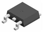
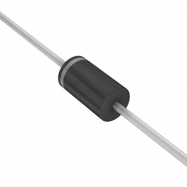
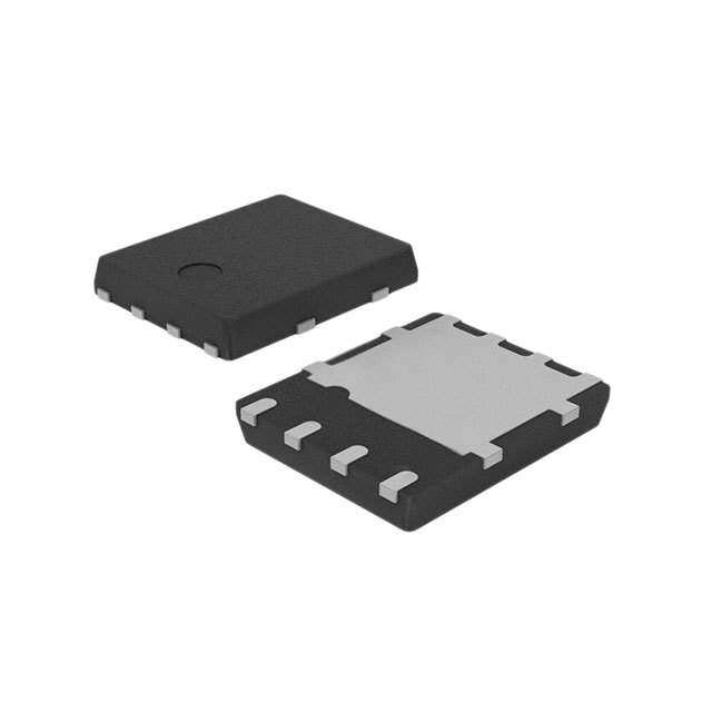
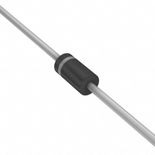
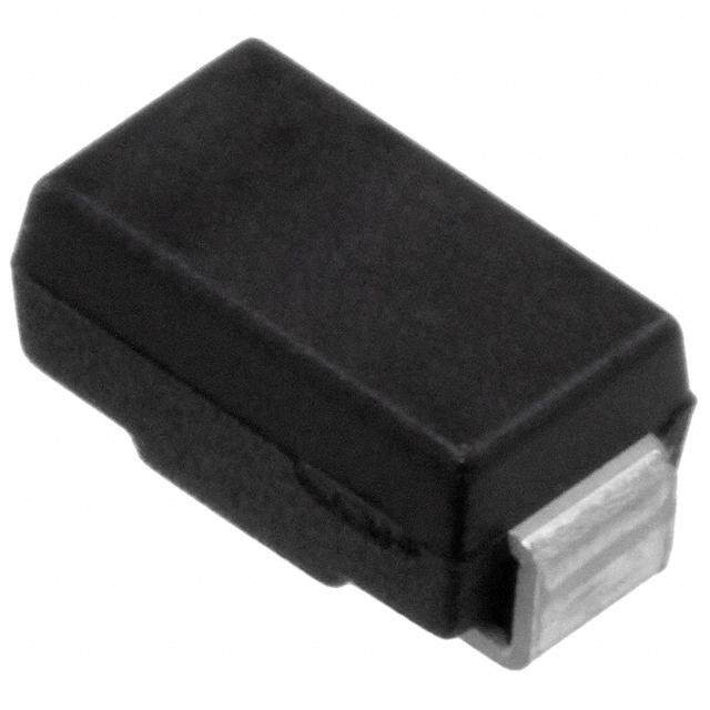
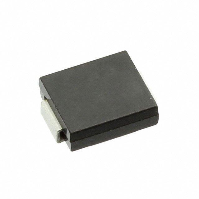
| 描述 | DIODE SCHOTTKY 40V 3A DPAK肖特基二极管与整流器 3.0 Amp 40 Volt |
| 产品分类 | 单二极管/整流器分离式半导体 |
| 品牌 | STMicroelectronics |
| 产品手册 | |
| 产品图片 |
|
| rohs | 符合RoHS无铅 / 符合限制有害物质指令(RoHS)规范要求 |
| 产品系列 | 二极管与整流器,肖特基二极管与整流器,STMicroelectronics STPS340B-TR- |
| 数据手册 | |
| 产品型号 | STPS340B-TR |
| 不同If时的电压-正向(Vf) | 630mV @ 3A |
| 不同 Vr、F时的电容 | - |
| 不同 Vr时的电流-反向漏电流 | 20µA @ 40V |
| 二极管类型 | |
| 产品 | Schottky Rectifiers |
| 产品目录页面 | |
| 产品种类 | 肖特基二极管与整流器 |
| 供应商器件封装 | D-Pak |
| 其它名称 | 497-2466-6 |
| 其它有关文件 | http://www.st.com/web/catalog/sense_power/FM64/CL1571/SC541/SS1617/PF64886?referrer=70071840 |
| 包装 | Digi-Reel® |
| 反向恢复时间(trr) | - |
| 商标 | STMicroelectronics |
| 安装类型 | 表面贴装 |
| 安装风格 | SMD/SMT |
| 封装 | Reel |
| 封装/外壳 | TO-252-3,DPak(2 引线+接片),SC-63 |
| 封装/箱体 | DPAK |
| 峰值反向电压 | 40 V |
| 工作温度-结 | 150°C (最大) |
| 工作温度范围 | + 150 C |
| 工厂包装数量 | 2500 |
| 技术 | Silicon |
| 最大反向漏泄电流 | 20 uA |
| 最大工作温度 | + 150 C |
| 最大浪涌电流 | 75 A |
| 最小工作温度 | - 65 C |
| 标准包装 | 1 |
| 正向电压下降 | 0.84 V at 6 A |
| 正向连续电流 | 3 A |
| 热阻 | 5.5°C/W Jc |
| 电压-DC反向(Vr)(最大值) | 40V |
| 电流-平均整流(Io) | 3A |
| 系列 | STPS340 |
| 速度 | 快速恢复 =< 500 ns,> 200mA(Io) |
| 配置 | Single |


- 商务部:美国ITC正式对集成电路等产品启动337调查
- 曝三星4nm工艺存在良率问题 高通将骁龙8 Gen1或转产台积电
- 太阳诱电将投资9.5亿元在常州建新厂生产MLCC 预计2023年完工
- 英特尔发布欧洲新工厂建设计划 深化IDM 2.0 战略
- 台积电先进制程称霸业界 有大客户加持明年业绩稳了
- 达到5530亿美元!SIA预计今年全球半导体销售额将创下新高
- 英特尔拟将自动驾驶子公司Mobileye上市 估值或超500亿美元
- 三星加码芯片和SET,合并消费电子和移动部门,撤换高东真等 CEO
- 三星电子宣布重大人事变动 还合并消费电子和移动部门
- 海关总署:前11个月进口集成电路产品价值2.52万亿元 增长14.8%


PDF Datasheet 数据手册内容提取
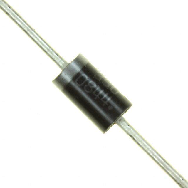
STPS340 Datasheet 40 V, 3 A power Schottky rectifier Features • Very small conduction losses • Negligible switching losses • Low forward voltage drop • Low thermal resistance • Extremely fast switching • Surface mount package • Avalanche rated • ECOPACK2 component Applications • Telecom power supply • Set-top box power supply • TV power supply • Battery charger Description Single chip Schottky rectifier suited for switch mode power supplies and high frequency DC to DC converters. Packaged in SMA Flat Notch, SMB, SMB Flat, SMC and DPAK, the STPS340 is ideal Product status for surface mounting and used in low voltage, high frequency inverters, free wheeling and polarity protection applications. STPS340 Product summary Symbol Value IF(AV) 3 A VRRM 40 V T j(max.) 150 °C VF(typ.) 0.52 V DS0792 - Rev 13 - October 2019 www.st.com For further information contact your local STMicroelectronics sales office.
STPS340 Characteristics 1 Characteristics Table 1. Absolute ratings (limiting values at 25 °C, unless otherwise specified) Symbol Parameter Value Unit VRRM Repetitive peak reverse voltage 40 V IF(RMS) Forward rms current DPAK 6 A SMA Flat Notch TL = 105 °C SMB TL = 95 °C IF(AV) Average forward current, δ = 0.5, square wave SMB Flat TL = 115 °C 3 A SMC TL = 105 °C DPAK TC = 135°C SMA Flat Notch 105 A IFSM Surge non repetitive forward current tp = 10 ms sinusoidal All others 75 A PARM Repetitive peak avalanche power tp = 10 µs, Tj = 125 °C 90 W Tstg Storage temperature range -65 to +150 °C Tj Maximum operating junction temperature(1) +150 °C 1. (dPtot/dTj) < (1/Rth(j-a)) condition to avoid thermal runaway for a diode on its own heatsink. Table 2. Thermal resistance parameter Symbol Parameter Max. value Unit SMA Flat Notch 20 SMB 25 Rth(j-l) Junction to lead SMB Flat 15 °C/W SMC 20 Rth(j-c) Junction to case DPAK 5.5 For more information, please refer to the following application note : • AN5088 : Rectifiers thermal management, handling and mounting recommendations Table 3. Static electrical characteristics Symbol Parameter Test conditions Min. Typ. Max. Unit Tj = 25 °C - 20 µA IR(1) Reverse leakage current VR = VRRM Tj = 125 °C - 2 10 mA Tj = 25 °C - 0.63 IF = 3 A Tj = 125 °C - 0.52 0.57 VF(1) Forward voltage drop V Tj = 25 °C - 0.84 IF = 6 A Tj = 125 °C - 0.63 0.72 1. Pulse test: tp = 380 µs, δ < 2% DS0792 - Rev 13 page 2/19
STPS340 Characteristics To evaluate the conduction losses, use the following equation: P = 0.42 x I + 0.050 x I 2 F(AV) F (RMS) For more information, please refer to the following application notes related to the power losses : • AN604: Calculation of conduction losses in a power rectifier • AN4021: Calculation of reverse losses on a power diode DS0792 - Rev 13 page 3/19
STPS340 Characteristics (curves) 1.1 Characteristics (curves) Figure 1. Average forward power dissipation versus Figure 2. Average forward current versus ambient average forward current temperature (δ = 0.5) (SMB, SMC, DPAK) 2.5PF(AV)(W) 3.5 IF(AV()A) DPAK δ= 0.1 δ= 0.2 δ= 0.5 Rth(j-a) = Rth(j-c) δ= 0.05 3.0 2.0 SMB δ= 1 2.5 Rth(j-a) = Rth(j-l) 1.5 2.0 SMC Rth(j-a) = Rth(j-l) 1.0 1.5 0.5 T 1.0 Rth(j-a) = 65 °C/W T 0.5 δ=tp/T tp 0.0 0.0 0.5 1.0 1.5 2.0 2.5 3.0 3.5 4.0 0.0 δ = tP/T tP Tamb(°C) IF(AV)(A) 0 25 50 75 100 125 150 Figure 3. Average forward current versus ambient Figure 4. Normalized avalanche power derating versus temperature (δ = 0.5, SMB Flat) pulse duration (Tj = 125 °C) P (tp) ARM P (10 µs) IF(AV)(A) ARM 3.5 1 Rth(j-a) = Rth(j-l) 3.0 2.5 0.1 2.0 1.5 1.0 0.01 T 0.5 0.0 δ = tP/T tP tp(µs) 0.001 0 25 50 75 100 125 150 Tamb(°C) 1 10 100 1000 Figure 5. Relative variation of thermal impedance junction Figure 6. Relative variation of thermal impedance junction to ambient versus pulse duration (SMB) to lead versus pulse duration (SMB flat) Zth(j-a)/Rth(j-a) Zth(j-l)/Rth(j-l) 1.0 1.0 0.9 0.9 0.8 0.8 0.7 0.7 0.6 0.6 0.5 0.5 0.4 0.4 0.3 0.3 0.2 0.2 Single pulse Single pulse 0.1 0.1 0.0 0.0 1.E-02 1.E-01 1.E+00 tp(s) 1.E+01 1.E+02 1.E+03 1.E-04 1.E-03 1.E-02 tp(s) 1.E-01 1.E+00 1.E+01 DS0792 - Rev 13 page 4/19
STPS340 Characteristics (curves) Figure 7. Relative variation of thermal impedance junction Figure 8. Relative variation of thermal impedance junction to ambient versus pulse duration (SMC) to case versus pulse duration (DPAK) Zth(j-a)/Rth(j-a) Zth(j-c)/Rth(j-c) 1.0 1.0 0.9 0.9 0.8 0.8 0.7 0.7 0.6 0.6 0.5 0.5 0.4 0.4 0.3 0.3 Single pulse 0.2 0.2 Single pulse 0.1 0.1 0.0 0.0 1.E-02 1.E-01 1.E+00 tp(s)1.E+01 1.E+02 1.E+03 1.E-03 1.E-02 tp(s) 1.E-01 1.E+00 Figure 9. Reverse leakage current versus reverse voltage Figure 10. Junction capacitance versus reverse voltage applied (typical values) applied (typical values) IR(mA) C(pF) 1.E+01 1000 Tj=150°C F=1MHz VOSC=30mVRMS Tj=25°C 1.E+00 Tj=125°C Tj=100°C 1.E-01 Tj=75°C 100 1.E-02 Tj=25°C 1.E-03 10 1.E-04 0 5 10 15 20VR(V)25 30 35 40 1 V1R(0V) 100 Figure 12. Thermal resistance junction to ambient versus Figure 11. Forward voltage drop versus forward current copper surface under each lead (SMA Flat Notch) IF(A) Rth(j-a)(°C/W) 10.00 200 Epoxy printed circuit board FR4,copper thickness:35 µm SMA Flat Notch (MaxTimj=u1m25 v°aClues) 1.00 150 ((TTyyppTTiijjcc==aa11ll22vv55aa°°llCCuueess)) 100 0.10 (MaxiTmj=u2m5 °vCalues) 50 S(Cu)(cm²) 0.01 0.0 0.1 0.2 0.3 0.4 0.5 0.6 0.7 0.8 0.9 1.0 0 VF(V) 0.0 0.5 1.0 1.5 2.0 2.5 3.0 3.5 4.0 4.5 5.0 DS0792 - Rev 13 page 5/19
STPS340 Characteristics (curves) Figure 13. Thermal resistance junction to ambient versus Figure 14. Thermal resistance junction to ambient versus copper surface under each lead (SMB) copper surface under each lead (SMB flat) Rth(j-a)(°C/W) R (°C/W) th(j-a) 200 200 EpoxyprintedcircuitboardFR4,copperthickness:35µm SMB Epoxy printed circuit board FR4, eCu= 35 µm SMB flat 150 150 100 100 50 50 S(Cu)(cm²) SCu(cm²) 0 0 0.0 0.5 1.0 1.5 2.0 2.5 3.0 3.5 4.0 4.5 5.0 0.0 0.5 1.0 1.5 2.0 2.5 3.0 3.5 4.0 4.5 5.0 Figure 16. Thermal resistance junction to ambient versus Figure 15. Thermal resistance junction to ambient versus copper surface under tab (DPAK) copper surface under each lead (SMC) 160 Rth(j-a)(°C/W) 100 Rth(j-a)(°C/W) EpoxyprintedcircuitboardFR4,copperthickness:35µm DPAK 140 SMC 90 Epoxy printed circuit board, copper thickness: 35 µm 80 120 70 100 60 80 50 60 40 30 40 20 20 10 SCu(cm²) SCu(cm²) 0 0 0.0 0.5 1.0 1.5 2.0 2.5 3.0 3.5 4.0 4.5 5.0 0 5 10 15 20 25 30 35 40 DS0792 - Rev 13 page 6/19
STPS340 Package information 2 Package information In order to meet environmental requirements, ST offers these devices in different grades of ECOPACK packages, depending on their level of environmental compliance. ECOPACK specifications, grade definitions and product status are available at: www.st.com. ECOPACK is an ST trademark. 2.1 SMA Flat Notch package information • Epoxy meets UL94, V0 • Cooling method: by conduction (C) • Band indicates cathode Figure 17. SMA Flat Notch package outline DS0792 - Rev 13 page 7/19
STPS340 SMA Flat Notch package information Table 4. SMA Flat Notch package mechanical data Dimensions Ref. Millimeters Inches (for reference only) Min. Typ. Max. Min. Typ. Max. A1 0.90 1.10 0.035 0.044 A1 0.05 0.002 b 1.25 1.65 0.049 0.065 C 0.15 0.40 0.005 0.016 D 2.25 2.90 0.088 0.115 E 5.00 5.35 0.196 0.211 E1 3.95 4.60 0.155 0.182 G 2.00 0.079 G1 0.85 0.033 L 0.75 1.20 0.029 L1 0.45 0.018 L2 0.45 0.018 L3 0.05 0.002 V 8° 8° V1 8° 8° Figure 18. SMA Flat Notch recommended footprint in mm (inches) 1.20 3.12 1.20 (0.047) (0.123) (0.047) 1.52 (0.060) 5.52 (0.217) DS0792 - Rev 13 page 8/19
STPS340 SMB package information 2.2 SMB package information • Epoxy meets UL94, V0 • Lead-free package Figure 19. SMB package outline E1 D E A1 C A2 L b Table 5. SMB package mechanical data Dimensions Ref. Millimeters Inches (for reference only) Min. Max. Min. Max. A1 1.90 2.45 0.074 0.097 A2 0.05 0.20 0.001 0.008 b 1.95 2.20 0.076 0.087 c 0.15 0.40 0.005 0.016 D 3.30 3.95 0.129 0.156 E 5.10 5.60 0.200 0.221 E1 4.05 4.60 0.159 0.182 L 0.75 1.50 0.029 0.060 DS0792 - Rev 13 page 9/19
STPS340 SMB package information Figure 20. SMB recommended footprint 1.62 2.60 1.62 (0.064) (0.102) (0.064) 2.18 (0.086) 5.84 (0.230) DS0792 - Rev 13 page 10/19
STPS340 SMB Flat package information 2.3 SMB Flat package information • Epoxy meets UL94, V0 • Lead-free package Figure 21. SMB Flat package outline A c D L 2x L1 2x E E1 L2 2x b Table 6. SMB Flat mechanical data Dimensions Ref. Millimeters Inches Min. Typ. Max. Min. Typ. Max. A 0.90 1.10 0.035 0.044 b 1.95 2.20 0.076 0.087 c 0.15 0.40 0.005 0.016 D 3.30 3.95 0.129 0.156 E 5.10 5.60 0.200 0.221 E1 4.05 4.60 0.159 0.182 L 0.75 1.50 0.029 0.060 L1 0.40 0.016 L2 0.60 0.024 DS0792 - Rev 13 page 11/19
STPS340 SMB Flat package information Figure 22. Footprint recommendations, dimensions in mm (inches) 1.20 3.44 1.20 (0.047) (0.136) (0.047) 2.07 (0.082) 5.84 (0.230) millimeters (inches) DS0792 - Rev 13 page 12/19
STPS340 SMC package information 2.4 SMC package information • Epoxy meets UL94, V0 Figure 23. SMC package outline E1 D E A1 A2 b C L E2 Table 7. SMC package mechanical data Dimensions Ref. Millimeters Inches (for reference only) Min. Max. Min. Max. A1 1.90 2.45 0.0748 0.0965 A2 0.05 0.20 0.0020 0.0079 b 2.90 3.20 0.1142 0.1260 c 0.15 0.40 0.0059 0.0157 D 5.55 6.25 0.2185 0.2461 E 7.75 8.15 0.3051 0.3209 E1 6.60 7.15 0.2598 0.2815 E2 4.40 4.70 0.1732 0.1850 L 0.75 1.50 0.0295 0.0591 DS0792 - Rev 13 page 13/19
STPS340 SMC package information Figure 24. SMC recommended footprint 1.54 5.11 1.54 (0.061) (0.201) (0.061) 3.14 (0.124) 8.19 (0.323) millimeters (inches) DS0792 - Rev 13 page 14/19
STPS340 DPAK package information 2.5 DPAK package information • Epoxy meets UL 94,V0 • Cooling method: by conduction (C) Figure 25. DPAK package outline E A b4 c2 Thermal pad E1 L2 D1 D H R L4 A1 b R e e1 c A2 L1 L V2 Gauge 0.25 plane Note: This package drawing may slightly differ from the physical package. However, all the specified dimensions are guaranteed. DS0792 - Rev 13 page 15/19
STPS340 DPAK package information Table 8. DPAK package mechanical data Dimensions Ref. Millimeters Inches (for reference only) Min. Max. Min. Max. A 2.18 2.40 0.085 0.094 A1 0.90 1.10 0.035 0.043 A2 0.03 0.23 0.001 0.009 b 0.64 0.90 0.025 0.035 b4 4.95 5.46 0.194 0.215 c 0.46 0.61 0.018 0.024 c2 0.46 0.60 0.018 0.023 D 5.97 6.22 0.235 0.244 D1 4.95 5.60 0.194 0.220 E 6.35 6.73 0.250 0.265 E1 4.32 5.50 0.170 0.216 e 2.286 typ. 0.090 typ. e1 4.40 4.70 0.173 0.185 H 9.35 10.40 0.368 0.409 L 1.0 1.78 0.039 0.070 L2 1.27 0.050 L4 0.60 1.02 0.023 0.040 V2 -8° +8° -8° +8° Figure 26. DPAK recommended footprint (dimensions in mm) 12.7 6.7 3.0 3.0 A 4.572 6.7 B 1.6 The device must be positioned within 0.05 AB DS0792 - Rev 13 page 16/19
STPS340 Ordering Information 3 Ordering information Table 9. Ordering information Order code Marking Package Weight Base qty. Delivery mode STPS340AFN A340 SMA Flat Notch 0.039 g 10 000 Tape and reel STPS340U U34 SMB 0.107 g 2500 Tape and reel STPS340UF FU34 SMB Flat 0.050 g 5000 Tape and reel STPS340S S34 SMC 0.243 g 10 000 Tape and reel STPS340B-TR S3 40 DPAK 0.320 g 2500 Tape and reel DS0792 - Rev 13 page 17/19
STPS340 Revision history Table 10. Document revision history Date Version Changes Jul-2003 7 Last update. Feb-2005 8 Layout update. No content change. 08-Feb-2007 9 Reformatted to current standard. Added ECOPACK statement. Added SMBflat package. 10-Feb-2009 10 Updated ECOPACK statement. Corrected Y axis in Figure 10. 23-Apr-2015 11 Updated DPAK and reformatted to current standard. 22-Sep-2016 12 Updated DPAK package information and reformatted to current standard. 08-Oct-2019 13 Added Section 2.1 SMA Flat Notch package information. DS0792 - Rev 13 page 18/19
STPS340 IMPORTANT NOTICE – PLEASE READ CAREFULLY STMicroelectronics NV and its subsidiaries (“ST”) reserve the right to make changes, corrections, enhancements, modifications, and improvements to ST products and/or to this document at any time without notice. Purchasers should obtain the latest relevant information on ST products before placing orders. ST products are sold pursuant to ST’s terms and conditions of sale in place at the time of order acknowledgement. Purchasers are solely responsible for the choice, selection, and use of ST products and ST assumes no liability for application assistance or the design of Purchasers’ products. No license, express or implied, to any intellectual property right is granted by ST herein. Resale of ST products with provisions different from the information set forth herein shall void any warranty granted by ST for such product. ST and the ST logo are trademarks of ST. For additional information about ST trademarks, please refer to www.st.com/trademarks. All other product or service names are the property of their respective owners. Information in this document supersedes and replaces information previously supplied in any prior versions of this document. © 2019 STMicroelectronics – All rights reserved DS0792 - Rev 13 page 19/19