ICGOO在线商城 > 集成电路(IC) > 嵌入式 - 微控制器 > STM8L152R8T6
 Datasheet下载
- 型号: STM8L152R8T6
- 制造商: STMicroelectronics
- 库位|库存: xxxx|xxxx
- 要求:
| 数量阶梯 | 香港交货 | 国内含税 |
| +xxxx | $xxxx | ¥xxxx |
查看当月历史价格
查看今年历史价格
STM8L152R8T6产品简介:
ICGOO电子元器件商城为您提供STM8L152R8T6由STMicroelectronics设计生产,在icgoo商城现货销售,并且可以通过原厂、代理商等渠道进行代购。 STM8L152R8T6价格参考。STMicroelectronicsSTM8L152R8T6封装/规格:嵌入式 - 微控制器, STM8 微控制器 IC STM8L EnergyLite 8-位 16MHz 64KB(64K x 8) 闪存 64-LQFP。您可以下载STM8L152R8T6参考资料、Datasheet数据手册功能说明书,资料中有STM8L152R8T6 详细功能的应用电路图电压和使用方法及教程。
STM8L152R8T6是意法半导体(STMicroelectronics)推出的一款超低功耗微控制器,属于STM8L系列。它基于高性能的STM8 8位内核,具有丰富的外设接口和多种低功耗模式,适用于对功耗要求严格的嵌入式应用。

 应用场景

1. 便携式设备:
   STM8L152R8T6因其低功耗特性,非常适合用于便携式设备,如智能手表、健康监测器、手持式医疗设备等。这些设备通常依赖电池供电,长时间运行需要低功耗支持。该微控制器可以通过灵活的电源管理模式,延长电池寿命。

2. 智能家居:
   在智能家居系统中,STM8L152R8T6可用于控制各种传感器节点,如温度传感器、湿度传感器、烟雾报警器等。其内置的ADC(模数转换器)可以精确采集环境数据,并通过串行通信接口(如UART、SPI、I2C)将数据传输到网关或云端进行处理。

3. 工业自动化:
   该微控制器在工业自动化领域也有广泛应用,例如用于电机控制、传感器数据采集、远程监控等。其丰富的定时器资源和PWM功能使得它可以高效地控制电机速度和位置,同时保持低功耗。

4. 消费电子产品:
   STM8L152R8T6适用于各种消费电子产品,如遥控器、电子玩具、智能家电等。它的小封装和低功耗特点使其能够在这些产品中实现更长的待机时间和更小的体积设计。

5. 物联网(IoT)终端:
   在物联网应用中,STM8L152R8T6可以用作边缘计算节点,负责数据采集、预处理和传输。其低功耗特性和丰富的外设接口使得它能够适应各种物联网应用场景,如环境监测、农业灌溉、智能交通等。

6. 安全与监控系统:
   该微控制器还可以用于安全监控系统中的门禁控制、摄像头控制等。其低功耗模式可以在不活跃时自动进入睡眠状态,进一步节省能源。

总之,STM8L152R8T6凭借其低功耗、高集成度和丰富的外设接口,在多个领域都有广泛的应用前景,尤其适合对功耗敏感的嵌入式系统。
| 参数 | 数值 |
| A/D位大小 | 12 bit |
| 产品目录 | 集成电路 (IC)半导体 |
| 描述 | MCU 8BIT 32K FLASH 64LQFP8位微控制器 -MCU STM8L Ultra LP 8-Bit 64-Pin 64kB Flash |
| EEPROM容量 | 2K x 8 |
| 产品分类 | |
| I/O数 | 54 |
| 品牌 | STMicroelectronics |
| 产品手册 | |
| 产品图片 |
|
| rohs | 符合RoHS无铅 / 符合限制有害物质指令(RoHS)规范要求 |
| 产品系列 | 嵌入式处理器和控制器,微控制器 - MCU,8位微控制器 -MCU,STMicroelectronics STM8L152R8T6STM8L EnergyLite |
| 数据手册 | |
| 产品型号 | STM8L152R8T6 |
| RAM容量 | 4K x 8 |
| 产品培训模块 | http://www.digikey.cn/PTM/IndividualPTM.page?site=cn&lang=zhs&ptm=30015http://www.digikey.cn/PTM/IndividualPTM.page?site=cn&lang=zhs&ptm=30339 |
| 产品种类 | 8位微控制器 -MCU |
| 供应商器件封装 | 64-LQFP |
| 其它名称 | 497-11575 |
| 其它有关文件 | http://www.st.com/web/catalog/mmc/FM141/SC1244/SS1336/LN1570/PF250426?referrer=70071840http://www.st.com/web/catalog/mmc/FM141/SC1544/SS1375/LN1576/PF250426?referrer=70071840 |
| 包装 | 托盘 |
| 可用A/D通道 | 28 |
| 可编程输入/输出端数量 | 54 |
| 商标 | STMicroelectronics |
| 处理器系列 | STM8L15xR8 |
| 外设 | 高级欠压探测/复位,DMA,IR,LCD,POR,PWM,WDT |
| 安装风格 | SMD/SMT |
| 定时器数量 | 5 Timer |
| 封装 | Tray |
| 封装/外壳 | 64-LQFP |
| 封装/箱体 | LQFP-64 |
| 工作温度 | -40°C ~ 85°C |
| 工作电源电压 | 1.8 V to 3.6 V |
| 工厂包装数量 | 160 |
| 振荡器类型 | 内部 |
| 接口类型 | I2C, SPI, USART |
| 数据RAM大小 | 4 kB |
| 数据Ram类型 | RAM |
| 数据ROM大小 | 2 kB |
| 数据Rom类型 | EEPROM |
| 数据总线宽度 | 8 bit |
| 数据转换器 | A/D 28x12b,D/A 2x12 |
| 最大工作温度 | + 85 C |
| 最大时钟频率 | 16 MHz |
| 最小工作温度 | - 40 C |
| 标准包装 | 160 |
| 核心 | STM8 |
| 核心处理器 | STM8 |
| 核心尺寸 | 8-位 |
| 片上ADC | Yes |
| 片上DAC | Without DAC |
| 特色产品 | http://www.digikey.com/product-highlights/cn/zh/segger-microcontroller-systems-flasher-tools/3226 |
| 电压-电源(Vcc/Vdd) | 1.8 V ~ 3.6 V |
| 电源电压-最大 | 3.6 V |
| 电源电压-最小 | 1.8 V |
| 程序存储器大小 | 64 kB |
| 程序存储器类型 | Flash |
| 程序存储容量 | 64KB(64K x 8) |
| 系列 | STM8L152R8 |
| 输入/输出端数量 | 54 I/O |
| 连接性 | I²C, IrDA, SPI, UART/USART |
| 速度 | 16MHz |


- 商务部:美国ITC正式对集成电路等产品启动337调查
- 曝三星4nm工艺存在良率问题 高通将骁龙8 Gen1或转产台积电
- 太阳诱电将投资9.5亿元在常州建新厂生产MLCC 预计2023年完工
- 英特尔发布欧洲新工厂建设计划 深化IDM 2.0 战略
- 台积电先进制程称霸业界 有大客户加持明年业绩稳了
- 达到5530亿美元!SIA预计今年全球半导体销售额将创下新高
- 英特尔拟将自动驾驶子公司Mobileye上市 估值或超500亿美元
- 三星加码芯片和SET,合并消费电子和移动部门,撤换高东真等 CEO
- 三星电子宣布重大人事变动 还合并消费电子和移动部门
- 海关总署:前11个月进口集成电路产品价值2.52万亿元 增长14.8%


PDF Datasheet 数据手册内容提取
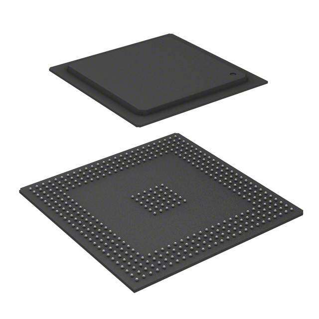
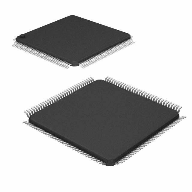
STM8L151x6/8 STM8L152x6/8 8-bit ultra-low-power MCU, up to 64-KB Flash, 2-KB data EEPROM, RTC, LCD, timers, USARTs, I2C, SPIs, ADC, DAC, comparators Datasheet - production data Features CSP • Operating conditions – Operating power supply: 1.65 to 3.6 V LQFP80 (14x14mm) (without BOR), 1.8 to 3.6 V (with BOR) LQFP64 (10x10mm) UFQFPN48 WLCSP32 LQFP48 (7x7mm) 7x7mm 1.913x3.329mm – Temp. range: -40 to 85, 105 or 125 °C • Low-power features • Memories – Up to 64-Kbytes of Flash memory with up – 5 low-power modes: Wait, Low-power run to 2 Kbytes of data EEPROM with ECC and (5.9 µA), Low-power wait (3 µA), Active- RWW halt with full RTC (1.4 µA), Halt (400 nA) – Flexible write/read protection modes – Consumption: 200 µA/MHz+330 µA – Up to 4 Kbytes of RAM – Fast wake up from Halt mode (4.7 µs) – Ultra low leakage per I/0: 50 nA • 2 ultra-low-power comparators • Advanced STM8 core – 1 with fixed threshold and 1 rail to rail – Wake up capability – Harvard architecture and 3-stage pipeline – Max freq: 16 MHz, 16 CISC MIPS peak • Timers – Up to 40 external interrupt sources – Three 16-bit timers with 2 channels (IC, OC, PWM), quadrature encoder • Reset and supply management – One 16-bit advanced control timer with 3 – Low-power, ultra safe BOR reset with five channels, supporting motor control programmable thresholds – One 8-bit timer with 7-bit prescaler – Ultra-low-power POR/PDR – One window, one independent watchdog – Programmable voltage detector (PVD) – Beeper timer with 1, 2 or 4 kHz frequencies • Clock management • Communication interfaces – 32 kHz and 1-16 MHz crystal oscillators – Two synchronous serial interface (SPI) – Internal 16 MHz factory-trimmed RC and – Fast I2C 400 kHz SMBus and PMBus 38 kHz low consumption RC – Three USARTs (ISO 7816 interface + IrDA) – Clock security system • Low-power RTC • Up to 67 I/Os, all mappable on interrupt vectors – BCD calendar with alarm interrupt • Up to 16 capacitive sensing channels supporting touchkey, proximity, linear touch – Digital calibration with +/- 0.5ppm accuracy and rotary touch sensors – Advanced anti-tamper detection • Fast on-chip programming and non-intrusive • LCD: 8x40 or 4x44 w/ step-up converter debugging with SWIM, Bootloader using • DMA USART – 4 ch. for ADC, DACs, SPIs, I2C, USARTs, • 96-bit unique ID Timers, 1 ch. for memory-to-memory • 2x12-bit DAC (dual mode) with output buffer • 12-bit ADC up to 1 Msps/28 channels – Temp. sensor and internal ref. voltage May 2018 DS6948 Rev 11 1/147 This is information on a product in full production. www.st.com
STM8L151x6/8 STM8L152x6/8 Table 1. Device summary Reference Part number STM8L151x6/8 STM8L151R6, STM8L151C8, STM8L151M8, STM8L151R8 STM8L152x6/8 STM8L152R6, STM8L152C8, STM8L152K8, STM8L152M8, STM8L152R8 2/147 DS6948 Rev 11
STM8L151x6/8 STM8L152x6/8 Contents Contents 1 Introduction . . . . . . . . . . . . . . . . . . . . . . . . . . . . . . . . . . . . . . . . . . . . . . . 10 2 Description . . . . . . . . . . . . . . . . . . . . . . . . . . . . . . . . . . . . . . . . . . . . . . . . 10 2.1 STM8L ultra-low-power 8-bit family benefits . . . . . . . . . . . . . . . . . . . . . . .11 2.2 Device overview . . . . . . . . . . . . . . . . . . . . . . . . . . . . . . . . . . . . . . . . . . . . 12 2.3 Ultra-low-power continuum . . . . . . . . . . . . . . . . . . . . . . . . . . . . . . . . . . . . 13 3 Functional overview . . . . . . . . . . . . . . . . . . . . . . . . . . . . . . . . . . . . . . . . 14 3.1 Low-power modes . . . . . . . . . . . . . . . . . . . . . . . . . . . . . . . . . . . . . . . . . . 15 3.2 Central processing unit STM8 . . . . . . . . . . . . . . . . . . . . . . . . . . . . . . . . . 16 3.2.1 Advanced STM8 Core . . . . . . . . . . . . . . . . . . . . . . . . . . . . . . . . . . . . . . 16 3.2.2 Interrupt controller . . . . . . . . . . . . . . . . . . . . . . . . . . . . . . . . . . . . . . . . . 16 3.3 Reset and supply management . . . . . . . . . . . . . . . . . . . . . . . . . . . . . . . . 17 3.3.1 Power supply scheme . . . . . . . . . . . . . . . . . . . . . . . . . . . . . . . . . . . . . . 17 3.3.2 Power supply supervisor . . . . . . . . . . . . . . . . . . . . . . . . . . . . . . . . . . . . 17 3.3.3 Voltage regulator . . . . . . . . . . . . . . . . . . . . . . . . . . . . . . . . . . . . . . . . . . 18 3.4 Clock management . . . . . . . . . . . . . . . . . . . . . . . . . . . . . . . . . . . . . . . . . 18 3.5 Low-power real-time clock . . . . . . . . . . . . . . . . . . . . . . . . . . . . . . . . . . . . 19 3.6 LCD (Liquid crystal display) . . . . . . . . . . . . . . . . . . . . . . . . . . . . . . . . . . . 20 3.7 Memories . . . . . . . . . . . . . . . . . . . . . . . . . . . . . . . . . . . . . . . . . . . . . . . . . 20 3.8 DMA . . . . . . . . . . . . . . . . . . . . . . . . . . . . . . . . . . . . . . . . . . . . . . . . . . . . . 20 3.9 Analog-to-digital converter . . . . . . . . . . . . . . . . . . . . . . . . . . . . . . . . . . . . 21 3.10 Digital-to-analog converter . . . . . . . . . . . . . . . . . . . . . . . . . . . . . . . . . . . . 21 3.11 Ultra-low-power comparators . . . . . . . . . . . . . . . . . . . . . . . . . . . . . . . . . . 21 3.12 System configuration controller and routing interface . . . . . . . . . . . . . . . 22 3.13 Touch sensing . . . . . . . . . . . . . . . . . . . . . . . . . . . . . . . . . . . . . . . . . . . . . 22 3.14 Timers . . . . . . . . . . . . . . . . . . . . . . . . . . . . . . . . . . . . . . . . . . . . . . . . . . . 22 3.14.1 16-bit advanced control timer (TIM1) . . . . . . . . . . . . . . . . . . . . . . . . . . . 23 3.14.2 16-bit general purpose timers (TIM2, TIM3, TIM5) . . . . . . . . . . . . . . . . 23 3.14.3 8-bit basic timer (TIM4) . . . . . . . . . . . . . . . . . . . . . . . . . . . . . . . . . . . . . 23 3.15 Watchdog timers . . . . . . . . . . . . . . . . . . . . . . . . . . . . . . . . . . . . . . . . . . . 23 3.15.1 Window watchdog timer . . . . . . . . . . . . . . . . . . . . . . . . . . . . . . . . . . . . . 23 DS6948 Rev 11 3/147 5
Contents STM8L151x6/8 STM8L152x6/8 3.15.2 Independent watchdog timer . . . . . . . . . . . . . . . . . . . . . . . . . . . . . . . . . 23 3.16 Beeper . . . . . . . . . . . . . . . . . . . . . . . . . . . . . . . . . . . . . . . . . . . . . . . . . . . 24 3.17 Communication interfaces . . . . . . . . . . . . . . . . . . . . . . . . . . . . . . . . . . . . 24 3.17.1 SPI . . . . . . . . . . . . . . . . . . . . . . . . . . . . . . . . . . . . . . . . . . . . . . . . . . . . . 24 3.17.2 I2C . . . . . . . . . . . . . . . . . . . . . . . . . . . . . . . . . . . . . . . . . . . . . . . . . . . . . 24 3.17.3 USART . . . . . . . . . . . . . . . . . . . . . . . . . . . . . . . . . . . . . . . . . . . . . . . . . . 25 3.18 Infrared (IR) interface . . . . . . . . . . . . . . . . . . . . . . . . . . . . . . . . . . . . . . . . 25 3.19 Development support . . . . . . . . . . . . . . . . . . . . . . . . . . . . . . . . . . . . . . . . 25 4 Pin description . . . . . . . . . . . . . . . . . . . . . . . . . . . . . . . . . . . . . . . . . . . . 26 5 Memory and register map . . . . . . . . . . . . . . . . . . . . . . . . . . . . . . . . . . . . 41 5.1 Memory mapping . . . . . . . . . . . . . . . . . . . . . . . . . . . . . . . . . . . . . . . . . . . 41 5.2 Register map . . . . . . . . . . . . . . . . . . . . . . . . . . . . . . . . . . . . . . . . . . . . . . 42 6 Interrupt vector mapping . . . . . . . . . . . . . . . . . . . . . . . . . . . . . . . . . . . . 62 7 Option bytes . . . . . . . . . . . . . . . . . . . . . . . . . . . . . . . . . . . . . . . . . . . . . . 64 8 Unique ID . . . . . . . . . . . . . . . . . . . . . . . . . . . . . . . . . . . . . . . . . . . . . . . . . 67 9 Electrical parameters . . . . . . . . . . . . . . . . . . . . . . . . . . . . . . . . . . . . . . . 68 9.1 Parameter conditions . . . . . . . . . . . . . . . . . . . . . . . . . . . . . . . . . . . . . . . . 68 9.1.1 Minimum and maximum values . . . . . . . . . . . . . . . . . . . . . . . . . . . . . . . 68 9.1.2 Typical values . . . . . . . . . . . . . . . . . . . . . . . . . . . . . . . . . . . . . . . . . . . . 68 9.1.3 Typical curves . . . . . . . . . . . . . . . . . . . . . . . . . . . . . . . . . . . . . . . . . . . . 68 9.1.4 Loading capacitor . . . . . . . . . . . . . . . . . . . . . . . . . . . . . . . . . . . . . . . . . 68 9.1.5 Pin input voltage . . . . . . . . . . . . . . . . . . . . . . . . . . . . . . . . . . . . . . . . . . 69 9.2 Absolute maximum ratings . . . . . . . . . . . . . . . . . . . . . . . . . . . . . . . . . . . . 69 9.3 Operating conditions . . . . . . . . . . . . . . . . . . . . . . . . . . . . . . . . . . . . . . . . 71 9.3.1 General operating conditions . . . . . . . . . . . . . . . . . . . . . . . . . . . . . . . . . 71 9.3.2 Embedded reset and power control block characteristics . . . . . . . . . . 72 9.3.3 Supply current characteristics . . . . . . . . . . . . . . . . . . . . . . . . . . . . . . . . 75 9.3.4 Clock and timing characteristics . . . . . . . . . . . . . . . . . . . . . . . . . . . . . . 90 9.3.5 Memory characteristics . . . . . . . . . . . . . . . . . . . . . . . . . . . . . . . . . . . . . 95 9.3.6 I/O current injection characteristics . . . . . . . . . . . . . . . . . . . . . . . . . . . . 97 9.3.7 I/O port pin characteristics . . . . . . . . . . . . . . . . . . . . . . . . . . . . . . . . . . . 97 4/147 DS6948 Rev 11
STM8L151x6/8 STM8L152x6/8 Contents 9.3.8 Communication interfaces . . . . . . . . . . . . . . . . . . . . . . . . . . . . . . . . . . 105 9.3.9 LCD controller (STM8L152x6/8 only) . . . . . . . . . . . . . . . . . . . . . . . . . 110 9.3.10 Embedded reference voltage . . . . . . . . . . . . . . . . . . . . . . . . . . . . . . . . 111 9.3.11 Temperature sensor . . . . . . . . . . . . . . . . . . . . . . . . . . . . . . . . . . . . . . . 112 9.3.12 Comparator characteristics . . . . . . . . . . . . . . . . . . . . . . . . . . . . . . . . . 112 9.3.13 12-bit DAC characteristics . . . . . . . . . . . . . . . . . . . . . . . . . . . . . . . . . . 114 9.3.14 12-bit ADC1 characteristics . . . . . . . . . . . . . . . . . . . . . . . . . . . . . . . . . 116 9.3.15 EMC characteristics . . . . . . . . . . . . . . . . . . . . . . . . . . . . . . . . . . . . . . . 122 9.4 Thermal characteristics . . . . . . . . . . . . . . . . . . . . . . . . . . . . . . . . . . . . . 124 10 Package information . . . . . . . . . . . . . . . . . . . . . . . . . . . . . . . . . . . . . . . 125 10.1 LQFP80 package information . . . . . . . . . . . . . . . . . . . . . . . . . . . . . . . . . 125 10.2 LQFP64 package information . . . . . . . . . . . . . . . . . . . . . . . . . . . . . . . . . 129 10.3 LQFP48 package information . . . . . . . . . . . . . . . . . . . . . . . . . . . . . . . . . 132 10.4 UFQFPN48 package information . . . . . . . . . . . . . . . . . . . . . . . . . . . . . . 136 10.5 WLCSP32 package information . . . . . . . . . . . . . . . . . . . . . . . . . . . . . . . 139 11 Ordering information . . . . . . . . . . . . . . . . . . . . . . . . . . . . . . . . . . . . . . 142 12 Revision history . . . . . . . . . . . . . . . . . . . . . . . . . . . . . . . . . . . . . . . . . . 143 DS6948 Rev 11 5/147 5
List of tables STM8L151x6/8 STM8L152x6/8 List of tables Table 1. Device summary. . . . . . . . . . . . . . . . . . . . . . . . . . . . . . . . . . . . . . . . . . . . . . . . . . . . . . . . . . 2 Table 2. High-density and medium+ density STM8L15xx6/8 low power device features and peripheral counts. . . . . . . . . . . . . . . . . . . . . . . . . . . . . . . . . . . . . . . . . . . . . . . . . . . . . . . . 12 Table 3. Timer feature comparison. . . . . . . . . . . . . . . . . . . . . . . . . . . . . . . . . . . . . . . . . . . . . . . . . . 22 Table 4. Legend/abbreviation. . . . . . . . . . . . . . . . . . . . . . . . . . . . . . . . . . . . . . . . . . . . . . . . . . . . . . 30 Table 5. High-density and medium+ density STM8L15x pin description . . . . . . . . . . . . . . . . . . . . . 30 Table 6. Flash and RAM boundary addresses. . . . . . . . . . . . . . . . . . . . . . . . . . . . . . . . . . . . . . . . . 42 Table 7. Factory conversion registers. . . . . . . . . . . . . . . . . . . . . . . . . . . . . . . . . . . . . . . . . . . . . . . . 42 Table 8. I/O port hardware register map. . . . . . . . . . . . . . . . . . . . . . . . . . . . . . . . . . . . . . . . . . . . . . 42 Table 9. General hardware register map . . . . . . . . . . . . . . . . . . . . . . . . . . . . . . . . . . . . . . . . . . . . . 44 Table 10. CPU/SWIM/debug module/interrupt controller registers. . . . . . . . . . . . . . . . . . . . . . . . . . . 60 Table 11. Interrupt mapping . . . . . . . . . . . . . . . . . . . . . . . . . . . . . . . . . . . . . . . . . . . . . . . . . . . . . . . . 62 Table 12. Option byte addresses . . . . . . . . . . . . . . . . . . . . . . . . . . . . . . . . . . . . . . . . . . . . . . . . . . . . 64 Table 13. Option byte description. . . . . . . . . . . . . . . . . . . . . . . . . . . . . . . . . . . . . . . . . . . . . . . . . . . . 65 Table 14. Unique ID registers (96 bits). . . . . . . . . . . . . . . . . . . . . . . . . . . . . . . . . . . . . . . . . . . . . . . . 67 Table 15. Voltage characteristics . . . . . . . . . . . . . . . . . . . . . . . . . . . . . . . . . . . . . . . . . . . . . . . . . . . . 69 Table 16. Current characteristics . . . . . . . . . . . . . . . . . . . . . . . . . . . . . . . . . . . . . . . . . . . . . . . . . . . . 70 Table 17. Thermal characteristics. . . . . . . . . . . . . . . . . . . . . . . . . . . . . . . . . . . . . . . . . . . . . . . . . . . . 70 Table 18. General operating conditions . . . . . . . . . . . . . . . . . . . . . . . . . . . . . . . . . . . . . . . . . . . . . . . 71 Table 19. Embedded reset and power control block characteristics. . . . . . . . . . . . . . . . . . . . . . . . . . 72 Table 20. Total current consumption in Run mode. . . . . . . . . . . . . . . . . . . . . . . . . . . . . . . . . . . . . . . 75 Table 21. Total current consumption in Wait mode . . . . . . . . . . . . . . . . . . . . . . . . . . . . . . . . . . . . . . 78 Table 22. Total current consumption and timing in Low-power run mode at VDD = 1.65 V to 3.6 V . 81 Table 23. Total current consumption in Low-power wait mode at VDD = 1.65 V to 3.6 V . . . . . . . . . 83 Table 24. Total current consumption and timing in Active-halt mode at VDD = 1.65 V to 3.6 V. . . . . . . . . . . . . . . . . . . . . . . . . . . . . . . . . . . . . . . . . . . . . . . . . . 85 Table 25. Typical current consumption in Active-halt mode, RTC clocked by LSE external crystal. . 87 Table 26. Total current consumption and timing in Halt mode at VDD = 1.65 to 3.6 V . . . . . . . . . . . 88 Table 27. Peripheral current consumption . . . . . . . . . . . . . . . . . . . . . . . . . . . . . . . . . . . . . . . . . . . . . 89 Table 28. Current consumption under external reset. . . . . . . . . . . . . . . . . . . . . . . . . . . . . . . . . . . . . 90 Table 29. HSE external clock characteristics. . . . . . . . . . . . . . . . . . . . . . . . . . . . . . . . . . . . . . . . . . . 90 Table 30. LSE external clock characteristics . . . . . . . . . . . . . . . . . . . . . . . . . . . . . . . . . . . . . . . . . . . 91 Table 31. HSE oscillator characteristics. . . . . . . . . . . . . . . . . . . . . . . . . . . . . . . . . . . . . . . . . . . . . . . 91 Table 32. LSE oscillator characteristics . . . . . . . . . . . . . . . . . . . . . . . . . . . . . . . . . . . . . . . . . . . . . . . 92 Table 33. HSI oscillator characteristics. . . . . . . . . . . . . . . . . . . . . . . . . . . . . . . . . . . . . . . . . . . . . . . . 93 Table 34. LSI oscillator characteristics. . . . . . . . . . . . . . . . . . . . . . . . . . . . . . . . . . . . . . . . . . . . . . . . 94 Table 35. RAM and hardware registers . . . . . . . . . . . . . . . . . . . . . . . . . . . . . . . . . . . . . . . . . . . . . . . 95 Table 36. Flash program and data EEPROM memory. . . . . . . . . . . . . . . . . . . . . . . . . . . . . . . . . . . . 96 Table 37. I/O current injection susceptibility. . . . . . . . . . . . . . . . . . . . . . . . . . . . . . . . . . . . . . . . . . . . 97 Table 38. I/O static characteristics . . . . . . . . . . . . . . . . . . . . . . . . . . . . . . . . . . . . . . . . . . . . . . . . . . . 98 Table 39. Output driving current (high sink ports). . . . . . . . . . . . . . . . . . . . . . . . . . . . . . . . . . . . . . . 101 Table 40. Output driving current (true open drain ports). . . . . . . . . . . . . . . . . . . . . . . . . . . . . . . . . . 101 Table 41. Output driving current (PA0 with high sink LED driver capability). . . . . . . . . . . . . . . . . . . 101 Table 42. NRST pin characteristics . . . . . . . . . . . . . . . . . . . . . . . . . . . . . . . . . . . . . . . . . . . . . . . . . 103 Table 43. SPI1 characteristics . . . . . . . . . . . . . . . . . . . . . . . . . . . . . . . . . . . . . . . . . . . . . . . . . . . . . 105 Table 44. I2C characteristics . . . . . . . . . . . . . . . . . . . . . . . . . . . . . . . . . . . . . . . . . . . . . . . . . . . . . . 108 Table 45. LCD characteristics. . . . . . . . . . . . . . . . . . . . . . . . . . . . . . . . . . . . . . . . . . . . . . . . . . . . . . 110 Table 46. Reference voltage characteristics. . . . . . . . . . . . . . . . . . . . . . . . . . . . . . . . . . . . . . . . . . . 111 6/147 DS6948 Rev 11
STM8L151x6/8 STM8L152x6/8 List of tables Table 47. TS characteristics. . . . . . . . . . . . . . . . . . . . . . . . . . . . . . . . . . . . . . . . . . . . . . . . . . . . . . . 112 Table 48. Comparator 1 characteristics . . . . . . . . . . . . . . . . . . . . . . . . . . . . . . . . . . . . . . . . . . . . . . 112 Table 49. Comparator 2 characteristics . . . . . . . . . . . . . . . . . . . . . . . . . . . . . . . . . . . . . . . . . . . . . . 113 Table 50. DAC characteristics . . . . . . . . . . . . . . . . . . . . . . . . . . . . . . . . . . . . . . . . . . . . . . . . . . . . . 114 Table 51. DAC accuracy. . . . . . . . . . . . . . . . . . . . . . . . . . . . . . . . . . . . . . . . . . . . . . . . . . . . . . . . . . 115 Table 52. DAC output on PB4-PB5-PB6 . . . . . . . . . . . . . . . . . . . . . . . . . . . . . . . . . . . . . . . . . . . . . 115 Table 53. ADC1 characteristics . . . . . . . . . . . . . . . . . . . . . . . . . . . . . . . . . . . . . . . . . . . . . . . . . . . . 116 Table 54. ADC1 accuracy with VDDA = 3.3 V to 2.5 V. . . . . . . . . . . . . . . . . . . . . . . . . . . . . . . . . . . 118 Table 55. ADC1 accuracy with VDDA = 2.4 V to 3.6 V. . . . . . . . . . . . . . . . . . . . . . . . . . . . . . . . . . . 118 Table 56. ADC1 accuracy with VDDA = VREF+ = 1.8 V to 2.4 V. . . . . . . . . . . . . . . . . . . . . . . . . . . 118 Table 57. R max for f = 16 MHz. . . . . . . . . . . . . . . . . . . . . . . . . . . . . . . . . . . . . . . . . . . . . . . 120 AIN ADC Table 58. EMS data . . . . . . . . . . . . . . . . . . . . . . . . . . . . . . . . . . . . . . . . . . . . . . . . . . . . . . . . . . . . . 122 Table 59. EMI data . . . . . . . . . . . . . . . . . . . . . . . . . . . . . . . . . . . . . . . . . . . . . . . . . . . . . . . . . . . . . 123 Table 60. ESD absolute maximum ratings. . . . . . . . . . . . . . . . . . . . . . . . . . . . . . . . . . . . . . . . . . . . 123 Table 61. Electrical sensitivities . . . . . . . . . . . . . . . . . . . . . . . . . . . . . . . . . . . . . . . . . . . . . . . . . . . . 124 Table 62. Thermal characteristics. . . . . . . . . . . . . . . . . . . . . . . . . . . . . . . . . . . . . . . . . . . . . . . . . . . 124 Table 63. LQFP80 - 80-pin, 14 x 14 mm low-profile quad flat package mechanical data . . . . . . . . . . . . . . . . . . . . . . . . . . . . . . . . . . . . . . . . . . . . . . . . . . . . . . . . 126 Table 64. LQFP64 - 64-pin, 10 x 10 mm low-profile quad flat package mechanical data. . . . . . . . . . . . . . . . . . . . . . . . . . . . . . . . . . . . . . . . . . . . . . . . . 129 Table 65. LQFP48 - 48-pin, 7 x 7 mm low-profile quad flat package mechanical data . . . . . . . . . . . . . . . . . . . . . . . . . . . . . . . . . . . . . . . . . . . . . . . . . . . . . . . . 133 Table 66. UFQFPN48 - 48-lead, 7x7 mm, 0.5 mm pitch, ultra thin fine pitch quad flat package mechanical data. . . . . . . . . . . . . . . . . . . . . . . . . . . . . . . . . . . . . . . . . . . . . . . . . 137 Table 67. WLCSP32 - 32-ball, 1.913 x 3.329 mm, 0.4 mm pitch wafer level chip scale package mechanical data. . . . . . . . . . . . . . . . . . . . . . . . . . . . . . . . . . . . . . . . . . . . . . . . . 140 Table 68. WLCSP32 recommended PCB design rules . . . . . . . . . . . . . . . . . . . . . . . . . . . . . . . . . . 141 Table 69. Ordering information scheme. . . . . . . . . . . . . . . . . . . . . . . . . . . . . . . . . . . . . . . . . . . . . . 142 Table 70. Document revision history . . . . . . . . . . . . . . . . . . . . . . . . . . . . . . . . . . . . . . . . . . . . . . . . 143 DS6948 Rev 11 7/147 7
List of figures STM8L151x6/8 STM8L152x6/8 List of figures Figure 1. High-density and medium+ density STM8L15xx6/8 device block diagram . . . . . . . . . . . . 14 Figure 2. Clock tree diagram . . . . . . . . . . . . . . . . . . . . . . . . . . . . . . . . . . . . . . . . . . . . . . . . . . . . . . . 19 Figure 3. STM8L151M8 80-pin package pinout (without LCD) . . . . . . . . . . . . . . . . . . . . . . . . . . . . . 26 Figure 4. STM8L152M8 80-pin package pinout (with LCD). . . . . . . . . . . . . . . . . . . . . . . . . . . . . . . . 26 Figure 5. STM8L151R8 and STM8L151R6 64-pin pinout (without LCD). . . . . . . . . . . . . . . . . . . . . . 27 Figure 6. STM8L152R8 and STM8L152R6 64-pin pinout (with LCD) . . . . . . . . . . . . . . . . . . . . . . . . 27 Figure 7. STM8L151C8 48-pin pinout (without LCD) . . . . . . . . . . . . . . . . . . . . . . . . . . . . . . . . . . . . 28 Figure 8. STM8L152C8 48-pin pinout (with LCD) . . . . . . . . . . . . . . . . . . . . . . . . . . . . . . . . . . . . . . . 28 Figure 9. STM8L152K8 32-ball ballout . . . . . . . . . . . . . . . . . . . . . . . . . . . . . . . . . . . . . . . . . . . . . . . 29 Figure 10. Memory map . . . . . . . . . . . . . . . . . . . . . . . . . . . . . . . . . . . . . . . . . . . . . . . . . . . . . . . . . . 41 Figure 11. Pin loading conditions. . . . . . . . . . . . . . . . . . . . . . . . . . . . . . . . . . . . . . . . . . . . . . . . . . . . . 68 Figure 12. Pin input voltage. . . . . . . . . . . . . . . . . . . . . . . . . . . . . . . . . . . . . . . . . . . . . . . . . . . . . . . . . 69 Figure 13. Power supply thresholds. . . . . . . . . . . . . . . . . . . . . . . . . . . . . . . . . . . . . . . . . . . . . . . . . . . 74 Figure 14. Typical I from RAM vs. V (HSI clock source), f =16 MHz. . . . . . . . . . . . . . . 77 DD(RUN) DD CPU Figure 15. Typical I from Flash vs. V (HSI clock source), f = 16 MHz. . . . . . . . . . . . . . 77 DD(RUN) DD CPU Figure 16. Typical I from RAM vs. V (HSI clock source), f = 16 MHz . . . . . . . . . . . . . . 80 DD(Wait) DD CPU Figure 17. Typical I from Flash (HSI clock source), f = 16 MHz . . . . . . . . . . . . . . . . . . . . 80 DD(Wait) CPU Figure 18. Typical I vs. V (LSI clock source), all peripherals OFF. . . . . . . . . . . . . . . . . . . . 82 DD(LPR) DD Figure 19. Typical I vs. V (LSI clock source), all peripherals OFF . . . . . . . . . . . . . . . . . . . 84 DD(LPW) DD Figure 20. Typical IDD(AH) vs. V (LSI clock source) . . . . . . . . . . . . . . . . . . . . . . . . . . . . . . . . . . . 87 DD Figure 21. Typical IDD(Halt) vs. V (internal reference voltage OFF). . . . . . . . . . . . . . . . . . . . . . . . 88 DD Figure 22. HSE oscillator circuit diagram. . . . . . . . . . . . . . . . . . . . . . . . . . . . . . . . . . . . . . . . . . . . . . . 92 Figure 23. LSE oscillator circuit diagram. . . . . . . . . . . . . . . . . . . . . . . . . . . . . . . . . . . . . . . . . . . . . . . 93 Figure 24. Typical HSI frequency vs. V . . . . . . . . . . . . . . . . . . . . . . . . . . . . . . . . . . . . . . . . . . . . . . 94 DD Figure 25. Typical LSI clock source frequency vs. VDD . . . . . . . . . . . . . . . . . . . . . . . . . . . . . . . . . . . 95 Figure 26. Typical VIL and VIH vs. VDD (standard I/Os). . . . . . . . . . . . . . . . . . . . . . . . . . . . . . . . . . . 99 Figure 27. Typical VIL and VIH vs. VDD (true open drain I/Os). . . . . . . . . . . . . . . . . . . . . . . . . . . . . . 99 Figure 28. Typical pull-up resistance R vs. V with VIN=VSS. . . . . . . . . . . . . . . . . . . . . . . . . . . 100 PU DD Figure 29. Typical pull-up current I vs. V with VIN=VSS . . . . . . . . . . . . . . . . . . . . . . . . . . . . . . 100 pu DD Figure 30. Typical VOL @ VDD = 3.0 V (high sink ports) . . . . . . . . . . . . . . . . . . . . . . . . . . . . . . . . . 102 Figure 31. Typical VOL @ VDD = 1.8 V (high sink ports) . . . . . . . . . . . . . . . . . . . . . . . . . . . . . . . . . 102 Figure 32. Typical VOL @ VDD = 3.0 V (true open drain ports) . . . . . . . . . . . . . . . . . . . . . . . . . . . . 102 Figure 33. Typical VOL @ VDD = 1.8 V (true open drain ports) . . . . . . . . . . . . . . . . . . . . . . . . . . . . 102 Figure 34. Typical VDD - VOH @ VDD = 3.0 V (high sink ports). . . . . . . . . . . . . . . . . . . . . . . . . . . . 102 Figure 35. Typical VDD - VOH @ VDD = 1.8 V (high sink ports). . . . . . . . . . . . . . . . . . . . . . . . . . . . 102 Figure 36. Typical NRST pull-up resistance R vs. V . . . . . . . . . . . . . . . . . . . . . . . . . . . . . . . . . 103 PU DD Figure 37. Typical NRST pull-up current I vs. V . . . . . . . . . . . . . . . . . . . . . . . . . . . . . . . . . . . . 104 pu DD Figure 38. Recommended NRST pin configuration. . . . . . . . . . . . . . . . . . . . . . . . . . . . . . . . . . . . . . 104 Figure 39. SPI1 timing diagram - slave mode and CPHA=0 . . . . . . . . . . . . . . . . . . . . . . . . . . . . . . . 106 Figure 40. SPI1 timing diagram - slave mode and CPHA=1 . . . . . . . . . . . . . . . . . . . . . . . . . . . . . . . 106 Figure 41. SPI1 timing diagram - master mode. . . . . . . . . . . . . . . . . . . . . . . . . . . . . . . . . . . . . . . . . 107 Figure 42. Typical application with I2C bus and timing diagram . . . . . . . . . . . . . . . . . . . . . . . . . . . . 109 Figure 43. ADC1 accuracy characteristics. . . . . . . . . . . . . . . . . . . . . . . . . . . . . . . . . . . . . . . . . . . . . 119 Figure 44. Typical connection diagram using the ADC . . . . . . . . . . . . . . . . . . . . . . . . . . . . . . . . . . . 119 Figure 45. Maximum dynamic current consumption on V supply pin during ADC REF+ conversion . . . . . . . . . . . . . . . . . . . . . . . . . . . . . . . . . . . . . . . . . . . . . . . . . . . . . . . . . . . . 120 Figure 46. Power supply and reference decoupling (V not connected to V ). . . . . . . . . . . . . 121 REF+ DDA Figure 47. Power supply and reference decoupling (VREF+ connected to VDDA). . . . . . . . . . . . . . 121 8/147 DS6948 Rev 11
STM8L151x6/8 STM8L152x6/8 List of figures Figure 48. LQFP80 - 80-pin, 14 x 14 mm low-profile quad flat package outline . . . . . . . . . . . . . . . . 125 Figure 49. LQFP80 - 80-pin, 14 x 14 mm low-profile quad flat package recommended footprint. . . . . . . . . . . . . . . . . . . . . . . . . . . . . . . . . . . . . . . . . . . . . . . . . . . 127 Figure 50. LQFP80 marking example (package top view) . . . . . . . . . . . . . . . . . . . . . . . . . . . . . . . . 128 Figure 51. LQFP64 - 64-pin, 10 x 10 mm low-profile quad flat package outline . . . . . . . . . . . . . . . . 129 Figure 52. LQFP64 - 64-pin, 10 x 10 mm low-profile quad flat package recommended footprint. . . . . . . . . . . . . . . . . . . . . . . . . . . . . . . . . . . . . . . . . . . . . . . . . . . 130 Figure 53. LQFP64 marking example (package top view) . . . . . . . . . . . . . . . . . . . . . . . . . . . . . . . . 131 Figure 54. LQFP48 - 48-pin, 7 x 7 mm low-profile quad flat package outline . . . . . . . . . . . . . . . . . . 132 Figure 55. LQFP48 - 48-pin, 7 x 7 mm low-profile quad flat package recommended footprint. . . . . . . . . . . . . . . . . . . . . . . . . . . . . . . . . . . . . . . . . . . . . . . . . . . 134 Figure 56. LQFP48 marking example (package top view). . . . . . . . . . . . . . . . . . . . . . . . . . . . . . . . . 135 Figure 57. UFQFPN48 - 48-lead, 7x7 mm, 0.5 mm pitch, ultra thin fine pitch quad flat package outline. . . . . . . . . . . . . . . . . . . . . . . . . . . . . . . . . . . . . . . . . . . . . . . . . . . . . . . . . 136 Figure 58. UFQFPN48 - 48-lead, 7x7 mm, 0.5 mm pitch, ultra thin fine pitch quad flat package recommended footprint . . . . . . . . . . . . . . . . . . . . . . . . . . . . . . . . . . . . . . . . . . . 137 Figure 59. UFQFPN48 marking example (package top view) . . . . . . . . . . . . . . . . . . . . . . . . . . . . . . 138 Figure 60. WLCSP32 - 32-ball, 1.913 x 3.329 mm, 0.4 mm pitch wafer level chip scale package outline. . . . . . . . . . . . . . . . . . . . . . . . . . . . . . . . . . . . . . . . . . . . . . . . . . . . . . . . . 139 Figure 61. WLCSP32 - 32-ball, 1.913 x 3.329 mm, 0.4 mm pitch wafer level chip scale package recommended footprint . . . . . . . . . . . . . . . . . . . . . . . . . . . . . . . . . . . . . . . . . . . 140 DS6948 Rev 11 9/147 9
Introduction STM8L151x6/8 STM8L152x6/8 1 Introduction This document describes the features, pinout, mechanical data and ordering information for: devices. • High-density STM8L15xxx devices: STM8L151x8 and STM8L152x8 microcontrollers with a Flash memory density of 64 Kbyte. • Medium+ density STM8L15xxx devices: STM8L151R6 and STM8L152R6 microcontrollers with Flash memory density of 32 Kbyte. For further details on the STMicroelectronics ultra-low-power family please refer to Section 2.3: Ultra-low-power continuum on page 13. For detailed information on device operation and registers, refer to the reference manual (RM0031). For information on to the Flash program memory and data EEPROM, refer to the programming manual (PM0054). For information on the debug module and SWIM (single wire interface module), refer to the STM8 SWIM communication protocol and debug module user manual (UM0470). For information on the STM8 core, refer to the STM8 CPU programming manual (PM0044). 2 Description The high-density and medium+ density STM8L15xx6/8 ultra-low-power devices feature an enhanced STM8 CPU core providing increased processing power (up to 16 MIPS at 16 MHz) while maintaining the advantages of a CISC architecture with improved code density, a 24-bit linear addressing space and an optimized architecture for low-power operations. The family includes an integrated debug module with a hardware interface (SWIM) which allows non-intrusive in-application debugging and ultrafast Flash programming. All high-density and medium+ density STM8L15xx6/8 microcontrollers feature embedded data EEPROM and low-power low-voltage single-supply program Flash memory. The devices incorporate an extensive range of enhanced I/Os and peripherals, a 12-bit ADC, two DACs, two comparators, a real-time clock, four 16-bit timers, one 8-bit timer, as well as standard communication interfaces such as two SPIs, an I2C interface, and three USARTs. A 8x40 or 4x44-segment LCD is available on the STM8L152x8 devices. The modular design of the peripheral set allows the same peripherals to be found in different ST microcontroller families including 32-bit families. This makes any transition to a different family very easy, and simplified even more by the use of a common set of development tools. 10/147 DS6948 Rev 11
STM8L151x6/8 STM8L152x6/8 Description 2.1 STM8L ultra-low-power 8-bit family benefits High-density and medium+ density STM8L15xx6/8 devices are part of the STM8L ultra-low- power family providing the following benefits: • Integrated system – Up to 64 Kbyte of high-density embedded Flash program memory – Up to 2 Kbyte of data EEPROM – Up to 4 Kbyte of RAM – Internal high-speed and low-power low speed RC. – Embedded reset • ultra-low-power consumption – 1 µA in Active-halt mode – Clock gated system and optimized power management – Capability to execute from RAM for Low-power wait mode and Low-power run mode • Advanced features – Up to 16 MIPS at 16 MHz CPU clock frequency – Direct memory access (DMA) for memory-to-memory or peripheral-to-memory access. • Short development cycles – Application scalability across a common family product architecture with compatible pinout, memory map and modular peripherals. – Wide choice of development tools STM8L ultra-low-power microcontrollers can operate either from 1.8 to 3.6 V (down to 1.65 V at power-down) or from 1.65 to 3.6 V. They are available in the -40 to +85 °C and -40 to +125 °C temperature ranges. These features make the STM8L ultra-low-power microcontroller families suitable for a wide range of applications: • Medical and handheld equipment • Application control and user interface • PC peripherals, gaming, GPS and sport equipment • Alarm systems, wired and wireless sensors • Metering The devices are offered in five different packages from 32 to 80 pins. Different sets of peripherals are included depending on the device. Refer to Section 3 for an overview of the complete range of peripherals proposed in this family. All STM8L ultra-low-power products are based on the same architecture with the same memory mapping and a coherent pinout. Figure 1 shows the block diagram of the High-density and medium+ density STM8L15xx6/8 families. DS6948 Rev 11 11/147 63
Description STM8L151x6/8 STM8L152x6/8 2.2 Device overview Table 2. H igh-density and medium+ density STM8L15xx6/8 low power device features and peripheral counts Features STM8L15xC8 STM8L15xK8 STM8L15xR8 STM8L15xM8 STM8L15xR6 Flash (Kbyte) 64 64 64 64 32 Data EEPROM (Kbyte) 2 2 2 2 1 RAM (Kbyte) 4 4 4 4 2 8x24 or 8x36 or 8x40 or 8x36 or LCD 4x15(1) 4x28(1) 4x40(1) 4x44(1) 4x40(1) 1 1 1 1 1 Basic (8-bit) (8-bit) (8-bit) (8-bit) (8-bit) 3 3 3 3 3 Timers General purpose (16-bit) (16-bit) (16-bit) (16-bit) (16-bit) 1 1 1 1 1 Advanced control (16-bit) (16-bit) (16-bit) (16-bit) (16-bit) SPI 2 1 2 2 2 Communication I2C 1 1 1 1 1 interfaces USART 3 2 3 3 3 GPIOs 41(2) 28(2) 54(2) 68(2) 54(2) 12-bit synchronized ADC 1 1 1 1 1 (number of channels) (25) (18) (28) (28) (28) 12-Bit DAC 2 1 2 2 2 Number of channels 2 1 2 2 2 Comparators (COMP1/COMP2) 2 2 2 2 2 RTC, window watchdog, independent watchdog, Others 16-MHz and 38-kHz internal RC, 1- to 16-MHz and 32-kHz external oscillator CPU frequency 16 MHz 1.8 to 3.6 V (down to 1.65 V at power-down) with BOR Operating voltage 1.65 to 3.6 V without BOR Operating temperature − 40 to +85 °C / − 40 to +105 °C / − 40 to +125 °C UFQFPN48 Packages WLCSP32 LQFP64 LQFP80 LQFP64 LQFP48 1. STM8L152x6/8 versions only. 2. The number of GPIOs given in this table includes the NRST/PA1 pin but the application can use the NRST/PA1 pin as general purpose output only (PA1). 12/147 DS6948 Rev 11
STM8L151x6/8 STM8L152x6/8 Description 2.3 Ultra-low-power continuum The ultra-low-power STM8L151x6/8, STM8L152x6/8 and STM8L162x8 are fully pin-to-pin, software and feature compatible. Besides the full compatibility within the family, the devices are part of STMicroelectronics microcontrollers ultra-low-power strategy which also includes STM8L101 line, STM8L151/152 lines, and STM8L162 line. The STM8L and STM32L families allow a continuum of performance, peripherals, system architecture, and features. They are all based on STMicroelectronics 0.13 µm ultra low-leakage process. Note: 1 The STM8L151xx and STM8L152xx are pin-to-pin compatible with STM8L101xx devices. 2 The STM32L family is pin-to-pin compatible with the general purpose STM32F family. Please refer to STM32Lxxxxx documentation for more information on these devices. Performance All families incorporate highly energy-efficient cores with both Harvard architecture and pipelined execution: advanced STM8 core for STM8L families and ARM® Cortex®-M3 core for STM32L family. In addition specific care for the design architecture has been taken to optimize the mA/DMIPS and mA/MHz ratios. This allows the ultra-low-power performance to range from 5 up to 33.3 DMIPs. Shared peripherals STM8L15xx6/8 and STM32Lxxxxx share identical peripherals which ensure a very easy migration from one family to another: • Analog peripherals: ADC1, DAC1/DAC2, and comparators COMP1/COMP2 • Digital peripherals: RTC and some communication interfaces Common system strategy To offer flexibility and optimize performance, the STM8L15xx6/8 and STM32Lxxxxx devices use a common architecture: • Same power supply range from 1.65 to 3.6 V. For STM8L101xx and medium-density STM8L15xxx, the power supply must be above 1.8 V at power-on, and go below 1.65 V at power-down. • Architecture optimized to reach ultra low consumption both in low-power modes and Run mode • Fast startup strategy from low-power modes • Flexible system clock • Ultra safe reset: same reset strategy for both STM8L15xx6/8 and STM32Lxxxxx including power-on reset, power-down reset, brownout reset and programmable voltage detector. Features STMicroelectronics ultra-low-power continuum also lies in feature compatibility: • More than 10 packages with pin counts from 20 to 100 pins and size down to 3 x 3 mm • Memory density ranging from 4 to 128 Kbyte DS6948 Rev 11 13/147 63
Functional overview STM8L151x6/8 STM8L152x6/8 3 Functional overview Figure 1. High-density and medium+ density STM8L15xx6/8 device block diagram OSC_IN, @VDD OSC_OUT 1-16 MHz oscillator Clock VDD18 Po wer VDD= 1.65 V 16 MHz internal RC controller VSSto 3.6 V OSC32_IN, and CSS VOLT. REG. OSC32_OUT 32 kHz oscillator Clocks to core and 38 kHz internal RC peripherals RESET NRST Interrupt controller STM8 Core POR/PDR SWIM Debug module BOR (SWIM) 3 channels 16-bit Timer 1 PVD PVD_IN 2 channels 16-bit Timer 2 up to 2 channels 16-bit Timer 3 64-Kbyte Programmemory 8-bit Timer 4 es up to 2-Kbyte s 2 channels 16-bit Timer 5 bu Data EEPROM a IR_TIM Infrared interface at up to DMA1 (4 channels) nd d 4-Kbyte RAM a SCL, SSDMAB, I²C1 rol Port A PA[7:0] USSSAPPRSSII12TPP__1IIMM_12R__OOSSXSSCC,II ,,UKK SSS,, PPSSAIIPPR12II__T12MM1___NNIISSTSSOOXSS,,, SSPPII21 ddress, cont PPPooorrrttt DCB PPPBCD[[[777:::000]]] USART1_CK USART1 A Port E PE[7:0] USART2_RX, USART2_TX, USART2 USART3_RX, UUSSAARRTT32__TCXK, Port F PF[7:0] USART3 USART3_CK Port G PG[7:0] VDDA, VSSA @VDDA/VSSA Port H PH[7:0] ADC1_INx V 12-bit ADC1 Port I PI[3:0] REF+ V REF- Temp sensor Beeper BEEP RTC ALARM, CALIB, TAMP1/2/3 Internal reference VREFINT out voltage IWDG (38 kHz clock) COMP1_INP COMP 1 COMP2_INP WWDG COMP2_INM COMP 2 DAC1_OUT 1122-b-biti tD DAACC1 IF 8LxC4D0 odrr 4ivxe4r4 SEGx, COMx DAC2_OUT 1122-b-biti tD DAACC2 V = 2.5 to 3.6 V LCD booster LCD ai17288b 1. Legend: AF: alternate function ADC: Analog-to-digital converter BOR: Brownout reset DMA: Direct memory access DAC: Digital-to-analog converter I²C: Inter-integrated circuit multimaster interface IWDG: Independent watchdog 14/147 DS6948 Rev 11
STM8L151x6/8 STM8L152x6/8 Functional overview LCD: Liquid crystal display POR/PDR: Power on reset / power-down reset RTC: Real-time clock SPI: Serial peripheral interface SWIM: Single wire interface module USART: Universal synchronous asynchronous receiver transmitter WWDG: Window watchdog 3.1 Low-power modes The high-density and medium+ density STM8L15xx6/8 devices support five low-power modes to achieve the best compromise between low-power consumption, short startup time and available wakeup sources: • Wait mode: CPU clock is stopped, but selected peripherals keep running. An internal or external interrupt or a Reset can be used to exit the microcontroller from Wait mode (WFE or WFI mode). • Low-power run mode: The CPU and the selected peripherals are running. Execution is done from RAM with a low speed oscillator (LSI or LSE). Flash memory and data EEPROM are stopped and the voltage regulator is configured in ultra-low-power mode. The microcontroller enters Low-power run mode by software and can exit from this mode by software or by a reset. All interrupts must be masked. They cannot be used to exit the microcontroller from this mode. • Low-power wait mode: This mode is entered when executing a Wait for event in Low- power run mode. It is similar to Low-power run mode except that the CPU clock is stopped. The wakeup from this mode is triggered by a Reset or by an internal or external event (peripheral event generated by the timers, serial interfaces, DMA controller (DMA1), comparators and I/O ports). When the wakeup is triggered by an event, the system goes back to Low-power run mode. All interrupts must be masked. They cannot be used to exit the microcontroller from this mode. • Active-halt mode: CPU and peripheral clocks are stopped, except RTC. The wakeup can be triggered by RTC interrupts, external interrupts or reset. • Halt mode: CPU and peripheral clocks are stopped, the device remains powered on. The RAM content is preserved. The wakeup is triggered by an external interrupt or reset. A few peripherals have also a wakeup from Halt capability. Switching off the internal reference voltage reduces power consumption. Through software configuration it is also possible to wake up the device without waiting for the internal reference voltage wakeup time to have a fast wakeup time of 5 µs. DS6948 Rev 11 15/147 63
Functional overview STM8L151x6/8 STM8L152x6/8 3.2 Central processing unit STM8 3.2.1 Advanced STM8 Core The 8-bit STM8 core is designed for code efficiency and performance with an Harvard architecture and a 3-stage pipeline. It contains 6 internal registers which are directly addressable in each execution context, 20 addressing modes including indexed indirect and relative addressing, and 80 instructions. Architecture and registers • Harvard architecture • 3-stage pipeline • 32-bit wide program memory bus - single cycle fetching most instructions • X and Y 16-bit index registers - enabling indexed addressing modes with or without offset and read-modify-write type data manipulations • 8-bit accumulator • 24-bit program counter - 16 Mbyte linear memory space • 16-bit stack pointer - access to a 64 Kbyte level stack • 8-bit condition code register - 7 condition flags for the result of the last instruction Addressing • 20 addressing modes • Indexed indirect addressing mode for lookup tables located anywhere in the address space • Stack pointer relative addressing mode for local variables and parameter passing Instruction set • 80 instructions with 2-byte average instruction size • Standard data movement and logic/arithmetic functions • 8-bit by 8-bit multiplication • 16-bit by 8-bit and 16-bit by 16-bit division • Bit manipulation • Data transfer between stack and accumulator (push/pop) with direct stack access • Data transfer using the X and Y registers or direct memory-to-memory transfers 3.2.2 Interrupt controller The high-density and medium+ density STM8L15xx6/8x devices feature a nested vectored interrupt controller: • Nested interrupts with 3 software priority levels • 32 interrupt vectors with hardware priority • Up to 40 external interrupt sources on 11 vectors • Trap and reset interrupts 16/147 DS6948 Rev 11
STM8L151x6/8 STM8L152x6/8 Functional overview 3.3 Reset and supply management 3.3.1 Power supply scheme The device requires a 1.65 V to 3.6 V operating supply voltage (V ). The external power DD supply pins must be connected as follows: • V , V , V , V , V , V , V , V = 1.65 to 3.6 V: external power supply SS1 DD1 SS2 DD2 SS3 DD3 SS4 DD4 for I/Os and for the internal regulator. Provided externally through V pins, the DD corresponding ground pin is V . V /V /V /V and V /V /V /V SS SS1 SS2 SS3 SS4 DD1 DD2 DD3 DD4 must not be left unconnected. • V , V = 1.65 to 3.6 V: external power supplies for analog peripherals (minimum SSA DDA voltage to be applied to V is 1.8 V when the ADC1 is used). V and V must DDA DDA SSA be connected to V and V , respectively. DD SS • V , V (for ADC1): external reference voltage for ADC1. Must be provided REF+ REF- externally through V and V pin. REF+ REF- • V (for DAC1/2): external voltage reference for DAC1 and DAC2 must be provided REF+ externally through V . REF+ 3.3.2 Power supply supervisor The device has an integrated ZEROPOWER power-on reset (POR)/power-down reset (PDR). For the device sales types without the “D” option (see Section 11: Ordering information), it is coupled with a brownout reset (BOR) circuitry. It that case the device operates between 1.8 and 3.6 V, BOR is always active and ensures proper operation starting from 1.8 V. After the 1.8 V BOR threshold is reached, the option byte loading process starts, either to confirm or modify default thresholds, or to disable BOR permanently (in which case, the V min. value at power-down is 1.65 V). DD Five BOR thresholds are available through option bytes, starting from 1.8 V to 3 V. To reduce the power consumption in Halt mode, it is possible to automatically switch off the internal reference voltage (and consequently the BOR) in Halt mode. The device remains in reset state when V is below a specified threshold, V or V , without the need for DD POR/PDR BOR any external reset circuit. Note: For device sales types with the “D” option (see Section 11: Ordering information) BOR is permanently disabled and the device operates between 1.65 and 3.6 V. In this case it is not possible to enable BOR through the option bytes. The device features an embedded programmable voltage detector (PVD) that monitors the V /V power supply and compares it to the V threshold. This PVD offers 7 different DD DDA PVD levels between 1.85 V and 3.05 V, chosen by software, with a step around 200 mV. An interrupt can be generated when V /V drops below the V threshold and/or when DD DDA PVD V /V is higher than the V threshold. The interrupt service routine can then generate DD DDA PVD a warning message and/or put the MCU into a safe state. The PVD is enabled by software. DS6948 Rev 11 17/147 63
Functional overview STM8L151x6/8 STM8L152x6/8 3.3.3 Voltage regulator The high-density and medium+ density STM8L15xx6/8 devices embed an internal voltage regulator for generating the 1.8 V power supply for the core and peripherals. This regulator has two different modes: • Main voltage regulator mode (MVR) for Run, Wait for interrupt (WFI) and Wait for event (WFE) modes. • Low-power voltage regulator mode (LPVR) for Halt, Active-halt, Low-power run and Low-power wait modes. When entering Halt or Active-halt modes, the system automatically switches from the MVR to the LPVR in order to reduce current consumption. 3.4 Clock management The clock controller distributes the system clock (SYSCLK) coming from different oscillators to the core and the peripherals. It also manages clock gating for low-power modes and ensures clock robustness. Features • Clock prescaler: to get the best compromise between speed and current consumption the clock frequency to the CPU and peripherals can be adjusted by a programmable prescaler • Safe clock switching: Clock sources can be changed safely on the fly in run mode through a configuration register. • Clock management: To reduce power consumption, the clock controller can stop the clock to the core, individual peripherals or memory. • System clock sources: 4 different clock sources can be used to drive the system clock: – 1-16 MHz High speed external crystal (HSE) – 16 MHz High speed internal RC oscillator (HSI) – 32.768 Low speed external crystal (LSE) available on STM8L151xx and STM8L152xx devices – 38 kHz Low speed internal RC (LSI) • RTC and LCD clock sources: the above four sources can be chosen to clock the RTC and the LCD, whatever the system clock. • Startup clock: After reset, the microcontroller restarts by default with an internal 2 MHz clock (HSI/8). The prescaler ratio and clock source can be changed by the application program as soon as the code execution starts. • Clock security system (CSS): This feature can be enabled by software. If a HSE clock failure occurs, the system clock is automatically switched to HSI. • Configurable main clock output (CCO): This outputs an external clock for use by the application. 18/147 DS6948 Rev 11
STM8L151x6/8 STM8L152x6/8 Functional overview Figure 2. Clock tree diagram CSS OSC_OUT HSE OSC HSE SYSCLK to core and OSC_IN 1-16MHz HSI SYSCLK memory H16SIM RHCz LLSSIE /1;2;4;P8r;e1s6c;3a2le;6r4;128 Peripheral to peripPheCrLaKls Clock enable (2 0 bits) LSE BEEPCLK to BEEP LSI RC LSI CLKBEEPSEL[1:0] IWDGCLK to IWDG 38 kHz RTCCLK to RTC RTCSEL[3:0] LCD p eriphera l clock enable (1 bit) preRsTcCa ler RTCCLK / 2 RTCCLK/2 to LCD OSC32_OUT LSE OSC /1;2;4;8;16;32;64 OSC32_IN 32.768 kHz CSS_LSE Halt SYSCLK LCDCLK to LCD configurable HSI CCO clock output prCesCcOa ler LHSSIE cLlCoDck p eenriapbhleer a(1l bit) /1;2;4;8;16;32;64 LSE ai18269 3.5 Low-power real-time clock The real-time clock (RTC) is only available on STM8L151xx and STM8L152xx devices. The real-time clock (RTC) is an independent binary coded decimal (BCD) timer/counter. Six byte locations contain the second, minute, hour (12/24 hour), week day, date, month, year, in BCD (binary coded decimal) format. Correction for 28, 29 (leap year), 30, and 31 day months are made automatically. The subsecond field can also be read in binary format. The calendar can be corrected from 1 to 32767 RTC clock pulses. This allows to make a synchronization to a master clock. The RTC offers a digital calibration which allows an accuracy of +/-0.5 ppm. It provides a programmable alarm and programmable periodic interrupts with wakeup from Halt capability. • Periodic wakeup time using the 32.768 kHz LSE with the lowest resolution (of 61 µs) is from min. 122 µs to max. 3.9 s. With a different resolution, the wakeup time can reach 36 hours • Periodic alarms based on the calendar can also be generated from LSE period to every year A clock security system detects a failure on LSE, and can provide an interrupt with wakeup capability. The RTC clock can automatically switch to LSI in case of LSE failure. The RTC also provides 3 anti-tamper detection pins. This detection embeds a programmable filter and can wakeup the MCU. DS6948 Rev 11 19/147 63
Functional overview STM8L151x6/8 STM8L152x6/8 3.6 LCD (Liquid crystal display) The LCD is only available on STM8L152x6/8 devices. The liquid crystal display drives up to 8 common terminals and up to 40 segment terminals to drive up to 320 pixels. It can also be configured to drive up to 4 common and 44 segments (up to 176 pixels). • Internal step-up converter to guarantee contrast control whatever V . DD • Static 1/2, 1/3, 1/4, 1/8 duty supported. • Static 1/2, 1/3, 1/4 bias supported. • Phase inversion to reduce power consumption and EMI. • Up to 8 pixels which can programmed to blink. • The LCD controller can operate in Halt mode. Note: Unnecessary segments and common pins can be used as general I/O pins. 3.7 Memories The high-density and medium+ density STM8L15xx6/8 devices have the following main features: • Up to 4 Kbyte of RAM • The non-volatile memory is divided into three arrays: – Up to 64 Kbyte of medium-density embedded Flash program memory – Up to 2 Kbyte of Data EEPROM – Option bytes. The EEPROM embeds the error correction code (ECC) feature. It supports the read-while- write (RWW): it is possible to execute the code from the program matrix while programming/erasing the data matrix. The option byte protects part of the Flash program memory from write and readout piracy. 3.8 DMA A 4-channel direct memory access controller (DMA1) offers a memory-to-memory and peripherals-from/to-memory transfer capability. The 4 channels are shared between the following IPs with DMA capability: ADC1, DAC1,DAC2, I2C1, SPI1, SPI2, USART1, USART2, USART3, and the 5 Timers. 20/147 DS6948 Rev 11
STM8L151x6/8 STM8L152x6/8 Functional overview 3.9 Analog-to-digital converter • 12-bit analog-to-digital converter (ADC1) with 28 channels (including 4 fast channel), temperature sensor and internal reference voltage • Conversion time down to 1 µs with f = 16 MHz SYSCLK • Programmable resolution • Programmable sampling time • Single and continuous mode of conversion • Scan capability: automatic conversion performed on a selected group of analog inputs • Analog watchdog: interrupt generation when the converted voltage is outside the programmed threshold • Triggered by timer Note: ADC1 can be served by DMA1. 3.10 Digital-to-analog converter • 12-bit DAC with 2 buffered outputs (two digital signals can be converted into two analog voltage signal outputs) • Synchronized update capability using timers • DMA capability for each channel • External triggers for conversion • Noise-wave generation • Triangular-wave generation • Dual DAC channels with independent or simultaneous conversions • Input reference voltage V for better resolution REF+ Note: DAC can be served by DMA1. 3.11 Ultra-low-power comparators The high-density and medium+ density STM8L15xx6/8 devices embed two comparators (COMP1 and COMP2) sharing the same current bias and voltage reference. The voltage reference can be internal or external (coming from an I/O). • One comparator with fixed threshold (COMP1). • One comparator rail to rail with fast or slow mode (COMP2). The threshold can be one of the following: – DAC output – External I/O – Internal reference voltage or internal reference voltage submultiple (1/4, 1/2, 3/4) The two comparators can be used together to offer a window function. They can wake up from Halt mode. DS6948 Rev 11 21/147 63
Functional overview STM8L151x6/8 STM8L152x6/8 3.12 System configuration controller and routing interface The system configuration controller provides the capability to remap some alternate functions on different I/O ports. TIM4 and ADC1 DMA channels can also be remapped. The highly flexible routing interface allows application software to control the routing of different I/Os to the TIM1 timer input captures. It also controls the routing of internal analog signals to ADC1, COMP1, COMP2, DAC1 and the internal reference voltage V . It also REFINT provides a set of registers for efficiently managing the charge transfer acquisition sequence (see Section 3.13: Touch sensing). 3.13 Touch sensing The high-density and medium+ density STM8L15xx6/8 devices provide a simple solution for adding capacitive sensing functionality to any application. Capacitive sensing technology is able to detect finger presence near an electrode which is protected from direct touch by a dielectric (for example glass or plastic). The capacitive variation introduced by the finger (or any conductive object) is measured using a proven implementation based on a surface charge transfer acquisition principle. It consists of charging the electrode capacitance and then transferring a part of the accumulated charges into a sampling capacitor until the voltage across this capacitor has reached a specific threshold. In the high-density and medium+ density STM8L15xx6/8 devices, the acquisition sequence is managed by software and it involves analog I/O groups and the routing interface. Reliable touch sensing solution can be quickly and easily implemented using the free STM8 touch sensing firmware library. 3.14 Timers The high-density and medium+ density STM8L15xx6/8 devices contain one advanced control timer (TIM1), three 16-bit general purpose timers (TIM2,TIM3 and TIM5) and one 8- bit basic timer (TIM4). All the timers can be served by DMA1. Table 3 compares the features of the advanced control, general-purpose and basic timers. Table 3. Timer feature comparison DMA1 Counter Counter Capture/compare Complementary Timer Prescaler factor request resolution type channels outputs generation Any integer TIM1 3 + 1 3 from 1 to 65536 TIM2 16-bit up/down Any power of 2 TIM3 Yes 2 from 1 to 128 TIM5 None Any power of 2 TIM4 8-bit up 0 from 1 to 32768 22/147 DS6948 Rev 11
STM8L151x6/8 STM8L152x6/8 Functional overview 3.14.1 16-bit advanced control timer (TIM1) This is a high-end timer designed for a wide range of control applications. With its complementary outputs, dead-time control and center-aligned PWM capability, the field of applications is extended to motor control, lighting and half-bridge driver. • 16-bit up, down and up/down autoreload counter with 16-bit prescaler • 3 independent capture/compare channels (CAPCOM) configurable as input capture, output compare, PWM generation (edge and center aligned mode) and single pulse mode output • 1 additional capture/compare channel which is not connected to an external I/O • Synchronization module to control the timer with external signals • Break input to force timer outputs into a defined state • 3 complementary outputs with adjustable dead time • Encoder mode • Interrupt capability on various events (capture, compare, overflow, break, trigger) 3.14.2 16-bit general purpose timers (TIM2, TIM3, TIM5) • 16-bit autoreload (AR) up/down-counter • 7-bit prescaler adjustable to fixed power of 2 ratios (1…128) • 2 individually configurable capture/compare channels • PWM mode • Interrupt capability on various events (capture, compare, overflow, break, trigger) • Synchronization with other timers or external signals (external clock, reset, trigger and enable) 3.14.3 8-bit basic timer (TIM4) The 8-bit timer consists of an 8-bit up auto-reload counter driven by a programmable prescaler. It can be used for timebase generation with interrupt generation on timer overflow or for DAC trigger generation. 3.15 Watchdog timers The watchdog system is based on two independent timers providing maximum security to the applications. 3.15.1 Window watchdog timer The window watchdog (WWDG) is used to detect the occurrence of a software fault, usually generated by external interferences or by unexpected logical conditions, which cause the application program to abandon its normal sequence. 3.15.2 Independent watchdog timer The independent watchdog peripheral (IWDG) can be used to resolve processor malfunctions due to hardware or software failures. DS6948 Rev 11 23/147 63
Functional overview STM8L151x6/8 STM8L152x6/8 It is clocked by the internal LSI RC clock source, and thus stays active even in case of a CPU clock failure. 3.16 Beeper The beeper function outputs a signal on the BEEP pin for sound generation. The signal is in the range of 1, 2 or 4 kHz. 3.17 Communication interfaces 3.17.1 SPI The serial peripheral interfaces (SPI1 and SPI2) provide half/ full duplex synchronous serial communication with external devices. • Maximum speed: 8 Mbit/s (f /2) both for master and slave SYSCLK • Full duplex synchronous transfers • Simplex synchronous transfers on 2 lines with a possible bidirectional data line • Master or slave operation - selectable by hardware or software • Hardware CRC calculation • Slave/master selection input pin Note: SPI1 and SPI2 can be served by the DMA1 Controller. 3.17.2 I2C The I2C bus interface (I2C1) provides multi-master capability, and controls all I²C bus- specific sequencing, protocol, arbitration and timing. • Master, slave and multi-master capability • Standard mode up to 100 kHz and fast speed modes up to 400 kHz. • 7-bit and 10-bit addressing modes. • SMBus 2.0 and PMBus support • Hardware CRC calculation Note: I2C1 can be served by the DMA1 Controller. 24/147 DS6948 Rev 11
STM8L151x6/8 STM8L152x6/8 Functional overview 3.17.3 USART The USART interfaces (USART1, USART2 and USART3) allow full duplex, asynchronous communications with external devices requiring an industry standard NRZ asynchronous serial data format. It offers a very wide range of baud rates. • 1 Mbit/s full duplex SCI • SPI1 emulation • High precision baud rate generator • Smartcard emulation • IrDA SIR encoder decoder • Single wire half duplex mode Note: USART1, USART2 and USART3 can be served by the DMA1 Controller. 3.18 Infrared (IR) interface The high-density and medium+ density STM8L15xx6/8 devices contain an infrared interface which can be used with an IR LED for remote control functions. Two timer output compare channels are used to generate the infrared remote control signals. 3.19 Development support Development tools Development tools for the STM8 microcontrollers include: • The STice emulation system offering tracing and code profiling • The STVD high-level language debugger including C compiler, assembler and integrated development environment • The STVP Flash programming software The STM8 also comes with starter kits, evaluation boards and low-cost in-circuit debugging/programming tools. Single wire data interface (SWIM) and debug module The debug module with its single wire data interface (SWIM) permits non-intrusive real-time in-circuit debugging and fast memory programming. The Single wire interface is used for direct access to the debugging module and memory programming. The interface can be activated in all device operation modes. The non-intrusive debugging module features a performance close to a full-featured emulator. Beside memory and peripherals, CPU operation can also be monitored in real- time by means of shadow registers. Bootloader A bootloader is available to reprogram the Flash memory using the USART1, USART2, USART3 (USARTs in asynchronous mode), SPI1 or SPI2 interfaces. The reference document for the bootloader is UM0560: STM8 bootloader user manual. DS6948 Rev 11 25/147 63
Pin description STM8L151x6/8 STM8L152x6/8 4 Pin description Figure 3. STM8L151M8 80-pin package pinout (without LCD) PI3PI2PI1PI0PE7PE6PC7PC6PC5PC4PC3PC2SS2VVDD2PC1PC0PG7PG6PG5PG4 8079787776757473727170696867666564636261 PH0 1 60 PD7 PH1 2 59 PD6 PH2 3 58 PD5 PH3 4 57 PD4 PA0 5 56 PF7 NRST/PA1 6 55 PF6 PA2 7 54 PF5 PA3 8 53 PF4 PA4 9 52 PF3 PA5 10 51 PF2 PA6 11 50 PF1 PA7 12 49 PF0 VSSA/VREF- 13 48 VSS4 VSS1 14 47 VDD4 VDD1 15 46 PB7 VDDA 16 45 PB6 VREF+ 17 44 PB5 PG0 18 43 PB4 PG1 19 42 PB3 PG2 20 41 PB2 21 22 23 24 25 26 27 28 29 30 31 32 33 34 35 36 3738 3940 G31) E0E1E2E3E4E5D0D1D2D3H4H5H6H7D3S3B0B1 PRes(PPPPPPPPPPPPPPVDVSPP ai17830 1. Pin 22 is reserved and must be tied to V . DD 2. The above figure shows the package top view. Figure 4. STM8L152M8 80-pin package pinout (with LCD) PI3PI2PI1PI0PE7PE6PC7PC6PC5PC4PC3PC2SS2VVDD2PC1PC0PG7PG6PG5PG4 8079787776757473727170696867666564636261 PH0 1 60 PD7 PH1 2 59 PD6 PH2 3 58 PD5 PH3 4 57 PD4 PA0 5 56 PF7 NRST/PA1 6 55 PF6 PA2 7 54 PF5 PA3 8 53 PF4 PA4 9 52 PF3 PA5 10 51 PF2 PA6 11 50 PF1 PA7 12 49 PF0 VSSA/VREF- 13 48 VSS4 VSS1 14 47 VDD4 VDD1 15 46 PB7 VDDA 16 45 PB6 VREF+ 17 44 PB5 PG0 18 43 PB4 PG1 19 42 PB3 PG2 20 41 PB2 21 22 23 24 25 26 27 28 29 30 31 32 33 34 35 36 3738 3940 3D012345012345673301 GCEEEEEEDDDDHHHHDSBB PVLPPPPPPPPPPPPPPVDVSPP ai17833 1. The above figure shows the package top view. 26/147 DS6948 Rev 11
STM8L151x6/8 STM8L152x6/8 Pin description Figure 5. STM8L151R8 and STM8L151R6 64-pin pinout (without LCD) 22 76765432SD107654 EECCCCCCSDCCGGGG PPPPPPPPVVPPPPPP 64636261605958 575655545352515049 PA0 1 48 PD7 NRST/PA1 2 4 7 PD6 PA2 3 4 6 PD5 PA3 4 45 PD4 PA4 5 4 4 PF7 PA5 6 43 PF6 PA6 7 42 PF5 PA7 8 41 PF4 VSSA/VREF- 9 40 PF1 VSS1 10 39 PF0 VDD1 11 38 PB7 VVDDA 12 37 PB6 REF+ 13 36 PB5 PG0 14 35 PB4 PG1 15 34 PB3 PG2 1 6 33 PB2 17181 9 2021 22 23 24 25 26 27 28 29 30 31 32 G3s. 1)E0E1E2E3E4E5D0D1D2D3D3S3B0B1 PRePPPPPPPPPPVDVSPP ai17831 1. Pin 18 is reserved and must be tied to V . DD 2. The above figure shows the package top view. Figure 6. STM8L152R8 and STM8L152R6 64-pin pinout (with LCD) 22 E7E6C7C6C5C4C3C2SSDDC1C0G7G6G5G4 PPPPPPPPVVPPPPPP 64636261605958 575655545352515049 PA0 1 48 PD7 NRST/PA1 2 4 7 PD6 PA2 3 4 6 PD5 PA3 4 45 PD4 PA4 5 4 4 PF7 PA5 6 43 PF6 PA6 7 42 PF5 PA7 8 41 PF4 VSSA/VREF- 9 40 PF1 VSS1 10 39 PF0 VDD1 11 38 PB7 VVDDA 12 37 PB6 REF+ 13 36 PB5 PG0 14 35 PB4 PG1 15 34 PB3 PG2 1 6 33 PB2 17181 92021 22 23 24 25 26 27 28 29 30 31 32 PG3VLCDPE0PE1PE2PE3PE4PE5PD0PD1PD2PD3VDD3VSS3PB0PB1 ai17835 1. The above figure shows the package top view. DS6948 Rev 11 27/147 63
Pin description STM8L151x6/8 STM8L152x6/8 Figure 7. STM8L151C8 48-pin pinout (without LCD) 22 E7E6C7C6C5C4C3C2SSDDC1C0 PPPPPPPPVVPP 48474645444342 4140393837 PA0 1 36 PD7 NRST/PA1 2 35 PD6 PA2 3 3 4 PD5 PA3 4 3 3 PD4 PA4 5 32 PF0 PA5 6 31 PB7 PA6 7 30 PB6 PA7 8 29 PB5 VSS1 /VSSA/VREF- 9 28 PB4 VDD1 10 27 PB3 V V DDA 11 26 PB2 REF+ 12 25 PB1 1314151617 18 19 20 21 22 23 24 es. 1)PE0PE1PE2PE3PE4PE5PD0PD1PD2PD3PB0 R ai17832 1. Pin 13 is reserved and must be tied to V . DD 2. The above figure shows the package top view. Figure 8. STM8L152C8 48-pin pinout (with LCD) 22 E7E6C7C6C5C4C3C2SSDDC1C0 PPPPPPPPVVPP 48474645444342 4140393837 PA0 1 36 PD7 NRST/PA1 2 35 PD6 PA2 3 3 4 PD5 PA3 4 3 3 PD4 PA4 5 32 PF0 PA5 6 31 PB7 PA6 7 30 PB6 PA7 8 29 PB5 VSS1 /VSSA/VREF- 9 28 PB4 VDD1 10 27 PB3 V V DDA 11 26 PB2 REF+ 12 25 PB1 1314151617 18 19 20 21 22 23 24 D01234501230 CEEEEEEDDDDB LPPPPPPPPPPP V ai17834 1. The above figure shows the package top view. 28/147 DS6948 Rev 11
STM8L151x6/8 STM8L152x6/8 Pin description Figure 9. STM8L152K8 32-ball ballout 4 3 2 1 A PA0 PC5 PC3 PC1 B PA2 PC6 PC2 PC0 C PA3 PA1 PC4 PD4 D PA5 PA4 PB4 PB5 E PD2 PB0 PB3 PB7 F VSS PD3 PB2 PB6 G VDD PD0 PD1 PB1 H VLCD PE4 PE3 VSS3 MS38393V1 Warning: For the 32-pin STM8L152K8 devices, some active I/O pins are not bonded out of the package. Effectively, all ports available on 48-pin devices must be considered as active ports also for 32-pin devices - see Table 5: High-density and medium+ density STM8L15x pin description for more details. To avoid spurious effects, users have to configure active ports as input pull-up. A small increase in consumption (typ. < 300 µA) may occur during the power up and reset phase until these ports are properly configured. DS6948 Rev 11 29/147 63
Pin description STM8L151x6/8 STM8L152x6/8 Table 4. Legend/abbreviation Type I= input, O = output, S = power supply FT: Five-volt tolerant Level Output HS = high sink/source (20 mA) Port and control Input float = floating, wpu = weak pull-up configuration Output T = true open drain, OD = open drain, PP = push pull Bold X (pin state after reset release). Reset state Unless otherwise specified, the pin state is the same during the reset phase (i.e. “under reset”) and after internal reset release (i.e. at reset state). Table 5. High-density and medium+ density STM8L15x pin description Pin number Input Output 8 4 P n LQFP80 LQFP64 N48 and LQF WLCSP32 Pin name Type I/O level floating wpu xt. interrupt h sink/source OD PP Main functio(after reset) Defafuulnt catlitoenrnate P E g QF Hi F U 1 - - - PH0/LCD SEG 36 (3) I/O FT(6) X X X HS X X Port H0 LCD segment 36 2 - - - PH1/LCD SEG 37 (3) I/O FT(6) X X X HS X X Port H1 LCD segment 37 3 - - - PH2/LCD SEG 38 (3) I/O FT(6) X X X HS X X Port H2 LCD segment 38 4 - - - PH3/LCD SEG 39 (3) I/O FT(6) X X X HS X X Port H3 LCD segment 39 6 2 2 C3 NRST/PA1(1) I/O - - X HS - X Reset PA1 HSE oscillator input / PA2/OSC_IN/ [USART1 transmit] / 7 3 3 B4 [USART1_TX](2)/ I/O - X X X HS X X Port A2 [SPI1 master in- slave [SPI1_MISO] (2) out] / PA3/OSC_OUT/ HSE oscillator output / 8 4 4 C4 [USART1_RX](2)/[ I/O - X X X HS X X Port A3 [USART1 receive]/ [SPI1 SPI1_MOSI](2) master out/slave in]/ Timer 2 - break input / PA4/TIM2_BKIN/ /[Timer 2 - trigger] / [TIM2_ETR](2) 9 5 5 D3 I/O FT(6) X X X HS X X Port A4 LCD COM 0 / ADC1 LCD_COM0(3)/ADC1_IN2 input 2/ [Comparator 1 [COMP1_INP] positive input] PA5/TIM3_BKIN/ Timer 3 - break input / [TIM3_ETR](2)/ [Timer 3 - trigger] / 10 6 6 D4 LCD_COM1(3)/ADC1_IN1/ I/O FT(6) X X X HS X X Port A5 LCD_COM 1 / ADC1 input 1/ [Comparator 1 [COMP1_INP] positive input] 30/147 DS6948 Rev 11
STM8L151x6/8 STM8L152x6/8 Pin description Table 5. High-density and medium+ density STM8L15x pin description (continued) Pin number Input Output 8 4 P n LQFP80 LQFP64 N48 and LQF WLCSP32 Pin name Type I/O level floating wpu xt. interrupt h sink/source OD PP Main functio(after reset) Defafuulnt catlitoenrnate P E g QF Hi F U ADC1 - trigger / PA6/ADC1_TRIG/ LCD_COM2 / ADC1 11 7 7 -(4) LCD_COM2(3)/ADC1_IN0/ I/O FT(6) X X X HS X X Port A6 input 0/ [COMP1_INP] [Comparator 1 positive input] PA7/LCD_SEG0(3)/ LCD segment 0 / 12 8 8 -(4) I/O FT(6) X X X HS X X Port A7 TIM5_CH1 TIM5 channel 1 Timer 2 - channel 1 PB0(5)/TIM2_CH1/ /LCD segment 10/ 39 31 24 E3 LCD_SEG10(3)/ADC1_IN18 I/O FT(6) X X X HS X X Port B0 ADC1_IN18/ / [COMP1_INP] [Comparator 1 positive input] Timer 3 - channel 1 PB1/TIM3_CH1/ / LCD segment 11 / 40 32 25 G1 LCD_SEG11(3)/ADC1_IN17 I/O FT(6) X X X HS X X Port B1 ADC1_IN17/ / [COMP1_INP] [Comparator 1 positive input] Timer 2 - channel 2 PB2/ / LCD segment 12 / 41 33 26 F2 TIM2_CH2/LCD_SEG12(3)/ I/O FT(6) X X X HS X X Port B2 ADC1_IN16/ ADC1_IN16/[COMP1_INP] [Comparator 1 positive input] Timer 2 - trigger PB3/TIM2_ETR/ / LCD segment 13 42 34 27 E2 LCD_SEG13(3)/ADC1_IN15 I/O FT(6) X X X HS X X Port B3 /ADC1_IN15/ /[COMP1_INP] [Comparator 1 positive input] SPI1 master/slave select PB4(5)/SPI1_NSS/ / LCD segment 14 / 43 35 - - LCD_SEG14(3)/ADC1_IN14 I/O FT(6) X X X HS X X Port B4 ADC1_IN14/ /[COMP1_INP] [Comparator 1 positive input] SPI1 master/slave select PB4(5)/SPI1_NSS/ / LCD segment 14 / LCD_SEG14(3)/ADC1_IN14 ADC1_IN14 / - - 28 D2 I/O FT(6) X X X HS X X Port B4 /DAC_OUT2/ DAC channel 2 output/ [COMP1_INP] [Comparator 1 positive input] DS6948 Rev 11 31/147 63
Pin description STM8L151x6/8 STM8L152x6/8 Table 5. High-density and medium+ density STM8L15x pin description (continued) Pin number Input Output 8 4 P n LQFP80 LQFP64 N48 and LQF WLCSP32 Pin name Type I/O level floating wpu xt. interrupt h sink/source OD PP Main functio(after reset) Defafuulnt catlitoenrnate P E g QF Hi F U SPI1 clock / LCD PB5/SPI1_SCK/ segment 15 / 44 36 - - LCD_SEG15(3)/ADC1_IN13 I/O FT(6) X X X HS X X Port B5 ADC1_IN13/ / [COMP1_INP] [Comparator 1 positive input] [SPI1 clock] / LCD PB5/SPI1_SCK/ segment 15 / LCD_SEG15(3)/ADC1_IN13 ADC1_IN13 - - 29 D1 I/O FT(6) X X X HS X X Port B5 /DAC_OUT2/ / DAC channel 2 output/ [COMP1_INP] [Comparator 1 positive input] SPI1 master out/slave in/ PB6/SPI1_MOSI/ LCD segment 16 / 45 37 - - LCD_SEG16(3)/ADC1_IN12 I/O FT(6) X X X HS X X Port B6 ADC1_IN12/ /[COMP1_INP] [Comparator 1 positive input] SPI1 master out/ slave in / LCD segment PB6/SPI1_MOSI/ 16 / ADC1_IN12 / DAC - - 30 F1 LCD_SEG16(3)/ADC1_IN12 I/O FT(6) X X X HS X X Port B6 channel 2 /DAC_OUT2/[COMP1_INP] output/[Comparator 1 positive input] SPI1 master in- slave PB7/SPI1_MISO/ out/ 46 38 31 E1 LCD_SEG17(3)/ I/O FT(6) X X X HS X X Port B7 LCD segment 17 / ADC1_IN11/[COMP1_INP] ADC1_IN11/[Comparato r 1 positive input] 65 53 37 B1 PC0/I2C1_SDA I/O FT(6) X - X T(7) Port C0 I2C1 data 66 54 38 A1 PC1/I2C1_SCL I/O FT(6) X - X T(7) Port C1 I2C1 clock USART1 receive / PC2/USART1_RX/ LCD segment 22 / 69 57 41 B2 LCD_SEG22/ADC1_IN6/ I/O FT(6) X X X HS X X Port C2 ADC1_IN6/ [Comparator [COMP1_INP] /VREFINT 1 positive input] /Internal reference voltage output PC3/USART1_TX/ USART1 transmit / - - 42 A2 LCD_SEG23(3)/ I/O FT(6) X X X HS X X Port C3 LCD segment 23 / ADC1_IN5 ADC1_IN5 32/147 DS6948 Rev 11
STM8L151x6/8 STM8L152x6/8 Pin description Table 5. High-density and medium+ density STM8L15x pin description (continued) Pin number Input Output 8 4 P n LQFP80 LQFP64 N48 and LQF WLCSP32 Pin name Type I/O level floating wpu xt. interrupt h sink/source OD PP Main functio(after reset) Defafuulnt catlitoenrnate P E g QF Hi F U USART1 transmit / PC3/USART1_TX/ LCD segment 23 / LCD_SEG23(3)/ ADC1_IN5/ ADC1_IN5 / 70 58 - - I/O FT(6) X X X HS X X Port C3 [COMP2_INM] / [Comparator 2 negative [COMP1_INP] input] /[Comparator 1 input positive] USART1 synchronous clock / I2C1_SMB / PC4/USART1_CK/ [Configurable clock I2C1_SMB/ [CCO](2)/ output] / LCD segment 71 59 - - LCD_SEG24(3)/ I/O FT(6) X X X HS X X Port C4 24 / ADC1_IN4 / ADC1_IN4/[COMP2_INM] [Comparator 2 negative /[COMP1_INP] input] / [Comparator 1 positive input] USART1 synchronous clock / I2C1_SMB / PC4/USART1_CK/ [Configurable clock I2C1_SMB/[CCO](2)/ output] / LCD segment LCD_SEG24(3)/ADC1_IN4/ - - 43 C2 I/O FT(6) X X X HS X X Port C4 24 / ADC1_IN4 / [COMP2_INM] / [Comparator 2 negative [COMP1_INP] / input] / [Comparator 1 [LCD_COM4] positive input] / [LCD_COM4](3) LSE oscillator input / PC5/OSC32_IN [SPI1 master/slave 72 60 44 A3 /[SPI1_NSS](2)/ I/O FT(6) X X X HS X X Port C5 select] / [USART1 [USART1_TX](2) transmit] PC6/OSC32_OUT/ LSE oscillator output / 73 61 45 B3 [SPI1_SCK](2)/ I/O FT(6) X X X HS X X Port C6 [SPI1 clock] / [USART1 [USART1_RX](2) receive] LCD segment 25 PC7/LCD_SEG25(3)/ /ADC1_IN3/ 74 62 - - ADC1_IN3/[COMP2_INM] I/O FT(6) X X X HS X X Port C7 [Comparator 2 negative / [COMP1_INP] input] / [Comparator 1 positive input] DS6948 Rev 11 33/147 63
Pin description STM8L151x6/8 STM8L152x6/8 Table 5. High-density and medium+ density STM8L15x pin description (continued) Pin number Input Output 8 4 P n LQFP80 LQFP64 N48 and LQF WLCSP32 Pin name Type I/O level floating wpu xt. interrupt h sink/source OD PP Main functio(after reset) Defafuulnt catlitoenrnate P E g QF Hi F U LCD segment 25 PC7/LCD_SEG25(3)/ /ADC1_IN3/ USART3 ADC1_IN3/USART3_CK/ synchronous clock/ - - 46 -(4) [COMP2_INM] / I/O FT(6) X X X HS X X Port C7 [Comparator 2 negative [COMP1_INP] / input] / [Comparator 1 [LCD_COM5] positive input]/ [LCD_COM5](3) Timer 3 - channel 2 / PD0/TIM3_CH2/ [ADC1_Trigger] / LCD [ADC1_TRIG](2)/ 29 25 20 G3 I/O FT(6) X X X HS X X Port D0 segment 7 / ADC1_IN22 LCD_SEG7(3)/ADC1_IN22/ / [Comparator 2 positive [COMP2_INP] input] Timer 3 - trigger / PD1/TIM3_ETR/ LCD_COM3 / LCD_COM3(3)/ADC1_IN21/ ADC1_IN21 / 30 26 21 G2 I/O FT(6) X X X HS X X Port D1 [COMP1_INP]// [Comparator 1 positive [COMP2_INP] input] /[Comparator 2 positive input] Timer 1 - channel 1 / PD2/TIM1_CH1 LCD segment 8 / 31 27 22 E4 /LCD_SEG8(3)/ADC1_IN20/ I/O FT(6) X X X HS X X Port D2 ADC1_IN20/ [COMP1_INP] [Comparator 1 positive input] Timer 1 - trigger / PD3/ TIM1_ETR/ LCD segment 9 / LCD_SEG9(3)/ 32 28 23 F3 I/O FT(6) X X X HS X X Port D3 ADC1_IN19/ ADC1_IN19/ [Comparator 1 positive [COMP1_INP] input] Timer 1 - channel 2 / PD4/TIM1_CH2 LCD segment 18 / /LCD_SEG18(3)/ 57 45 - - I/O FT(6) X X X HS X X Port D4 ADC1_IN10/ ADC1_IN10/ [Comparator 1 positive [COMP1_INP] input] Timer 1 - channel 2 / PD4/TIM1_CH2 LCD segment 18 / /LCD_SEG18(3)/ ADC1_IN10/SPI2 - - 33 C1 I/O FT(6) X X X HS X X Port D4 ADC1_IN10/SPI2_MISO/ master in/slave out/ [COMP1_INP] [Comparator 1 positive input] 34/147 DS6948 Rev 11
STM8L151x6/8 STM8L152x6/8 Pin description Table 5. High-density and medium+ density STM8L15x pin description (continued) Pin number Input Output 8 4 P n LQFP80 LQFP64 N48 and LQF WLCSP32 Pin name Type I/O level floating wpu xt. interrupt h sink/source OD PP Main functio(after reset) Defafuulnt catlitoenrnate P E g QF Hi F U PD5/TIM1_CH3 Timer 1 - channel 3 / /LCD_SEG19(3)/ LCD segment 19 / 58 46 - - I/O FT(6) X X X HS X X Port D5 ADC1_IN9/ ADC1_IN9/ [Comparator [COMP1_INP] 1 positive input] Timer 1 - channel 3 / PD5/TIM1_CH3 LCD segment 19 / /LCD_SEG19(3)/ ADC1_IN9/ - - 34 -(4) I/O FT(6) X X X HS X X Port D5 ADC1_IN9/SPI2_MOSI/ SPI2 master out/slave [COMP1_INP] in/ [Comparator 1 positive input] Timer 1 - break input / PD6/TIM1_BKIN LCD segment 20 / /LCD_SEG20(3)/ ADC1_IN8 / RTC 59 47 - - I/O FT(6) X X X HS X X Port D6 ADC1_IN8/RTC_CALIB/ calibration/[Comparator [COMP1_INP]/VREFINT 1 positive input]/Internal reference voltage output Timer 1 - break input / PD6/TIM1_BKIN LCD segment 20 / /LCD_SEG20(3)/ ADC1_IN8 / RTC - - 35 -(4) ADC1_IN8/RTC_CALIB/ I/O FT(6) X X X HS X X Port D6 calibration/SPI2 clock/ SPI2_SCK/[COMP1_INP]/ [Comparator 1 positive VREFINT input]/Internal reference voltage output Timer 1 - inverted PD7/TIM1_CH1N channel 1/ LCD segment /LCD_SEG21(3)/ 21 / ADC1_IN7 / RTC 60 48 - - I/O FT(6) X X X HS X X Port D7 ADC1_IN7/RTC_ALARM/ alarm/[Comparator 1 [COMP1_INP]/VREFINT positive input]/Internal reference voltage output Timer 1 - inverted channel 1/ LCD segment PD7/TIM1_CH1N /LCD_SEG21(3)/ 21 / ADC1_IN7 / RTC - - 36 -(4) ADC1_IN7/RTC_ALARM I/O FT(6) X X X HS X X Port D7 alarm /SPI2 master/slave /SPI2_NSS/[COMP1_INP]/ select/[Comparator 1 VREFINT positive input]/Internal reference voltage output PG4/LCD_SEG32/ LCD segment 32 / 61 49 - - I/O FT(6) X X X HS X X Port G4 SPI2_NSS SPI2 master/slave select DS6948 Rev 11 35/147 63
Pin description STM8L151x6/8 STM8L152x6/8 Table 5. High-density and medium+ density STM8L15x pin description (continued) Pin number Input Output 8 4 P n LQFP80 LQFP64 N48 and LQF WLCSP32 Pin name Type I/O level floating wpu xt. interrupt h sink/source OD PP Main functio(after reset) Defafuulnt catlitoenrnate P E g QF Hi F U PG5/LCD_SEG33/ LCD segment 33 / 62 50 - - I/O FT(6) X X X HS X X Port G5 SPI2_SCK SPI2 clock LCD segment 34 / PG6/LCD_SEG34/ 63 51 - - I/O FT(6) X X X HS X X Port G6 SPI2 master out- slave SPI2_MOSI in LCD segment 35 / PG7/LCD_SEG35/ 64 52 - - I/O FT(6) X X X HS X X Port G7 SPI2 master in- slave SPI2_MISO out PE0/LCD_SEG1(3)/ LCD segment 1/ 23 19 14 -(4) I/O FT(6) X X X HS X X Port E0 TIM5_CH2 Timer 5 channel 2 Timer 1 - inverted PE1/TIM1_CH2N 24 20 15 -(4) I/O FT(6) X X X HS X X Port E1 channel 2 / LCD /LCD_SEG2(3) segment 2 Timer 1 - inverted channel 3 / LCD PE2/TIM1_CH3N 25 21 16 -(4) I/O FT(6) X X X HS X X Port E2 segment 3 / /LCD_SEG3(3)/ [CCO](2) [Configurable clock output] 26 - - - PE3/LCD_SEG4(3) I/O FT(6) X X X HS X X Port E3 LCD segment 4 PE3/LCD_SEG4(3)/ LCD segment 4/ - 22 17 H2 I/O FT(6) X X X HS X X Port E3 USART2_RX USART2 receive PE4/LCD_SEG5(3)/ LCD segment 5/ 27 - - - I/O FT(6) X X X HS X X Port E4 DAC_TRIG1 DAC 1 trigger LCD segment 5/ PE4/LCD_SEG5(3)/ - 23 18 H3 I/O FT(6) X X X HS X X Port E4 DAC 2 trigger/ DAC_TRIG2/USART2_TX USART2 transmit LCD segment 6 / PE5/LCD_SEG6(3)/ ADC1_IN23/ 28 - - - ADC1_IN23/[COMP1_INP]/ I/O FT(6) X X X HS X X Port E5 [Comparator 1 positive [COMP2_INP] input] /[Comparator 2 positive input] LCD segment 6 / PE5/LCD_SEG6(3)/ ADC1_IN23/ ADC1_IN23/[COMP1_INP]/ [Comparator 1 positive - 24 19 -(4) I/O FT(6) X X X HS X X Port E5 [COMP2_INP] / input] / [Comparator 2 USART2_CK positive input] /USART2 synchronous clock 36/147 DS6948 Rev 11
STM8L151x6/8 STM8L152x6/8 Pin description Table 5. High-density and medium+ density STM8L15x pin description (continued) Pin number Input Output 8 4 P n LQFP80 LQFP64 N48 and LQF WLCSP32 Pin name Type I/O level floating wpu xt. interrupt h sink/source OD PP Main functio(after reset) Defafuulnt catlitoenrnate P E g QF Hi F U PE6/LCD_SEG26(3)/ LCD segment 26 - - 47 -(4) PVD_IN/TIM5_BKIN/ I/O FT(6) X X X HS X X Port E6 /PVD_IN /TIM5 break in- USART3_TX/ put / USART3 trans- [LCD_COM6](3) mit/[LCD_COM6](3) PE6/LCD_SEG26(3)/ LCD segment 26 75 63 - - I/O FT(6) X X X HS X X Port E6 /PVD_IN /TIM5 break in- PVD_IN/TIM5_BKIN put 76 64 - - PE7/LED_SEG27/ I/O FT(6) X X X HS X X Port E7 LCD segment 27/ TIM5_ETR TIM5 trigger PE7/LED_SEG27/ LCD segment 27/ - - 48 -(4) TIM5_ETR/USART3_RX/ I/O FT(6) X X X HS X X Port E7 TIM5 trigger/ USART3 receive/ [LC- [LCD_COM7](3) D_COM7](3) RTC tamper 1 input 77 - - - PI0/RTC_TAMP1/ I/O FT(6) X X - HS X X Port I0 [SPI2 master/slave se- [SPI2_NSS]/[TIM3_CH1] lect] [TIM3 channel 1 78 - - - PI1/RTC_TAMP2/ I/O FT(6) X X - HS X X Port I1 RTC tamper 2 input [SPI2_SCK] [SPI2 clock] RTC tamper 3 input PI2/RTC_TAMP3/ 79 - - - I/O FT(6) X X - HS X X Port I2 [SPI2 master out- slave [SPI2_MOSI] in] PI3/ [SPI2 master in- slave 80 - - - I/O FT(6) X X - HS X X Port I3 out] [SPI2_MISO]/[TIM3_CH2] [TIM3 channel 2] - - 32 -(4) PF0/ADC1_IN24/ I/O - X X X HS X X Port F0 ADC1_IN24 / DAC 1 DAC_OUT1 output ADC1_IN24 / DAC 1 PF0/ADC1_IN24/ - 39 - - I/O - X X X HS X X Port F0 output/ DAC_OUT1/[USART3_TX] [USART3 transmit] ADC1_IN24 / DAC 1 PF0/ADC1_IN24/ output/ 49 - - - DAC_OUT1/ I/O - X X X HS X X Port F0 [USART3 transmit] [USART3_TX]/[SPI1_MISO] [SPI1 master in- slave out] DS6948 Rev 11 37/147 63
Pin description STM8L151x6/8 STM8L152x6/8 Table 5. High-density and medium+ density STM8L15x pin description (continued) Pin number Input Output 8 4 P n LQFP80 LQFP64 N48 and LQF WLCSP32 Pin name Type I/O level floating wpu xt. interrupt h sink/source OD PP Main functio(after reset) Defafuulnt catlitoenrnate P E g QF Hi F U ADC1_IN25/ PF1/ADC1_IN25/ DAC channel 2 output/ DAC_OUT2/ 50 - - - I/O - X X X HS X X Port F1 [USART3 receive] [USART3_RX]/ [SPI1 master out- slave [SPI1_MOSI] in] PF1/ADC1_IN25/ ADC1_IN25/ - 40 - - DAC_OUT2/ I/O - X X X HS X X Port F1 DAC channel 2 output/ [USART3_RX] [USART3 receive] PF2/ADC1_IN26/ ADC1_IN26 51 - - - [SPI1_SCK]/ I/O - X X X HS X X Port F2 [SPI1 clock] [USART3_SCK] [USART3 clock] ADC1_IN27 PF3/ADC1_IN27/ 52 - - - I/O - X X X HS X X Port F3 [SPI1 master/slave [SPI1_NSS] select] PF4/LCD_SEG36/ LCD segment 36/ - 41 - - I/O FT(6) X X X HS X X Port F4 [LCD _COM4](10) [LCD_COM4](10) PF4/LCD_SEG40/ LCD segment 40/ 53 - - - I/O FT(6) X X X HS X X Port F4 [LCD_COM4] [LCD_COM4](10) PF5/LCD_SEG37/ LCD segment 37/ - 42 - - I/O FT(6) X X X HS X X Port F5 [LCD_COM5](10) [LCD COM5](10) PF5/LCD_SEG41/ LCD segment 41/ 54 - - - I/O FT(6) X X X HS X X Port F5 [LCD_COM5] [LCD COM5](10) PF6/LCD_SEG38 LCD segment 38/ - 43 - - I/O FT(6) X X X HS X X Port F6 /[LCD_COM6](10) [LCD COM6](10) PF6/LCD_SEG42/ LCD segment 42/ 55 - - - I/O FT(6) X X X HS X X Port F6 [LCD_COM6] [LCD COM6](10) PF7/LCD_SEG39/ LCD segment 39/ - 44 - - I/O FT(6) X X X HS X X Port F7 [LCD_COM7](10) [LCD COM7](10) PF7/LCD_SEG43/ LCD segment 43/ 56 - - - I/O FT(6) X X X HS X X Port F7 [LCD_COM7] [LCD COM7](10) 22 18 13 H4 VLCD(8) S - - - - - - - LCD booster external capacitor 15 11 10 - V S - - - - - - - Digital power supply DD1 14 10 - - V S - - - - - - - I/O ground SS1 16 12 11 - V S - - - - - - - Analog supply voltage DDA 38/147 DS6948 Rev 11
STM8L151x6/8 STM8L152x6/8 Pin description Table 5. High-density and medium+ density STM8L15x pin description (continued) Pin number Input Output 8 4 P n LQFP80 LQFP64 N48 and LQF WLCSP32 Pin name Type I/O level floating wpu xt. interrupt h sink/source OD PP Main functio(after reset) Defafuulnt catlitoenrnate P E g QF Hi F U Digital power supply / Analog - - - G4 V /V /V S - - - - - - - power supply / ADC1 positive DD1 DDA REF+ voltage reference ADC1 and DAC1/2 positive 17 13 12 - V V S - - - - - - - REF+/ REF+_DAC voltage reference PG0/LCD SEG28(3) LCD segment 28/ 18 14 - - /USART3_RX/ I/O FT(6) X X X HS X X Port G0 USART3 receive / [TIM2_BKIN] [Timer 2 - break input] PG1/LCD SEG29(3) LCD segment 29/ 19 15 - - /USART3_TX/ I/O FT(6) X X X HS X X Port G1 USART3 transmit / [TIM3_BKIN] [Timer 3 -break input] LCD segment 30/ PG2/LCD_SEG30(3)/ 20 16 - - I/O FT(6) X X X HS X X Port G2 USART 3 synchronous USART3_CK clock PG3/LCD SEG 31 (3)/ LCD segment 31/ 21 17 - - I/O FT(6) X X X HS X X Port G3 [TIM3_ETR] [Timer 3 - trigger] 33 - - - PH4/USART2_RX I/O FT(6) X X X HS X X Port H4 USART2 receive 34 - - - PH5/USART2_TX I/O FT(6) X X X HS X X Port H5 USART2 transmit USART2 synchronous PH6/USART2_CK/ 35 - - - I/O FT(6) X X X HS X X Port H6 clock/ Timer 5 - channel TIM5_CH1 1 36 - - - PH7/TIM5_CH2 I/O FT(6) X X X HS X X Port H7 Timer 5 - channel 2 I/O ground / Analog ground - - 9 F4 V /V /V S - - - - - - - voltage / SS SSA REF- ADC1 negative voltage reference Analog ground voltage / 13 9 - - V /V S - - - - - - - SSA REF- ADC1 negative voltage reference 37 29 - - V S - - - - - - - IOs supply voltage DD3 38 30 - H1 V S - - - - - - - IOs ground voltage SS3 [USART1 synchronous PA0(9)/[USART1_CK](2)/ clock](2)/ SWIM input and 5 1 1 A4 I/O X X X HS X X Port A0 SWIM/BEEP/IR_TIM (10) output / Beep output / Infrared Timer output 68 56 40 - V S - - - - - - - IOs ground voltage SS2 67 55 39 - V S - - - - - - - IOs supply voltage DD2 DS6948 Rev 11 39/147 63
Pin description STM8L151x6/8 STM8L152x6/8 Table 5. High-density and medium+ density STM8L15x pin description (continued) Pin number Input Output 8 4 P n LQFP80 LQFP64 N48 and LQF WLCSP32 Pin name Type I/O level floating wpu xt. interrupt h sink/source OD PP Main functio(after reset) Defafuulnt catlitoenrnate P E g QF Hi F U 48 - - - V S - - - - - - - IOs ground voltage SS4 47 - - - V S - - - - - - - IOs supply voltage DD4 1. At power-up, the PA1/NRST pin is a reset input pin with pull-up. To be used as a general purpose pin (PA1), it can be configured only as output push-pull, not as output open-drain nor as a general purpose input. Refer to Section Configuring NRST/PA1 pin as general purpose output in the STM8L15xxx and STM8L16xxx reference manual (RM0031). 2. [ ] Alternate function remapping option (if the same alternate function is shown twice, it indicates an exclusive choice not a duplication of the function). 3. Available on STM8L152x6/8 devices only. 4. Even if this I/O is not available on the device pin, it is considered as active and must be configured to input pull up or output mode by software to avoid spurious behavior and increased consumption. 5. A pull-up is applied to PB0 and PB4 during the reset phase. These two pins are input floating after reset release. 6. In the 5 V tolerant I/Os, the protection diode to V is not implemented. DD 7. In the open-drain output column, ‘T’ defines a true open-drain I/O (P-buffer, weak pull-up and protection diode to V are DD not implemented). 8. Available on STM8L152xx devices only. On STM8L151xx devices it is reserved and must be tied to V . DD 9. The PA0 pin is in input pull-up during the reset phase and after reset release. 10. High Sink LED driver capability available on PA0. Note: Slope control of all GPIO pins can be programmed except true open drain pins and by default is limited to 2 MHz. System configuration options As shown in Table 5: High-density and medium+ density STM8L15x pin description, some alternate functions can be remapped on different I/O ports by programming one of the two remapping registers described in the “Routing interface (RI) and system configuration controller” section in the STM8L05xxx, STM8L15xxx and STM8L16xxx reference manual (RM0031). 40/147 DS6948 Rev 11
STM8L151x6/8 STM8L152x6/8 Memory and register map 5 Memory and register map 5.1 Memory mapping The memory map is shown in Figure 10. Figure 10. Memory map 0x00 0000 RAM (up to 4 Kbytes) including 0x00 0FFF Stack (513bytes) 0x00 1000 Data EEPROM (up to 2 Kbytes) 0x00 17FF 0x00 1800 0x 00 5000 GPIO Ports Reserved 0x 00 5050 Flash 0x00 47FF 0x 00 5070 DMA1 0x00 4800 0x00 509D Option bytes SYSCFG 0x00 48FF 0x00 50A0 ITC-EXTI 0x00 4900 0x00 50A6 WFE Reserved 0x00 50B0 RST 0x00 4909 0x00 50B2 0x00 4910 VREFINT_Factory_CONV PWR 0x00 4911 0x00 50C0 CLK 0x00 4912 TS_Fact ory_CONV_V90 0x00 50D3 WWDG 0x00 4925 Reserved 0x00 50E0 IWDG 0x00 4926 Unique ID 0x00 50F0 0x00 4931 BEEP 0x00 4932 Reserved 0x00 5140 RTC 0x00 4FFF 0x00 5200 0x00 5000 SPI1 0x00 5210 I2C1 GPIO and peripheral registers 0x00 5230 0x00 57FF USART1 0x00 5800 0x00 5250 TIM2 0x00 5280 Reserved TIM3 0x00 5FFF 0x00 52B0 TIM1 0x00 6000 0x00 52E0 Boot ROM TIM4 0x00 67FF (2 Kbytes) 0x00 52FF IRTIM 0x00 5300 0x00 6800 TIM5 0x00 5340 Reserved ADC1 0x00 5380 0x00 7EFF DAC 0x00 7F00 0x00 53C0 SPI2 CPU/SWIM/Debug/ITC 0x00 53E0 USART2 Registers 0x00 53F0 USART3 0x00 7FFF 0x00 5400 0x00 8000 LCD Reset and interrupt vectors 0x00 5430 RI 0x00 807F 0x00 5440 0x00 8080 COMP 0x00 5444 High density Flash progr am memory (up to 64 Kbytes) 0x01 7FFF ai17289 1. Refer to Table 9 for an overview of hardware register mapping, to Table 8 for details on I/O port hardware registers, and to Table 10 for information on CPU/SWIM/debug module controller registers. DS6948 Rev 11 41/147 63
Memory and register map STM8L151x6/8 STM8L152x6/8 Table 6. Flash and RAM boundary addresses Memory area Size Start address End address 2 Kbyte 0x00 0000 0x00 07FF RAM 4 Kbyte 0x00 0000 0x00 0FFF 32 Kbyte 0x00 FFFF Flash program memory 0x00 8000 64 Kbyte 0x01 7FFF 5.2 Register map Table 7. Factory conversion registers Reset Address Block Register label Register name status VREFINT_Factory_ Internal reference voltage factory 0x00 4910 - 0xXX CONV(1) conversion TS_Factory_CONV_ 0x00 4911 - Temperature sensor output voltage 0xXX V90(2) 1. The VREFINT_Factory_CONV byte represents the 8 LSB of the result of the VREFINT 12-bit ADC conversion performed in factory. The 2 MSB have a fixed value: 0x6. 2. The TS_Factory_CONV_V90 byte represents the 8 LSB of the result of the V90 12-bit ADC conversion performed in factory. The 2 MSB have a fixed value: 0x3. Table 8. I/O port hardware register map Reset Address Block Register label Register name status 0x00 5000 PA_ODR Port A data output latch register 0x00 0x00 5001 PA_IDR Port A input pin value register 0xXX 0x00 5002 Port A PA_DDR Port A data direction register 0x00 0x00 5003 PA_CR1 Port A control register 1 0x01 0x00 5004 PA_CR2 Port A control register 2 0x00 0x00 5005 PB_ODR Port B data output latch register 0x00 0x00 5006 PB_IDR Port B input pin value register 0xXX 0x00 5007 Port B PB_DDR Port B data direction register 0x00 0x00 5008 PB_CR1 Port B control register 1 0x00 0x00 5009 PB_CR2 Port B control register 2 0x00 0x00 500A PC_ODR Port C data output latch register 0x00 0x00 500B PB_IDR Port C input pin value register 0xXX 0x00 500C Port C PC_DDR Port C data direction register 0x00 0x00 500D PC_CR1 Port C control register 1 0x00 0x00 500E PC_CR2 Port C control register 2 0x00 42/147 DS6948 Rev 11
STM8L151x6/8 STM8L152x6/8 Memory and register map Table 8. I/O port hardware register map (continued) Reset Address Block Register label Register name status 0x00 500F PD_ODR Port D data output latch register 0x00 0x00 5010 PD_IDR Port D input pin value register 0xXX 0x00 5011 Port D PD_DDR Port D data direction register 0x00 0x00 5012 PD_CR1 Port D control register 1 0x00 0x00 5013 PD_CR2 Port D control register 2 0x00 0x00 5014 PE_ODR Port E data output latch register 0x00 0x00 5015 PE_IDR Port E input pin value register 0xXX 0x00 5016 Port E PE_DDR Port E data direction register 0x00 0x00 5017 PE_CR1 Port E control register 1 0x00 0x00 5018 PE_CR2 Port E control register 2 0x00 0x00 5019 PF_ODR Port F data output latch register 0x00 0x00 501A PF_IDR Port F input pin value register 0xXX 0x00 501B Port F PF_DDR Port F data direction register 0x00 0x00 501C PF_CR1 Port F control register 1 0x00 0x00 501D PF_CR2 Port F control register 2 0x00 0x00 501E PG_ODR Port F data output latch register 0x00 0x00 501F PG_IDR Port G input pin value register 0xXX 0x00 5020 Port G PG_DDR Port G data direction register 0x00 0x00 5021 PG_CR1 Port G control register 1 0x00 0x00 5022 PG_CR2 Port G control register 2 0x00 0x00 5023 PH_ODR Port H data output latch register 0x00 0x00 5024 PH_IDR Port H input pin value register 0xXX 0x00 5025 Port H PH_DDR Port H data direction register 0x00 0x00 5026 PH_CR1 Port H control register 1 0x00 0x00 5027 PH_CR2 Port H control register 2 0x00 0x00 5028 PI_ODR Port I data output latch register 0x00 0x00 5029 PI_IDR Port I input pin value register 0xXX 0x00 502A Port I PI_DDR Port I data direction register 0x00 0x00 502B PI_CR1 Port I control register 1 0x00 0x00 502C PI_CR2 Port I control register 2 0x00 DS6948 Rev 11 43/147 63
Memory and register map STM8L151x6/8 STM8L152x6/8 Table 9. General hardware register map Address Block Register label Register name Reset status 0x00 502E to Reserved area (28 byte) 0x00 5049 0x00 5050 FLASH_CR1 Flash control register 1 0x00 0x00 5051 FLASH_CR2 Flash control register 2 0x00 Flash program memory unprotection key 0x00 5052 FLASH _PUKR 0x00 Flash register 0x00 5053 FLASH _DUKR Data EEPROM unprotection key register 0x00 Flash in-application programming status 0x00 5054 FLASH _IAPSR 0x00 register 0x00 5055 to Reserved area (27 byte) 0x00 506F DMA1 global configuration & status 0x00 5070 DMA1_GCSR 0xFC register 0x00 5071 DMA1_GIR1 DMA1 global interrupt register 1 0x00 0x00 5072 to Reserved area (3 byte) 0x00 5074 0x00 5075 DMA1_C0CR DMA1 channel 0 configuration register 0x00 0x00 5076 DMA1_C0SPR DMA1 channel 0 status & priority register 0x00 DMA1 number of data to transfer register 0x00 5077 DMA1_C0NDTR 0x00 (channel 0) DMA1 peripheral address high register 0x00 5078 DMA1_C0PARH 0x52 (channel 0) DMA1 peripheral address low register 0x00 5079 DMA1_C0PARL 0x00 (channel 0) DMA1 0x00 507A Reserved area (1 byte) DMA1 memory 0 address high register 0x00 507B DMA1_C0M0ARH 0x00 (channel 0) DMA1 memory 0 address low register 0x00 507C DMA1_C0M0ARL 0x00 (channel 0) 0x00 507D to Reserved area (2 byte) 0x00 507E 0x00 507F DMA1_C1CR DMA1 channel 1 configuration register 0x00 0x00 5080 DMA1_C1SPR DMA1 channel 1 status & priority register 0x00 DMA1 number of data to transfer register 0x00 5081 DMA1_C1NDTR 0x00 (channel 1) DMA1 peripheral address high register 0x00 5082 DMA1_C1PARH 0x52 (channel 1) DMA1 peripheral address low register 0x00 5083 DMA1 DMA1_C1PARL 0x00 (channel 1) 44/147 DS6948 Rev 11
STM8L151x6/8 STM8L152x6/8 Memory and register map Table 9. General hardware register map (continued) Address Block Register label Register name Reset status 0x00 5084 Reserved area (1 byte) DMA1 memory 0 address high register 0x00 5085 DMA1_C1M0ARH 0x00 (channel 1) DMA1 DMA1 memory 0 address low register 0x00 5086 DMA1_C1M0ARL 0x00 (channel 1) 0x00 5087 Reserved area (2 byte) 0x00 5088 0x00 5089 DMA1_C2CR DMA1 channel 2 configuration register 0x00 0x00 508A DMA1_C2SPR DMA1 channel 2 status & priority register 0x00 DMA1 number of data to transfer register 0x00 508B DMA1_C2NDTR 0x00 (channel 2) DMA1 peripheral address high register 0x00 508C DMA1_C2PARH 0x52 (channel 2) DMA1 DMA1 peripheral address low register 0x00 508D DMA1_C2PARL 0x00 (channel 2) 0x00 508E Reserved area (1 byte) DMA1 memory 0 address high register 0x00 508F DMA1_C2M0ARH 0x00 (channel 2) DMA1 memory 0 address low register 0x00 5090 DMA1_C2M0ARL 0x00 (channel 2) 0x00 5091 Reserved area (2 byte) 0x00 5092 0x00 5093 DMA1_C3CR DMA1 channel 3 configuration register 0x00 0x00 5094 DMA1_C3SPR DMA1 channel 3 status & priority register 0x00 DMA1 number of data to transfer register 0x00 5095 DMA1_C3NDTR 0x00 (channel 3) DMA1_C3PARH_ DMA1 peripheral address high register 0x00 5096 0x40 C3M1ARH (channel 3) DMA1 DMA1_C3PARL_ DMA1 peripheral address low register 0x00 5097 0x00 C3M1ARL (channel 3) DMA channel 3 memory 0 extended 0x00 5098 DMA_C3M0EAR 0x00 address register DMA1 memory 0 address high register 0x00 5099 DMA1_C3M0ARH 0x00 (channel 3) DMA1 memory 0 address low register 0x00 509A DMA1_C3M0ARL 0x00 (channel 3) 0x00 509B to Reserved area (3 byte) 0x00 509C DS6948 Rev 11 45/147 63
Memory and register map STM8L151x6/8 STM8L152x6/8 Table 9. General hardware register map (continued) Address Block Register label Register name Reset status 0x00 509D SYSCFG_RMPCR3 Remapping register 3 0x00 0x00 509E SYSCFG SYSCFG_RMPCR1 Remapping register 1 0x00 0x00 509F SYSCFG_RMPCR2 Remapping register 2 0x00 0x00 50A0 EXTI_CR1 External interrupt control register 1 0x00 0x00 50A1 EXTI_CR2 External interrupt control register 2 0x00 0x00 50A2 EXTI_CR3 External interrupt control register 3 0x00 ITC - EXTI 0x00 50A3 EXTI_SR1 External interrupt status register 1 0x00 0x00 50A4 EXTI_SR2 External interrupt status register 2 0x00 0x00 50A5 EXTI_CONF1 External interrupt port select register 1 0x00 0x00 50A6 WFE_CR1 WFE control register 1 0x00 0x00 50A7 WFE_CR2 WFE control register 2 0x00 WFE 0x00 50A8 WFE_CR3 WFE control register 3 0x00 0x00 50A9 WFE_CR4 WFE control register 4 0x00 0x00 50AA EXTI_CR4 External interrupt control register 4 0x00 ITC - EXTI 0x00 50AB EXTI_CONF2 External interrupt port select register 2 0x00 0x00 50A9 to Reserved area (7 byte) 0x00 50AF 0x00 50B0 RST_CR Reset control register 0x00 RST 0x00 50B1 RST_SR Reset status register 0x01 0x00 50B2 PWR_CSR1 Power control and status register 1 0x00 PWR 0x00 50B3 PWR_CSR2 Power control and status register 2 0x00 0x00 50B4 to Reserved area (12 byte) 0x00 50BF 0x00 50C0 CLK_CKDIVR Clock master divider register 0x03 0x00 50C1 CLK_CRTCR Clock RTC register 0x00(1) 0x00 50C2 CLK_ICKCR Internal clock control register 0x11 0x00 50C3 CLK_PCKENR1 Peripheral clock gating register 1 0x00 0x00 50C4 CLK_PCKENR2 Peripheral clock gating register 2 0x00 CLK 0x00 50C5 CLK_CCOR Configurable clock control register 0x00 0x00 50C6 CLK_ECKCR External clock control register 0x00 0x00 50C7 CLK_SCSR System clock status register 0x01 0x00 50C8 CLK_SWR System clock switch register 0x01 0x00 50C9 CLK_SWCR Clock switch control register 0xX0 46/147 DS6948 Rev 11
STM8L151x6/8 STM8L152x6/8 Memory and register map Table 9. General hardware register map (continued) Address Block Register label Register name Reset status 0x00 50CA CLK_CSSR Clock security system register 0x00 0x00 50CB CLK_CBEEPR Clock BEEP register 0x00 0x00 50CC CLK_HSICALR HSI calibration register 0xXX 0x00 50CD CLK CLK_HSITRIMR HSI clock calibration trimming register 0x00 0x00 50CE CLK_HSIUNLCKR HSI unlock register 0x00 0x00 50CF CLK_REGCSR Main regulator control status register 0bxx11 100X 0x00 50D0 CLK_PCKENR3 Peripheral clock gating register 3 0x00 0x00 50D1 to Reserved area (2 byte) 0x00 50D2 0x00 50D3 WWDG_CR WWDG control register 0x7F WWDG 0x00 50D4 WWDG_WR WWDR window register 0x7F 0x00 50D5 to Reserved area (11 byte) 00 50DF 0x00 50E0 IWDG_KR IWDG key register 0xXX 0x00 50E1 IWDG IWDG_PR IWDG prescaler register 0x00 0x00 50E2 IWDG_RLR IWDG reload register 0xFF 0x00 50E3 to Reserved area (13 byte) 0x00 50EF 0x00 50F0 BEEP_CSR1 BEEP control/status register 1 0x00 0x00 50F1 BEEP Reserved area (2 byte) 0x00 50F2 0x00 50F3 BEEP_CSR2 BEEP control/status register 2 0x1F 0x00 50F4 Reserved area (76 byte) to0x00 513F 0x00 5140 RTC_TR1 Time register 1 0x00 0x00 5141 RTC RTC_TR2 Time register 2 0x00 0x00 5142 RTC_TR3 Time register 3 0x00 0x00 5143 Reserved area (1 byte) 0x00 5144 RTC_DR1 Date register 1 0x01 0x00 5145 RTC RTC_DR2 Date register 2 0x21 0x00 5146 RTC_DR3 Date register 3 0x00 0x00 5147 Reserved area (1 byte) DS6948 Rev 11 47/147 63
Memory and register map STM8L151x6/8 STM8L152x6/8 Table 9. General hardware register map (continued) Address Block Register label Register name Reset status 0x00 5148 RTC_CR1 Control register 1 0x00(1) 0x00 5149 RTC_CR2 Control register 2 0x00(1) 0x00 514A RTC_CR3 Control register 3 0x00(1) RTC 0x00 514B Reserved area (1 byte) 0x00 514C RTC_ISR1 Initialization and status register 1 0x01 0x00 514D RTC_ISR2 Initialization and Status register 2 0x00 0x00 514E Reserved area (2 byte) 0x00 514F 0x00 5150 RTC_SPRERH Synchronous prescaler register high 0x00(1) 0x00 5151 RTC RTC_SPRERL Synchronous prescaler register low 0xFF(1) 0x00 5152 RTC_APRER Asynchronous prescaler register 0x7F(1) 0x00 5153 Reserved area (1 byte) 0x00 5154 RTC_WUTRH Wakeup timer register high 0xFF(1) RTC 0x00 5155 RTC_WUTRL Wakeup timer register low 0xFF(1) 0x00 5156 Reserved area (1 byte) 0x00 5157 RTC_SSRL Subsecond register low 0x00 0x00 5158 RTC_SSRH Subsecond register high 0x00 0x00 5159 RTC_WPR Write protection register 0x00 0x00 5158 RTC_SSRH Subsecond register high 0x00 0x00 5159 RTC_WPR Write protection register 0x00 0x00 515A RTC RTC_SHIFTRH Shift register high 0x00 0x00 515B RTC_SHIFTRL Shift register low 0x00 0x00 515C RTC_ALRMAR1 Alarm A register 1 0x00(1) 0x00 515D RTC_ALRMAR2 Alarm A register 2 0x00(1) 0x00 515E RTC_ALRMAR3 Alarm A register 3 0x00(1) 0x00 515F RTC_ALRMAR4 Alarm A register 4 0x00(1) 0x00 5160 to Reserved area (4 byte) 0x00 5163 0x00 5164 RTC_ALRMASSRH Alarm A subsecond register high 0x00(1) 0x00 5165 RTC_ALRMASSRL Alarm A subsecond register low 0x00(1) RTC RTC_ALRMASSMS 0x00 5166 Alarm A masking register 0x00(1) KR 0x00 5167 to Reserved area (3 byte) 0x00 5169 48/147 DS6948 Rev 11
STM8L151x6/8 STM8L152x6/8 Memory and register map Table 9. General hardware register map (continued) Address Block Register label Register name Reset status 0x00 516A RTC_CALRH Calibration register high 0x00(1) 0x00 516B RTC_CALRL Calibration register low 0x00(1) RTC 0x00 516C RTC_TCR1 Tamper control register 1 0x00(1) 0x00 516D RTC_TCR2 Tamper control register 2 0x00(1) 0x00 516E to Reserved area 0x00 518A 0x00 5190 CSSLSE CSSLSE_CSR CSS on LSE control and status register 0x00(1) 0x00 519A to Reserved area 0x00 51FF 0x00 5200 SPI1_CR1 SPI1 control register 1 0x00 0x00 5201 SPI1_CR2 SPI1 control register 2 0x00 0x00 5202 SPI1_ICR SPI1 interrupt control register 0x00 0x00 5203 SPI1_SR SPI1 status register 0x02 SPI1 0x00 5204 SPI1_DR SPI1 data register 0x00 0x00 5205 SPI1_CRCPR SPI1 CRC polynomial register 0x07 0x00 5206 SPI1_RXCRCR SPI1 Rx CRC register 0x00 0x00 5207 SPI1_TXCRCR SPI1 Tx CRC register 0x00 0x00 5208 to Reserved area (8 byte) 0x00 520F 0x00 5210 I2C1_CR1 I2C1 control register 1 0x00 0x00 5211 I2C1_CR2 I2C1 control register 2 0x00 0x00 5212 I2C1_FREQR I2C1 frequency register 0x00 0x00 5213 I2C1_OARL I2C1 own address register low 0x00 0x00 5214 I2C1_OARH I2C1 own address register high 0x00 0x00 5215 I2C1_OARH I2C1 own address register for dual mode 0x00 0x00 5216 I2C1_DR I2C1 data register 0x00 0x00 5217 I2C1 I2C1_SR1 I2C1 status register 1 0x00 0x00 5218 I2C1_SR2 I2C1 status register 2 0x00 0x00 5219 I2C1_SR3 I2C1 status register 3 0x0X 0x00 521A I2C1_ITR I2C1 interrupt control register 0x00 0x00 521B I2C1_CCRL I2C1 clock control register low 0x00 0x00 521C I2C1_CCRH I2C1 clock control register high 0x00 0x00 521D I2C1_TRISER I2C1 TRISE register 0x02 0x00 521E I2C1_PECR I2C1 packet error checking register 0x00 DS6948 Rev 11 49/147 63
Memory and register map STM8L151x6/8 STM8L152x6/8 Table 9. General hardware register map (continued) Address Block Register label Register name Reset status 0x00 521F to Reserved area (17 byte) 0x00 522F 0x00 5230 USART1_SR USART1 status register 0xC0 0x00 5231 USART1_DR USART1 data register 0xXX 0x00 5232 USART1_BRR1 USART1 baud rate register 1 0x00 0x00 5233 USART1_BRR2 USART1 baud rate register 2 0x00 0x00 5234 USART1_CR1 USART1 control register 1 0x00 0x00 5235 USART1 USART1_CR2 USART1 control register 2 0x00 0x00 5236 USART1_CR3 USART1 control register 3 0x00 0x00 5237 USART1_CR4 USART1 control register 4 0x00 0x00 5238 USART1_CR5 USART1 control register 5 0x00 0x00 5239 USART1_GTR USART1 guard time register 0x00 0x00 523A USART1_PSCR USART1 prescaler register 0x00 0x00 523B to Reserved area (21 byte) 0x00 524F 0x00 5250 TIM2_CR1 TIM2 control register 1 0x00 0x00 5251 TIM2_CR2 TIM2 control register 2 0x00 0x00 5252 TIM2_SMCR TIM2 Slave mode control register 0x00 0x00 5253 TIM2_ETR TIM2 external trigger register 0x00 0x00 5254 TIM2_DER TIM2 DMA1 request enable register 0x00 0x00 5255 TIM2_IER TIM2 interrupt enable register 0x00 0x00 5256 TIM2_SR1 TIM2 status register 1 0x00 0x00 5257 TIM2_SR2 TIM2 status register 2 0x00 0x00 5258 TIM2_EGR TIM2 event generation register 0x00 TIM2 0x00 5259 TIM2_CCMR1 TIM2 capture/compare mode register 1 0x00 0x00 525A TIM2_CCMR2 TIM2 capture/compare mode register 2 0x00 0x00 525B TIM2_CCER1 TIM2 capture/compare enable register 1 0x00 0x00 525C TIM2_CNTRH TIM2 counter high 0x00 0x00 525D TIM2_CNTRL TIM2 counter low 0x00 0x00 525E TIM2_PSCR TIM2 prescaler register 0x00 0x00 525F TIM2_ARRH TIM2 auto-reload register high 0xFF 0x00 5260 TIM2_ARRL TIM2 auto-reload register low 0xFF 0x00 5261 TIM2_CCR1H TIM2 capture/compare register 1 high 0x00 50/147 DS6948 Rev 11
STM8L151x6/8 STM8L152x6/8 Memory and register map Table 9. General hardware register map (continued) Address Block Register label Register name Reset status 0x00 5262 TIM2_CCR1L TIM2 capture/compare register 1 low 0x00 0x00 5263 TIM2_CCR2H TIM2 capture/compare register 2 high 0x00 0x00 5264 TIM2 TIM2_CCR2L TIM2 capture/compare register 2 low 0x00 0x00 5265 TIM2_BKR TIM2 break register 0x00 0x00 5266 TIM2_OISR TIM2 output idle state register 0x00 0x00 5267 to Reserved area (25 byte) 0x00 527F 0x00 5280 TIM3_CR1 TIM3 control register 1 0x00 0x00 5281 TIM3_CR2 TIM3 control register 2 0x00 0x00 5282 TIM3_SMCR TIM3 Slave mode control register 0x00 0x00 5283 TIM3_ETR TIM3 external trigger register 0x00 0x00 5284 TIM3_DER TIM3 DMA1 request enable register 0x00 0x00 5285 TIM3_IER TIM3 interrupt enable register 0x00 0x00 5286 TIM3_SR1 TIM3 status register 1 0x00 0x00 5287 TIM3_SR2 TIM3 status register 2 0x00 0x00 5288 TIM3_EGR TIM3 event generation register 0x00 0x00 5289 TIM3_CCMR1 TIM3 Capture/Compare mode register 1 0x00 0x00 528A TIM3_CCMR2 TIM3 Capture/Compare mode register 2 0x00 0x00 528B TIM3 TIM3_CCER1 TIM3 Capture/Compare enable register 1 0x00 0x00 528C TIM3_CNTRH TIM3 counter high 0x00 0x00 528D TIM3_CNTRL TIM3 counter low 0x00 0x00 528E TIM3_PSCR TIM3 prescaler register 0x00 0x00 528F TIM3_ARRH TIM3 Auto-reload register high 0xFF 0x00 5290 TIM3_ARRL TIM3 Auto-reload register low 0xFF 0x00 5291 TIM3_CCR1H TIM3 Capture/Compare register 1 high 0x00 0x00 5292 TIM3_CCR1L TIM3 Capture/Compare register 1 low 0x00 0x00 5293 TIM3_CCR2H TIM3 Capture/Compare register 2 high 0x00 0x00 5294 TIM3_CCR2L TIM3 Capture/Compare register 2 low 0x00 0x00 5295 TIM3_BKR TIM3 break register 0x00 0x00 5296 TIM3_OISR TIM3 output idle state register 0x00 0x00 5297 to Reserved area (25 byte) 0x00 52AF DS6948 Rev 11 51/147 63
Memory and register map STM8L151x6/8 STM8L152x6/8 Table 9. General hardware register map (continued) Address Block Register label Register name Reset status 0x00 52B0 TIM1_CR1 TIM1 control register 1 0x00 0x00 52B1 TIM1_CR2 TIM1 control register 2 0x00 0x00 52B2 TIM1_SMCR TIM1 Slave mode control register 0x00 0x00 52B3 TIM1_ETR TIM1 external trigger register 0x00 0x00 52B4 TIM1_DER TIM1 DMA1 request enable register 0x00 0x00 52B5 TIM1_IER TIM1 Interrupt enable register 0x00 0x00 52B6 TIM1_SR1 TIM1 status register 1 0x00 0x00 52B7 TIM1_SR2 TIM1 status register 2 0x00 0x00 52B8 TIM1_EGR TIM1 event generation register 0x00 0x00 52B9 TIM1_CCMR1 TIM1 Capture/Compare mode register 1 0x00 0x00 52BA TIM1_CCMR2 TIM1 Capture/Compare mode register 2 0x00 0x00 52BB TIM1_CCMR3 TIM1 Capture/Compare mode register 3 0x00 0x00 52BC TIM1_CCMR4 TIM1 Capture/Compare mode register 4 0x00 0x00 52BD TIM1_CCER1 TIM1 Capture/Compare enable register 1 0x00 0x00 52BE TIM1_CCER2 TIM1 Capture/Compare enable register 2 0x00 0x00 52BF TIM1_CNTRH TIM1 counter high 0x00 0x00 52C0 TIM1_CNTRL TIM1 counter low 0x00 TIM1 0x00 52C1 TIM1_PSCRH TIM1 prescaler register high 0x00 0x00 52C2 TIM1_PSCRL TIM1 prescaler register low 0x00 0x00 52C3 TIM1_ARRH TIM1 Auto-reload register high 0xFF 0x00 52C4 TIM1_ARRL TIM1 Auto-reload register low 0xFF 0x00 52C5 TIM1_RCR TIM1 Repetition counter register 0x00 0x00 52C6 TIM1_CCR1H TIM1 Capture/Compare register 1 high 0x00 0x00 52C7 TIM1_CCR1L TIM1 Capture/Compare register 1 low 0x00 0x00 52C8 TIM1_CCR2H TIM1 Capture/Compare register 2 high 0x00 0x00 52C9 TIM1_CCR2L TIM1 Capture/Compare register 2 low 0x00 0x00 52CA TIM1_CCR3H TIM1 Capture/Compare register 3 high 0x00 0x00 52CB TIM1_CCR3L TIM1 Capture/Compare register 3 low 0x00 0x00 52CC TIM1_CCR4H TIM1 Capture/Compare register 4 high 0x00 0x00 52CD TIM1_CCR4L TIM1 Capture/Compare register 4 low 0x00 0x00 52CE TIM1_BKR TIM1 break register 0x00 0x00 52CF TIM1_DTR TIM1 dead-time register 0x00 0x00 52D0 TIM1_OISR TIM1 output idle state register 0x00 0x00 52D1 TIM1_DCR1 DMA1 control register 1 0x00 52/147 DS6948 Rev 11
STM8L151x6/8 STM8L152x6/8 Memory and register map Table 9. General hardware register map (continued) Address Block Register label Register name Reset status 0x00 52D2 TIM1_DCR2 TIM1 DMA1 control register 2 0x00 TIM1 0x00 52D3 TIM1_DMA1R TIM1 DMA1 address for burst mode 0x00 0x00 52D4 to Reserved area (12 byte) 0x00 52DF 0x00 52E0 TIM4_CR1 TIM4 control register 1 0x00 0x00 52E1 TIM4_CR2 TIM4 control register 2 0x00 0x00 52E2 TIM4_SMCR TIM4 Slave mode control register 0x00 0x00 52E3 TIM4_DER TIM4 DMA1 request enable register 0x00 0x00 52E4 TIM4_IER TIM4 Interrupt enable register 0x00 TIM4 0x00 52E5 TIM4_SR1 TIM4 status register 1 0x00 0x00 52E6 TIM4_EGR TIM4 Event generation register 0x00 0x00 52E7 TIM4_CNTR TIM4 counter 0x00 0x00 52E8 TIM4_PSCR TIM4 prescaler register 0x00 0x00 52E9 TIM4_ARR TIM4 Auto-reload register 0x00 0x00 52EA to Reserved area (21 byte) 0x00 52FE 0x00 52FF IRTIM IR_CR Infrared control register 0x00 0x00 5300 TIM5_CR1 TIM5 control register 1 0x00 0x00 5301 TIM5_CR2 TIM5 control register 2 0x00 0x00 5302 TIM5_SMCR TIM5 Slave mode control register 0x00 0x00 5303 TIM5_ETR TIM5 external trigger register 0x00 0x00 5304 TIM5_DER TIM5 DMA1 request enable register 0x00 0x00 5305 TIM5_IER TIM5 interrupt enable register 0x00 0x00 5306 TIM5_SR1 TIM5 status register 1 0x00 0x00 5307 TIM5_SR2 TIM5 status register 2 0x00 TIM5 0x00 5308 TIM5_EGR TIM5 event generation register 0x00 0x00 5309 TIM5_CCMR1 TIM5 Capture/Compare mode register 1 0x00 0x00 530A TIM5_CCMR2 TIM5 Capture/Compare mode register 2 0x00 0x00 530B TIM5_CCER1 TIM5 Capture/Compare enable register 1 0x00 0x00 530C TIM5_CNTRH TIM5 counter high 0x00 0x00 530D TIM5_CNTRL TIM5 counter low 0x00 0x00 530E TIM5_PSCR TIM5 prescaler register 0x00 0x00 530F TIM5_ARRH TIM5 Auto-reload register high 0xFF DS6948 Rev 11 53/147 63
Memory and register map STM8L151x6/8 STM8L152x6/8 Table 9. General hardware register map (continued) Address Block Register label Register name Reset status 0x00 5310 TIM5_ARRL TIM5 Auto-reload register low 0xFF 0x00 5311 TIM5_CCR1H TIM5 Capture/Compare register 1 high 0x00 0x00 5312 TIM5_CCR1L TIM5 Capture/Compare register 1 low 0x00 0x00 5313 TIM5 TIM5_CCR2H TIM5 Capture/Compare register 2 high 0x00 0x00 5314 TIM5_CCR2L TIM5 Capture/Compare register 2 low 0x00 0x00 5315 TIM5_BKR TIM5 break register 0x00 0x00 5316 TIM5_OISR TIM5 output idle state register 0x00 0x00 5317 to Reserved area 0x00 533F 0x00 5340 ADC1_CR1 ADC1 configuration register 1 0x00 0x00 5341 ADC1_CR2 ADC1 configuration register 2 0x00 0x00 5342 ADC1_CR3 ADC1 configuration register 3 0x1F 0x00 5343 ADC1_SR ADC1 status register 0x00 0x00 5344 ADC1_DRH ADC1 data register high 0x00 0x00 5345 ADC1_DRL ADC1 data register low 0x00 0x00 5346 ADC1_HTRH ADC1 high threshold register high 0x0F 0x00 5347 ADC1_HTRL ADC1 high threshold register low 0xFF 0x00 5348 ADC1_LTRH ADC1 low threshold register high 0x00 ADC1 0x00 5349 ADC1_LTRL ADC1 low threshold register low 0x00 0x00 534A ADC1_SQR1 ADC1 channel sequence 1 register 0x00 0x00 534B ADC1_SQR2 ADC1 channel sequence 2 register 0x00 0x00 534C ADC1_SQR3 ADC1 channel sequence 3 register 0x00 0x00 534D ADC1_SQR4 ADC1 channel sequence 4 register 0x00 0x00 534E ADC1_TRIGR1 ADC1 trigger disable 1 0x00 0x00 534F ADC1_TRIGR2 ADC1 trigger disable 2 0x00 0x00 5350 ADC1_TRIGR3 ADC1 trigger disable 3 0x00 0x00 5351 ADC1_TRIGR4 ADC1 trigger disable 4 0x00 0x00 5352 to Reserved area (46 byte) 0x00 537F 0x00 5380 DAC_CH1CR1 DAC channel 1 control register 1 0x00 0x00 5381 DAC_CH1CR2 DAC channel 1 control register 2 0x00 0x00 5382 DAC_CH2CR1 DAC channel 2 control register 1 0x00 DAC 0x00 5383 DAC_CH2CR2 DAC channel 2 control register 2 0x00 0x00 5384 DAC_SWTRIG DAC software trigger register 0x00 0x00 5385 DAC_SR DAC status register 0x00 54/147 DS6948 Rev 11
STM8L151x6/8 STM8L152x6/8 Memory and register map Table 9. General hardware register map (continued) Address Block Register label Register name Reset status 0x00 5386 to Reserved area (2 byte) 0x00 5387 DAC channel 1 right aligned data holding 0x00 5388 DAC_CH1RDHRH 0x00 register high DAC DAC channel 1 right aligned data holding 0x00 5389 DAC_CH1RDHRL 0x00 register low 0x00 538A to Reserved area (2 byte) 0x00 538B DAC channel 1 left aligned data holding 0x00 538C DAC DAC_CH1LDHRH 0x00 register high DAC channel 1 left aligned data holding 0x00 538D DAC DAC_CH1LDHRL 0x00 register low 0x00 538E Reserved area (2 byte) to 0x00 538F 0x00 5390 DAC DAC_CH1DHR8 DAC channel 1 8-bit data holding register 0x00 0x00 5391 to Reserved area (3 byte) 0x00 5393 DAC channel 2 right aligned data holding 0x00 5394 DAC_CH2RDHRH 0x00 register high DAC DAC channel 2 right aligned data holding 0x00 5395 DAC_CH2RDHRL 0x00 register low 0x00 5396 to Reserved area (2 byte) 0x00 5397 DAC channel 2 left aligned data holding 0x00 5398 DAC_CH2LDHRH 0x00 register high DAC DAC channel 2 left aligned data holding 0x00 5399 DAC_CH2LDHRL 0x00 register low 0x00 539A Reserved area (2 byte) to 0x00 539B 0x00 539C DAC DAC_CH2DHR8 DAC channel 2 8-bit data holding register 0x00 0x00 539D Reserved area (3 byte) to 0x00 539F DAC_DCH1RDHR DAC channel 1 right aligned data holding 0x00 53A0 0x00 H register high DAC DAC channel 1 right aligned data holding 0x00 53A1 DAC_DCH1RDHRL 0x00 register low 0x00 53A2 Reserved area (3 byte) to 0x00 53AB DS6948 Rev 11 55/147 63
Memory and register map STM8L151x6/8 STM8L152x6/8 Table 9. General hardware register map (continued) Address Block Register label Register name Reset status 0x00 53AC DAC_DORH DAC data output register high 0x00 0x00 53AD DAC_DORL DAC data output register low 0x00 DAC_DCH2RDHR DAC channel 2 right aligned data holding 0x00 53A2 0x00 H register high DAC channel 2 right aligned data holding 0x00 53A3 DAC_DCH2RDHRL 0x00 register low DAC channel 1left aligned data holding 0x00 53A4 DAC_DCH1LDHRH 0x00 register high DAC DAC channel 1left aligned data holding 0x00 53A5 DAC_DCH1LDHRL 0x00 register low DAC channel 2 left aligned data holding 0x00 53A6 DAC_DCH2LDHRH 0x00 register high DAC channel 2 left aligned data holding 0x00 53A7 DAC_DCH2LDHRL 0x00 register low DAC channel 1 8-bit mode data holding 0x00 53A8 DAC_DCH1DHR8 0x00 register DAC channel 2 8-bit mode data holding 0x00 53A9 DAC_DCH2DHR8 0x00 register 0x00 53AA to Reserved area (2 byte) 0x00 53AB DAC_CH1DORH 0x00 53AC DAC channel 1 data output register high 0x00 Reset value DAC DAC_CH1DORL 0x00 53AD DAC channel 1 data output register low 0x00 Reset value 0x00 53AE Reserved area (2 byte) to 0x00 53AF DAC_CH2DORH 0x00 53B0 DAC channel 2 data output register high 0x00 Reset value DAC DAC_CH2DORL 0x00 53B1 DAC channel 2 data output register low 0x00 Reset value 0x00 53B2 Reserved area to 0x00 53BF 0x00 53C0 SPI2_CR1 SPI2 control register 1 0x00 0x00 53C1 SPI2_CR2 SPI2 control register 2 0x00 0x00 53C2 SPI2_ICR SPI2 interrupt control register 0x00 0x00 53C3 SPI2_SR SPI2 status register 0x02 SPI2 0x00 53C4 SPI2_DR SPI2 data register 0x00 0x00 53C5 SPI2_CRCPR SPI2 CRC polynomial register 0x07 0x00 53C6 SPI2_RXCRCR SPI2 Rx CRC register 0x00 0x00 53C7 SPI2_TXCRCR SPI2 Tx CRC register 0x00 56/147 DS6948 Rev 11
STM8L151x6/8 STM8L152x6/8 Memory and register map Table 9. General hardware register map (continued) Address Block Register label Register name Reset status 0x00 53C8 to Reserved area 0x00 53DF 0x00 53E0 USART2_SR USART2 status register 0xC0 0x00 53E1 USART2_DR USART2 data register 0xXX 0x00 53E2 USART2_BRR1 USART2 baud rate register 1 0x00 0x00 53E3 USART2_BRR2 USART2 baud rate register 2 0x00 0x00 53E4 USART2_CR1 USART2 control register 1 0x00 0x00 53E5 USART2 USART2_CR2 USART2 control register 2 0x00 0x00 53E6 USART2_CR3 USART2 control register 3 0x00 0x00 53E7 USART2_CR4 USART2 control register 4 0x00 0x00 53E8 USART2_CR5 USART2 control register 5 0x00 0x00 53E9 USART2_GTR USART2 guard time register 0x00 0x00 53EA USART2_PSCR USART2 prescaler register 0x00 0x00 53EB to Reserved area 0x00 53EF 0x00 53F0 USART3_SR USART3 status register 0xC0 0x00 53F1 USART3_DR USART3 data register 0xXX 0x00 53F2 USART3_BRR1 USART3 baud rate register 1 0x00 0x00 53F3 USART3_BRR2 USART3 baud rate register 2 0x00 0x00 53F4 USART3_CR1 USART3 control register 1 0x00 0x00 53F5 USART3 USART3_CR2 USART3 control register 2 0x00 0x00 53F6 USART3_CR3 USART3 control register 3 0x00 0x00 53F7 USART3_CR4 USART3 control register 4 0x00 0x00 53F8 USART3_CR5 USART3 control register 5 0x00 0x00 53F9 USART3_GTR USART3 guard time register 0x00 0x00 53FA USART3_PSCR USART3 prescaler register 0x00 0x00 53FB to Reserved area 0x00 53FF DS6948 Rev 11 57/147 63
Memory and register map STM8L151x6/8 STM8L152x6/8 Table 9. General hardware register map (continued) Address Block Register label Register name Reset status 0x00 5400 LCD_CR1 LCD control register 1 0x00 0x00 5401 LCD_CR2 LCD control register 2 0x00 0x00 5402 LCD_CR3 LCD control register 3 0x00 0x00 5403 LCD_FRQ LCD frequency selection register 0x00 0x00 5404 LCD_PM0 LCD Port mask register 0 0x00 LCD 0x00 5405 LCD_PM1 LCD Port mask register 1 0x00 0x00 5406 LCD_PM2 LCD Port mask register 2 0x00 0x00 5407 LCD_PM3 LCD Port mask register 3 0x00 0x00 5408 LCD_PM4 LCD Port mask register 4 0x00 0x00 5409 LCD_PM5 LCD Port mask register 5 0x00 0x00 540A to Reserved area (2 byte) 0x00 540B 0x00 540C LCD_RAM0 LCD display memory 0 0x00 0x00 540D LCD_RAM1 LCD display memory 1 0x00 0x00 540E LCD_RAM2 LCD display memory 2 0x00 0x00 540F LCD_RAM3 LCD display memory 3 0x00 0x00 5410 LCD_RAM4 LCD display memory 4 0x00 0x00 5411 LCD_RAM5 LCD display memory 5 0x00 0x00 5412 LCD_RAM6 LCD display memory 6 0x00 0x00 5413 LCD_RAM7 LCD display memory 7 0x00 0x00 5414 LCD_RAM8 LCD display memory 8 0x00 0x00 5415 LCD_RAM9 LCD display memory 9 0x00 0x00 5416 LCD LCD_RAM10 LCD display memory 10 0x00 0x00 5417 LCD_RAM11 LCD display memory 11 0x00 0x00 5418 LCD_RAM12 LCD display memory 12 0x00 0x00 5419 LCD_RAM13 LCD display memory 13 0x00 0x00 541A LCD_RAM14 LCD display memory 14 0x00 0x00 541B LCD_RAM15 LCD display memory 15 0x00 0x00 541C LCD_RAM16 LCD display memory 16 0x00 0x00 541D LCD_RAM17 LCD display memory 17 0x00 0x00 541E LCD_RAM18 LCD display memory 18 0x00 0x00 541F LCD_RAM19 LCD display memory 19 0x00 0x00 5420 LCD_RAM20 LCD display memory 20 0x00 0x00 5421 LCD LCD_RAM21 LCD display memory 21 0x00 58/147 DS6948 Rev 11
STM8L151x6/8 STM8L152x6/8 Memory and register map Table 9. General hardware register map (continued) Address Block Register label Register name Reset status 0x00 5422 to Reserved area 0x00 542E 0x00 542F LCD LCD_CR4 LCD control register 4 0x00 0x00 5430 Reserved area (1 byte) 0x00 0x00 5431 RI_ICR1 Timer input capture routing register 1 0x00 0x00 5432 RI_ICR2 Timer input capture routing register 2 0x00 0x00 5433 RI_IOIR1 I/O input register 1 0xXX 0x00 5434 RI_IOIR2 I/O input register 2 0xXX 0x00 5435 RI_IOIR3 I/O input register 3 0xXX 0x00 5436 RI_IOCMR1 I/O control mode register 1 0x00 0x00 5437 RI_IOCMR2 I/O control mode register 2 0x00 RI 0x00 5438 RI_IOCMR3 I/O control mode register 3 0x00 0x00 5439 RI_IOSR1 I/O switch register 1 0x00 0x00 543A RI_IOSR2 I/O switch register 2 0x00 0x00 543B RI_IOSR3 I/O switch register 3 0x00 0x00 543C RI_IOGCR I/O group control register 0x3F 0x00 543D RI_ASCR1 Analog switch register 1 0x00 0x00 543E RI_ASCR2 Analog switch register 2 0x00 0x00 543F RI_RCR Resistor control register 1 0x00 0x00 5440 COMP_CSR1 Comparator control and status register 1 0x00 0x00 5441 COMP_CSR2 Comparator control and status register 2 0x00 COMP1/ 0x00 5442 COMP_CSR3 Comparator control and status register 3 0x00 COMP2 0x00 5443 COMP_CSR4 Comparator control and status register 4 0x00 0x00 5444 COMP_CSR5 Comparator control and status register 5 0x00 1. These registers are not impacted by a system reset. They are reset at power-on. DS6948 Rev 11 59/147 63
Memory and register map STM8L151x6/8 STM8L152x6/8 Table 10. CPU/SWIM/debug module/interrupt controller registers Reset Address Block Register label Register name status 0x00 7F00 A Accumulator 0x00 0x00 7F01 PCE Program counter extended 0x00 0x00 7F02 PCH Program counter high 0x00 0x00 7F03 PCL Program counter low 0x00 0x00 7F04 XH X index register high 0x00 0x00 7F05 CPU(1) XL X index register low 0x00 0x00 7F06 YH Y index register high 0x00 0x00 7F07 YL Y index register low 0x00 0x00 7F08 SPH Stack pointer high 0x03 0x00 7F09 SPL Stack pointer low 0xFF 0x00 7F0A CCR Condition code register 0x28 0x00 7F0B to Reserved area (85 byte) 0x00 7F5F 0x00 7F60 CPU CFG_GCR Global configuration register 0x00 0x00 7F70 ITC_SPR1 Interrupt Software priority register 1 0xFF 0x00 7F71 ITC_SPR2 Interrupt Software priority register 2 0xFF 0x00 7F72 ITC_SPR3 Interrupt Software priority register 3 0xFF 0x00 7F73 ITC_SPR4 Interrupt Software priority register 4 0xFF ITC-SPR 0x00 7F74 ITC_SPR5 Interrupt Software priority register 5 0xFF 0x00 7F75 ITC_SPR6 Interrupt Software priority register 6 0xFF 0x00 7F76 ITC_SPR7 Interrupt Software priority register 7 0xFF 0x00 7F77 ITC_SPR8 Interrupt Software priority register 8 0xFF 0x00 7F78 to Reserved area (2 byte) 0x00 7F79 0x00 7F80 SWIM SWIM_CSR SWIM control status register 0x00 0x00 7F81 to Reserved area (15 byte) 0x00 7F8F 60/147 DS6948 Rev 11
STM8L151x6/8 STM8L152x6/8 Memory and register map Table 10. CPU/SWIM/debug module/interrupt controller registers (continued) Reset Address Block Register label Register name status 0x00 7F90 DM_BK1RE DM breakpoint 1 register extended byte 0xFF 0x00 7F91 DM_BK1RH DM breakpoint 1 register high byte 0xFF 0x00 7F92 DM_BK1RL DM breakpoint 1 register low byte 0xFF 0x00 7F93 DM_BK2RE DM breakpoint 2 register extended byte 0xFF 0x00 7F94 DM_BK2RH DM breakpoint 2 register high byte 0xFF 0x00 7F95 DM DM_BK2RL DM breakpoint 2 register low byte 0xFF 0x00 7F96 DM_CR1 DM Debug module control register 1 0x00 0x00 7F97 DM_CR2 DM Debug module control register 2 0x00 0x00 7F98 DM_CSR1 DM Debug module control/status register 1 0x10 0x00 7F99 DM_CSR2 DM Debug module control/status register 2 0x00 0x00 7F9A DM_ENFCTR DM enable function register 0xFF 0x00 7F9B to Reserved area (5 byte) 0x00 7F9F 1. Accessible by debug module only DS6948 Rev 11 61/147 63
Interrupt vector mapping STM8L151x6/8 STM8L152x6/8 6 Interrupt vector mapping Table 11. Interrupt mapping Wakeup Wakeup Wakeup Wakeup IRQ Source from from Wait from Wait Vector Description from Halt No. block Active-halt (WFI (WFE address mode mode mode) mode)(1) - RESET Reset Yes Yes Yes Yes 0x00 8000 - TRAP Software interrupt - - - - 0x00 8004 0 TLI(2) External Top level Interrupt - - - - 0x00 8008 1 FLASH EOP/WR_PG_DIS - - Yes Yes(3) 0x00 800C 2 DMA1 0/1 DMA1 channels 0/1 - - Yes Yes(3) 0x00 8010 3 DMA1 2/3 DMA1 channels 2/3 - - Yes Yes(3) 0x00 8014 RTC/LSE_ RTC alarm interrupt/LSE 4 Yes Yes Yes Yes 0x00 8018 CSS CSS interrupt EXTI PortE/F interrupt/PVD 5 Yes Yes Yes Yes(3) 0x00 801C E/F/PVD(4) interrupt 6 EXTIB/G External interrupt port B/G Yes Yes Yes Yes(3) 0x00 8020 7 EXTID/H External interrupt port D/H Yes Yes Yes Yes(3) 0x00 8024 8 EXTI0 External interrupt 0 Yes Yes Yes Yes(3) 0x00 8028 9 EXTI1 External interrupt 1 Yes Yes Yes Yes(3) 0x00 802C 10 EXTI2 External interrupt 2 Yes Yes Yes Yes(3) 0x00 8030 11 EXTI3 External interrupt 3 Yes Yes Yes Yes(3) 0x00 8034 12 EXTI4 External interrupt 4 Yes Yes Yes Yes(3) 0x00 8038 13 EXTI5 External interrupt 5 Yes Yes Yes Yes(3) 0x00 803C 14 EXTI6 External interrupt 6 Yes Yes Yes Yes(3) 0x00 8040 15 EXTI7 External interrupt 7 Yes Yes Yes Yes(3) 0x00 8044 16 LCD LCD interrupt - - Yes Yes 0x00 8048 CLK/ System clock switch/CSS 17 TIM1/ - - Yes Yes 0x00 804C interrupt/TIM1 break/DAC DAC COMP1/ Comparator 1 and 2 18 COMP2 Yes Yes Yes Yes(3) 0x00 8050 interrupt/ADC1 ADC1 TIM2 update /overflow/trigger/break/ TIM2/ USART2 transmission 19 - - Yes Yes(3) 0x00 8054 USART2 complete/transmit data register empty interrupt 62/147 DS6948 Rev 11
STM8L151x6/8 STM8L152x6/8 Interrupt vector mapping Table 11. Interrupt mapping (continued) Wakeup Wakeup Wakeup Wakeup IRQ Source from from Wait from Wait Vector Description from Halt No. block Active-halt (WFI (WFE address mode mode mode) mode)(1) TIM2/ Capture/Compare/USART 20 - - Yes Yes(3) 0x00 8058 USART2 2 interrupt TIM3 Update /Overflow/Trigger/Break/ TIM3/ USART3 transmission 21 - - Yes Yes(3) 0x00 805C USART3 complete/transmit data register empty interrupt TIM3 Capture/Compare/ USART3 Receive register TIM3/ 22 data full/overrun/idle line - - Yes Yes(3) 0x00 8060 USART3 detected/parity error/ interrupt Update /overflow/trigger/ 23 TIM1 - - - Yes(3) 0x00 8064 COM 24 TIM1 Capture/Compare - - - Yes(3) 0x00 8068 25 TIM4 Update/overflow/trigger - - Yes Yes(3) 0x00 806C 26 SPI1 End of Transfer Yes Yes Yes Yes(3) 0x00 8070 USART1 transmission complete/transmit data USART 1/ 27 register empty/ - - Yes Yes(3) 0x00 8074 TIM5 TIM5 update/overflow/ trigger/break USART1 Receive register USART 1/ data full/overrun/idle line 28 - - Yes Yes(3) 0x00 8078 TIM5 detected/parity error/ TIM5 capture/compare I2C1 interrupt(5)/ 29 I2C1/SPI2 Yes Yes Yes Yes(3) 0x00 807C SPI2 1. The Low-power wait mode is entered when executing a WFE instruction in Low-power run mode. 2. The TLI interrupt is the logic OR between TIM2 overflow interrupt, and TIM4 overflow interrupts. 3. In WFE mode, this interrupt is served if it has been previously enabled. After processing the interrupt, the processor goes back to WFE mode. When this interrupt is configured as a wakeup event, the CPU wakes up and resumes processing. 4. The interrupt from PVD is logically OR-ed with Port E and F interrupts. Register EXTI_CONF allows to select between Port E and Port F interrupt (see External interrupt port select register (EXTI_CONF) in the RM0031). 5. The device is woken up from Halt or Active-halt mode only when the address received matches the interface address. DS6948 Rev 11 63/147 63
Option bytes STM8L151x6/8 STM8L152x6/8 7 Option bytes Option bytes contain configurations for device hardware features as well as the memory protection of the device. They are stored in a dedicated memory block. All option bytes can be modified in ICP mode (with SWIM) by accessing the EEPROM address. See Table 12 for details on option byte addresses. The option bytes can also be modified ‘on the fly’ by the application in IAP mode, except for the ROP, UBC and PCODESIZE values which can only be taken into account when they are modified in ICP mode (with the SWIM). Refer to the STM8L15x/STM8L16x Flash programming manual (PM0054) and STM8 SWIM and debug manual (UM0470) for information on SWIM programming procedures. Table 12. Option byte addresses Option Option bits Factory Address Option name byte default No. 7 6 5 4 3 2 1 0 setting Read-out 00 4800 protection OPT0 ROP[7:0] 0xAA (ROP) UBC (User 00 4802 OPT1 UBC[7:0] 0x00 Boot code size) 00 4807 PCODESIZE OPT2 PCODE[7:0] 0x00 Independent OPT3 WWDG WWDG IWDG IWDG 00 4808 watchdog Reserved 0x00 [3:0] _HALT _HW _HALT _HW option Number of stabilization 00 4809 clock cycles for OPT4 Reserved LSECNT[1:0] HSECNT[1:0] 0x00 HSE and LSE oscillators Brownout reset OPT5 BOR_ 00 480A Reserved BOR_TH 0x00 (BOR) [3:0] ON 00 480B Bootloader 0x00 OPTBL option bytes OPTBL[15:0] 00 480C (OPTBL) [15:0] 0x00 64/147 DS6948 Rev 11
STM8L151x6/8 STM8L152x6/8 Option bytes Table 13. Option byte description Option Option description byte no. ROP[7:0] Memory readout protection (ROP) OPT0 0xAA: Disable readout protection (write access via SWIM protocol) Refer to Readout protection section in the STM8L reference manual (RM0031). UBC[7:0] Size of the user boot code area UBC[7:0] Size of the user boot code area 0x00: No UBC OPT1 0x01: Page 0 reserved for the UBC and write protected. ... 0xFF: Page 0 to 254 reserved for the UBC and write-protected. Refer to User boot code section in the STM8L reference manual (RM0031). PCODESIZE[7:0] Size of the proprietary code area 0x00: No proprietary code area 0x01: Page 0 reserved for the proprietary code and read/write protected. OPT2 ... 0xFF: Page 0 to 254 reserved for the proprietary code and read/write protected. Refer to Proprietary code area (PCODE) section in the STM8L reference manual (RM0031) for more details. IWDG_HW: Independent watchdog 0: Independent watchdog activated by software 1: Independent watchdog activated by hardware IWDG_HALT: Independent watchdog off in Halt/Active-halt 0: Independent watchdog continues running in Halt/Active-halt mode 1: Independent watchdog stopped in Halt/Active-halt mode OPT3 WWDG_HW: Window watchdog 0: Window watchdog activated by software 1: Window watchdog activated by hardware WWDG_HALT: Window window watchdog reset on Halt/Active-halt 0: Window watchdog stopped in Halt mode 1: Window watchdog generates a reset when MCU enters Halt mode HSECNT: Number of HSE oscillator stabilization clock cycles 0x00 - 1 clock cycle 0x01 - 16 clock cycles 0x10 - 512 clock cycles 0x11 - 4096 clock cycles OPT4 LSECNT: Number of LSE oscillator stabilization clock cycles 0x00 - 1 clock cycle 0x01 - 16 clock cycles 0x10 - 512 clock cycles 0x11 - 4096 clock cycles DS6948 Rev 11 65/147 66
Option bytes STM8L151x6/8 STM8L152x6/8 Table 13. Option byte description (continued) Option Option description byte no. BOR_ON: 0: Brownout reset off OPT5 1: Brownout reset on BOR_TH[3:1]: Brownout reset thresholds. Refer to Table 19 for details on the thresholds according to the value of BOR_TH bits. OPTBL[15:0]: This option is checked by the boot ROM code after reset. Depending on the content of OPTBL addresses 00 480B, 00 480C and 0x8000 (reset vector) the CPU jumps to the bootloader or to the reset vector. Refer to the UM0560 bootloader user manual for more details. 66/147 DS6948 Rev 11
STM8L151x6/8 STM8L152x6/8 Unique ID 8 Unique ID STM8 devices feature a 96-bit unique device identifier which provides a reference number that is unique for any device and in any context. The 96 bits of the identifier can never be altered by the user. The unique device identifier can be read in single bytes and may then be concatenated using a custom algorithm. The unique device identifier is ideally suited: • For use as serial numbers • For use as security keys to increase the code security in the program memory while using and combining this unique ID with software cryptographic primitives and protocols before programming the internal memory. • To activate secure boot processes Table 14. Unique ID registers (96 bits) Unique ID bits Content Address description 7 6 5 4 3 2 1 0 0x4926 X co-ordinate on U_ID[7:0] 0x4927 the wafer U_ID[15:8] 0x4928 Y co-ordinate on U_ID[23:16] the wafer 0x4929 U_ID[31:24] 0x492A Wafer number U_ID[39:32] 0x492B U_ID[47:40] 0x492C U_ID[55:48] 0x492D U_ID[63:56] 0x492E Lot number U_ID[71:64] 0x492F U_ID[79:72] 0x4930 U_ID[87:80] 0x4931 U_ID[95:88] DS6948 Rev 11 67/147 67
Electrical parameters STM8L151x6/8 STM8L152x6/8 9 Electrical parameters 9.1 Parameter conditions Unless otherwise specified, all voltages are referred to V . SS 9.1.1 Minimum and maximum values Unless otherwise specified the minimum and maximum values are guaranteed in the worst conditions of ambient temperature, supply voltage and frequencies by tests in production on 100% of the devices with an ambient temperature at T = 25 °C and T = T max (given by A A A the selected temperature range). Data based on characterization results, design simulation and/or technology characteristics are indicated in the table footnotes and are not tested in production. Based on characterization, the minimum and maximum values refer to sample tests and represent the mean value plus or minus three times the standard deviation (mean±3σ). 9.1.2 Typical values Unless otherwise specified, typical data are based on T = 25 °C, V = 3 V. They are given A DD only as design guidelines and are not tested. Typical ADC accuracy values are determined by characterization of a batch of samples from a standard diffusion lot over the full temperature range, where 95% of the devices have an error less than or equal to the value indicated (mean±2σ). 9.1.3 Typical curves Unless otherwise specified, all typical curves are given only as design guidelines and are not tested. 9.1.4 Loading capacitor The loading conditions used for pin parameter measurement are shown in Figure 11. Figure 11. Pin loading conditions STM8L PIN 50pF MS32617V1 68/147 DS6948 Rev 11
STM8L151x6/8 STM8L152x6/8 Electrical parameters 9.1.5 Pin input voltage The input voltage measurement on a pin of the device is described in Figure 12. Figure 12. Pin input voltage STM8L PIN VIN MS32618V1 9.2 Absolute maximum ratings Stresses above the absolute maximum ratings listed in Table 15: Voltage characteristics, Table 16: Current characteristics, and Table 17: Thermal characteristics may cause permanent damage to the device. These are stress ratings only and functional operation of the device at these conditions is not implied. Exposure to maximum rating conditions for extended periods may affect the device's reliability. The device's mission profile (application conditions) is compliant with the JEDEC JESD47 Qualification Standard, extended mission profiles are available on demand. Table 15. Voltage characteristics Symbol Ratings Min Max Unit External supply voltage V - V - 0.3 4.0 DD SS (including V )(1) DDA Input voltage on true open-drain pins V - 0.3 V + 4.0 (PC0 and PC1) SS DD V (2) Input voltage on five-volt tolerant (FT) IN V - 0.3 V + 4.0 V pins SS DD Input voltage on any other pin V - 0.3 4.0 SS see Absolute maximum V Electrostatic discharge voltage ratings (electrical sensitivity) ESD on page 123 1. All power (V , V , V , V , V ) and ground (V , V , V , V , V ) pins must always DD1 DD2 DD3 DD4 DDA SS1 SS2 SS3 SS4 SSA be connected to the external power supply. 2. V maximum must always be respected. Refer to Table 16. for maximum allowed injected current values. IN DS6948 Rev 11 69/147 124
Electrical parameters STM8L151x6/8 STM8L152x6/8 Table 16. Current characteristics Symbol Ratings Max. Unit I Total current into V power line (source) 80 VDD DD I Total current out of V ground line (sink) 80 VSS SS Output current sunk by IR_TIM pin 80 (with high sink LED driver capability) I IO Output current sunk by any other I/O and control pin 25 Output current sourced by any I/Os and control pin - 25 mA Injected current on true open-drain pins (PC0 and PC1)(1) - 5 / +0 IINJ(PIN) Injected current on five-volt tolerant (FT) pins(1) - 5 / +0 Injected current on any other pin (2) - 5 / +5 ΣI Total injected current (sum of all I/O and control pins) (3) ± 25 INJ(PIN) 1. Positive injection is not possible on these I/Os. A negative injection is induced by V <V . I must IN SS INJ(PIN) never be exceeded. Refer to Table 15. for maximum allowed input voltage values. 2. A positive injection is induced by V >V while a negative injection is induced by V <V . I must IN DD IN SS INJ(PIN) never be exceeded. Refer to Table 15. for maximum allowed input voltage values. 3. When several inputs are submitted to a current injection, the maximum ΣI is the absolute sum of the INJ(PIN) positive and negative injected currents (instantaneous values). Table 17. Thermal characteristics Symbol Ratings Value Unit T Storage temperature range -65 to +150 STG ° C T Maximum junction temperature 150 J 70/147 DS6948 Rev 11
STM8L151x6/8 STM8L152x6/8 Electrical parameters 9.3 Operating conditions Subject to general operating conditions for V and T . DD A 9.3.1 General operating conditions Table 18. General operating conditions Symbol Parameter Conditions Min. Max. Unit System clock f (1) 1.65 V ≤ V < 3.6 V 0 16 MHz SYSCLK frequency DD BOR detector disabled 1.65 V Standard operating (D suffix version) 3.6 V DD voltage BOR detector enabled 1.8(2) ADC and DAC 1.65 3.6 V Analog operating not used Must be at the same V DDA voltage ADC or DAC potential as VDD 1.8 3.6 V used LQFP80 - 526 LQFP64 - 416 Power dissipation at T = 85 °C for suffix 6 UFQFPN48 - 625 A devices LQFP48 - 307 P (3) WLCSP32 - 317 mW D Power dissipation at LQFP80 - 131 TA= 125 °C for suffix 3 LQFP64 - 104 devices and at T = 105 °C for suffix 7 UFQFPN48 - 156 A devices LQFP48 - 77 1.65 V ≤ V < 3.6 V (6 suffix version) -40 85 DD T Temperature range 1.65 V ≤ V < 3.6 V (7 suffix version) -40 105 A DD 1.65 V ≤ V < 3.6 V (3 suffix version) -40 125 DD -40 °C ≤ T < 85 °C A -40 105 °C (6 suffix version) Junction temperature -40 °C ≤ T < 105 °C T A -40 110(4) J range (7 suffix version) -40 °C≤ T < 125 °C A -40 130(4) (3 suffix version) 1. f = f SYSCLK CPU 2. 1.8 V at power-up, 1.65 V at power-down if BOR is disabled by option byte Θ Θ 3. To calculate P (T ), use the formula P =(T -T )/ with T in this table and in “Thermal characteristics” Dmax A Dmax Jmax A JA Jmax JA table. 4. T is given by the test limit. Above this value the product behavior is not guaranteed. Jmax DS6948 Rev 11 71/147 124
Electrical parameters STM8L151x6/8 STM8L152x6/8 9.3.2 Embedded reset and power control block characteristics Table 19. Embedded reset and power control block characteristics Symbol Parameter Conditions Min. Typ. Max. Unit BOR detector 0(1) - ∞(1) µs/V enabled V rise time rate DD BOR detector 0(1) - 1(1) ms/V disabled t VDD BOR detector 20(1) - ∞(1) µs/V enabled V fall time rate DD BOR detector Reset below voltage functional range disabled V rising DD BOR detector - 3 - enabled t Reset release delay ms TEMP V rising DD BOR detector - 1 - disabled V Power-on reset threshold Rising edge 1.3(2) 1.5 1.65 POR V Power-down reset threshold Falling edge 1.3(2) 1.5 1.65 PDR Brown-out reset threshold 0 Falling edge 1.67 1.7 1.74 V BOR0 (BOR_TH[2:0]=000) Rising edge 1.69 1.75 1.80 Brown-out reset threshold 1 Falling edge 1.87 1.93 1.97 V BOR1 (BOR_TH[2:0]=001) Rising edge 1.96 2.04 2.07 V Brown-out reset threshold 2 Falling edge 2.22 2.3 2.35 V BOR2 (BOR_TH[2:0]=010) Rising edge 2.31 2.41 2.44 Brown-out reset threshold 3 Falling edge 2.45 2.55 2.60 V BOR3 (BOR_TH[2:0]=011) Rising edge 2.54 2.66 2.7 Brown-out reset threshold 4 Falling edge 2.68 2.80 2.85 V BOR4 (BOR_TH[2:0]=100) Rising edge 2.78 2.90 2.95 72/147 DS6948 Rev 11
STM8L151x6/8 STM8L152x6/8 Electrical parameters Table 19. Embedded reset and power control block characteristics (continued) Symbol Parameter Conditions Min. Typ. Max. Unit Falling edge 1.80 1.84 1.88 V PVD threshold 0 PVD0 Rising edge 1.88 1.94 1.99 Falling edge 1.98 2.04 2.09 V PVD threshold 1 PVD1 Rising edge 2.08 2.14 2.18 Falling edge 2.2 2.24 2.28 V PVD threshold 2 PVD2 Rising edge 2.28 2.34 2.38 Falling edge 2.39 2.44 2.48 V PVD threshold 3 V PVD3 Rising edge 2.47 2.54 2.58 Falling edge 2.57 2.64 2.69 V PVD threshold 4 PVD4 Rising edge 2.68 2.74 2.79 Falling edge 2.77 2.83 2.88 V PVD threshold 5 PVD5 Rising edge 2.87 2.94 2.99 Falling edge 2.97 3.05 3.09 V PVD threshold 6 PVD6 Rising edge 3.08 3.15 3.20 BOR0 threshold - 40 - Vhyst Hysteresis voltage All BOR and PVD mV thresholds - 100 - excepting BOR0 1. Data guaranteed by design. 2. Data based on characterization results. DS6948 Rev 11 73/147 124
Electrical parameters STM8L151x6/8 STM8L152x6/8 Figure 13. Power supply thresholds V /V DD DDA V 100 mV PVD hysteresis V 100 mV BOR hysteresis V /V POR PDR IT enabled PVD output BOR reset (NRST) BOR/PDR reset (NRST) POR/PDR reset (NRST) PVD BOR always active BOR disabled by option byte POR/PDR (BOR not available) ai17211b 74/147 DS6948 Rev 11
STM8L151x6/8 STM8L152x6/8 Electrical parameters 9.3.3 Supply current characteristics Total current consumption The MCU is placed under the following conditions: • All I/O pins in input mode with a static value at V or V (no load) DD SS • All peripherals are disabled except if explicitly mentioned. In the following table, data are based on characterization results, unless otherwise specified. Subject to general operating conditions for V and T . DD A Table 20. Total current consumption in Run mode Max. Para Symbol Conditions(1) Typ. Unit meter 85 °C 105 °C 125 °C 55°C (2) (3) (4) fCPU = 125 kHz 0.22 0.28 0.39 0.47 0.51 fCPU = 1 MHz 0.32 0.38 0.49 0.57 0.61 HSI RC osc. (16 MHz)(6) fCPU = 4 MHz 0.59 0.65 0.76 0.84 0.88 fCPU = 8 MHz 0.93 0.99 1.1 1.18 1.22 All fCPU = 16 MHz 1.62 1.68 1.79(7) 1.87(7) 1.91(7) peripherals Supply OFF, fCPU = 125 kHz 0.21 0.25 0.35 0.44 0.49 current code HSE IDD(RUN) in run executed external fCPU = 1 MHz 0.3 0.34 0.44 0.53 0.58 mA mode from RAM, clock fCPU = 4 MHz 0.57 0.61 0.71 0.8 0.85 (5) VDD from (fCPU=fHSE) 1.65 V to (8) fCPU = 8 MHz 0.95 0.99 1.09 1.18 1.23 3.6 V fCPU = 16 MHz 1.73 1.77 1.87(7) 1.96(7) 2.01(7) LSI RC osc. (typ. 38 kHz) fCPU = fLSI 0.029 0.035 0.039 0.044 0.055 LSE external clock fCPU = fLSE 0.028 0.034 0.038 0.042 0.054 (32.768 kHz) DS6948 Rev 11 75/147 124
Electrical parameters STM8L151x6/8 STM8L152x6/8 Table 20. Total current consumption in Run mode (continued) Max. Para Symbol Conditions(1) Typ. Unit meter 85 °C 105 °C 125 °C 55°C (2) (3) (4) fCPU = 125 kHz 0.35 0.46 0.48 0.51 0.59 fCPU = 1 MHz 0.54 0.65 0.67 0.7 0.78 HSI RC osc.(9) fCPU = 4 MHz 1.16 1.27 1.29 1.32 1.4 fCPU = 8 MHz 1.97 2.08 2.1 2.13 2.21 All fCPU = 16 MHz 3.54 3.65 3.67 3.7 3.78 peripherals fCPU = 125 kHz 0.35 0.44 0.46 0.49 0.58 Supply OFF, code HSE IDD(RUN) cinu Rrreunnt efrxoemc uFtleads h, external fCPU = 1 MHz 0.53 0.62 0.64 0.67 0.76 mA mode VDD from c(flock =f ) fCPU = 4 MHz 1.13 1.22 1.24 1.27 1.36 CPU HSE 1.65 V to (8) fCPU = 8 MHz 2 2.09 2.11 2.14 2.23 3.6 V fCPU = 16 MHz 3.69 3.78 3.8 3.83 3.92 LSI RC osc. fCPU = fLSI 0.110 0.123 0.130 0.138 0.180 LSE external clock (32.768 fCPU = fLSE 0.100 0.101 0.104 0.119 0.163 kHz)(10) 1. All peripherals OFF, V from 1.65 V to 3.6 V, HSI internal RC osc., f =f DD CPU SYSCLK 2. For devices with suffix 6 3. For devices with suffix 7 4. For devices with suffix 3 5. CPU executing typical data processing 6. The run from RAM consumption can be approximated with the linear formula: I (run_from_RAM) = Freq. * 95 µA/MHz + 250 µA DD 7. Tested in production. 8. Oscillator bypassed (HSEBYP = 1 in CLK_ECKCR). When configured for external crystal, the HSE consumption (I ) must be added. Refer to Table 31. DD HSE 9. The run from Flash consumption can be approximated with the linear formula: I (run_from_Flash) = Freq. * 200 µA/MHz + 330 µA DD 10. Oscillator bypassed (LSEBYP = 1 in CLK_ECKCR). When configured for external crystal, the LSE consumption (I ) must be added. Refer to Table 32 DD LSE 76/147 DS6948 Rev 11
STM8L151x6/8 STM8L152x6/8 Electrical parameters Figure 14. Typical I from RAM vs. V (HSI clock source), f =16 MHz DD(RUN) DD CPU 2 1.8 1.6 1.4 A) m Hz (1.2 M 16 1 25°C SI 85°C H n 0.8 105°C Ru D 125°C D0.6 I -40°C 0.4 0.2 0 1.8 2 2.2 2.4 2.6 2.8 3 3.2 3.4 3.6 VDD(V) MS19109V1 1. Typical current consumption measured with code executed from RAM. Figure 15. Typical I from Flash vs. V (HSI clock source), f = 16 MHz DD(RUN) DD CPU 4 3.5 A) m Hz ( 3 6M 25°C 1 P 85°C E SI E2.5 105°C n H 125°C Ru -40°C D D I 2 1.5 1.8 2 2.2 2.4 2.6 2.8 3 3.2 3.4 3.6 VDD(V) MS19112V1 1. Typical current consumption measured with code executed from Flash. DS6948 Rev 11 77/147 124
Electrical parameters STM8L151x6/8 STM8L152x6/8 In the following table, data are based on characterization results, unless otherwise specified. Table 21. Total current consumption in Wait mode Max Symbol Parameter Conditions(1) Typ Unit 85 °C 105 °C 125 °C 55°C (2) (3) (4) fCPU = 125 kHz 0.21 0.29 0.33 0.36 0.43 fCPU = 1 MHz 0.25 0.33 0.37 0.4 0.47 HSI fCPU = 4 MHz 0.32 0.4 0.44 0.47 0.54 CPU not fCPU = 8 MHz 0.42 0.496 0.54 0.56 0.64 clocked, fCPU = 16 MHz 0.66 0.736 0.78(6) 0.8(6) 0.88(6) all peripherals OFF, fCPU = 125 kHz 0.19 0.21 0.3 0.35 0.41 code HSE Supply executed from external fCPU = 1 MHz 0.2 0.23 0.32 0.36 0.43 IDD(Wait) cWuarrite mnto ind e RwAithM F lash in c(flock =f ) fCPU = 4 MHz 0.27 0.3 0.39 0.43 0.5 mA CPU HSE I mode,(5) (7) fCPU = 8 MHz 0.37 0.4 0.49 0.53 0.6 DDQ VDD from fCPU = 16 MHz 0.63 0.66 0.75(6) 0.79(6) 0.86(6) 1.65 V to 3.6 V LSI fCPU = fLSI 0.028 0.037 0.039 0.044 0.054 LSE(8) external clock fCPU = fLSE 0.027 0.035 0.038 0.042 0.051 (32.768 kHz) 78/147 DS6948 Rev 11
STM8L151x6/8 STM8L152x6/8 Electrical parameters Table 21. Total current consumption in Wait mode (continued) Max Symbol Parameter Conditions(1) Typ Unit 85 °C 105 °C 125 °C 55°C (2) (3) (4) fCPU = 125 kHz 0.27 0.36 0.42 0.46 0.51 fCPU = 1 MHz 0.29 0.38 0.44 0.48 0.53 HSI fCPU = 4 MHz 0.37 0.46 0.52 0.56 0.61 fCPU = 8 MHz 0.45 0.55 0.61 0.65 0.7 CPU not fCPU = 16 MHz 0.69 0.79 0.85 0.89 0.94 clocked, all peripherals fCPU = 125 kHz 0.23 0.29 0.32 0.4 0.47 Supply OFF, HSE(7) fCPU = 1 MHz 0.24 0.31 0.34 0.41 0.48 code external I current in mA DD(Wait) Wait mode eFxlaeschu,t ed from c(flock = fCPU = 4 MHz 0.32 0.39 0.42 0.49 0.56 VDD from HCSPEU) fCPU = 8 MHz 0.42 0.49 0.51 0.59 0.66 1.65 V to fCPU = 16 MHz 0.7 0.77 0.79 0.87 0.94 3.6 V LSI fCPU = fLSI 0.037 0.085 0.105 0.123 0.153 LSE(8) external clock fCPU = fLSE 0.036 0.082 0.095 0.119 0.133 (32.768 kHz) 1. All peripherals OFF, V from 1.65 V to 3.6 V, HSI internal RC osc., f = f DD CPU SYSCLK 2. For devices with suffix 6. 3. For devices with suffix 7. 4. For devices with suffix 3. 5. Flash is configured in I mode in Wait mode by setting the EPM or WAITM bit in the Flash_CR1 register. DDQ 6. Tested in production. 7. Oscillator bypassed (HSEBYP = 1 in CLK_ECKCR). When configured for external crystal, the HSE consumption (I ) must be added. Refer to Table 31. DD HSE 8. Oscillator bypassed (LSEBYP = 1 in CLK_ECKCR). When configured for external crystal, the LSE consumption (I ) must be added. Refer to Table 32 DD HSE DS6948 Rev 11 79/147 124
Electrical parameters STM8L151x6/8 STM8L152x6/8 Figure 16. Typical I from RAM vs. V (HSI clock source), f = 16 MHz DD(Wait) DD CPU 0.8 0.7 0.6 A) m0.5 Hz ( M 16 25°C HSI 0.4 85°C Wait -40°C D ID0.3 0.2 1.8 2 2.2 2.4 2.6 2.8 3 3.2 3.4 3.6 VDD(V) MS19113V1 1. Typical current consumption measured with code executed from RAM. Figure 17. Typical I from Flash (HSI clock source), f = 16 MHz DD(Wait) CPU 0.8 0.7 A) 0.6 m N ( O E Hz E0.5 25°C M 16 85°C HSI 0.4 105°C Wfi 125°C D D -40°C I 0.3 0.2 1.8 2 2.2 2.4 2.6 2.8 3 3.2 3.4 3.6 VDD (V) MS19108V1 1. Typical current consumption measured with code executed from Flash. 80/147 DS6948 Rev 11
STM8L151x6/8 STM8L152x6/8 Electrical parameters In the following table, data are based on characterization results, unless otherwise specified. Table 22. To t al current consumption and timing in Low-power run mode at V = 1.65 V to 3.6 V DD Symbol Parameter Conditions(1) Typ. Max. Unit T = -40 °C A 5.86 6.38 to 25 °C T = 55 °C 6.52 7.06 A all peripherals OFF T = 85 °C 7.68 8.7 A T = 105 °C 10.14 11.77 A LSI RC osc. TA = 125 °C 14.4 18.27 (at 38 kHz) T = -40 °C A 6.2 6.73 to 25 °C T = 55 °C 6.86 7.41 A with TIM2 active(2) T = 85 °C 9.71 10.81 A T = 105 °C 13.17 15.39 A IDD(LPR) Spouwppelry r ucunr rmeondt ein Low- TTA == 1-4205 °°CC 16.72 21.1 μA A 5.42 5.94 to 25 °C T = 55 °C 5.9 6.52 A all peripherals OFF T = 85 °C 6.14 6.8 A T = 105 °C 7.46 8.2 A LSE (3) external T = 125 °C 10.25 12.81 A clock T = -40 °C (32.768 kHz) A 5.87 6.48 to 25 °C T = 55 °C 6.44 6.95 A with TIM2 active (2) T = 85 °C 6.7 7.65 A T = 105 °C 8.01 9.15 A T = 125 °C 10.62 16.09 A 1. No floating I/Os 2. Timer 2 clock enabled and counter running 3. Oscillator bypassed (LSEBYP = 1 in CLK_ECKCR). When configured for external crystal, the LSE consumption (I ) must be added. Refer to Table 32 DD LSE DS6948 Rev 11 81/147 124
Electrical parameters STM8L151x6/8 STM8L152x6/8 Figure 18. Typical I vs. V (LSI clock source), all peripherals OFF DD(LPR) DD 0.02 0.015 25°C 85°C A) m off ( all SI 0.01 L n u R p L D D I 0.005 0 1.8 2 2.2 2.4 2.6 2.8 3 3.2 3.4 3.6 VDD (V) MS19110V1 82/147 DS6948 Rev 11
STM8L151x6/8 STM8L152x6/8 Electrical parameters In the following table, data are based on characterization results, unless otherwise specified. T able 23. Total current consumption in Low-power wait mode at V = 1.65 V to 3.6 V DD Symbol Parameter Conditions(1) Typ. Max. Unit TA = -40 °C to 25 °C 3.03 3.41 T = 55 °C 3.38 3.78 A all peripherals OFF T = 85 °C 4.6 5.34 A T = 105 °C 7.25 8.84 A LSI RC osc. TA = 125 °C 11.89 16.18 (at 38 kHz) TA = -40 °C to 25 °C 3.78 4.21 T = 55 °C 4.13 4.57 A with TIM2 active(2) T = 85 °C 5.29 6.08 A T = 105 °C 7.54 9.13 A Supply current in T = 125 °C 12.47 15.56 IDD(LPW) Low-power A μA wait mode TA = -40 °C to 25 °C 2.46 2.89 T = 55 °C 2.58 3.07 A all peripherals OFF T = 85 °C 3.32 4.05 A T = 105 °C 4.63 6.17 A LSE external T = 125 °C 7.52 11.68 A clock(3) (32.768 kHz) TA = -40 °C to 25 °C 2.88 3.29 T = 55 °C 2.97 3.42 A with TIM2 active (2) T = 85 °C 3.69 4.55 A T = 105 °C 5.09 6.78 A T = 125 °C 7.91 12.15 A 1. No floating I/Os. 2. Timer 2 clock enabled and counter is running. 3. Oscillator bypassed (LSEBYP = 1 in CLK_ECKCR). When configured for external crystal, the LSE consumption (I ) must be added. Refer to Table 32. DD LSE DS6948 Rev 11 83/147 124
Electrical parameters STM8L151x6/8 STM8L152x6/8 Figure 19. Typical I vs. V (LSI clock source), all peripherals OFF DD(LPW) DD 25°C 0.02 85°C 105°C 125°C -40°C 0.015 A) m off ( SI all 0.01 L m a Wfi r p L DD 0.005 I 0 1.8 2 2.2 2.4 2.6 2.8 3 3.2 3.4 3.6 VDD(V) MS19114V1 1. Typical current consumption measured with code executed from RAM. 84/147 DS6948 Rev 11
STM8L151x6/8 STM8L152x6/8 Electrical parameters In the following table, data are based on characterization results, unless otherwise specified. Table 24. Total current consumption and timing in Active-halt mode at V = 1.65 V to 3.6 V DD Symbol Parameter Conditions(1) Typ. Max. Unit TA = -40 °C to 25 °C 0.92 2.25 T = 55 °C 1.32 3.44 A LCD OFF(2) T = 85 °C 1.63 3.87 A T = 105 °C 3 7.94 A T = 125 °C 5.6 13.8 A TA = -40 °C to 25 °C 1.56 3.6 LCD ON T = 55 °C 1.64 3.8 A (static duty/ external TA = 85 °C 2.12 5.03 VLCD) (3) TA = 105 °C 3.34 8.2 IDD(AH) SAuctpivpely-h caultr rmenotd ien L(aSt I3 R8C k H z) TTAA == -14205 °°CC to 25 °C 15..9823 41.45.64 μA LCD ON T = 55 °C 2.1 4.97 A (1/4 duty/ external TA = 85 °C 2.6 6.14 VLCD) (4) TA = 105 °C 3.62 8.49 T = 125 °C 6.1 15.92 A TA = -40 °C to 25 °C 4.2 9.88 LCD ON T = 55 °C 4.39 10.32 A (1/4 duty/ internal TA = 85 °C 4.84 11.5 VLCD) (5) TA = 105 °C 5.98 15 T = 125 °C 7.21 18.07 A DS6948 Rev 11 85/147 124
Electrical parameters STM8L151x6/8 STM8L152x6/8 Table 24. Total current consumption and timing in Active-halt mode at V = 1.65 V to 3.6 V (continued) DD Symbol Parameter Conditions(1) Typ. Max. Unit TA = -40 °C to 25 °C 0.54 1.35 T = 55 °C 0.61 1.44 A LCD OFF(7) T = 85 °C 0.91 2.27 A T = 105 °C 2.24 5.42 A T = 125 °C 5.03 12 A TA = -40 °C to 25 °C 0.91 2.13 LCD ON T = 55 °C 1.05 2.55 A (static duty/ external TA = 85 °C 1.42 3.65 VLCD) (3) TA = 105 °C 2.63 6.35 LSE external IDD(AH) SAuctpivpely-h caultr rmenotd ien c(3lo2c.7k6 8 kHz) TTAA == -14205 °°CC to 25 °C 51.2.64 123.8.145 μA (6) LCD ON T = 55 °C 1.76 4.37 A (1/4 duty/ external TA = 85 °C 2.14 5.23 VLCD) (4) TA = 105 °C 3.37 8.5 T = 125 °C 5.92 15.19 A TA = -40 °C to 25 °C 3.89 9.15 LCD ON T = 55 °C 3.89 9.15 A (1/4 duty/ internal TA = 85 °C 4.25 10.49 VLCD) (5) TA = 105 °C 5.42 16.31 T = 125 °C 6.58 16.6 A Supply current during wakeup time from IDD(WUFAH) Active-halt mode - - - 2.4 - mA (using HSI) Wakeup time from t (8)(9) Active-halt mode to - - - 4.7 7 μs WU_HSI(AH) Run mode (using HSI) Wakeup time from t (8)(9) Active-halt mode to - - - 150 - μs WU_LSI(AH) Run mode (using LSI) 1. No floating I/O, unless otherwise specified. 2. RTC enabled. Clock source = LSI 3. RTC enabled, LCD enabled with external V = 3 V, static duty, division ratio = 256, all pixels active, no LCD connected. LCD 4. RTC enabled, LCD enabled with external V , 1/4 duty, 1/3 bias, division ratio = 64, all pixels active, no LCD connected. LCD 5. LCD enabled with internal LCD booster V = 3 V, 1/4 duty, 1/3 bias, division ratio = 64, all pixels active, no LCD LCD connected. 6. Oscillator bypassed (LSEBYP = 1 in CLK_ECKCR). When configured for external crystal, the LSE consumption (I ) must be added. Refer to Table 32 DD LSE 86/147 DS6948 Rev 11
STM8L151x6/8 STM8L152x6/8 Electrical parameters 7. RTC enabled. Clock source = LSE 8. Wakeup time until start of interrupt vector fetch. The first word of interrupt routine is fetched 4 CPU cycles after t . WU 9. ULP=0 or ULP=1 and FWU=1 in the PWR_CSR2 register. Table 25. Typical current consumption in Active-halt mode, RTC clocked by LSE external crystal Symbol Parameter Condition(1) Typ. Unit LSE 1.2 V = 1.8 V DD LSE/32(3) 0.9 Supply current in Active-halt LSE 1.4 I (2) V = 3 V µA DD(AH) mode DD LSE/32(3) 1.1 LSE 1.6 V = 3.6 V DD LSE/32(3) 1.3 1. No floating I/O, unless otherwise specified. 2. Based on measurements on bench with 32.768 kHz external crystal oscillator. 3. RTC clock is LSE divided by 32. Figure 20. Typical I vs. V (LSI clock source) DD(AH) DD 0.02 25°C 85°C 105°C 0.015 125°C A) -40°C m alt ( H A D 0.01 D I 0.005 0 1.8 2 2.2 2.4 2.6 2.8 3 3.2 3.4 3.6 VDD(V) MS19117V1 DS6948 Rev 11 87/147 124
Electrical parameters STM8L151x6/8 STM8L152x6/8 In the following table, data are based on characterization results, unless otherwise specified. Table 26. Total current consumption and timing in Halt mode at V = 1.65 to 3.6 V DD Symbol Parameter Condition(1) Typ. Max. Unit TA = -40 °C to 25 °C 400 1600(2) T = 55 °C 810 2400 A Supply current in Halt mode nA IDD(Halt) (Ultra-low-power ULP bit =1 in TA = 85 °C 1600 4500(2) the PWR_CSR2 register) T = 105 °C 2900 7700(2) A T = 125 °C 5.6 18(2) µA A Supply current during wakeup IDD(WUHalt) time from Halt mode (using 2.4 mA HSI) Wakeup time from Halt to Run t (3)(4) 4.7 7 µs WU_HSI(Halt) mode (using HSI) Wakeup time from Halt mode t (3)(4) 150 µs WU_LSI(Halt) to Run mode (using LSI) 1. T = -40 to 125 °C, no floating I/O, unless otherwise specified A 2. Tested in production 3. ULP=0 or ULP=1 and FWU=1 in the PWR_CSR2 register 4. Wakeup time until start of interrupt vector fetch. The first word of interrupt routine is fetched 4 CPU cycles after t WU Figure 21. Typical I vs. V (internal reference voltage OFF) DD(Halt) DD 00..0022 00..001188 2255°°CC 8855°°CC 00..001166 110055°°CC 112255°°CC 00..001144 A) A) --4400°°CC mm off (off ( 00..001122 gg altbaltb 00..0011 HH DD DD 00..000088 II 00.000066 0.004 0.002 0 1.8 2 2.2 2.4 2.6 2.8 3 3.2 3.4 3.6 VDD(V) MS19119V1 88/147 DS6948 Rev 11
STM8L151x6/8 STM8L152x6/8 Electrical parameters Current consumption of on-chip peripherals Table 27. Peripheral current consumption Typ. Symbol Parameter Unit V = 3.0 V DD IDD(TIM1) TIM1 supply current(1) 10 IDD(TIM2) TIM2 supply current (1) 7 IDD(TIM3) TIM3 supply current (1) 7 IDD(TIM5) TIM5 supply current (1) 7 IDD(TIM4) TIM4 timer supply current (1) 3 IDD(USART1) USART1 supply current (2) 5 IDD(USART2) USART2 supply current (2) 5 µA/MHz IDD(USART3) USART3 supply current (2) 5 IDD(SPI1) SPI1 supply current (2) 3 IDD(SPI2) SPI2 supply current (2) 3 IDD(I2C1) I2C1 supply current (2) 4 IDD(DMA1) DMA1 supply current(2) 3 IDD(WWDG) WWDG supply current(2) 1 IDD(ALL) Peripherals ON(3) 63 IDD(ADC1) ADC1 supply current(4) 1500 IDD(DAC) DAC supply current(5) 370 IDD(COMP1) Comparator 1 supply current(6) 0.160 Slow mode 2 IDD(COMP2) Comparator 2 supply current(6) Fast mode 5 Power voltage detector and brownout Reset unit supply µA IDD(PVD/BOR) current (7) 2.6 IDD(BOR) Brownout Reset unit supply current (7) 2.4 including LSI supply 0.45 current IDD(IDWDG) Independent watchdog supply current excluding LSI 0.05 supply current 1. Data based on a differential I measurement between all peripherals OFF and a timer counter running at 16 MHz. The DD CPU is in Wait mode in both cases. No IC/OC programmed, no I/O pins toggling. Not tested in production. 2. Data based on a differential I measurement between the on-chip peripheral in reset configuration and not clocked and DD the on-chip peripheral when clocked and not kept under reset. The CPU is in Wait mode in both cases. No I/O pins toggling. Not tested in production. 3. Peripherals listed above the I parameter ON: TIM1, TIM2, TIM3, TIM4, TIM5, USART1, USART2, USART3, SPI1, DD(ALL) SPI2, I2C1, DMA1, WWDG. 4. Data based on a differential I measurement between ADC in reset configuration and continuous ADC conversion. DD DS6948 Rev 11 89/147 124
Electrical parameters STM8L151x6/8 STM8L152x6/8 5. Data based on a differential I measurement between DAC in reset configuration and continuous DAC conversion of DD V /2. Floating DAC output. DD 6. Data based on a differential I measurement between COMP1 or COMP2 in reset configuration and COMP1 or COMP2 DD enabled with static inputs. Supply current of internal reference voltage excluded. 7. Including supply current of internal reference voltage. Table 28. Current consumption under external reset Symbol Parameter Conditions Typ. Unit V = 1.8 V 48 DD Supply current under PB1/PB3/PA5 pins are IDD(RST) external reset (1) externally tied to VDD VDD = 3 V 80 µA V = 3.6 V 95 DD 1. All pins except PA0, PB0 and PB4 are floating under reset. PA0, PB0 and PB4 are configured with pull-up under reset. PB1, PB3 and PA5 must be tied externally under reset to avoid the consumption due to their schmitt trigger. 9.3.4 Clock and timing characteristics HSE external clock (HSEBYP = 1 in CLK_ECKCR) Subject to general operating conditions for V and T . DD A Table 29. HSE external clock characteristics Symbol Parameter Conditions Min. Typ. Max. Unit External clock source f (1) 1 16 MHz HSE_ext frequency OSC_IN input pin high level VHSEH voltage 0.7 x VDD VDD V OSC_IN input pin low level VHSEL voltage VSS 0.3 x VDD C (1) OSC_IN input capacitance 2.6 pF in(HSE) OSC_IN input leakage ILEAK_HSE current VSS < VIN < VDD ±1 µA 1. Guaranteed by design. 90/147 DS6948 Rev 11
STM8L151x6/8 STM8L152x6/8 Electrical parameters LSE external clock (LSEBYP=1 in CLK_ECKCR) The LSE is available on STM8L151xx and STM8L152xx devices only. Subject to general operating conditions for V and T . DD A Table 30. LSE external clock characteristics Symbol Parameter Min. Typ. Max. Unit f (1) External clock source frequency 32.768 kHz LSE_ext V (2) OSC32_IN input pin high level voltage 0.7 x V V LSEH DD DD V V (2) OSC32_IN input pin low level voltage V 0.3 x V LSEL SS DD C (1) OSC32_IN input capacitance 0.6 pF in(LSE) ILEAK_LSE OSC32_IN input leakage current ±1 µA 1. Guaranteed by design. 2. Data based on characterization results. HSE crystal/ceramic resonator oscillator The HSE clock can be supplied with a 1 to 16 MHz crystal/ceramic resonator oscillator. All the information given in this paragraph is based on characterization results with specified typical external components. In the application, the resonator and the load capacitors have to be placed as close as possible to the oscillator pins in order to minimize output distortion and startup stabilization time. Refer to the crystal resonator manufacturer for more details (frequency, package, accuracy...). Table 31. HSE oscillator characteristics Symbol Parameter Conditions Min. Typ. Max. Unit High speed external oscillator f 1 16 MHz HSE frequency R Feedback resistor 200 kΩ F C(1)(2) Recommended load capacitance 20 pF C = 20 pF, 2.5 (startup) f = 16 MHz 0.7 (stabilized)(3) OSC I HSE oscillator power consumption mA DD(HSE) C = 10 pF, 2.5 (startup) f =16 MHz 0.46 (stabilized)(3) OSC g Oscillator transconductance 3.5(3) mA/V m t (4) Startup time V is stabilized 1 ms SU(HSE) DD 1. C=CL1=CL2 is approximately equivalent to 2 x crystal CLOAD. 2. The oscillator selection can be optimized in terms of supply current using a high quality resonator with small R value. m Refer to crystal manufacturer for more details 3. Guaranteed by design. 4. t is the startup time measured from the moment it is enabled (by software) to a stabilized 16 MHz oscillation. This SU(HSE) value is measured for a standard crystal resonator and it can vary significantly with the crystal manufacturer. DS6948 Rev 11 91/147 124
Electrical parameters STM8L151x6/8 STM8L152x6/8 Figure 22. HSE oscillator circuit diagram f to core R HSE m L CO RF m C L1 C OSC_IN m gm Resonator Consumption control Resonator STM8 OSC_OUT C L2 MS32623V1 HSE oscillator critical g formula m g = (2× Π× f )2× R (2Co+C)2 mcrit HSE m Rm: Motional resistance (see crystal specification), Lm: Motional inductance (see crystal specification), Cm: Motional capacitance (see crystal specification), Co: Shunt capacitance (see crystal specification), CL1=CL2=C: Grounded external capacitance gm >> gmcrit LSE crystal/ceramic resonator oscillator The LSE is available on STM8L151x6/8 and STM8L152x6/8 devices. The LSE clock can be supplied with a 32.768 kHz crystal/ceramic resonator oscillator. All the information given in this paragraph is based on characterization results with specified typical external components. In the application, the resonator and the load capacitors have to be placed as close as possible to the oscillator pins in order to minimize output distortion and startup stabilization time. Refer to the crystal resonator manufacturer for more details (frequency, package, accuracy...). Table 32. LSE oscillator characteristics Symbol Parameter Conditions Min. Typ. Max. Unit Low speed external oscillator f 32.768 kHz LSE frequency R Feedback resistor ΔV = 200 mV 1.2 MΩ F C(1)(2) Recommended load capacitance 8 pF V = 1.8 V 450 DD I LSE oscillator power consumption V = 3 V 600 nA DD(LSE) DD V = 3.6 V 750 DD g Oscillator transconductance 3(3) µA/V m t (4) Startup time V is stabilized 1 s SU(LSE) DD 1. C=CL1=CL2 is approximately equivalent to 2 x crystal CLOAD. 2. The oscillator selection can be optimized in terms of supply current using a high quality resonator with a small R value. m Refer to crystal manufacturer for more details. 3. Guaranteed by design. 92/147 DS6948 Rev 11
STM8L151x6/8 STM8L152x6/8 Electrical parameters 4. t is the startup time measured from the moment it is enabled (by software) to a stabilized 32.768 kHz oscillation. SU(LSE) This value is measured for a standard crystal resonator and it can vary significantly with the crystal manufacturer. Figure 23. LSE oscillator circuit diagram R fLSE m L CO RF m C L1 Cm OSC_IN gm Resonator Consumption control Resonator STM8 OSC_OUT C L2 MS32624V1 Internal clock sources Subject to general operating conditions for V , and T . DD A High speed internal RC oscillator (HSI) In the following table, data are based on characterization results unless otherwise specified. Table 33. HSI oscillator characteristics Symbol Parameter Conditions(1) Min. Typ. Max. Unit f Frequency V = 3.0 V 16 MHz HSI DD V = 3.0 V, T = 25 °C -1 (2) 1 (2) % DD A V = 3.0 V, 0 °C ≤ T ≤ 55 °C -1.5 1.5 % DD A Accuracy of HSI VDD = 3.0 V, -10 °C ≤ TA ≤ 70 °C -2 2 % ACCHSI oscillator (factory VDD = 3.0 V, -10 °C ≤ TA ≤ 85 °C -2.5 2 % calibrated) V = 3.0 V, -10 °C ≤ T ≤ 125 °C -4.5 2 % DD A 1.65 V ≤ V ≤ 3.6 V, DD -4.5 3 % -40 °C ≤ T ≤ 125 °C A HSI user trimming Trimming code ≠ multiple of 16 0.4 0.7 % TRIM step(3) Trimming code = multiple of 16 ± 1.5 % HSI oscillator setup t 3.7 6 (4) µs su(HSI) time (wakeup time) HSI oscillator power I 100 140(4) µA DD(HSI) consumption 1. V = 3.0 V, T = -40 to 125 °C unless otherwise specified. DD A 2. Tested in production. 3. The trimming step differs depending on the trimming code. It is usually negative on the codes which are multiples of 16 (0x00, 0x10, 0x20, 0x30...0xE0). Refer to the AN3101 “STM8L15x internal RC oscillator calibration” application note for more details. DS6948 Rev 11 93/147 124
Electrical parameters STM8L151x6/8 STM8L152x6/8 4. Guaranteed by design. Figure 24. Typical HSI frequency vs. V DD 18.0 17.5 17.0 z] 16.5 H M y [ 16.0 c n e 15.5 u q SI fre 15.0 -40°C H 14.5 25°C 14.0 85°C 13.5 13.0 1.8 1.95 2.1 2.25 2.4 2.55 2.7 2.85 3 3.15 3.3 3.45 3.6 VDD [V] ai18218c Low speed internal RC oscillator (LSI) In the following table, data are based on characterization results. Table 34. LSI oscillator characteristics Symbol Parameter Conditions(1) Min. Typ. Max. Unit f Frequency 26 38 56 kHz LSI t LSI oscillator wakeup time 200(2) µs su(LSI) LSI oscillator frequency D 0 °C ≤ T ≤ 85 °C -12 11 % (LSI) drift(3) A 1. V = 1.65 V to 3.6 V, T = -40 to 125 °C unless otherwise specified. DD A 2. Guaranteed by design. 3. This is a deviation for an individual part, once the initial frequency has been measured. 94/147 DS6948 Rev 11
STM8L151x6/8 STM8L152x6/8 Electrical parameters Figure 25. Typical LSI clock source frequency vs. V DD 0.04 25°C 85°C 105°C 0.038 125°C -40°C Hz) eck (M0.036 Ch K 2 C30.034 R 0.032 0.03 1.8 2 2.2 2.4 2.6 2.8 3 3.2 3.4 3.6 VDD(V) MS19116V1 9.3.5 Memory characteristics TA = -40 to 125 °C unless otherwise specified. Table 35. RAM and hardware registers Symbol Parameter Conditions Min. Typ. Max. Unit V Data retention mode (1) Halt mode (or Reset) 1.65 - - V RM 1. Minimum supply voltage without losing data stored in RAM (in Halt mode or under Reset) or in hardware registers (only in Halt mode). Guaranteed by characterization. DS6948 Rev 11 95/147 124
Electrical parameters STM8L151x6/8 STM8L152x6/8 Flash memory Table 36. Flash program and data EEPROM memory Max. Symbol Parameter Conditions Min. Typ. Unit (1) Operating voltage V f = 16 MHz 1.65 3.6 V DD (all modes, read/write/erase) SYSCLK Programming time for 1 or 128 bytes (block) - - 6 - erase/write cycles (on programmed byte) t ms prog Programming time for 1 to 128 bytes (block) - - 3 - write cycles (on erased byte) T =+25 °C, V = 3.0 V - - A DD I Programming/ erasing consumption 0.7 mA prog T =+25 °C, V = 1.8 V - - A DD Data retention (program memory) after 10000 erase/write cycles at T =−40 το +85 °C T =+85 °C 30(1) - - A RET (6 suffix) Data retention (program memory) after 10000 erase/write cycles at T =−40 το +125 °C T =+125 °C 5(1) - - A RET (3 suffix) t (2) years RET Data retention (data memory) after 300000 erase/write cycles at T =−40 το +85 °C T =+85 °C 30(1) - - A RET (6 suffix) Data retention (data memory) after 300000 erase/write cycles at T =−40 το +125 °C T =+125 °C 5(1) - - A RET (3 suffix) Erase/write cycles (program memory) T =−40 το +85 °C 10(1) - - A (6 suffix), T =−40 το +105 °C NRW (3) Erase/write cycles (data memory) A (7 suffix) or 300(1) - - kcycles T =−40 το +125 °C (4) A (3 suffix) 1. Data based on characterization results. 2. Conforming to JEDEC JESD22a117 3. The physical granularity of the memory is 4 bytes, so cycling is performed on 4 bytes even when a write/erase operation addresses a single byte. 4. Data based on characterization performed on the whole data memory. 96/147 DS6948 Rev 11
STM8L151x6/8 STM8L152x6/8 Electrical parameters 9.3.6 I/O current injection characteristics As a general rule, current injection to the I/O pins, due to external voltage below V or SS above V (for standard pins) should be avoided during normal product operation. DD However, in order to give an indication of the robustness of the microcontroller in cases when abnormal injection accidentally happens, susceptibility tests are performed on a sample basis during device characterization. Functional susceptibility to I/O current injection While a simple application is executed on the device, the device is stressed by injecting current into the I/O pins programmed in floating input mode. While current is injected into the I/O pin, one at a time, the device is checked for functional failures. The failure is indicated by an out of range parameter: ADC error, out of spec current injection on adjacent pins or other functional failure (for example reset, oscillator frequency deviation, LCD levels, etc.). The test results are given in the following table. Table 37. I/O current injection susceptibility Functional susceptibility Symbol Description Unit Negative Positive injection injection Injected current on true open-drain pins -5 +0 I Injected current on all 5 V tolerant (FT) pins -5 +0 mA INJ Injected current on any other pin -5 +5 9.3.7 I/O port pin characteristics General characteristics Subject to general operating conditions for V and T unless otherwise specified. All DD A unused pins must be kept at a fixed voltage: using the output mode of the I/O for example or an external pull-up or pull-down resistor. DS6948 Rev 11 97/147 124
Electrical parameters STM8L151x6/8 STM8L152x6/8 Table 38. I/O static characteristics Symbol Parameter Conditions(1) Min. Typ. Max. Unit Input voltage on true open-drain pins (PC0 VSS-0.3 - 0.3 x VDD and PC1) VIL Input low level voltage(2) Ivnopltu tto vleorltaangte ( FoTn) fpivine-s VSS-0.3 - 0.3 x VDD V Input voltage on any other pin VSS-0.3 - 0.3 x VDD Input voltage on true open-drain pins (PC0 and PC1) - 5.2 with V < 2 V DD 0.70 x V DD Input voltage on true open-drain pins (PC0 and PC1) - 5.5 with V ≥ 2 V DD VIH Input high level voltage (2) Input voltage on five- V volt tolerant (FT) pins - 5.2 with V < 2 V DD 0.70 x V DD Input voltage on five- volt tolerant (FT) pins - 5.5 with V ≥ 2 V DD Input voltage on any other pin 0.70 x VDD - VDD+0.3 Standard I/Os - 200 - Vhys Schmitt trigger voltage hysteresis (3) mV True open drain I/Os - 200 - VSS≤ VIN≤ VDD - - 50 (5) Standard I/Os VSS≤ VIN≤ VDD - - 200(5) I Input leakage current (4) True open drain I/Os nA lkg VSS≤ VIN≤ VDD PA0 with high sink LED - - 200(5) driver capability Weak pull-up equivalent RPU resistor(2)(6) VIN=VSS 30 45 60 kΩ CIO I/O pin capacitance - - 5 - pF 1. V = 3.0 V, T = -40 to 125 °C unless otherwise specified. DD A 2. Data based on characterization results. 3. Hysteresis voltage between Schmitt trigger switching levels. Based on characterization results, not tested. 4. The max. value may be exceeded if negative current is injected on adjacent pins. 5. Not tested in production. 6. R pull-up equivalent resistor based on a resistive transistor (corresponding I current characteristics described in PU PU Figure 29). 98/147 DS6948 Rev 11
STM8L151x6/8 STM8L152x6/8 Electrical parameters Figure 26. Typical V and V vs. V (standard I/Os) IL IH DD 3 -40°C 2.5 25°C 85°C V] 2 [H VI d 1.5 n a L VI 1 0.5 0 1.8 2.1 2.6 3.1 3.6 VDD [V] ai18220c Figure 27. Typical V and V vs. V (true open drain I/Os) IL IH DD 3 -40°C 2.5 25°C 85°C 2 V] [H d VI 1.5 n a L VI 1 0.5 0 1.8 2.1 2.6 3.1 3.6 VDD [V] ai18221b DS6948 Rev 11 99/147 124
Electrical parameters STM8L151x6/8 STM8L152x6/8 Figure 28. Typical pull-up resistance R vs. V with V =V PU DD IN SS 60 -40°C 55 25°C 85°C Ω] 50 k e [ c n sta 45 si e up r 40 ull- P 35 30 1.8 2 2.2 2.4 2.6 2.8 3 3.2 3.4 3.6 VDD [V] ai18222b Figure 29. Typical pull-up current I vs. V with V =V pu DD IN SS 120 -40°C 25°C 100 85°C A] 80 μ nt [ e urr 60 c p u ull- 40 P 20 0 1.8 1.95 2.1 2.25 2.4 2.55 2.7 2.85 3 3.15 3.3 3.45 3.6 VDD [V] ai18223b Output driving current Subject to general operating conditions for V and T unless otherwise specified. DD A 100/147 DS6948 Rev 11
STM8L151x6/8 STM8L152x6/8 Electrical parameters Table 39. Output driving current (high sink ports) I/O Symbol Parameter Conditions Min. Max. Unit Type I = +2 mA, IO - 0.45 V = 3.0 V DD I = +2 mA, V (1) Output low level voltage for an I/O pin IO - 0.45 OL V = 1.8 V DD I = +10 mA, IO d - 0.7 ar VDD = 3.0 V d V Stan IVIO = =-2 3 m.0A V, VDD-0.45 - DD I = -1 mA, VOH (2) Output high level voltage for an I/O pin VIO = 1.8 V VDD-0.45 - DD I = -10 mA, IO V -0.7 - V = 3.0 V DD DD 1. The I current sunk must always respect the absolute maximum rating specified in Table 16 and the sum IO of I (I/O ports and control pins) must not exceed I . IO VSS 2. The I current sourced must always respect the absolute maximum rating specified in Table 16 and the IO sum of I (I/O ports and control pins) must not exceed I . IO VDD Table 40. Output driving current (true open drain ports) I/O Symbol Parameter Conditions Min. Max. Unit Type I = +3 mA, ain VIO = 3.0 V - 0.45 pen dr VOL (1) Output low level voltage for an I/O pin IIOD D= +1 mA, - 0.45 V O V = 1.8 V DD 1. The I current sunk must always respect the absolute maximum rating specified in Table 16 and the sum IO of I (I/O ports and control pins) must not exceed I . IO VSS Table 41. Output driving current (PA0 with high sink LED driver capability) I/O Symbol Parameter Conditions Min. Max. Unit Type I = +20 mA, R V (1) Output low level voltage for an I/O pin IO - 0.45 V I OL VDD = 2.0 V 1. The I current sunk must always respect the absolute maximum rating specified in Table 16 and the sum IO of I (I/O ports and control pins) must not exceed I . IO VSS DS6948 Rev 11 101/147 124
Electrical parameters STM8L151x6/8 STM8L152x6/8 Figure 30. Typical V @ V = 3.0 V (high sink Figure 31. Typical V @ V = 1.8 V (high sink OL DD OL DD ports) ports) 1 0.7 -40°C 0.6 -40°C 0.75 25°C 25°C 0.5 90°C 90°C V[V]OL 0.5 130°C V[V]OL 00..34 130°C 0.25 0.2 0.1 0 0 0 2 4 6 8 10 12 14 16 18 20 0 1 2 3 4 5 6 7 8 IOL [mA] IOL [mA] ai18226 ai18227 Figure 32. Typical V @ V = 3.0 V (true open Figure 33. Typical V @ V = 1.8 V (true open OL DD OL DD drain ports) drain ports) 0.5 0.5 -40°C 0.4 25°C 0.4 -40°C 90°C 25°C V[V]OL 0.3 130°C V[V]OL 0.3 9103°0C°C 0.2 0.2 0.1 0.1 0 0 0 1 2 3 4 5 6 7 0 1 2 3 4 5 6 7 IOL [mA] IOL [mA] ai18228 ai18229 Figure 34. Typical V V @ V = 3.0 V (high Figure 35. Typical V V @ V = 1.8 V (high DD - OH DD DD - OH DD sink ports) sink ports) 2 1.75 0.5 -40°C -40°C 25°C 1.5 25°C 0.4 90°C - V[V]VDDOH 01..72551 9103°0C°C V - V[V]DDOH 00..23 130°C 0.5 0.25 0.1 0 0 2 4 6 8 10 12 14 16 18 20 0 IOH [mA] 0 1 2 3 4 5 6 7 IOH [mA] ai12830 ai18231 NRST pin Subject to general operating conditions for V and T unless otherwise specified. DD A 102/147 DS6948 Rev 11
STM8L151x6/8 STM8L152x6/8 Electrical parameters Table 42. NRST pin characteristics Symbol Parameter Conditions Min. Typ. Max. Unit VIL(NRST) NRST input low level voltage (1) - VSS - 0.8 VIH(NRST) NRST input high level voltage (1) - 1.4 - VDD I = 2 mA OL V - - 2.7 V ≤ V ≤ 3.6 V DD VOL(NRST) NRST output low level voltage (1) 0.4 I = 1.5 mA OL - - V < 2.7 V DD VHYST NRST input hysteresis(3) - 10%VDD(2) - - mV NRST pull-up equivalent RPU(NRST) resistor(1) - 30 45 60 kΩ VF(NRST) NRST input filtered pulse (3) - - 50 ns VNF(NRST) NRST input not filtered pulse (3) - 300 - - 1. Data based on characterization results. 2. 200 mV min. 3. Data guaranteed by design. Figure 36. Typical NRST pull-up resistance R vs. V PU DD 60 -40°C 55 25°C Ω] 85°C k e [ 50 c n a sist 45 e p r u ull- 40 P 35 30 1.8 2 2.2 2.4 2.6 2.8 3 3.2 3.4 3.6 V [V] DD ai18224b DS6948 Rev 11 103/147 124
Electrical parameters STM8L151x6/8 STM8L152x6/8 Figure 37. Typical NRST pull-up current I vs. V pu DD 120 -40°C 100 25°C 85°C A] 80 μ nt [ urre 60 c p u ull- 40 P 20 0 1.8 1.95 2.1 2.25 2.4 2.55 2.7 2.85 3 3.15 3.3 3.45 3.6 VDD [V] ai18225b The reset network shown in Figure 38 protects the device against parasitic resets. The user must ensure that the level on the NRST pin can go below the V max. level specified in IL Table 42. Otherwise the reset is not taken into account internally. For power consumption- sensitive applications, the capacity of the external reset capacitor can be reduced to limit the charge/discharge current. If the NRST signal is used to reset the external circuitry, the user must pay attention to the charge/discharge time of the external capacitor to meet the reset timing conditions of the external devices. The minimum recommended capacity is 10 nF. Figure 38. Recommended NRST pin configuration VDD R PU EXTERNAL RSTIN INTERNAL RESET RESET Filter CIRCUIT 0.1(cid:77)F STM8L MS32619V1 104/147 DS6948 Rev 11
STM8L151x6/8 STM8L152x6/8 Electrical parameters 9.3.8 Communication interfaces SPI1 - Serial peripheral interface Unless otherwise specified, the parameters given in Table 43 are derived from tests performed under ambient temperature, f frequency and V supply voltage SYSCLK DD conditions summarized in Section 9.3.1. Refer to I/O port characteristics for more details on the input/output alternate function characteristics (NSS, SCK, MOSI, MISO). Table 43. SPI1 characteristics Symbol Parameter Conditions(1) Min. Max. Unit f Master mode 0 8 SCK SPI1 clock frequency 1/tc(SCK) Slave mode 0 8 MHz t SPI1 clock rise and fall r(SCK) Capacitive load: C = 30 pF - 30 ns t time f(SCK) t (2) NSS setup time Slave mode 4 x 1/f - su(NSS) SYSCLK t (2) NSS hold time Slave mode 80 - h(NSS) t (2) Master mode, w(SCKH) SCK high and low time 105 145 t (2) f = 8 MHz, f = 4 MHz w(SCKL) MASTER SCK t (2) Master mode 30 - su(MI) Data input setup time tsu(SI)(2) Slave mode 3 - t (2) Master mode 15 - h(MI) Data input hold time th(SI)(2) Slave mode 0 - t (2)(3) Data output access time Slave mode - 3x 1/f a(SO) SYSCLK t (2)(4) Data output disable time Slave mode 30 - dis(SO) t (2) Data output valid time Slave mode (after enable edge) - 60 v(SO) Master mode (after enable t (2) Data output valid time - 20 v(MO) edge) t (2) Slave mode (after enable edge) 15 - h(SO) Data output hold time Master mode (after enable t (2) 1 - h(MO) edge) 1. Parameters are given by selecting 10 MHz I/O output frequency. 2. Values based on design simulation and/or characterization results. 3. Min. time is for the minimum time to drive the output and max. time is for the maximum time to validate the data. 4. Min. time is for the minimum time to invalidate the output and max. time is for the maximum time to put the data in Hi-Z. DS6948 Rev 11 105/147 124
Electrical parameters STM8L151x6/8 STM8L152x6/8 Figure 39. SPI1 timing diagram - slave mode and CPHA=0 NSS input tSU(NSS) tc(SCK) th(NSS) ut CPHA=0 CK Inp CCPPOHAL==00 ttww((SSCCKKHL)) S CPOL=1 ta(SO) tV(SO) th(SO) ttrf((SSCCKK)) tdis(SO) MISO MSB OUT BIT6 OUT LSB OUT OUTPUT tsu(SI) MOSI MSB IN BIT1 IN LSB IN INPUT th(SI) ai14134c Figure 40. SPI1 timing diagram - slave mode and CPHA=1 NSS input tSU(NSS) tc(SCK) th(NSS) ut CPHA=1 p CK in CCPPHOAL==01 ttww((SSCCKKLH)) S CPOL=1 tv(SO) th(SO) tr(SCK) tdis(SO) ta(SO) tf(SCK) MISO MSB OUT BIT6 OUT LSB OUT OUTPUT tsu(SI) th(SI) MOSI INPUT MSB IN BIT 1 IN LSB IN ai14135b 1. Measurement points are done at CMOS levels: 0.3VDD and 0.7VDD. 106/147 DS6948 Rev 11
STM8L151x6/8 STM8L152x6/8 Electrical parameters Figure 41. SPI1 timing diagram - master mode High NSS input tc(SCK) ut CPHA=0 p ut CPOL=0 O K CPHA=0 C CPOL=1 S ut CPHA=1 p ut CPOL=0 O K CPHA=1 C CPOL=1 S tsu(MI) ttww((SSCCKKHL)) ttrf((SSCCKK)) MISO MSB IN BIT6 IN LSB IN INPUT th(MI) MOSI MSB OUT BIT1 OUT LSB OUT OUTPUT tv(MO) th(MO) ai14136c 1. Measurement points are done at CMOS levels: 0.3VDD and 0.7VDD. DS6948 Rev 11 107/147 124
Electrical parameters STM8L151x6/8 STM8L152x6/8 I2C - Inter IC control interface Subject to general operating conditions for V , f , and T unless otherwise specified. DD SYSCLK A The STM8L I2C interface (I2C1) meets the requirements of the Standard I2C communication protocol described in the following table with the restriction mentioned below: Refer to I/O port characteristics for more details on the input/output alternate function characteristics (SDA and SCL). Table 44. I2C characteristics Standard mode I2C Fast mode I2C(1) Symbol Parameter Unit Min.(2) Max. (2) Min. (2) Max. (2) tw(SCLL) SCL clock low time 4.7 - 1.3 - μs tw(SCLH) SCL clock high time 4.0 - 0.6 - tsu(SDA) SDA setup time 250 - 100 - th(SDA) SDA data hold time 0 - 0 900 t r(SDA) SDA and SCL rise time - 1000 - 300 ns t r(SCL) t f(SDA) SDA and SCL fall time - 300 - 300 t f(SCL) th(STA) START condition hold time 4.0 - 0.6 - Repeated START condition setup μs tsu(STA) time 4.7 - 0.6 - tsu(STO) STOP condition setup time 4.0 - 0.6 - μs STOP to START condition time (bus tw(STO:STA) free) 4.7 - 1.3 - μs Cb Capacitive load for each bus line - 400 - 400 pF 1. f must be at least equal to 8 MHz to achieve max fast I2C speed (400 kHz). SYSCLK 2. Data based on standard I2C protocol requirement, not tested in production. Note: For speeds around 200 kHz, the achieved speed can have a ± 5% tolerance. For other speed ranges, the achieved speed can have a ± 2% tolerance. The above variations depend on the accuracy of the external components used. 108/147 DS6948 Rev 11
STM8L151x6/8 STM8L152x6/8 Electrical parameters Figure 42. Typical application with I2C bus and timing diagram VDD VDD 4.7kΩ 4.7kΩ 100Ω SDA I2C BUS 100Ω SCL STM8L Repeated start Start tsu(STA) tw(STO:STA) SDA Start tf(SDA) tr(SDA) tsu(SDA) th(SDA) Stop SCL th(STA)tw(SCLH) tw(SCLL) tr(SCL) tf(SCL) tsu(STO) MS32620V2 1. Measurement points are done at CMOS levels: 0.3 x V and 0.7 x V DD DD DS6948 Rev 11 109/147 124
Electrical parameters STM8L151x6/8 STM8L152x6/8 9.3.9 LCD controller (STM8L152x6/8 only) In the following table, data are guaranteed by design. Table 45. LCD characteristics Symbol Parameter Min. Typ. Max. Unit V LCD external voltage - 3.6 LCD V LCD internal reference voltage 0 - 2.6 - LCD0 V LCD internal reference voltage 1 - 2.7 - LCD1 V LCD internal reference voltage 2 - 2.8 - LCD2 V LCD internal reference voltage 3 - 3.0 - V LCD3 V LCD internal reference voltage 4 - 3.1 - LCD4 V LCD internal reference voltage 5 - 3.2 - LCD5 V LCD internal reference voltage 6 - 3.4 - LCD6 V LCD internal reference voltage 7 - 3.5 - LCD7 C V external capacitance 0.1 1 2 µF EXT LCD Supply current(1) at V = 1.8 V - 3 - DD I µA DD Supply current(1) at V = 3 V - 3 - DD R (2) High value resistive network (low drive) - 6.6 - MΩ HN R (3) Low value resistive network (high drive) - 240 - kΩ LN V Segment/Common higher level voltage - V 33 LCDx V Segment/Common 3/4 level voltage - 3/4V - 34 LCDx V Segment/Common 2/3 level voltage - 2/3V - 23 LCDx V Segment/Common 1/2 level voltage - 1/2V - V 12 LCDx V Segment/Common 1/3 level voltage - 1/3V - 13 LCDx V Segment/Common 1/4 level voltage - 1/4V - 14 LCDx V Segment/Common lowest level voltage 0 - - 0 1. LCD enabled with 3 V internal booster (LCD_CR1 = 0x08), 1/4 duty, 1/3 bias, division ratio= 64, all pixels active, no LCD connected. 2. R is the total high value resistive network. HN 3. R is the total low value resistive network. LN VLCD external capacitor (STM8L152x6/8 only) The application can achieve a stabilized LCD reference voltage by connecting an external capacitor C to the V pin. C is specified in Table 45. EXT LCD EXT 110/147 DS6948 Rev 11
STM8L151x6/8 STM8L152x6/8 Electrical parameters 9.3.10 Embedded reference voltage In the following table, data are based on characterization results unless otherwise specified. Table 46. Reference voltage characteristics Symbol Parameter Conditions Min. Typ. Max. Unit Internal reference voltage I - - 1.4 µA REFINT consumption ADC sampling time when reading the T (1)(2) - - 5 10 µs S_VREFINT internal reference voltage Internal reference voltage buffer I (1) - - 13.5 25 µA BUF consumption (used for ADC) 1.202 1.242 V Reference voltage output - 1.224 V REFINT out (3) (3) Internal reference voltage low-power I (1) buffer consumption (used for - - 730 1200 nA LPBUF comparators or output) I (1)(4) Buffer output current - - 1 µA REFOUT C Reference voltage output load - - 50 pF REFOUT Internal reference voltage startup t (1) - - 2 3 ms VREFINT time Internal reference voltage buffer t (1)(2) - - 10 µs BUFEN startup time once enabled Accuracy of V stored in the ACC (5) REFINT - - ± 5 mV VREFINT VREFINT_Factory_CONV byte Stability of V over temperature -40 °C ≤ T ≤ 125 °C - 20 50 ppm/°C REFINT A STAB VREFINT Stability of V over temperature 0 °C ≤ T ≤ 50 °C - - 20 ppm/°C REFINT A STAB Stability of V after 1000 hours - - - 1000 ppm VREFINT REFINT 1. Guaranteed by design. 2. Defined when ADC output reaches its final value ±1/2LSB 3. Tested in production at V = 3 V ±10 mV. DD 4. To guarantee less than 1% VREFOUT deviation 5. Measured at V = 3 V ±10 mV. This value takes into account V accuracy and ADC conversion accuracy. DD DD DS6948 Rev 11 111/147 124
Electrical parameters STM8L151x6/8 STM8L152x6/8 9.3.11 Temperature sensor In the following table, data are based on characterization results unless otherwise specified. Table 47. TS characteristics Symbol Parameter Min. Typ. Max. Unit V (1) Sensor reference voltage at 90°C ±5 °C, 0.580 0.597 0.614 V 90 T V linearity with temperature - ±1 ±2 °C L SENSOR Avg_slope(2) Average slope 1.59 1.62 1.65 mV/°C IDD (2) Consumption - 3.4 6 µA (TEMP) T (2)(3) Temperature sensor startup time - - 10 µs START ADC sampling time when reading the T (2) - 5 10 µs S_TEMP temperature sensor 1. Tested in production at V = 3 V ±10 mV. The 8 LSB of the V ADC conversion result are stored in the DD 90 TS_Factory_CONV_V90 byte. 2. Guaranteed by design. 3. Defined for ADC output reaching its final value ±1/2LSB. 9.3.12 Comparator characteristics In the following tables, data are guaranteed by design. Table 48. Comparator 1 characteristics Symbol Parameter Conditions Min(1) Typ Max(1) Unit V Analog supply voltage 1.65 - 3.6 V DDA R R value - - 400 - 400K 400K kΩ R R value - - 10 - 10K 10K Comparator 1 input V - 0.6 - V V IN voltage range DDA t Comparator startup time - - 7 10 START µs td Propagation delay(2) - - 3 10 Voffset Comparator offset - - ±3 ±10 mV V = 3.6 V Comparator offset VDDA = 0 V dVoffset/dt variation in worst voltage VIN+ = V 0 1.5 10 mV/1000 h stress conditions IN- REFINT T = 25 °C A I Current consumption(3) - - 160 260 nA COMP1 1. Based on characterization. 2. The delay is characterized for 100 mV input step with 10 mV overdrive on the inverting input, the non- inverting input set to the reference. 3. Comparator consumption only. Internal reference voltage not included. 112/147 DS6948 Rev 11
STM8L151x6/8 STM8L152x6/8 Electrical parameters Table 49. Comparator 2 characteristics Symbol Parameter Conditions Min Typ Max(1) Unit V Analog supply voltage - 1.65 3.6 V DDA V Comparator 2 input voltage range - 0 V V IN DDA Fast mode - 15 20 t Comparator startup time START Slow mode - 20 25 1.65 V ≤ V ≤ 2.7 V - 1.8 3.5 t Propagation delay(2) in slow mode DDA µs d slow 2.7 V ≤ V ≤ 3.6 V - 2.5 6 DDA 1.65 V ≤ V ≤ 2.7 V - 0.8 2 t Propagation delay(2) in fast mode DDA d fast 2.7 V ≤ V ≤ 3.6 V - 1.2 4 DDA V Comparator offset error - - ±4 ±20 mV offset V = 3.3V DDA T = 0 to 50 °C Threshold voltage temperature A ppm d /dt V- = V , 3/4 - 15 30 Threshold coefficient REF+ /°C V , REF+ 1/2 V , 1/4 V . REF+ REF+ Fast mode - 3.5 5 I Current consumption(3) µA COMP2 Slow mode - 0.5 2 1. Based on characterization. 2. The delay is characterized for 100 mV input step with 10 mV overdrive on the inverting input, the non- inverting input set to the reference. 3. Comparator consumption only. Internal reference voltage (necessary for comparator operation) is not included. DS6948 Rev 11 113/147 124
Electrical parameters STM8L151x6/8 STM8L152x6/8 9.3.13 12-bit DAC characteristics In the following table, data are guaranteed by design. Table 50. DAC characteristics Symbol Parameter Conditions Min. Typ. Max. Unit V Analog supply voltage - 1.8 - 3.6 DDA V VREF+ Reference supply voltage - 1.8 - VDDA V = 3.3 V, no load, REF+ - 130 220 Current consumption on V middle code (0x800) I REF+ VREF supply V = 3.3 V, no load, REF+ - 220 350 worst code (0x000) µA V = 3.3 V, no load, DDA - 210 320 Current consumption on V middle code (0x800) I DDA VDDA supply V = 3.3 V, no load, DDA - 320 520 worst code (0x000) T Temperature range -40 - 125 °C A R (1) (2) Resistive load DACOUT buffer ON 5 - - kΩ L R Output impedance DACOUT buffer OFF - 8 10 kΩ O C (3) Capacitive load - - 50 pF L DAC_OUT DACOUT buffer ON 0.2 - VDDA - 0.2 V DAC_OUT voltage (4) DACOUT buffer OFF 0 - V -1 LSB V REF+ Settling time (full scale: for a 12- bit input code transition between tsettling the lowest and the highest input RL ≥ 5 kΩ, CL≤ 50 pF - 7 12 µs codes when DAC_OUT reaches the final value ±1LSB) Max frequency for a correct Update rate DwAheCn_ OsmUaTl l (v@ar9ia5t%io)n c ohfa tnhgee i nput RL ≥ 5 kΩ, CL ≤ 50 pF - - 1 Msps code (from code i to i+1LSB). Wakeup time from OFF state. tWAKEUP Input code between lowest and RL ≥ 5 kΩ, CL≤ 50 pF - 9 15 µs highest possible codes. PSRR+ PVowe)r (ssutaptpicly D reCj emcteioans urraetimo e(tnot ) RL≥ 5 kΩ, CL≤ 50 pF - -60 -35 dB DDA 1. Resistive load between DACOUT and GNDA 2. Output on PF0 or PF1 3. Capacitive load at DACOUT pin 4. It gives the output excursion of the DAC 114/147 DS6948 Rev 11
STM8L151x6/8 STM8L152x6/8 Electrical parameters In the following table, data based on characterization results. Table 51. DAC accuracy Symbol Parameter Conditions Typ. Max. Unit RL ≥5 kΩ, CL≤ 50 pF 1.5 3 DACOUT buffer ON(2) DNL Differential non linearity(1) No load 1.5 3 DACOUT buffer OFF RL ≥5 kΩ, CL≤ 50 pF 2 4 DACOUT buffer ON(2) INL Integral non linearity(3) 12-bit No load 2 4 LSB DACOUT buffer OFF RL ≥5 kΩ, CL≤ 50 pF ±10 ±25 DACOUT buffer ON(2) Offset Offset error(4) No load ±5 ±8 DACOUT buffer OFF Offset1 Offset error at Code 1 (5) DACOUT buffer OFF ±1.5 ±5 RL ≥5 kΩ, CL≤ 50 pF +0.1/-0.2 +0.2/-0.5 DACOUT buffer ON(2) Gain error Gain error(6) % No load +0/-0.2 +0/-0.4 DACOUT buffer OFF RL ≥5 kΩ, CL≤ 50 pF TUE Total unadjusted error DACOUT buffer ON(2) 12 30 12-bit LSB No load -DACOUT buffer OFF 8 12 1. Difference between two consecutive codes - 1 LSB. 2. In 48-pin package devices the DAC2 output buffer must be kept off and no load must be applied on the DAC_OUT2 output. 3. Difference between measured value at Code i and the value at Code i on a line drawn between Code 0 and last Code 1023. 4. Difference between the value measured at Code (0x800) and the ideal value = V /2. REF+ 5. Difference between the value measured at Code (0x001) and the ideal value. 6. Difference between the ideal slope of the transfer function and the measured slope computed from Code 0x000 and 0xFFF when buffer is ON, and from Code giving 0.2 V and (V -0.2) V when buffer is OFF. DDA In the following table, data are guaranteed by design. Table 52. DAC output on PB4-PB5-PB6(1) Symbol Parameter Conditions Max Unit 2.7 V < VDD < 3.6 V 1.4 Internal resistance 2.4 V < VDD < 3.6 V 1.6 Rint between DAC output and kΩ PB4-PB5-PB6 output 2.0 V < VDD < 3.6 V 3.2 1.8 V < VDD < 3.6 V 8.2 1. 32 or 28-pin packages only. The DAC channel can be routed either on PB4, PB5 or PB6 using the routing interface I/O switch registers. DS6948 Rev 11 115/147 124
Electrical parameters STM8L151x6/8 STM8L152x6/8 9.3.14 12-bit ADC1 characteristics In the following table, data are guaranteed by design. Table 53. ADC1 characteristics Symbol Parameter Conditions Min. Typ. Max. Unit VDDA Analog supply voltage - 1.8 3.6 Reference supply 2.4 V ≤ VDDA≤ 3.6 V 2.4 VDDA VREF+ voltage 1.8 V≤ V ≤ 2.4 V V V DDA DDA VREF- Lower reference voltage - VSSA Current on the VDDA IVDDA input pin - - 1000 1450 700 - - µA Current on the VREF+ (peak)(1) IVREF+ input pin 400 450 - - (average)(1) Conversion voltage VAIN range - 0(2) - VREF+ T Temperature range - -40 - 125 °C A on PF0/1/2/3 fast - - RAIN EVxter nal resistance on channels 50(3) kΩ AIN on all other channels - - on PF0/1/2/3 fast - - CADC Icnatpearncaitlo srample and hold channels 16 pF on all other channels - - 2.4 V≤ V ≤ 3.6 V DDA 0.320 - 16 ADC sampling clock without zooming f ADC frequency 1.8 V≤ V ≤ 2.4 V DDA 0.320 - 8 MHz with zooming V on PF0/1/2/3 fast AIN - - 1(3)(4) channels fCONV 12-bit conversion rate V on all other AIN - - 760(3)(4) kHz channels External trigger fTRIG frequency - - - tconv 1/fADC tLAT External trigger latency - - - 3.5 1/fSYSCLK 116/147 DS6948 Rev 11
STM8L151x6/8 STM8L152x6/8 Electrical parameters Table 53. ADC1 characteristics (continued) Symbol Parameter Conditions Min. Typ. Max. Unit V PF0/1/2/3 fast AIN channels 0.43(3)(4) - - V < 2.4 V DDA V PF0/1/2/3 fast AIN channels 0.22(3)(4) - - tS Sampling time 2.4 V ≤ V ≤ 3.6 V µs DDA V on slow channels AIN 0.86(3)(4) - - V < 2.4 V DDA V on slow channels AIN 0.41(3)(4) - - 2.4 V ≤ V ≤ 3.6 V DDA - 12 + t 1/f S ADC tconv 12-bit conversion time 16 MHz 1(3) µs Wakeup time from OFF tWKUP state - - - 3 µs Time before a new t (5) - - - ∞ s IDLE conversion Internal reference refer to t - - - ms VREFINT voltage startup time Table 46 1. The current consumption through V is composed of two parameters: REF - one constant (max 300 µA) - one variable (max 400 µA), only during sampling time + 2 first conversion pulses. So, peak consumption is 300+400 = 700 µA and average consumption is 300 + [(4 sampling + 2) /16] x 400 = 450 µA at 1Msps 2. V must be tied to ground. REF- 3. Minimum sampling and conversion time is reached for maximum R = 0.5 kΩ.. AIN 4. Value obtained for continuous conversion on fast channel. 5. The time between 2 conversions, or between ADC ON and the first conversion must be lower than t IDLE. DS6948 Rev 11 117/147 124
Electrical parameters STM8L151x6/8 STM8L152x6/8 In the following three tables, data are guaranteed by characterization result. Table 54. ADC1 accuracy with V = 3.3 V to 2.5 V DDA Symbol Parameter Conditions Typ. Max. Unit f = 16 MHz 1 1.6 ADC DNL Differential non linearity f = 8 MHz 1 1.6 ADC f = 4 MHz 1 1.5 ADC f = 16 MHz 1.2 2 ADC INL Integral non linearity f = 8 MHz 1.2 1.8 ADC f = 4 MHz 1.2 1.7 ADC f = 16 MHz 2.2 3.0 ADC TUE Total unadjusted error f = 8 MHz 1.8 2.5 LSB ADC f = 4 MHz 1.8 2.3 ADC f = 16 MHz 1.5 2 ADC Offset Offset error f = 8 MHz 1 1.5 ADC f = 4 MHz 0.7 1.2 ADC f = 16 MHz ADC Gain Gain error f = 8 MHz 1 1.5 ADC f = 4 MHz ADC Table 55. ADC1 accuracy with V = 2.4 V to 3.6 V DDA Symbol Parameter Typ. Max. Unit DNL Differential non linearity 1 2 INL Integral non linearity 1.7 3 TUE Total unadjusted error 2 4 LSB Offset Offset error 1 2 Gain Gain error 1.5 3 Table 56. ADC1 accuracy with V = V + = 1.8 V to 2.4 V DDA REF Symbol Parameter Typ. Max. Unit DNL Differential non linearity 1 2 INL Integral non linearity 2 3 TUE Total unadjusted error 3 5 LSB Offset Offset error 2 3 Gain Gain error 2 3 118/147 DS6948 Rev 11
STM8L151x6/8 STM8L152x6/8 Electrical parameters Figure 43. ADC1 accuracy characteristics [1LSB IDEAL = V4R0E9F+6 (or V4 0D 9D 6A depending on package) EG (1) Example of an actual transfer curve 4095 (2) The ideal transfer curve 4094 (3) End point correlation line 4093 (2) ET = Total unadjusted Error: maximum deviation ET between the actual and the ideal transfer curves. 7 (3) EO = Offset Error: deviation between the first actual (1) transition and the last actual one. 6 EG = Gain Error: deviation between the last ideal 5 transition and the last actual one. 4 EO EL ED = Differential Linearity Error: maximum deviation between actual steps and the ideal one. 3 ED EL = Integral Linearity Error: maximum deviation 2 between any actual transition and the end-point 1 LSB IDEAL correlation line. 1 0 1 2 3 4 5 6 7 4093409440954096 VSSA VDDA ai14395e Figure 44. Typical connection diagram using the ADC STM8 VDD Sample and hold ADC VT converter 0.6V RAIN(1) AINx RADC 12-bit converter VT VAIN Cparasitic (2) 0.6V CADC(1) IL±50nA ai17090f 1. Refer to Table 53 for the values of R and C . AIN ADC 2. C represents the capacitance of the PCB (dependent on soldering and PCB layout quality) plus the parasitic pad capacitance (roughly 7 pF). A high C value will downgrade conversion accuracy. To remedy parasitic this, f should be reduced. ADC DS6948 Rev 11 119/147 124
Electrical parameters STM8L151x6/8 STM8L152x6/8 Figure 45. Maximum dynamic current consumption on V supply pin during ADC REF+ conversion Sampling (n cycles) Conversion (12 cycles) ADC clock I ref+ 700μA 300μA MS32625V1 Table 57. R max for f = 16 MHz(1) AIN ADC R max (kohm) AIN Ts Ts Slow channels Fast channels (cycles) (µs) 2.4 V < V < 3.6 V 1.8 V < V < 2.4 V 2.4 V < V < 3.3 V 1.8 V < V < 2.4 V DDA DDA DDA DDA 4 0.25 Not allowed Not allowed 0.7 Not allowed 9 0.5625 0.8 Not allowed 2.0 1.0 16 1 2.0 0.8 4.0 3.0 24 1.5 3.0 1.8 6.0 4.5 48 3 6.8 4.0 15.0 10.0 96 6 15.0 10.0 30.0 20.0 192 12 32.0 25.0 50.0 40.0 384 24 50.0 50.0 50.0 50.0 1. Guaranteed by design. General PCB design guidelines Power supply decoupling should be performed as shown in Figure 46 or Figure 47, depending on whether V is connected to V or not. Good quality ceramic 10 nF REF+ DDA capacitors should be used. They should be placed as close as possible to the chip. 120/147 DS6948 Rev 11
STM8L151x6/8 STM8L152x6/8 Electrical parameters Figure 46. Power supply and reference decoupling (V not connected to V ) REF+ DDA STM8L External VREF+ reference 1 μF // 10 nF VDDA Supply 1 μF // 10 nF VSSA/VREF- ai17031c Figure 47. Power supply and reference decoupling (V connected to V ) REF+ DDA STM8L VREF+/VDDA Supply 1 μF // 10 nF VREF+/VDDA ai17032c DS6948 Rev 11 121/147 124
Electrical parameters STM8L151x6/8 STM8L152x6/8 9.3.15 EMC characteristics Susceptibility tests are performed on a sample basis during product characterization. Functional EMS (electromagnetic susceptibility) Based on a simple running application on the product (toggling 2 LEDs through I/O ports), the product is stressed by two electromagnetic events until a failure occurs (indicated by the LEDs). • ESD: Electrostatic discharge (positive and negative) is applied on all pins of the device until a functional disturbance occurs. This test conforms with the IEC 61000 standard. • FTB: A burst of fast transient voltage (positive and negative) is applied to V and V DD SS through a 100 pF capacitor, until a functional disturbance occurs. This test conforms with the IEC 61000 standard. A device reset allows normal operations to be resumed. The test results are given in the table below based on the EMS levels and classes defined in application note AN1709. Designing hardened software to avoid noise problems EMC characterization and optimization are performed at component level with a typical application environment and simplified MCU software. It should be noted that good EMC performance is highly dependent on the user application and the software in particular. Therefore it is recommended that the user applies EMC software optimization and prequalification tests in relation with the EMC level requested for his application. Prequalification trials: Most of the common failures (unexpected reset and program counter corruption) can be reproduced by manually forcing a low state on the NRST pin or the Oscillator pins for 1 second. To complete these trials, ESD stress can be applied directly on the device, over the range of specification values. When unexpected behavior is detected, the software can be hardened to prevent unrecoverable errors occurring (see application note AN1015). Table 58. EMS data Level/ Symbol Parameter Conditions Class Voltage limits to be applied on VDD = 3.3 V, TA = +25 °C, VFESD any I/O pin to induce a functional fCPU= 16 MHz, 2B disturbance conforms to IEC 61000 Fast transient voltage burst limits V = 3.3 V, T = +25 °C, Using HSI 4A to be applied through 100 pF on DD A VEFTB V and V pins to induce a fCPU = 16 MHz, DD SS conforms to IEC 61000 Using HSE 2B functional disturbance 122/147 DS6948 Rev 11
STM8L151x6/8 STM8L152x6/8 Electrical parameters Electromagnetic interference (EMI) Based on a simple application running on the product (toggling 2 LEDs through the I/O ports), the product is monitored in terms of emission. This emission test is in line with the norm IEC61967-2 which specifies the board and the loading of each pin. Table 59. EMI data (1) Max vs. Monitored Symbol Parameter Conditions Unit frequency band 16 MHz V = 3.6 V, 0.1 MHz to 30 MHz 10 DD TA = +25 °C, 30 MHz to 130 MHz 4 dBμV SEMI Peak level LQFP80 conforming to 130 MHz to 1 GHz 1 IEC61967-2 SAE EMI Level 1.5 - 1. Not tested in production. Absolute maximum ratings (electrical sensitivity) Based on two different tests (ESD and LU) using specific measurement methods, the product is stressed in order to determine its performance in terms of electrical sensitivity. For more details, refer to the application note AN1181. Electrostatic discharge (ESD) Electrostatic discharges (a positive then a negative pulse separated by 1 second) are applied to the pins of each sample according to each pin combination. The sample size depends on the number of supply pins in the device (3 parts*(n+1) supply pin). Two models can be simulated: human body model and charge device model. This test conforms to the JESD22-A114A/C101 or ANSI/ESD STM5.3.1 standards. Table 60. ESD absolute maximum ratings Maximum Symbol Ratings Conditions Package Class Unit value (1) Electrostatic discharge voltage T = +25 °C, conforming VESD(HBM) (human body model) toA JESD22-A414 All 2 2000 T = +25 °C, conforming A WLCSP32 TBD TBD V Electrostatic discharge voltage to ANSI/ESD STM5.3.1 V ESD(CDM) (charge device model) T = +25 °C, conforming A All other II 500 to JESD22-C101 1. Data based on characterization results. DS6948 Rev 11 123/147 124
Electrical parameters STM8L151x6/8 STM8L152x6/8 Static latch-up • LU: 3 complementary static tests are required on 10 parts to assess the latch-up performance. A supply overvoltage (applied to each power supply pin) and a current injection (applied to each input, output and configurable I/O pin) are performed on each sample. This test conforms to the EIA/JESD 78 IC latch-up standard. For more details, refer to the application note AN1181. Table 61. Electrical sensitivities Symbol Parameter Class LU Static latch-up class II 9.4 Thermal characteristics The maximum chip junction temperature (T ) must never exceed the values given in Jmax Table 18: General operating conditions on page 71. The maximum chip-junction temperature, T , in degree Celsius, may be calculated using Jmax the following equation: T = T + (P x Θ ) Jmax Amax Dmax JA Where: • T is the maximum ambient temperature in °C Amax • Θ is the package junction-to-ambient thermal resistance in °C/W JA • P is the sum of P and P (P = P + P ) Dmax INTmax I/Omax Dmax INTmax I/Omax • P is the product of I andV , expressed in Watts. This is the maximum chip INTmax DD DD internal power. • P represents the maximum power dissipation on output pins I/Omax Where: P =Σ (V *I ) + Σ((V -V )*I ), I/Omax OL OL DD OH OH taking into account the actual V /I andV /I of the I/Os at low and high level in OL OL OH OH the application. Table 62. Thermal characteristics(1) Symbol Parameter Value Unit Thermal resistance junction-ambient 65 LQFP 48 - 7 x 7 mm Thermal resistance junction-ambient 32 UFQFPN 48 - 7 x 7mm Thermal resistance junction-ambient Θ 63 °C/W JA WLCSP32 Thermal resistance junction-ambient 48 LQFP 64 - 10 x 10 mm Thermal resistance junction-ambient 38 LQFP 80 - 14 x 14 mm 1. Thermal resistances are based on JEDEC JESD51-2 with 4-layer PCB in a natural convection environment. 124/147 DS6948 Rev 11
STM8L151x6/8 STM8L152x6/8 Package information 10 Package information In order to meet environmental requirements, ST offers these devices in different grades of ECOPACK® packages, depending on their level of environmental compliance. ECOPACK® specifications, grade definitions and product status are available at: www.st.com. ECOPACK® is an ST trademark. 10.1 LQFP80 package information Figure 48. LQFP80 - 80-pin, 14 x 14 mm low-profile quad flat package outline SEATING PLANE C 2 A A 1 A c 0.25 mm GAUGE PLANE ccc C 1 A D L k D1 L1 D3 60 41 61 40 b E3 E1 E 80 21 PIN 1 1 20 IDENTIFICATION e 1S_ME 1. Drawing is not to scale. DS6948 Rev 11 125/147 142
Package information STM8L151x6/8 STM8L152x6/8 Table 63. LQFP80 - 80-pin, 14 x 14 mm low-profile quad flat package mechanical data(1) millimeters inches Symbol Min Typ Max Min Typ Max A - - 1.600 - - 0.0630 A1 0.050 - 0.150 0.0020 - 0.0059 A2 1.350 1.400 1.450 0.0531 0.0551 0.0571 b 0.220 0.320 0.380 0.0087 0.0126 0.0150 c 0.090 - 0.200 0.0035 - 0.0079 D 15.800 16.000 16.200 0.6220 0.6299 0.6378 D1 13.800 14.000 14.200 0.5433 0.5512 0.5591 D3 - 12.350 - - 0.4862 - E 15.800 16.000 16.200 0.6220 0.6299 0.6378 E1 13.800 14.000 14.200 0.5433 0.5512 0.5591 E3 - 12.350 - - 0.4862 - e - 0.650 - - 0.0256 - L 0.450 0.600 0.750 0.0177 0.0236 0.0295 L1 - 1.000 - - 0.0394 - k 0° 3.5° 7° 0° 3.5° 7° ccc - - 0.100 - - 0.0039 1. Values in inches are converted from mm and rounded to 4 decimal digits. 126/147 DS6948 Rev 11
STM8L151x6/8 STM8L152x6/8 Package information Figure 49. LQFP80 - 80-pin, 14 x 14 mm low-profile quad flat package recommended footprint 60 41 4 0. 61 0.65 40 3 6.7 14. 1 80 21 1.2 1 20 12.75 16.7 1S_FP 1. Dimensions are expressed in millimeters. DS6948 Rev 11 127/147 142
Package information STM8L151x6/8 STM8L152x6/8 Device marking for LQFP80 The following figure gives an example of topside marking orientation versus pin 1 identifier location. Other optional marking or inset/upset marks, which identify the parts throughout supply chain operations, are not indicated below. Figure 50. LQFP80 marking example (package top view) Standard ST logo Revision code Product identification(1) R STM8L151 M8T6 Date code Pin 1 identifier Y WW MS37447V3 1. Parts marked as “ES”,”E” or accompanied by an Engineering Sample notification letter, are not yet qualified and therefore not yet ready to be used in production and any consequences deriving from such usage will not be at ST charge. In no event, ST will be liable for any customer usage of these engineering samples in production. ST Quality has to be contacted prior to any decision to use these Engineering samples to run qualification activity. 128/147 DS6948 Rev 11
STM8L151x6/8 STM8L152x6/8 Package information 10.2 LQFP64 package information Figure 51. LQFP64 - 64-pin, 10 x 10 mm low-profile quad flat package outline SEATING PLANE C A A2 0.25 mm GAUGE PLANE 1 c A ccc C 1 D A K D1 L D3 L1 48 33 32 49 b E3 E1 E 64 17 1 16 PIN 1 e IDENTIFICATION 5W_ME_V3 1. Drawing is not to scale. Table 64. LQFP64 - 64-pin, 10 x 10 mm low-profile quad flat package mechanical data millimeters inches(1) Symbol Min Typ Max Min Typ Max A - - 1.600 - - 0.0630 A1 0.050 - 0.150 0.0020 - 0.0059 A2 1.350 1.400 1.450 0.0531 0.0551 0.0571 b 0.170 0.220 0.270 0.0067 0.0087 0.0106 c 0.090 - 0.200 0.0035 - 0.0079 D - 12.000 - - 0.4724 - D1 - 10.000 - - 0.3937 - D3 - 7.500 - - 0.2953 - E - 12.000 - - 0.4724 - E1 - 10.000 - - 0.3937 - DS6948 Rev 11 129/147 142
Package information STM8L151x6/8 STM8L152x6/8 Table 64. LQFP64 - 64-pin, 10 x 10 mm low-profile quad flat package mechanical data (continued) millimeters inches(1) Symbol Min Typ Max Min Typ Max E3 - 7.500 - - 0.2953 - e - 0.500 - - 0.0197 - K 0° 3.5° 7° 0° 3.5° 7° L 0.450 0.600 0.750 0.0177 0.0236 0.0295 L1 - 1.000 - - 0.0394 - ccc - - 0.080 - - 0.0031 1. Values in inches are converted from mm and rounded to 4 decimal digits. Figure 52. LQFP64 - 64-pin, 10 x 10 mm low-profile quad flat package recommended footprint 48 33 0.3 49 0.5 32 12.7 10.3 10.3 64 17 1.2 1 16 7.8 12.7 ai14909c 1. Dimensions are expressed in millimeters. 130/147 DS6948 Rev 11
STM8L151x6/8 STM8L152x6/8 Package information Device marking for LQFP64 The following figure gives an example of topside marking orientation versus pin 1 identifier location. Other optional marking or inset/upset marks, which identify the parts throughout supply chain operations, are not indicated below. Figure 53. LQFP64 marking example (package top view) Product identification(1) STM8L151 R6T6 Date code Y WW Standard ST logo Revision code Pin 1 identifier R MS37464V1 1. Parts marked as “ES”,”E” or accompanied by an Engineering Sample notification letter, are not yet qualified and therefore not yet ready to be used in production and any consequences deriving from such usage will not be at ST charge. In no event, ST will be liable for any customer usage of these engineering samples in production. ST Quality has to be contacted prior to any decision to use these Engineering samples to run qualification activity. DS6948 Rev 11 131/147 142
Package information STM8L151x6/8 STM8L152x6/8 10.3 LQFP48 package information Figure 54. LQFP48 - 48-pin, 7 x 7 mm low-profile quad flat package outline SEATING PLANE C 2 AA 1 A c 0.25 mm GAUGE PLANE ccc C D K 1 L A D1 L1 D3 36 25 37 24 b E3 E1 E 48 13 PIN 1 IDENTIFICATION 1 12 e 5B_ME_V2 1. Drawing is not to scale. 132/147 DS6948 Rev 11
STM8L151x6/8 STM8L152x6/8 Package information Table 65. LQFP48 - 48-pin, 7 x 7 mm low-profile quad flat package mechanical data millimeters inches(1) Symbol Min Typ Max Min Typ Max A - - 1.600 - - 0.0630 A1 0.050 - 0.150 0.0020 - 0.0059 A2 1.350 1.400 1.450 0.0531 0.0551 0.0571 b 0.170 0.220 0.270 0.0067 0.0087 0.0106 c 0.090 - 0.200 0.0035 - 0.0079 D 8.800 9.000 9.200 0.3465 0.3543 0.3622 D1 6.800 7.000 7.200 0.2677 0.2756 0.2835 D3 - 5.500 - - 0.2165 - E 8.800 9.000 9.200 0.3465 0.3543 0.3622 E1 6.800 7.000 7.200 0.2677 0.2756 0.2835 E3 - 5.500 - - 0.2165 - e - 0.500 - - 0.0197 - L 0.450 0.600 0.750 0.0177 0.0236 0.0295 L1 - 1.000 - - 0.0394 - k 0° 3.5° 7° 0° 3.5° 7° ccc - - 0.080 - - 0.0031 1. Values in inches are converted from mm and rounded to 4 decimal digits. DS6948 Rev 11 133/147 142
Package information STM8L151x6/8 STM8L152x6/8 Figure 55. LQFP48 - 48-pin, 7 x 7 mm low-profile quad flat package recommended footprint 0.50 1.20 0.30 36 25 37 24 0.20 7.30 9.70 5.80 7.30 48 13 1 12 1.20 5.80 9.70 ai14911d 1. Dimensions are expressed in millimeters. 134/147 DS6948 Rev 11
STM8L151x6/8 STM8L152x6/8 Package information Device marking for LQFP48 The following figure gives an example of topside marking orientation versus pin 1 identifier location. Other optional marking or inset/upset marks, which identify the parts throughout supply chain operations, are not indicated below. Figure 56. LQFP48 marking example (package top view) Product identification(1) STM8L151 C8T6 Date code Y WW Standard ST logo Revision code Pin 1 identifier R MS37463V1 1. Parts marked as “ES”,”E” or accompanied by an Engineering Sample notification letter, are not yet qualified and therefore not yet ready to be used in production and any consequences deriving from such usage will not be at ST charge. In no event, ST will be liable for any customer usage of these engineering samples in production. ST Quality has to be contacted prior to any decision to use these Engineering samples to run qualification activity. DS6948 Rev 11 135/147 142
Package information STM8L151x6/8 STM8L152x6/8 10.4 UFQFPN48 package information Figure 57. UFQFPN48 - 48-lead, 7x7 mm, 0.5 mm pitch, ultra thin fine pitch quad flat package outline Pin 1 identifier laser marking area D A E E T Seating ddd A1 plane e b Detail Y D Y Exposed pad D2 area 1 L 48 C 0.500x45° pin1 corner R 0.125 typ. E2 Detail Z 1 48 Z A0B9_ME_V3 1. Drawing is not to scale. 2. All leads/pads should also be soldered to the PCB to improve the lead/pad solder joint life. 3. There is an exposed die pad on the underside of the UFQFPN package. It is recommended to connect and solder this back-side pad to PCB ground. 136/147 DS6948 Rev 11
STM8L151x6/8 STM8L152x6/8 Package information Table 66. UFQFPN48 - 48-lead, 7x7 mm, 0.5 mm pitch, ultra thin fine pitch quad flat package mechanical data millimeters inches(1) Symbol Min Typ Max Min Typ Max A 0.500 0.550 0.600 0.0197 0.0217 0.0236 A1 0.000 0.020 0.050 0.0000 0.0008 0.0020 D 6.900 7.000 7.100 0.2717 0.2756 0.2795 E 6.900 7.000 7.100 0.2717 0.2756 0.2795 D2 5.500 5.600 5.700 0.2165 0.2205 0.2244 E2 5.500 5.600 5.700 0.2165 0.2205 0.2244 L 0.300 0.400 0.500 0.0118 0.0157 0.0197 T - 0.152 - - 0.0060 - b 0.200 0.250 0.300 0.0079 0.0098 0.0118 e - 0.500 - - 0.0197 - ddd - - 0.080 - - 0.0031 1. Values in inches are converted from mm and rounded to 4 decimal digits. Figure 58. UFQFPN48 - 48-lead, 7x7 mm, 0.5 mm pitch, ultra thin fine pitch quad flat package recommended footprint 7.30 6.20 48 37 1 36 0.20 5.60 7.30 5.80 6.20 5.60 0.30 12 25 13 24 0.50 0.75 0.55 5.80 A0B9_FP_V2 1. Dimensions are expressed in millimeters. DS6948 Rev 11 137/147 142
Package information STM8L151x6/8 STM8L152x6/8 Device marking for UFQFPN48 The following figure gives an example of topside marking orientation versus pin 1 identifier location. Other optional marking or inset/upset marks, which identify the parts throughout supply chain operations, are not indicated below. Figure 59. UFQFPN48 marking example (package top view) Product identification(1) STM8L151 C8U6 Date code Y WW Standard ST logo Revision code Pin 1 identifier R MS37462V1 1. Parts marked as “ES”,”E” or accompanied by an Engineering Sample notification letter, are not yet qualified and therefore not yet ready to be used in production and any consequences deriving from such usage will not be at ST charge. In no event, ST will be liable for any customer usage of these engineering samples in production. ST Quality has to be contacted prior to any decision to use these Engineering samples to run qualification activity. 138/147 DS6948 Rev 11
STM8L151x6/8 STM8L152x6/8 Package information 10.5 WLCSP32 package information Figure 60. WLCSP32 - 32-ball, 1.913 x 3.329 mm, 0.4 mm pitch wafer level chip scale package outline bbb Z e1 A1 ball A1 ball D e location location X Y e Detail A e2 E G F aaa A3 (4X) A2 A Bump side Side view Wafer back side Bump A1 eee Z Z ccc ZXY b Seating plane ddd Z Detail A rotated by 90° WLCSP32_ME_V1 1. Drawing is not to scale. 2. Preliminary drawing. DS6948 Rev 11 139/147 142
Package information STM8L151x6/8 STM8L152x6/8 Table 67. WLCSP32 - 32-ball, 1.913 x 3.329 mm, 0.4 mm pitch wafer level chip scale package mechanical data(1) millimeters inches(2) Symbol Min Typ Max Min Typ Max A 0.525 0.555 0.585 0.0207 0.0219 0.0230 A1 - 0.175 - - 0.0069 - A2 - 0.380 - - 0.0150 - A3(3) - 0.025 - - 0.0010 - b(4) 0.220 0.250 0.280 0.0087 0.0098 0.0110 D 1.878 1.913 1.948 0.0739 0.0753 0.0767 E 3.294 3.329 3.364 0.1297 0.1311 0.1324 e - 0.400 - - 0.0157 - e1 - 1.200 - - 0.0472 - e2 - 2.800 - - 0.1102 - F - 0.3565 - - 0.0140 - G - 0.2645 - - 0.0104 - aaa - - 0.100 - - 0.0039 bbb - - 0.100 - - 0.0039 ccc - - 0.100 - - 0.0039 ddd - - 0.050 - - 0.0020 eee - - 0.050 - - 0.0020 1. Preliminary data. 2. Values in inches are converted from mm and rounded to 4 decimal digits. 3. Back side coating. 4. Dimension is measured at the maximum bump diameter parallel to primary datum Z. Figure 61. WLCSP32 - 32-ball, 1.913 x 3.329 mm, 0.4 mm pitch wafer level chip scale package recommended footprint Dpad Dsm WLCSP32_FP_V1 140/147 DS6948 Rev 11
STM8L151x6/8 STM8L152x6/8 Package information Table 68. WLCSP32 recommended PCB design rules Dimension Recommended values Pitch 0.4 mm Dpad 0.225 mm 0.290 mm typical (depending on the solder mask Dsm registration tolerance) Stencil opening 0.250 mm Stencil thickness 0.100 mm DS6948 Rev 11 141/147 142
Ordering information STM8L151x6/8 STM8L152x6/8 11 Ordering information Table 69. Ordering information scheme Example: STM8 L 152 C 8 T 6 D xx Device family STM8 microcontroller Product type L = Low-power Device subfamily 151: Devices without LCD 152: Devices with LCD Pin count K = 32 balls C = 48 pins R = 64 pins M = 80 pins Program memory size 8 = 64 Kbyte of Flash memory 6 = 32 Kbyte of Flash memory Package T = LQFP U = UFQFPN Y = WLCSP32 Temperature range 3 = Industrial temperature range, – 40 to 125 °C 7 = Industrial temperature range, – 40 to 105 °C 6 = Industrial temperature range, – 40 to 85 °C Option Blank = V range from 1.8 to 3.6 V and BOR enabled DD D = V range from 1.65 to 3.6 V and BOR disabled DD Packing TR = tape and reel For a list of available options (e.g. memory size, package) and order-able part numbers or for further information on any aspect of this device, please go to www.st.com or contact the ST Sales Office nearest to you. 142/147 DS6948 Rev 11
STM8L151x6/8 STM8L152x6/8 Revision history 12 Revision history Table 70. Document revision history Date Revision Changes 13-Sep-2010 1 Initial release. Updated Section 9.3.3: Supply current characteristics Updated Section 9.3.2: Embedded reset and power control block characteristics. 20-Dec-2010 2 Updated Section 9.3.3: Supply current characteristics Updated Section 9.3.13: 12-bit DAC characteristics Updated Section 9.3.14: 12-bit ADC1 characteristics Updated Section 9.3.15: EMC characteristics 17-Jan-2011 3 Removed references to STM8L150M8 devices. Updated Table 1: Device summary. Table 5: High-density and medium+ density STM8L15x pin description: updated PB4/43&35, PB4/28, PC1, PI3, and pins 33 to 36 of LQFP80; updated footnotes. TIMx_TRIG changed to TIMx_ETR and “Standard port” changed to “high sink port”. 11-Mar-2011 4 Table 15: Voltage characteristics: updated Table 16: Current characteristics: updated Table 35: RAM and hardware registers: updated VRM data min. retention. Added Table 9.3.6: I/O current injection characteristics. Table 38: I/O static characteristics: updated Table 45: LCD characteristics: updated DS6948 Rev 11 143/147 146
Revision history STM8L151x6/8 STM8L152x6/8 Table 70. Document revision history (continued) Date Revision Changes Updated capacitive sensing channels and “Dynamic consumption” in Features Updated LCD feature in Table 2: High-density and medium+ density STM8L15xx6/8 low power device features and peripheral counts Updated Halt mode definition in Section 3.1: Low-power modes Added Bootloader Updated Section 3.12: System configuration controller and routing interface Added Section 3.13: Touch sensing Table 5: High-density and medium+ density STM8L15x pin description: updated NRST/PA1, PI0, PI1, PI2, PE0, PE1, PE2, PF4, PF5, PF6, PF7, footnote 1. and added Note: Updated ‘0x00 502E to 0x00 5049’ reserved area in Table 9: General 03-Apr-2013 5 hardware register map Updated reference to SWIM/DEBUG manual in Section 7: Option bytes Updated BOR factory default settings to 0x00 in Table 12: Option byte addresses Corrected ROP option byte value in Table 12: Option byte addresses Added Figure 45: Maximum dynamic current consumption on V REF+ supply pin during ADC conversion Updated STABVREFINT max value in Table 46: Reference voltage characteristics Updated Figure 41: SPI1 timing diagram - master mode Added Table 57: R max for f = 16 MHz AIN ADC Updated Max DAC_OUT in Table 50: DAC characteristics Updated Section 9.3.12: Comparator characteristics Added ‘Top view’ footnotes under the pinout figures in Section 4: Pin description Updated the PF4-PF7 pins for the LQFP80 in Table 5: High-density and medium+ density STM8L15x pin description Updated all packages: 31-Jul-2013 6 Updated Figure 57: UFQFPN48 - 48-lead, 7x7 mm, 0.5 mm pitch, ultra thin fine pitch quad flat package outline and Table 65: LQFP48 - 48-pin, 7 x 7 mm low-profile quad flat package mechanical data Added Figure 49: LQFP80 - 80-pin, 14 x 14 mm low-profile quad flat package recommended footprint Added ‘tape and reel’ in Table 69: Ordering information scheme 144/147 DS6948 Rev 11
STM8L151x6/8 STM8L152x6/8 Revision history Table 70. Document revision history (continued) Date Revision Changes Updated – Table 63: LQFP80 - 80-pin, 14 x 14 mm low-profile quad flat package mechanical data, – Figure 48: LQFP80 - 80-pin, 14 x 14 mm low-profile quad flat package outline, – Figure 49: LQFP80 - 80-pin, 14 x 14 mm low-profile quad flat package recommended footprint, – Table 64: LQFP64 - 64-pin, 10 x 10 mm low-profile quad flat package mechanical data, – Figure 51: LQFP64 - 64-pin, 10 x 10 mm low-profile quad flat package outline, – Figure 52: LQFP64 - 64-pin, 10 x 10 mm low-profile quad flat package recommended footprint, – Table 65: LQFP48 - 48-pin, 7 x 7 mm low-profile quad flat package 19-Feb-2015 7 mechanical data, – Figure 54: LQFP48 - 48-pin, 7 x 7 mm low-profile quad flat package outline, – Table 66: UFQFPN48 - 48-lead, 7x7 mm, 0.5 mm pitch, ultra thin fine pitch quad flat package mechanical data, – Figure 57: UFQFPN48 - 48-lead, 7x7 mm, 0.5 mm pitch, ultra thin fine pitch quad flat package outline, – Figure 58: UFQFPN48 - 48-lead, 7x7 mm, 0.5 mm pitch, ultra thin fine pitch quad flat package recommended footprint. Added: – Figure 50: LQFP80 marking example (package top view) – Figure 53: LQFP64 marking example (package top view) – Figure 56: LQFP48 marking example (package top view) – Figure 59: UFQFPN48 marking example (package top view) Added – Figure 9: STM8L152K8 32-ball ballout and the related warning, – Section 10.5: WLCSP32 package information. Updated: – Table 1: Device summary, – Table 2: High-density and medium+ density STM8L15xx6/8 low 07-Sep-2015 8 power device features and peripheral counts, – Table 5: High-density and medium+ density STM8L15x pin description, – Table 18: General operating conditions, – Table 60: ESD absolute maximum ratings, – Table 62: Thermal characteristics, – Table 69: Ordering information scheme. Updated TIM3 channel 3 to TIM3 channel 1 (LQFP80 pin 77) and SPI2 clock to SPI1 clock (LQFP80 pin 51) in Table 5: High-density and 08-Dec-2016 9 medium+ density STM8L15x pin description. Updated BOR_TH reference (OPT5) in Table 13: Option byte description. DS6948 Rev 11 145/147 146
Revision history STM8L151x6/8 STM8L152x6/8 Table 70. Document revision history (continued) Date Revision Changes Updated value of feature 12-bit synchronized ADC (number of channels) for STM8L15xK8 on Table 2: High-density and medium+ 15-Feb-2017 10 density STM8L15xx6/8 low power device features and peripheral counts. Updated: – Pin PI3/ [SPI2_MISO]/[TIM3_CH2] row on lTable 5: High-density and medium+ density STM8L15x pin description 04-May-2018 11 – Section 9.2: Absolute maximum ratings – Section 10: Package information: all “Device marking” titles were updated to add the package name to the title. 146/147 DS6948 Rev 11
STM8L151x6/8 STM8L152x6/8 IMPORTANT NOTICE – PLEASE READ CAREFULLY STMicroelectronics NV and its subsidiaries (“ST”) reserve the right to make changes, corrections, enhancements, modifications, and improvements to ST products and/or to this document at any time without notice. Purchasers should obtain the latest relevant information on ST products before placing orders. ST products are sold pursuant to ST’s terms and conditions of sale in place at the time of order acknowledgement. Purchasers are solely responsible for the choice, selection, and use of ST products and ST assumes no liability for application assistance or the design of Purchasers’ products. No license, express or implied, to any intellectual property right is granted by ST herein. Resale of ST products with provisions different from the information set forth herein shall void any warranty granted by ST for such product. ST and the ST logo are trademarks of ST. All other product or service names are the property of their respective owners. Information in this document supersedes and replaces information previously supplied in any prior versions of this document. © 2018 STMicroelectronics – All rights reserved DS6948 Rev 11 147/147 147
Mouser Electronics Authorized Distributor Click to View Pricing, Inventory, Delivery & Lifecycle Information: S TMicroelectronics: STM8L151C8T6TR STM8L152M8T6 STM8L151C8T3TR STM8L151C8T7 STM8L151M8T6TR STM8L152M8T3 STM8L152M8T7 STM8L152R8T3 STM8L151C8T3 STM8L151C8T6 STM8L151C8U6 STM8L151M8T6 STM8L151R6T6 STM8L151R8T6 STM8L151R8T6TR STM8L152C8T6 STM8L152C8U6 STM8L152R6T6 STM8L152R8T6 STM8L151C8U3 STM8L152R6T6TR STM8L151C8U6TR STM8L152K8Y6TR STM8L151R8T3 STM8L152C8T6TR STM8L152M8T6TR STM8L151R6T6TR