ICGOO在线商城 > 集成电路(IC) > 嵌入式 - 微控制器 > STM8L101F2P6
 Datasheet下载
- 型号: STM8L101F2P6
- 制造商: STMicroelectronics
- 库位|库存: xxxx|xxxx
- 要求:
| 数量阶梯 | 香港交货 | 国内含税 |
| +xxxx | $xxxx | ¥xxxx |
查看当月历史价格
查看今年历史价格
STM8L101F2P6产品简介:
ICGOO电子元器件商城为您提供STM8L101F2P6由STMicroelectronics设计生产,在icgoo商城现货销售,并且可以通过原厂、代理商等渠道进行代购。 STM8L101F2P6价格参考¥6.80-¥6.80。STMicroelectronicsSTM8L101F2P6封装/规格:嵌入式 - 微控制器, STM8 微控制器 IC STM8L EnergyLite 8-位 16MHz 4KB(4K x 8) 闪存 20-TSSOP。您可以下载STM8L101F2P6参考资料、Datasheet数据手册功能说明书,资料中有STM8L101F2P6 详细功能的应用电路图电压和使用方法及教程。
STM8L101F2P6是由STMicroelectronics(意法半导体)生产的超低功耗8位微控制器,属于STM8L系列。它主要应用于对成本敏感且需要低功耗的嵌入式系统中。

 应用场景

1. 便携式设备:
   - STM8L101F2P6适用于各种便携式设备,如智能手环、电子标签、健康监测设备等。其超低功耗特性使得电池寿命得以延长,适合长时间运行而不需频繁充电或更换电池。

2. 传感器节点:
   - 在物联网(IoT)应用中,该微控制器可用于构建传感器节点。这些节点通常部署在远程或难以维护的环境中,要求具备极低的功耗和较长的工作时间。STM8L101F2P6的低功耗模式和丰富的外设接口使其成为理想选择。

3. 智能家居:
   - 在智能家居系统中,STM8L101F2P6可以用于控制简单的智能开关、温湿度传感器、烟雾报警器等设备。其低功耗特性和小尺寸封装使其非常适合集成到紧凑型设计中。

4. 工业自动化:
   - 在工业环境中,STM8L101F2P6可用于简单的监控和控制任务,例如状态指示灯、小型电机控制、数据采集等。其内置的ADC(模数转换器)和定时器等功能模块能够满足基本的工业需求。

5. 消费电子产品:
   - 该微控制器也可应用于一些消费电子产品中,如遥控器、玩具、电子锁等。由于其低成本和低功耗特性,STM8L101F2P6在这些领域具有较高的性价比优势。

6. 医疗设备:
   - 在医疗领域,STM8L101F2P6可用于一些基础的医疗设备,如血糖仪、血压计等。这些设备通常需要长时间稳定工作,并且对功耗有严格要求,STM8L101F2P6的特性正好符合这些需求。

 总结

STM8L101F2P6凭借其超低功耗、高集成度和低成本的优势,广泛应用于便携式设备、传感器节点、智能家居、工业自动化、消费电子产品以及医疗设备等领域。其灵活性和可靠性使得它成为许多嵌入式系统开发者的首选微控制器之一。
| 参数 | 数值 |
| A/D位大小 | No ADC |
| 产品目录 | 集成电路 (IC)半导体 |
| 描述 | MCU ARM 8BIT 4KB FLASH 20TSSOP8位微控制器 -MCU 8-Bit UL PWR MCU 4Kbytes -40 to 85 |
| EEPROM容量 | - |
| 产品分类 | |
| I/O数 | 18 |
| 品牌 | STMicroelectronics |
| 产品手册 | |
| 产品图片 |
|
| rohs | 符合RoHS无铅 / 符合限制有害物质指令(RoHS)规范要求 |
| 产品系列 | 嵌入式处理器和控制器,微控制器 - MCU,8位微控制器 -MCU,STMicroelectronics STM8L101F2P6STM8L EnergyLite |
| 数据手册 | |
| 产品型号 | STM8L101F2P6 |
| RAM容量 | 1.5K x 8 |
| 产品培训模块 | http://www.digikey.cn/PTM/IndividualPTM.page?site=cn&lang=zhs&ptm=30015http://www.digikey.cn/PTM/IndividualPTM.page?site=cn&lang=zhs&ptm=30339 |
| 产品种类 | 8位微控制器 -MCU |
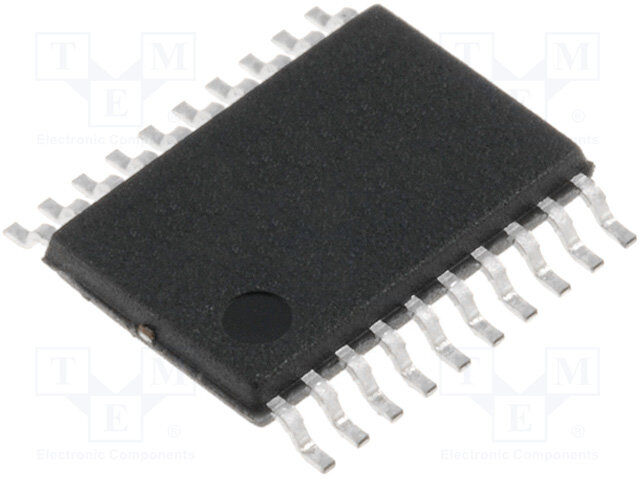
| 供应商器件封装 | 20-TSSOP |
| 其它名称 | 497-11555 |
| 其它有关文件 | http://www.st.com/web/catalog/mmc/FM141/SC1244/SS1336/LN1003/PF219710?referrer=70071840http://www.st.com/web/catalog/mmc/FM141/SC1544/SS1375/LN1042/PF219710?referrer=70071840 |
| 包装 | 管件 |
| 可编程输入/输出端数量 | 18 |
| 商标 | STMicroelectronics |
| 处理器系列 | STM8L |
| 外设 | 红外线,POR,PWM,WDT |
| 安装风格 | SMD/SMT |
| 定时器数量 | 3 Timer |
| 封装 | Tube |
| 封装/外壳 | 20-TSSOP(0.173",4.40mm 宽) |
| 封装/箱体 | TSSOP-20 |
| 工作温度 | -40°C ~ 85°C |
| 工作电源电压 | 1.65 V to 3.6 V |
| 工厂包装数量 | 74 |
| 振荡器类型 | 内部 |
| 接口类型 | I2C, SPI, USART |
| 数据RAM大小 | 1.5 kB |
| 数据Ram类型 | RAM |
| 数据Rom类型 | EEPROM |
| 数据总线宽度 | 8 bit |
| 数据转换器 | - |
| 最大工作温度 | + 85 C |
| 最大时钟频率 | 16 MHz |
| 最小工作温度 | - 40 C |
| 标准包装 | 74 |
| 核心 | STM8 |
| 核心处理器 | STM8 |
| 核心尺寸 | 8-位 |
| 片上ADC | No |
| 特色产品 | http://www.digikey.com/product-highlights/cn/zh/segger-microcontroller-systems-flasher-tools/3226 |
| 电压-电源(Vcc/Vdd) | 1.65 V ~ 3.6 V |
| 程序存储器大小 | 4 kB |
| 程序存储器类型 | Flash |
| 程序存储容量 | 4KB(4K x 8) |
| 系列 | STM8L101F2 |
| 输入/输出端数量 | 18 I/O |
| 连接性 | I²C, SPI, UART/USART |
| 速度 | 16MHz |


- 商务部:美国ITC正式对集成电路等产品启动337调查
- 曝三星4nm工艺存在良率问题 高通将骁龙8 Gen1或转产台积电
- 太阳诱电将投资9.5亿元在常州建新厂生产MLCC 预计2023年完工
- 英特尔发布欧洲新工厂建设计划 深化IDM 2.0 战略
- 台积电先进制程称霸业界 有大客户加持明年业绩稳了
- 达到5530亿美元!SIA预计今年全球半导体销售额将创下新高
- 英特尔拟将自动驾驶子公司Mobileye上市 估值或超500亿美元
- 三星加码芯片和SET,合并消费电子和移动部门,撤换高东真等 CEO
- 三星电子宣布重大人事变动 还合并消费电子和移动部门
- 海关总署:前11个月进口集成电路产品价值2.52万亿元 增长14.8%


PDF Datasheet 数据手册内容提取
STM8L101x1 STM8L101x2 STM8L101x3 8-bit ultra-low power microcontroller with up to 8 Kbytes Flash, multifunction timers, comparators, USART, SPI, I2C Datasheet - production data Features • Main microcontroller features – Supply voltage range 1.65 V to 3.6 V UFQFPN32 – Low power consumption (Halt: 0.3 µA, 5 x 5 mm UFQFPN28 LQFP32 4 x 4 mm Active-halt: 0.8 µA, Dynamic Run: 7x7 mm 150 µA/MHz) – STM8 Core with up to 16 CISC MIPS throughput UFQFPN20 TSSOP20 – Temp. range: -40 to 85 °C and 125 °C 3 x 3 mm 6.5 x 6.4 mm • Memories • Peripherals – Up to 8 Kbytes of Flash program including – Two 16-bit general purpose timers (TIM2 up to 2 Kbytes of data EEPROM and TIM3) with up and down counter and 2 – Error correction code (ECC) channels (used as IC, OC, PWM) – Flexible write and read protection modes – One 8-bit timer (TIM4) with 7-bit prescaler – In-application and in-circuit programming – Infrared remote control (IR) – Data EEPROM capability – Independent watchdog – 1.5 Kbytes of static RAM – Auto-wakeup unit • Clock management – Beeper timer with 1, 2 or 4 kHz frequencies – Internal 16 MHz RC with fast wakeup time – SPI synchronous serial interface (typ. 4 µs) – Fast I2C Multimaster/slave 400 kHz – Internal low consumption 38 kHz RC – USART with fractional baud rate generator driving both the IWDG and the AWU – 2 comparators with 4 inputs each • Reset and supply management • Development support – Ultra-low power POR/PDR – Hardware single wire interface module – Three low-power modes: Wait, Active-halt, (SWIM) for fast on-chip programming and Halt non intrusive debugging • Interrupt management – In-circuit emulation (ICE) – Nested interrupt controller with software • 96-bit unique ID priority control – Up to 29 external interrupt sources Table 1. Device summary • I/Os Reference Part numbers – Up to 30 I/Os, all mappable on external STM8L101x1 STM8L101F1 interrupt vectors – I/Os with programmable input pull-ups, high STM8L101x2 STM8L101F2, STM8L101G2 sink/source capability and one LED driver STM8L101F3, STM8L101G3, STM8L101x3 infrared output STM8L101K3 May 2017 DocID15275 Rev 16 1/88 This is information on a product in full production. www.st.com
Contents STM8L101x1 STM8L101x2 STM8L101x3 Contents 1 Introduction . . . . . . . . . . . . . . . . . . . . . . . . . . . . . . . . . . . . . . . . . . . . . . . . 8 2 Description . . . . . . . . . . . . . . . . . . . . . . . . . . . . . . . . . . . . . . . . . . . . . . . . . 9 3 Product overview . . . . . . . . . . . . . . . . . . . . . . . . . . . . . . . . . . . . . . . . . . 10 3.1 Central processing unit STM8 . . . . . . . . . . . . . . . . . . . . . . . . . . . . . . . . . .11 3.2 Development tools . . . . . . . . . . . . . . . . . . . . . . . . . . . . . . . . . . . . . . . . . . .11 3.3 Single wire data interface (SWIM) and debug module . . . . . . . . . . . . . . . .11 3.4 Interrupt controller . . . . . . . . . . . . . . . . . . . . . . . . . . . . . . . . . . . . . . . . . . .11 3.5 Memory . . . . . . . . . . . . . . . . . . . . . . . . . . . . . . . . . . . . . . . . . . . . . . . . . . 12 3.6 Low power modes . . . . . . . . . . . . . . . . . . . . . . . . . . . . . . . . . . . . . . . . . . 12 3.7 Voltage regulators . . . . . . . . . . . . . . . . . . . . . . . . . . . . . . . . . . . . . . . . . . 12 3.8 Clock control . . . . . . . . . . . . . . . . . . . . . . . . . . . . . . . . . . . . . . . . . . . . . . . 12 3.9 Independent watchdog . . . . . . . . . . . . . . . . . . . . . . . . . . . . . . . . . . . . . . . 12 3.10 Auto-wakeup counter . . . . . . . . . . . . . . . . . . . . . . . . . . . . . . . . . . . . . . . . 13 3.11 General purpose and basic timers . . . . . . . . . . . . . . . . . . . . . . . . . . . . . . 13 3.12 Beeper . . . . . . . . . . . . . . . . . . . . . . . . . . . . . . . . . . . . . . . . . . . . . . . . . . . 13 3.13 Infrared (IR) interface . . . . . . . . . . . . . . . . . . . . . . . . . . . . . . . . . . . . . . . . 13 3.14 Comparators . . . . . . . . . . . . . . . . . . . . . . . . . . . . . . . . . . . . . . . . . . . . . . . 13 3.15 USART . . . . . . . . . . . . . . . . . . . . . . . . . . . . . . . . . . . . . . . . . . . . . . . . . . . 14 3.16 SPI . . . . . . . . . . . . . . . . . . . . . . . . . . . . . . . . . . . . . . . . . . . . . . . . . . . . . . 14 3.17 I²C . . . . . . . . . . . . . . . . . . . . . . . . . . . . . . . . . . . . . . . . . . . . . . . . . . . . . . 14 4 Pin description . . . . . . . . . . . . . . . . . . . . . . . . . . . . . . . . . . . . . . . . . . . . 15 5 Memory and register map . . . . . . . . . . . . . . . . . . . . . . . . . . . . . . . . . . . . 23 6 Interrupt vector mapping . . . . . . . . . . . . . . . . . . . . . . . . . . . . . . . . . . . . 32 7 Option bytes . . . . . . . . . . . . . . . . . . . . . . . . . . . . . . . . . . . . . . . . . . . . . . 34 8 Unique ID . . . . . . . . . . . . . . . . . . . . . . . . . . . . . . . . . . . . . . . . . . . . . . . . . 36 2/88 DocID15275 Rev 16
STM8L101x1 STM8L101x2 STM8L101x3 Contents 9 Electrical parameters . . . . . . . . . . . . . . . . . . . . . . . . . . . . . . . . . . . . . . . 37 9.1 Parameter conditions . . . . . . . . . . . . . . . . . . . . . . . . . . . . . . . . . . . . . . . . 37 9.1.1 Minimum and maximum values . . . . . . . . . . . . . . . . . . . . . . . . . . . . . . . 37 9.1.2 Typical values . . . . . . . . . . . . . . . . . . . . . . . . . . . . . . . . . . . . . . . . . . . . 37 9.1.3 Typical curves . . . . . . . . . . . . . . . . . . . . . . . . . . . . . . . . . . . . . . . . . . . . 37 9.1.4 Loading capacitor . . . . . . . . . . . . . . . . . . . . . . . . . . . . . . . . . . . . . . . . . 37 9.1.5 Pin input voltage . . . . . . . . . . . . . . . . . . . . . . . . . . . . . . . . . . . . . . . . . . 38 9.2 Absolute maximum ratings . . . . . . . . . . . . . . . . . . . . . . . . . . . . . . . . . . . . 38 9.3 Operating conditions . . . . . . . . . . . . . . . . . . . . . . . . . . . . . . . . . . . . . . . . 40 9.3.1 General operating conditions . . . . . . . . . . . . . . . . . . . . . . . . . . . . . . . . . 40 9.3.2 Power-up / power-down operating conditions . . . . . . . . . . . . . . . . . . . . 41 9.3.3 Supply current characteristics . . . . . . . . . . . . . . . . . . . . . . . . . . . . . . . . 41 9.3.4 Clock and timing characteristics . . . . . . . . . . . . . . . . . . . . . . . . . . . . . . 45 9.3.5 Memory characteristics . . . . . . . . . . . . . . . . . . . . . . . . . . . . . . . . . . . . . 47 9.3.6 I/O port pin characteristics . . . . . . . . . . . . . . . . . . . . . . . . . . . . . . . . . . . 48 9.3.7 Communication interfaces . . . . . . . . . . . . . . . . . . . . . . . . . . . . . . . . . . . 55 9.3.8 Comparator characteristics . . . . . . . . . . . . . . . . . . . . . . . . . . . . . . . . . . 59 9.3.9 EMC characteristics . . . . . . . . . . . . . . . . . . . . . . . . . . . . . . . . . . . . . . . . 60 9.4 Thermal characteristics . . . . . . . . . . . . . . . . . . . . . . . . . . . . . . . . . . . . . . 62 10 Package information . . . . . . . . . . . . . . . . . . . . . . . . . . . . . . . . . . . . . . . . 64 10.1 UFQFPN32 package information . . . . . . . . . . . . . . . . . . . . . . . . . . . . . . . 64 10.2 LQFP32 package information . . . . . . . . . . . . . . . . . . . . . . . . . . . . . . . . . . 67 10.3 UFQFPN28 package information . . . . . . . . . . . . . . . . . . . . . . . . . . . . . . . 70 10.4 UFQFPN20 package information . . . . . . . . . . . . . . . . . . . . . . . . . . . . . . . 73 10.5 TSSOP20 package information . . . . . . . . . . . . . . . . . . . . . . . . . . . . . . . . 76 11 Device ordering information . . . . . . . . . . . . . . . . . . . . . . . . . . . . . . . . . 79 12 STM8 development tools . . . . . . . . . . . . . . . . . . . . . . . . . . . . . . . . . . . . 80 12.1 Emulation and in-circuit debugging tools . . . . . . . . . . . . . . . . . . . . . . . . . 80 12.2 Software tools . . . . . . . . . . . . . . . . . . . . . . . . . . . . . . . . . . . . . . . . . . . . . . 81 12.2.1 STM8 toolset . . . . . . . . . . . . . . . . . . . . . . . . . . . . . . . . . . . . . . . . . . . . . 81 12.2.2 C and assembly toolchains . . . . . . . . . . . . . . . . . . . . . . . . . . . . . . . . . . 81 12.3 Programming tools . . . . . . . . . . . . . . . . . . . . . . . . . . . . . . . . . . . . . . . . . . 81 DocID15275 Rev 16 3/88 4
Contents STM8L101x1 STM8L101x2 STM8L101x3 13 Revision history . . . . . . . . . . . . . . . . . . . . . . . . . . . . . . . . . . . . . . . . . . . 82 4/88 DocID15275 Rev 16
STM8L101x1 STM8L101x2 STM8L101x3 List of tables List of tables Table 1. Device summary. . . . . . . . . . . . . . . . . . . . . . . . . . . . . . . . . . . . . . . . . . . . . . . . . . . . . . . . . . 1 Table 2. STM8L101xx device feature summary. . . . . . . . . . . . . . . . . . . . . . . . . . . . . . . . . . . . . . . . . 9 Table 3. Legend/abbreviation for table 4 . . . . . . . . . . . . . . . . . . . . . . . . . . . . . . . . . . . . . . . . . . . . . 20 Table 4. STM8L101xx pin description . . . . . . . . . . . . . . . . . . . . . . . . . . . . . . . . . . . . . . . . . . . . . . . 20 Table 5. Flash and RAM boundary addresses. . . . . . . . . . . . . . . . . . . . . . . . . . . . . . . . . . . . . . . . . 24 Table 6. I/O Port hardware register map . . . . . . . . . . . . . . . . . . . . . . . . . . . . . . . . . . . . . . . . . . . . . 24 Table 7. General hardware register map . . . . . . . . . . . . . . . . . . . . . . . . . . . . . . . . . . . . . . . . . . . . . 25 Table 8. CPU/SWIM/debug module/interrupt controller registers. . . . . . . . . . . . . . . . . . . . . . . . . . . 30 Table 9. Interrupt mapping . . . . . . . . . . . . . . . . . . . . . . . . . . . . . . . . . . . . . . . . . . . . . . . . . . . . . . . . 32 Table 10. Option bytes . . . . . . . . . . . . . . . . . . . . . . . . . . . . . . . . . . . . . . . . . . . . . . . . . . . . . . . . . . . . 34 Table 11. Option byte description. . . . . . . . . . . . . . . . . . . . . . . . . . . . . . . . . . . . . . . . . . . . . . . . . . . . 34 Table 12. Unique ID registers (96 bits). . . . . . . . . . . . . . . . . . . . . . . . . . . . . . . . . . . . . . . . . . . . . . . . 36 Table 13. Voltage characteristics . . . . . . . . . . . . . . . . . . . . . . . . . . . . . . . . . . . . . . . . . . . . . . . . . . . . 38 Table 14. Current characteristics . . . . . . . . . . . . . . . . . . . . . . . . . . . . . . . . . . . . . . . . . . . . . . . . . . . . 39 Table 15. Thermal characteristics. . . . . . . . . . . . . . . . . . . . . . . . . . . . . . . . . . . . . . . . . . . . . . . . . . . . 39 Table 16. General operating conditions . . . . . . . . . . . . . . . . . . . . . . . . . . . . . . . . . . . . . . . . . . . . . . . 40 Table 17. Operating conditions at power-up / power-down . . . . . . . . . . . . . . . . . . . . . . . . . . . . . . . . 41 Table 18. Total current consumption in Run mode . . . . . . . . . . . . . . . . . . . . . . . . . . . . . . . . . . . . . . 42 Table 19. Total current consumption in Wait mode . . . . . . . . . . . . . . . . . . . . . . . . . . . . . . . . . . . . . . 43 Table 20. Total current consumption and timing in Halt and Active-halt mode at VDD = 1.65 V to 3.6 V . . . . . . . . . . . . . . . . . . . . . . . . . . . . . . . . . . . . . . . . . . . . . . . . . . . . 44 Table 21. Peripheral current consumption . . . . . . . . . . . . . . . . . . . . . . . . . . . . . . . . . . . . . . . . . . . . . 45 Table 22. HSI oscillator characteristics . . . . . . . . . . . . . . . . . . . . . . . . . . . . . . . . . . . . . . . . . . . . . . . 45 Table 23. LSI oscillator characteristics . . . . . . . . . . . . . . . . . . . . . . . . . . . . . . . . . . . . . . . . . . . . . . . 47 Table 24. RAM and hardware registers . . . . . . . . . . . . . . . . . . . . . . . . . . . . . . . . . . . . . . . . . . . . . . . 47 Table 25. Flash program memory. . . . . . . . . . . . . . . . . . . . . . . . . . . . . . . . . . . . . . . . . . . . . . . . . . . . 47 Table 26. I/O static characteristics . . . . . . . . . . . . . . . . . . . . . . . . . . . . . . . . . . . . . . . . . . . . . . . . . . . 48 Table 27. Output driving current (High sink ports) . . . . . . . . . . . . . . . . . . . . . . . . . . . . . . . . . . . . . . . 51 Table 28. Output driving current (true open drain ports). . . . . . . . . . . . . . . . . . . . . . . . . . . . . . . . . . . 51 Table 29. Output driving current (PA0 with high sink LED driver capability). . . . . . . . . . . . . . . . . . . . 51 Table 30. NRST pin characteristics . . . . . . . . . . . . . . . . . . . . . . . . . . . . . . . . . . . . . . . . . . . . . . . . . . 53 Table 31. SPI characteristics . . . . . . . . . . . . . . . . . . . . . . . . . . . . . . . . . . . . . . . . . . . . . . . . . . . . . . . 55 Table 32. I2C characteristics . . . . . . . . . . . . . . . . . . . . . . . . . . . . . . . . . . . . . . . . . . . . . . . . . . . . . . . 58 Table 33. Comparator characteristics. . . . . . . . . . . . . . . . . . . . . . . . . . . . . . . . . . . . . . . . . . . . . . . . . 59 Table 34. EMS data . . . . . . . . . . . . . . . . . . . . . . . . . . . . . . . . . . . . . . . . . . . . . . . . . . . . . . . . . . . . . . 60 Table 35. EMI data . . . . . . . . . . . . . . . . . . . . . . . . . . . . . . . . . . . . . . . . . . . . . . . . . . . . . . . . . . . . . . 61 Table 36. ESD absolute maximum ratings. . . . . . . . . . . . . . . . . . . . . . . . . . . . . . . . . . . . . . . . . . . . . 61 Table 37. Electrical sensitivities . . . . . . . . . . . . . . . . . . . . . . . . . . . . . . . . . . . . . . . . . . . . . . . . . . . . . 62 Table 38. Thermal characteristics. . . . . . . . . . . . . . . . . . . . . . . . . . . . . . . . . . . . . . . . . . . . . . . . . . . . 63 Table 39. UFQFPN32 - 32-lead ultra thin fine pitch quad flat no-lead package (5 x 5), package mechanical data. . . . . . . . . . . . . . . . . . . . . . . . . . . . . . . . . . . . . . . . . . . . . . . . . . 65 Table 40. LQFP32- 32-pin low profile quad flat package (7x7), package mechanical data . . . . . . . . 68 Table 41. UFQFPN28 - 28-lead ultra thin fine pitch quad flat no-lead package (4 x 4), package mechanical data. . . . . . . . . . . . . . . . . . . . . . . . . . . . . . . . . . . . . . . . . . . . . . . . . . 71 Table 42. UFQFPN20 - 20-lead, 3x3 mm, 0.5 mm pitch, ultra thin fine pitch quad flat package mechanical data. . . . . . . . . . . . . . . . . . . . . . . . . . . . . . . . . . . . . . . . . . . . . . . . . . 74 Table 43. TSSOP20 - 20-lead thin shrink small package mechanical data . . . . . . . . . . . . . . . . . . . . 76 Table 44. Document revision history . . . . . . . . . . . . . . . . . . . . . . . . . . . . . . . . . . . . . . . . . . . . . . . . . 82 DocID15275 Rev 16 5/88 5
List of figures STM8L101x1 STM8L101x2 STM8L101x3 List of figures Figure 1. STM8L101xx device block diagram . . . . . . . . . . . . . . . . . . . . . . . . . . . . . . . . . . . . . . . . . . 10 Figure 2. Standard 20-pin UFQFPN package pinout. . . . . . . . . . . . . . . . . . . . . . . . . . . . . . . . . . . . . 15 Figure 3. 20-pin UFQFPN package pinout for STM8L101F1U6ATR, STM8L101F2U6ATR and STM8L101F3U6ATR part numbers. . . . . . . . . . . . . . . . . . . . . . 16 Figure 4. 20-pin TSSOP package pinout. . . . . . . . . . . . . . . . . . . . . . . . . . . . . . . . . . . . . . . . . . . . . . 17 Figure 5. Standard 28-pin UFQFPN package pinout. . . . . . . . . . . . . . . . . . . . . . . . . . . . . . . . . . . . . 17 Figure 6. 28-pin UFQFPN package pinout for STM8L101G3U6ATR and STM8L101G2U6ATR part numbers. . . . . . . . . . . . . . . . . . . . . . . . . . . . . . . . . . . . . . . . . . 18 Figure 7. 32-pin package pinout . . . . . . . . . . . . . . . . . . . . . . . . . . . . . . . . . . . . . . . . . . . . . . . . . . . . 19 Figure 8. Memory map. . . . . . . . . . . . . . . . . . . . . . . . . . . . . . . . . . . . . . . . . . . . . . . . . . . . . . . . . . . . 23 Figure 9. Pin loading conditions. . . . . . . . . . . . . . . . . . . . . . . . . . . . . . . . . . . . . . . . . . . . . . . . . . . . . 37 Figure 10. Pin input voltage. . . . . . . . . . . . . . . . . . . . . . . . . . . . . . . . . . . . . . . . . . . . . . . . . . . . . . . . . 38 Figure 11. IDD(RUN) vs. VDD, fCPU = 2 MHz . . . . . . . . . . . . . . . . . . . . . . . . . . . . . . . . . . . . . . . . . . 42 Figure 12. IDD(RUN) vs. VDD, fCPU = 16 MHz . . . . . . . . . . . . . . . . . . . . . . . . . . . . . . . . . . . . . . . . . 42 Figure 13. IDD(WAIT) vs. VDD, fCPU = 2 MHz. . . . . . . . . . . . . . . . . . . . . . . . . . . . . . . . . . . . . . . . . . 43 Figure 14. IDD(WAIT) vs. VDD, fCPU = 16 MHz. . . . . . . . . . . . . . . . . . . . . . . . . . . . . . . . . . . . . . . . . 43 Figure 15. Typ. IDD(Halt) vs. VDD, fCPU = 2 MHz and 16 MHz . . . . . . . . . . . . . . . . . . . . . . . . . . . . 44 Figure 16. Typical HSI frequency vs. V . . . . . . . . . . . . . . . . . . . . . . . . . . . . . . . . . . . . . . . . . . . . . . 46 DD Figure 17. Typical HSI accuracy vs. temperature, V = 3 V . . . . . . . . . . . . . . . . . . . . . . . . . . . . . . . 46 DD Figure 18. Typical HSI accuracy vs. temperature, VDD = 1.65 V to 3.6 V. . . . . . . . . . . . . . . . . . . . . . 46 Figure 19. Typical LSI RC frequency vs. VDD. . . . . . . . . . . . . . . . . . . . . . . . . . . . . . . . . . . . . . . . . . . 47 Figure 20. Typical VIL and VIH vs. VDD (High sink I/Os) . . . . . . . . . . . . . . . . . . . . . . . . . . . . . . . . . . 49 Figure 21. Typical VIL and VIH vs. VDD (true open drain I/Os). . . . . . . . . . . . . . . . . . . . . . . . . . . . . . 50 Figure 22. Typical pull-up resistance R vs. V with VIN=VSS. . . . . . . . . . . . . . . . . . . . . . . . . . . . 50 PU DD Figure 23. Typical pull-up current I vs. V with VIN=VSS . . . . . . . . . . . . . . . . . . . . . . . . . . . . . . . 50 PU DD Figure 24. Typ. VOL at VDD = 3.0 V (High sink ports) . . . . . . . . . . . . . . . . . . . . . . . . . . . . . . . . . . . . 52 Figure 25. Typ. VOL at VDD = 1.8 V (High sink ports) . . . . . . . . . . . . . . . . . . . . . . . . . . . . . . . . . . . . 52 Figure 26. Typ. VOL at VDD = 3.0 V (true open drain ports). . . . . . . . . . . . . . . . . . . . . . . . . . . . . . . . 52 Figure 27. Typ. VOL at VDD = 1.8 V (true open drain ports). . . . . . . . . . . . . . . . . . . . . . . . . . . . . . . . 52 Figure 28. Typ. VDD - VOH at VDD = 3.0 V (High sink ports). . . . . . . . . . . . . . . . . . . . . . . . . . . . . . . 52 Figure 29. Typ. VDD - VOH at VDD = 1.8 V (High sink ports). . . . . . . . . . . . . . . . . . . . . . . . . . . . . . . 52 Figure 30. Typical NRST pull-up resistance R vs. V . . . . . . . . . . . . . . . . . . . . . . . . . . . . . . . . . . 53 PU DD Figure 31. Typical NRST pull-up current I vs. V . . . . . . . . . . . . . . . . . . . . . . . . . . . . . . . . . . . . . . 54 pu DD Figure 32. Recommended NRST pin configuration. . . . . . . . . . . . . . . . . . . . . . . . . . . . . . . . . . . . . . . 54 Figure 33. SPI timing diagram - slave mode and CPHA = 0 . . . . . . . . . . . . . . . . . . . . . . . . . . . . . . . . 56 Figure 34. SPI timing diagram - slave mode and CPHA = 1(1) . . . . . . . . . . . . . . . . . . . . . . . . . . . . . . 56 Figure 35. SPI timing diagram - master mode(1) . . . . . . . . . . . . . . . . . . . . . . . . . . . . . . . . . . . . . . . . . 57 Figure 36. Typical application with I2C bus and timing diagram 1) . . . . . . . . . . . . . . . . . . . . . . . . . . . 59 Figure 37. UFQFPN32 - 32-lead ultra thin fine pitch quad flat no-lead package outline (5 x 5). . . . . . 64 Figure 38. UFQFPN32 recommended footprint. . . . . . . . . . . . . . . . . . . . . . . . . . . . . . . . . . . . . . . . . . 65 Figure 39. UFQFPN32 marking example (package top view) . . . . . . . . . . . . . . . . . . . . . . . . . . . . . . . 66 Figure 40. LQFP32 - 32-pin low profile quad flat package outline (7 x 7) . . . . . . . . . . . . . . . . . . . . . . 67 Figure 41. LQFP32 recommended footprint . . . . . . . . . . . . . . . . . . . . . . . . . . . . . . . . . . . . . . . . . . . . 69 Figure 42. LQFP32 marking example (package top view). . . . . . . . . . . . . . . . . . . . . . . . . . . . . . . . . . 69 Figure 43. UFQFPN28 - 28-lead ultra thin fine pitch quad flat no-lead package outline (4 x 4 mm) . . 70 Figure 44. UFQFPN28 recommended footprint. . . . . . . . . . . . . . . . . . . . . . . . . . . . . . . . . . . . . . . . . . 71 Figure 45. UFQFPN28 marking example (package top view) . . . . . . . . . . . . . . . . . . . . . . . . . . . . . . . 72 Figure 46. UFQFPN20 - 20-lead, 3x3 mm, 0.5 mm pitch, ultra thin fine pitch quad flat 6/88 DocID15275 Rev 16
STM8L101x1 STM8L101x2 STM8L101x3 List of figures package outline. . . . . . . . . . . . . . . . . . . . . . . . . . . . . . . . . . . . . . . . . . . . . . . . . . . . . . . . . . 73 Figure 47. UFQFPN20 - 20-lead, 3x3 mm, 0.5 mm pitch, ultra thin fine pitch quad flat package recommended footprint . . . . . . . . . . . . . . . . . . . . . . . . . . . . . . . . . . . . . . . . . . . . 74 Figure 48. UFQFPN20 marking example (package top view) . . . . . . . . . . . . . . . . . . . . . . . . . . . . . . . 75 Figure 49. TSSOP20 - 20-lead thin shrink small package outline . . . . . . . . . . . . . . . . . . . . . . . . . . . 76 Figure 50. TSSOP20 recommended footprint . . . . . . . . . . . . . . . . . . . . . . . . . . . . . . . . . . . . . . . . . . . 77 Figure 51. TSSOP20 marking example (package top view) . . . . . . . . . . . . . . . . . . . . . . . . . . . . . . . . 78 Figure 52. STM8L101xx ordering information scheme . . . . . . . . . . . . . . . . . . . . . . . . . . . . . . . . . . . . 79 DocID15275 Rev 16 7/88 7
Introduction STM8L101x1 STM8L101x2 STM8L101x3 1 Introduction This datasheet provides the STM8L101x1 STM8L101x2 STM8L101x3 pinout, ordering information, mechanical and electrical device characteristics. For complete information on the STM8L101x1 STM8L101x2 STM8L101x3 microcontroller memory, registers and peripherals, please refer to the STM8L reference manual. The STM8L101x1 STM8L101x2 STM8L101x3devices are members of the STM8L low- power 8-bit family. They are referred to as low-density devices in the STM8L101x1 STM8L101x2 STM8L101x3 microcontroller family reference manual (RM0013) and in the STM8L Flash programming manual (PM0054). All devices of the SM8L product line provide the following benefits: • Reduced system cost – Up to 8 Kbytes of low-density embedded Flash program memory including up to 2 Kbytes of data EEPROM – High system integration level with internal clock oscillators and watchdogs. – Smaller battery and cheaper power supplies. • Low power consumption and advanced features – Up to 16 MIPS at 16 MHz CPU clock frequency – Less than 150 µA/MH, 0.8 µA in Active-halt mode, and 0.3 µA in Halt mode – Clock gated system and optimized power management • Short development cycles – Application scalability across a common family product architecture with compatible pinout, memory map and modular peripherals. – Full documentation and a wide choice of development tools • Product longevity – Advanced core and peripherals made in a state-of-the art technology – Product family operating from 1.65 V to 3.6 V supply. 8/88 DocID15275 Rev 16
STM8L101x1 STM8L101x2 STM8L101x3 Description 2 Description The STM8L101x1 STM8L101x2 STM8L101x3 low-power family features the enhanced STM8 CPU core providing increased processing power (up to 16 MIPS at 16 MHz) while maintaining the advantages of a CISC architecture with improved code density, a 24-bit linear addressing space and an optimized architecture for low power operations. The family includes an integrated debug module with a hardware interface (SWIM) which allows non-intrusive in-application debugging and ultrafast Flash programming. All STM8L101xx microcontrollers feature low power low-voltage single-supply program Flash memory. The 8-Kbyte devices embed data EEPROM. The STM8L101xx low power family is based on a generic set of state-of-the-art peripherals. The modular design of the peripheral set allows the same peripherals to be found in different ST microcontroller families including 32-bit families. This makes any transition to a different family very easy, and simplified even more by the use of a common set of development tools. All STM8L low power products are based on the same architecture with the same memory mapping and a coherent pinout. Table 2. STM8L101xx device feature summary Features STM8L101xx 8 Kbytes of Flash program 2 Kbytes of Flash program 4 Kbytes of Flash program Flash memory including up to memory memory 2 Kbytes of Data EEPROM RAM 1.5 Kbytes Independent watchdog (IWDG), Auto-wakeup unit (AWU), Beep, Serial peripheral interface (SPI), Inter-integrated circuit (I²C), Peripheral functions Universal synchronous / asynchronous receiver / transmitter (USART), 2 comparators, Infrared (IR) interface Timers Two 16-bit timers, one 8-bit timer Operating voltage 1.65 to 3.6 V -40 to +85 °C or Operating temperature -40 to +85 °C -40 to +125 °C UFQFPN28 4x4 UFQFPN28 4x 4 UFQFPN20 3x3 Packages UFQFPN20 3x3 UFQFPN20 3x3 UFQFPN32 TSSOP20 4.4 x 6.4 LQFP32 DocID15275 Rev 16 9/88 22
Product overview STM8L101x1 STM8L101x2 STM8L101x3 3 Product overview Figure 1. STM8L101xx device block diagram (cid:35)(cid:3)(cid:57)(cid:39)(cid:39) (cid:20)(cid:25)(cid:3)(cid:48)(cid:43)(cid:93)(cid:3)(cid:76)(cid:81)(cid:87)(cid:3)(cid:53)(cid:38)(cid:3)(cid:3) (cid:70)(cid:82)(cid:38)(cid:81)(cid:87)(cid:79)(cid:85)(cid:82)(cid:82)(cid:70)(cid:79)(cid:78)(cid:79)(cid:72)(cid:85) (cid:57)(cid:39)(cid:39)(cid:20)(cid:27) (cid:57)(cid:82)(cid:51)(cid:79)(cid:82)(cid:87)(cid:17)(cid:90)(cid:3)(cid:85)(cid:72)(cid:72)(cid:74)(cid:85)(cid:17) (cid:57)(cid:57)(cid:54)(cid:39)(cid:54)(cid:39)(cid:3)(cid:32)(cid:3)(cid:20)(cid:17)(cid:25)(cid:24)(cid:57)(cid:3)(cid:87)(cid:82)(cid:3)(cid:22)(cid:17)(cid:25)(cid:57) (cid:22)(cid:27)(cid:3)(cid:78)(cid:43)(cid:93)(cid:3)(cid:76)(cid:81)(cid:87)(cid:3)(cid:53)(cid:38)(cid:3)(cid:3) (cid:38)(cid:79)(cid:82)(cid:70)(cid:78)(cid:86) (cid:87)(cid:82)(cid:3)(cid:70)(cid:82)(cid:85)(cid:72)(cid:3)(cid:68)(cid:81)(cid:71) (cid:53)(cid:72)(cid:86)(cid:72)(cid:87) (cid:49)(cid:53)(cid:54)(cid:55) (cid:83)(cid:72)(cid:85)(cid:76)(cid:83)(cid:75)(cid:72)(cid:85)(cid:68)(cid:79)(cid:86) (cid:51)(cid:50)(cid:53)(cid:18)(cid:51)(cid:39)(cid:53) (cid:54)(cid:55)(cid:48)(cid:27) (cid:38)(cid:82)(cid:85)(cid:72) (cid:56)(cid:83)(cid:3)(cid:87)(cid:82)(cid:3)(cid:27)(cid:3)(cid:46)(cid:69)(cid:92)(cid:87)(cid:72)(cid:86) (cid:88)(cid:83)(cid:3)(cid:87)(cid:82)(cid:3)(cid:20)(cid:25)(cid:3)(cid:48)(cid:43)(cid:93) (cid:41)(cid:79)(cid:68)(cid:86)(cid:75)(cid:3)(cid:80)(cid:72)(cid:80)(cid:82)(cid:85)(cid:92) (cid:11)(cid:76)(cid:81)(cid:70)(cid:79)(cid:88)(cid:71)(cid:76)(cid:81)(cid:74) (cid:88)(cid:83)(cid:3)(cid:87)(cid:82)(cid:3)(cid:21)(cid:3)(cid:46)(cid:69)(cid:92)(cid:87)(cid:72)(cid:86) (cid:71)(cid:68)(cid:87)(cid:68)(cid:3)(cid:40)(cid:40)(cid:51)(cid:53)(cid:50)(cid:48)(cid:12) (cid:49)(cid:72)(cid:86)(cid:87)(cid:72)(cid:71)(cid:3)(cid:76)(cid:81)(cid:87)(cid:72)(cid:85)(cid:85)(cid:88)(cid:83)(cid:87) (cid:70)(cid:82)(cid:81)(cid:87)(cid:85)(cid:82)(cid:79)(cid:79)(cid:72)(cid:85) (cid:20)(cid:17)(cid:24)(cid:3)(cid:46)(cid:69)(cid:92)(cid:87)(cid:72)(cid:86) (cid:88)(cid:83)(cid:3)(cid:87)(cid:82)(cid:3)(cid:21)(cid:28)(cid:3)(cid:72)(cid:91)(cid:87)(cid:72)(cid:85)(cid:81)(cid:68)(cid:79)(cid:3)(cid:3) (cid:54)(cid:53)(cid:36)(cid:48) (cid:76)(cid:81)(cid:87)(cid:72)(cid:85)(cid:85)(cid:88)(cid:83)(cid:87)(cid:86) (cid:54)(cid:58)(cid:44)(cid:48) (cid:39)(cid:72)(cid:69)(cid:11)(cid:88)(cid:54)(cid:74)(cid:58)(cid:3)(cid:80)(cid:44)(cid:48)(cid:82)(cid:71)(cid:12)(cid:88)(cid:79)(cid:72) (cid:36)(cid:71)(cid:71) (cid:56)(cid:54)(cid:36)(cid:53)(cid:55) (cid:53)(cid:59)(cid:15)(cid:3)(cid:55)(cid:59)(cid:15)(cid:3)(cid:38)(cid:46) (cid:85)(cid:72)(cid:86)(cid:86)(cid:3)(cid:68) (cid:80)(cid:88)(cid:79)(cid:87)(cid:76)(cid:44)(cid:80)(cid:240)(cid:38)(cid:68)(cid:20)(cid:86)(cid:87)(cid:72)(cid:85) (cid:54)(cid:39)(cid:36)(cid:15)(cid:3)(cid:54)(cid:38)(cid:47) (cid:44)(cid:53)(cid:66)(cid:55)(cid:44)(cid:48) (cid:44)(cid:81)(cid:73)(cid:85)(cid:68)(cid:85)(cid:72)(cid:71)(cid:3)(cid:76)(cid:81)(cid:87)(cid:72)(cid:85)(cid:73)(cid:68)(cid:70)(cid:72) (cid:81)(cid:71) (cid:3)(cid:71)(cid:68)(cid:87)(cid:68) (cid:54)(cid:51)(cid:44) (cid:48)(cid:54)(cid:38)(cid:50)(cid:46)(cid:54)(cid:15)(cid:44)(cid:3)(cid:15)(cid:49)(cid:3)(cid:48)(cid:54)(cid:44)(cid:54)(cid:54)(cid:50)(cid:15)(cid:3)(cid:3) (cid:51)(cid:36)(cid:62)(cid:25)(cid:29)(cid:19)(cid:64) (cid:51)(cid:82)(cid:85)(cid:87)(cid:3)(cid:36) (cid:3)(cid:69)(cid:88)(cid:86) (cid:20)(cid:25)(cid:16)(cid:69)(cid:76)(cid:87)(cid:3)(cid:55)(cid:76)(cid:80)(cid:72)(cid:85)(cid:3)(cid:21) (cid:55)(cid:44)(cid:48)(cid:21)(cid:66)(cid:38)(cid:43)(cid:62)(cid:21)(cid:29)(cid:20)(cid:64) (cid:51)(cid:37)(cid:62)(cid:26)(cid:29)(cid:19)(cid:64) (cid:51)(cid:82)(cid:85)(cid:87)(cid:3)(cid:37) (cid:55)(cid:44)(cid:48)(cid:21)(cid:66)(cid:55)(cid:53)(cid:44)(cid:42) (cid:51)(cid:38)(cid:62)(cid:25)(cid:29)(cid:19)(cid:64) (cid:51)(cid:82)(cid:85)(cid:87)(cid:3)(cid:38) (cid:20)(cid:25)(cid:16)(cid:69)(cid:76)(cid:87)(cid:3)(cid:55)(cid:76)(cid:80)(cid:72)(cid:85)(cid:3)(cid:22) (cid:55)(cid:55)(cid:44)(cid:44)(cid:48)(cid:48)(cid:22)(cid:22)(cid:66)(cid:66)(cid:38)(cid:55)(cid:53)(cid:43)(cid:44)(cid:62)(cid:42)(cid:21)(cid:29)(cid:20)(cid:64) (cid:51)(cid:39)(cid:62)(cid:26)(cid:29)(cid:19)(cid:64) (cid:51)(cid:82)(cid:85)(cid:87)(cid:3)(cid:39) (cid:27)(cid:16)(cid:69)(cid:76)(cid:87)(cid:3)(cid:55)(cid:76)(cid:80)(cid:72)(cid:85)(cid:3)(cid:23) (cid:38)(cid:50)(cid:48)(cid:51)(cid:20)(cid:66)(cid:38)(cid:43)(cid:62)(cid:23)(cid:29)(cid:20)(cid:64) (cid:38)(cid:50)(cid:48)(cid:51)(cid:20) (cid:44)(cid:58)(cid:39)(cid:42)(cid:3)(cid:3) (cid:38)(cid:50)(cid:48)(cid:51)(cid:66)(cid:53)(cid:40)(cid:41) (cid:36)(cid:58)(cid:56) (cid:38)(cid:50)(cid:48)(cid:51)(cid:21)(cid:66)(cid:38)(cid:43)(cid:62)(cid:23)(cid:29)(cid:20)(cid:64) (cid:38)(cid:50)(cid:48)(cid:51)(cid:21) (cid:37)(cid:72)(cid:72)(cid:83)(cid:72)(cid:85) (cid:37)(cid:40)(cid:40)(cid:51) (cid:48)(cid:54)(cid:22)(cid:21)(cid:25)(cid:20)(cid:19)(cid:57)(cid:20) Legend: AWU: Auto-wakeup unit Int. RC: internal RC oscillator I²C: Inter-integrated circuit multimaster interface POR/PDR: Power on reset / power down reset SPI: Serial peripheral interface SWIM: Single wire interface module USART: Universal synchronous / asynchronous receiver / transmitter IWDG: Independent watchdog 10/88 DocID15275 Rev 16
STM8L101x1 STM8L101x2 STM8L101x3 Product overview 3.1 Central processing unit STM8 The 8-bit STM8 core is designed for code efficiency and performance. It features 21 internal registers, 20 addressing modes including indexed, indirect and relative addressing, and 80 instructions. 3.2 Development tools Development tools for the STM8 microcontrollers include: • The STice emulation system offering tracing and code profiling • The STVD high-level language debugger including C compiler, assembler and integrated development environment • The STVP Flash programming software The STM8 also comes with starter kits, evaluation boards and low-cost in-circuit debugging/programming tools. 3.3 Single wire data interface (SWIM) and debug module The debug module with its single wire data interface (SWIM) permits non-intrusive real-time in-circuit debugging and fast memory programming. The Single wire interface is used for direct access to the debugging module and memory programming. The interface can be activated in all device operation modes. The non-intrusive debugging module features a performance close to a full-featured emulator. Beside memory and peripherals, also CPU operation can be monitored in real- time by means of shadow registers. 3.4 Interrupt controller The STM8L101xx features a nested vectored interrupt controller: • Nested interrupts with 3 software priority levels • 26 interrupt vectors with hardware priority • Up to 29 external interrupt sources on 10 vectors • Trap and reset interrupts. DocID15275 Rev 16 11/88 22
Product overview STM8L101x1 STM8L101x2 STM8L101x3 3.5 Memory The STM8L101xx devices have the following main features: • 1.5 Kbytes of RAM • The EEPROM is divided into two memory arrays (see the STM8L reference manual for details on the memory mapping): – Up to 8 Kbytes of low-density embedded Flash program including up to 2 Kbytes of data EEPROM. Data EEPROM and Flash program areas can be write protected independently by using the memory access security mechanism (MASS). – 64 option bytes (one block) of which 5 bytes are already used for the device. Error correction code is implemented on the EEPROM. 3.6 Low power modes To minimize power consumption, the product features three low power modes: • Wait mode: CPU clock stopped, selected peripherals at full clock speed. • Active-halt mode: CPU and peripheral clocks are stopped. The programmable wakeup time is controlled by the AWU unit. • Halt mode: CPU and peripheral clocks are stopped, the device remains powered on. The RAM content is preserved. Wakeup is triggered by an external interrupt. 3.7 Voltage regulators The STM8L101xx embeds an internal voltage regulator for generating the 1.8 V power supply for the core and peripherals. This regulator has two different modes: main voltage regulator mode (MVR) and low power voltage regulator mode (LPVR). When entering Halt or Active-halt modes, the system automatically switches from the MVR to the LPVR in order to reduce current consumption. 3.8 Clock control The STM8L101xx embeds a robust clock controller. It is used to distribute the system clock to the core and the peripherals and to manage clock gating for low power modes. This system clock is a 16-MHz High Speed Internal RC oscillator (HSI RC), followed by a programmable prescaler. In addition, a 38 kHz low speed internal RC oscillator is used by the independent watchdog (IWDG) and Auto-wakeup unit (AWU). 3.9 Independent watchdog The independent watchdog (IWDG) peripheral can be used to resolve processor malfunctions due to hardware or software failures. It is clocked by the 38 kHz LSI internal RC clock source, and thus stays active even in case of a CPU clock failure. 12/88 DocID15275 Rev 16
STM8L101x1 STM8L101x2 STM8L101x3 Product overview 3.10 Auto-wakeup counter The auto-wakeup (AWU) counter is used to wakeup the device from Active-halt mode. 3.11 General purpose and basic timers STM8L101xx devices contain two 16-bit general purpose timers (TIM2 and TIM3) and one 8-bit basic timer (TIM4). 16-bit general purpose timers The 16-bit timers consist of 16-bit up/down auto-reload counters driven by a programmable prescaler. They perform a wide range of functions, including: • Time base generation • Measuring the pulse lengths of input signals (input capture) • Generating output waveforms (output compare, PWM and One pulse mode) • Interrupt capability on various events (capture, compare, overflow, break, trigger) 8-bit basic timer The 8-bit timer consists of an 8-bit up auto-reload counter driven by a programmable prescaler. It can be used for timebase generation with interrupt generation on timer overflow. 3.12 Beeper The STM8L101xx devices include a beeper function used to generate a beep signal in the range of 1, 2 or 4 kHz when the LSI clock is operating at a frequency of 38 kHz. 3.13 Infrared (IR) interface The STM8L101xx devices contain an infrared interface which can be used with an IR LED for remote control functions. Two timer output compare channels are used to generate the infrared remote control signals. 3.14 Comparators The STM8L101xx features two zero-crossing comparators (COMP1 and COMP2) sharing the same current bias and voltage reference. The voltage reference can be internal (comparison with ground) or external (comparison to a reference pin voltage). Each comparator is connected to 4 channels, which can be used to generate interrupt, timer input capture or timer break. Their polarity can be inverted. DocID15275 Rev 16 13/88 22
Product overview STM8L101x1 STM8L101x2 STM8L101x3 3.15 USART The USART interface (USART) allows full duplex, asynchronous communications with external devices requiring an industry standard NRZ asynchronous serial data format. It offers a very wide range of baud rates. 3.16 SPI The serial peripheral interface (SPI) provides half/ full duplex synchronous serial communication with external devices. It can be configured as the master and in this case it provides the communication clock (SCK) to the external slave device. The interface can also operate in multi-master configuration. 3.17 I²C The inter-integrated circuit (I2C) bus interface is designed to serve as an interface between the microcontroller and the serial I2C bus. It provides multi-master capability, and controls all I²C bus-specific sequencing, protocol, arbitration and timing. It manages standard and fast speed modes. 14/88 DocID15275 Rev 16
STM8L101x1 STM8L101x2 STM8L101x3 Pin description 4 Pin description Figure 2. Standard 20-pin UFQFPN package pinout (cid:54)(cid:12)(cid:54)(cid:12) (cid:54)(cid:12) (cid:54)(cid:12) (cid:43)(cid:43) (cid:43) (cid:43) (cid:19)(cid:3)(cid:11)(cid:23)(cid:3)(cid:11) (cid:22)(cid:3)(cid:11) (cid:21)(cid:3)(cid:11)(cid:20) (cid:36)(cid:38) (cid:38) (cid:38)(cid:38) (cid:51)(cid:51) (cid:51) (cid:51)(cid:51) (cid:21)(cid:19)(cid:3)(cid:3)(cid:20)(cid:28)(cid:3)(cid:20)(cid:3)(cid:27)(cid:3)(cid:20)(cid:3)(cid:26)(cid:3)(cid:20)(cid:3)(cid:25) (cid:49)(cid:53)(cid:54)(cid:55)(cid:3)(cid:18)(cid:3)(cid:51)(cid:36)(cid:20)(cid:3)(cid:11)(cid:43)(cid:54)(cid:12) (cid:20) (cid:20)(cid:24) (cid:51)(cid:38)(cid:19) (cid:51)(cid:36)(cid:21)(cid:3)(cid:11)(cid:43)(cid:54)(cid:12) (cid:21) (cid:20)(cid:23) (cid:51)(cid:37)(cid:26)(cid:3)(cid:11)(cid:43)(cid:54)(cid:12) (cid:51)(cid:36)(cid:22)(cid:3)(cid:11)(cid:43)(cid:54)(cid:12) (cid:22) (cid:20)(cid:22) (cid:51)(cid:37)(cid:25)(cid:3)(cid:11)(cid:43)(cid:54)(cid:12) (cid:57)(cid:54)(cid:54) (cid:23) (cid:20)(cid:21) (cid:51)(cid:37)(cid:24)(cid:3)(cid:11)(cid:43)(cid:54)(cid:12)(cid:3)(cid:3) (cid:57)(cid:39)(cid:39) (cid:24) (cid:20)(cid:20) (cid:51)(cid:37)(cid:23)(cid:3)(cid:11)(cid:43)(cid:54)(cid:12)(cid:3)(cid:3) (cid:25) (cid:26) (cid:27) (cid:28) (cid:20)(cid:19) (cid:54)(cid:12) (cid:54)(cid:12)(cid:3)(cid:3)(cid:54)(cid:12)(cid:3)(cid:3)(cid:54)(cid:12)(cid:3)(cid:3) (cid:54)(cid:12)(cid:3)(cid:3) (cid:43) (cid:43)(cid:43)(cid:43) (cid:43) (cid:19)(cid:3)(cid:11) (cid:19)(cid:3)(cid:11)(cid:20)(cid:3)(cid:11)(cid:21)(cid:3)(cid:11) (cid:22)(cid:3)(cid:11) (cid:39) (cid:37)(cid:37)(cid:37) (cid:37) (cid:51) (cid:51)(cid:51)(cid:51) (cid:51) (cid:48)(cid:54)(cid:22)(cid:21)(cid:25)(cid:20)(cid:20)(cid:57)(cid:20) 1. HS corresponds to 20 mA high sink/source capability. 2. High sink LED driver capability available on PA0. Refer to the description of the IR_CR register in the STM8L reference manual (RM0013). Note: The COMP_REF pin is not available in this standard 20-pin UFQFPN package. It is available on Port A6 in the Figure 3: 20-pin UFQFPN package pinout for STM8L101F1U6ATR, STM8L101F2U6ATR and STM8L101F3U6ATR part numbers. DocID15275 Rev 16 15/88 22
Pin description STM8L101x1 STM8L101x2 STM8L101x3 Figure 3. 20-pin UFQFPN package pinout for STM8L101F1U6ATR, STM8L101F2U6ATR and STM8L101F3U6ATR part numbers (cid:54)(cid:12)(cid:54)(cid:12) (cid:54)(cid:12) (cid:54)(cid:12) (cid:43)(cid:43) (cid:43) (cid:43) (cid:19)(cid:3)(cid:11)(cid:23)(cid:3)(cid:11) (cid:22)(cid:3)(cid:11) (cid:21)(cid:3)(cid:11)(cid:20) (cid:36)(cid:38) (cid:38) (cid:38)(cid:38) (cid:51)(cid:51) (cid:51) (cid:51)(cid:51) (cid:21)(cid:19)(cid:3)(cid:3)(cid:20)(cid:28)(cid:3)(cid:20)(cid:3)(cid:27)(cid:3)(cid:20)(cid:3)(cid:26)(cid:3)(cid:20)(cid:3)(cid:25) (cid:49)(cid:53)(cid:54)(cid:55)(cid:3)(cid:18)(cid:3)(cid:51)(cid:36)(cid:20)(cid:3)(cid:11)(cid:43)(cid:54)(cid:12) (cid:20) (cid:20)(cid:24) (cid:51)(cid:38)(cid:19) (cid:51)(cid:36)(cid:21)(cid:3)(cid:11)(cid:43)(cid:54)(cid:12) (cid:21) (cid:20)(cid:23) (cid:51)(cid:37)(cid:26)(cid:3)(cid:11)(cid:43)(cid:54)(cid:12) (cid:51)(cid:36)(cid:25)(cid:3)(cid:11)(cid:43)(cid:54)(cid:12) (cid:22) (cid:20)(cid:22) (cid:51)(cid:37)(cid:25)(cid:3)(cid:11)(cid:43)(cid:54)(cid:12) (cid:57)(cid:54)(cid:54) (cid:23) (cid:20)(cid:21) (cid:51)(cid:37)(cid:24)(cid:3)(cid:11)(cid:43)(cid:54)(cid:12)(cid:3)(cid:3) (cid:57)(cid:39)(cid:39) (cid:24) (cid:20)(cid:20) (cid:51)(cid:37)(cid:23)(cid:3)(cid:11)(cid:43)(cid:54)(cid:12)(cid:3)(cid:3) (cid:25) (cid:26) (cid:27) (cid:28) (cid:20)(cid:19) (cid:54)(cid:12) (cid:54)(cid:12)(cid:3)(cid:3)(cid:54)(cid:12)(cid:3)(cid:3)(cid:54)(cid:12)(cid:3)(cid:3) (cid:54)(cid:12)(cid:3)(cid:3) (cid:43) (cid:43)(cid:43)(cid:43) (cid:43) (cid:19)(cid:3)(cid:11) (cid:19)(cid:3)(cid:11)(cid:20)(cid:3)(cid:11)(cid:21)(cid:3)(cid:11) (cid:22)(cid:3)(cid:11) (cid:39) (cid:37)(cid:37)(cid:37) (cid:37) (cid:51) (cid:51)(cid:51)(cid:51) (cid:51) (cid:48)(cid:54)(cid:22)(cid:21)(cid:25)(cid:20)(cid:21)(cid:57)(cid:20) 1. Please refer to the warning below. 2. HS corresponds to 20 mA high sink/source capability. 3. High sink LED driver capability available on PA0. Refer to the description of the IR_CR register in the STM8L reference manual (RM0013). Warning: For the STM8L101F1U6ATR, STM8L101F2U6ATR and STM8L101F3U6ATR part numbers (devices with COMP_REF pin), all ports available on 32-pin packages must be considered as active ports. To avoid spurious effects, the user has to configure them as input pull-up. A small increase in consumption (typ. < 300 µA) may occur during the power up and reset phase until these ports are properly configured. 16/88 DocID15275 Rev 16
STM8L101x1 STM8L101x2 STM8L101x3 Pin description Figure 4. 20-pin TSSOP package pinout (cid:48)(cid:35)(cid:19)(cid:0)(cid:8)(cid:40)(cid:51)(cid:9) (cid:17) (cid:18)(cid:16) (cid:48)(cid:35)(cid:18)(cid:0)(cid:8)(cid:40)(cid:51)(cid:9) (cid:48)(cid:35)(cid:20)(cid:0)(cid:8)(cid:40)(cid:51)(cid:9)(cid:0) (cid:18) (cid:17)(cid:25) (cid:48)(cid:35)(cid:17)(cid:0) (cid:48)(cid:33)(cid:16)(cid:0)(cid:8)(cid:40)(cid:51)(cid:9)(cid:0) (cid:19) (cid:17)(cid:24) (cid:48)(cid:35)(cid:16) (cid:46)(cid:50)(cid:51)(cid:52)(cid:0)(cid:15)(cid:0)(cid:48)(cid:33)(cid:17)(cid:0)(cid:8)(cid:40)(cid:51)(cid:9) (cid:20) (cid:17)(cid:23) (cid:48)(cid:34)(cid:23)(cid:0) (cid:48)(cid:33)(cid:18)(cid:0)(cid:8)(cid:40)(cid:51)(cid:9) (cid:21) (cid:17)(cid:22) (cid:48)(cid:34)(cid:22)(cid:0)(cid:8)(cid:40)(cid:51)(cid:9) (cid:48)(cid:33)(cid:19)(cid:0)(cid:8)(cid:40)(cid:51)(cid:9) (cid:22)(cid:0) (cid:17)(cid:21)(cid:0) (cid:48)(cid:34)(cid:21)(cid:0)(cid:8)(cid:40)(cid:51)(cid:9)(cid:0) (cid:54)(cid:51)(cid:51) (cid:23)(cid:0) (cid:17)(cid:20)(cid:0) (cid:48)(cid:34)(cid:20)(cid:0)(cid:8)(cid:40)(cid:51)(cid:9)(cid:0) (cid:54)(cid:36)(cid:36) (cid:24)(cid:0) (cid:17)(cid:19)(cid:0) (cid:48)(cid:34)(cid:19)(cid:0)(cid:8)(cid:40)(cid:51)(cid:9)(cid:0) (cid:48)(cid:36)(cid:16)(cid:0)(cid:8)(cid:40)(cid:51)(cid:9)(cid:0) (cid:25)(cid:0) (cid:17)(cid:18)(cid:0) (cid:48)(cid:34)(cid:18)(cid:0)(cid:8)(cid:40)(cid:51)(cid:9) (cid:48)(cid:34)(cid:16)(cid:0)(cid:8)(cid:40)(cid:51)(cid:9)(cid:0) (cid:17)(cid:16)(cid:0) (cid:17)(cid:17)(cid:0) (cid:48)(cid:34)(cid:17)(cid:0)(cid:8)(cid:40)(cid:51)(cid:9) (cid:48)(cid:54)(cid:22)(cid:21)(cid:25)(cid:20)(cid:22)(cid:57)(cid:20) 1. HS corresponds to 20 mA high sink/source capability. 2. High sink LED driver capability available on PA0. Refer to the description of the IR_CR register in the STM8L reference manual (RM0013). Figure 5. Standard 28-pin UFQFPN package pinout (cid:54)(cid:12)(cid:3)(cid:3) (cid:54)(cid:12) (cid:54)(cid:12) (cid:54)(cid:12)(cid:3)(cid:3) (cid:54)(cid:12) (cid:54)(cid:12) (cid:43) (cid:43) (cid:43) (cid:43) (cid:43) (cid:43) (cid:19)(cid:3)(cid:11) (cid:25)(cid:3)(cid:11) (cid:24)(cid:3)(cid:11) (cid:23)(cid:3)(cid:11) (cid:22)(cid:3)(cid:11) (cid:21)(cid:3)(cid:11) (cid:20) (cid:36) (cid:38) (cid:38) (cid:38) (cid:38) (cid:38) (cid:38) (cid:51) (cid:51) (cid:51) (cid:51) (cid:51) (cid:51) (cid:51) (cid:21)(cid:27) (cid:21)(cid:26) (cid:21)(cid:25) (cid:21)(cid:24) (cid:21)(cid:23) (cid:21)(cid:22) (cid:21)(cid:21) (cid:49)(cid:53)(cid:54)(cid:55)(cid:3)(cid:18)(cid:3)(cid:51)(cid:36)(cid:20)(cid:3)(cid:11)(cid:43)(cid:54)(cid:12) (cid:20) (cid:21)(cid:20) (cid:51)(cid:38)(cid:19)(cid:3)(cid:3) (cid:51)(cid:36)(cid:21)(cid:3)(cid:11)(cid:43)(cid:54)(cid:12) (cid:21) (cid:21)(cid:19) (cid:51)(cid:39)(cid:23)(cid:3)(cid:11)(cid:43)(cid:54)(cid:12) (cid:51)(cid:36)(cid:22)(cid:3)(cid:11)(cid:43)(cid:54)(cid:12) (cid:22) (cid:20)(cid:28) (cid:51)(cid:37)(cid:26)(cid:3)(cid:11)(cid:43)(cid:54)(cid:12)(cid:3)(cid:3) (cid:51)(cid:36)(cid:23)(cid:3)(cid:11)(cid:43)(cid:54)(cid:12)(cid:3)(cid:3) (cid:23) (cid:20)(cid:27) (cid:51)(cid:37)(cid:25)(cid:3)(cid:11)(cid:43)(cid:54)(cid:12)(cid:3)(cid:3) (cid:51)(cid:36)(cid:24)(cid:3)(cid:11)(cid:43)(cid:54)(cid:12)(cid:3)(cid:3) (cid:24) (cid:20)(cid:26) (cid:51)(cid:37)(cid:24)(cid:3)(cid:11)(cid:43)(cid:54)(cid:12)(cid:3)(cid:3) (cid:57)(cid:54)(cid:54) (cid:25) (cid:20)(cid:25) (cid:51)(cid:37)(cid:23)(cid:3)(cid:11)(cid:43)(cid:54)(cid:12)(cid:3)(cid:3) (cid:57) (cid:26) (cid:20)(cid:24) (cid:51)(cid:37)(cid:22)(cid:3)(cid:11)(cid:43)(cid:54)(cid:12)(cid:3)(cid:3) (cid:39)(cid:39) (cid:27) (cid:28) (cid:20)(cid:19) (cid:20)(cid:20) (cid:20)(cid:21) (cid:20)(cid:22) (cid:20)(cid:23) (cid:54)(cid:12) (cid:54)(cid:12)(cid:3)(cid:3) (cid:54)(cid:12)(cid:3)(cid:3) (cid:54)(cid:12) (cid:54)(cid:12)(cid:3)(cid:3) (cid:54)(cid:12) (cid:54)(cid:12) (cid:43) (cid:43) (cid:43) (cid:43) (cid:43) (cid:43) (cid:43) (cid:19)(cid:3)(cid:11) (cid:20)(cid:3)(cid:11) (cid:21)(cid:3)(cid:11) (cid:22)(cid:3)(cid:11) (cid:19)(cid:3)(cid:11) (cid:20)(cid:3)(cid:11) (cid:21)(cid:3)(cid:11) (cid:39) (cid:39) (cid:39) (cid:39) (cid:37) (cid:37) (cid:37) (cid:51) (cid:51) (cid:51) (cid:51) (cid:51) (cid:51) (cid:51) (cid:48)(cid:54)(cid:22)(cid:21)(cid:25)(cid:20)(cid:23)(cid:57)(cid:20) 1. HS corresponds to 20 mA high sink/source capability. 2. High sink LED driver capability available on PA0. Refer to the description of the IR_CR register in the STM8L reference manual (RM0013). Note: The COMP_REF pin is not available in this standard 28-pin UFQFPN package. It is available on Port A6 in the Figure 6: 28-pin UFQFPN package pinout for STM8L101G3U6ATR and STM8L101G2U6ATR part numbers. DocID15275 Rev 16 17/88 22
Pin description STM8L101x1 STM8L101x2 STM8L101x3 Figure 6. 28-pin UFQFPN package pinout for STM8L101G3U6ATR and STM8L101G2U6ATR part numbers (cid:54)(cid:12)(cid:3)(cid:3) (cid:54)(cid:12) (cid:54)(cid:12) (cid:54)(cid:12)(cid:3)(cid:3) (cid:54)(cid:12) (cid:54)(cid:12) (cid:43) (cid:43) (cid:43) (cid:43) (cid:43) (cid:43) (cid:19)(cid:3)(cid:11) (cid:25)(cid:3)(cid:11) (cid:24)(cid:3)(cid:11) (cid:23)(cid:3)(cid:11) (cid:22)(cid:3)(cid:11) (cid:21)(cid:3)(cid:11) (cid:20) (cid:36) (cid:38) (cid:38) (cid:38) (cid:38) (cid:38) (cid:38) (cid:51) (cid:51) (cid:51) (cid:51) (cid:51) (cid:51) (cid:51) (cid:21)(cid:27) (cid:21)(cid:26) (cid:21)(cid:25) (cid:21)(cid:24) (cid:21)(cid:23) (cid:21)(cid:22) (cid:21)(cid:21) (cid:49)(cid:53)(cid:54)(cid:55)(cid:3)(cid:18)(cid:3)(cid:51)(cid:36)(cid:20)(cid:3)(cid:11)(cid:43)(cid:54)(cid:12) (cid:20) (cid:21)(cid:20) (cid:51)(cid:38)(cid:19)(cid:3)(cid:3) (cid:51)(cid:36)(cid:21)(cid:3)(cid:11)(cid:43)(cid:54)(cid:12) (cid:21) (cid:21)(cid:19) (cid:51)(cid:39)(cid:23)(cid:3)(cid:11)(cid:43)(cid:54)(cid:12) (cid:51)(cid:36)(cid:22)(cid:3)(cid:11)(cid:43)(cid:54)(cid:12) (cid:22) (cid:20)(cid:28) (cid:51)(cid:37)(cid:26)(cid:3)(cid:11)(cid:43)(cid:54)(cid:12)(cid:3)(cid:3) (cid:51)(cid:36)(cid:23)(cid:3)(cid:11)(cid:43)(cid:54)(cid:12)(cid:3)(cid:3) (cid:23) (cid:20)(cid:27) (cid:51)(cid:37)(cid:25)(cid:3)(cid:11)(cid:43)(cid:54)(cid:12)(cid:3)(cid:3) (cid:51)(cid:36)(cid:25)(cid:3)(cid:11)(cid:43)(cid:54)(cid:12)(cid:3)(cid:3) (cid:24) (cid:20)(cid:26) (cid:51)(cid:37)(cid:24)(cid:3)(cid:11)(cid:43)(cid:54)(cid:12)(cid:3)(cid:3) (cid:57)(cid:54)(cid:54) (cid:25) (cid:20)(cid:25) (cid:51)(cid:37)(cid:23)(cid:3)(cid:11)(cid:43)(cid:54)(cid:12)(cid:3)(cid:3) (cid:57) (cid:26) (cid:20)(cid:24) (cid:51)(cid:37)(cid:22)(cid:3)(cid:11)(cid:43)(cid:54)(cid:12)(cid:3)(cid:3) (cid:39)(cid:39) (cid:27) (cid:28) (cid:20)(cid:19) (cid:20)(cid:20) (cid:20)(cid:21) (cid:20)(cid:22) (cid:20)(cid:23) (cid:54)(cid:12) (cid:54)(cid:12) (cid:54)(cid:12)(cid:3)(cid:3) (cid:54)(cid:12) (cid:54)(cid:12)(cid:3)(cid:3) (cid:54)(cid:12) (cid:54)(cid:12) (cid:43) (cid:43) (cid:43) (cid:43) (cid:43) (cid:43) (cid:43) (cid:19)(cid:3)(cid:11) (cid:20)(cid:3)(cid:11) (cid:21)(cid:3)(cid:11) (cid:22)(cid:3)(cid:11) (cid:19)(cid:3)(cid:11) (cid:20)(cid:3)(cid:11) (cid:21)(cid:3)(cid:11) (cid:39) (cid:39) (cid:39) (cid:39) (cid:37) (cid:37) (cid:37) (cid:51) (cid:51) (cid:51) (cid:51) (cid:51) (cid:51) (cid:51) (cid:48)(cid:54)(cid:22)(cid:21)(cid:25)(cid:20)(cid:24)(cid:57)(cid:20) 1. HS corresponds to 20 mA high sink/source capability. 2. High sink LED driver capability available on PA0. Refer to the description of the IR_CR register in the STM8L reference manual (RM0013). Warning: For the STM8L101G3U6ATR and STM8L101G2U6ATR part numbers (devices with COMP_REF pin), all ports available on 32-pin packages must be considered as active ports. To avoid spurious effects, the user has to configure them as input pull-up. A small increase in consumption (typ. < 300 µA) may occur during the power up and reset phase until these ports are properly configured. 18/88 DocID15275 Rev 16
STM8L101x1 STM8L101x2 STM8L101x3 Pin description Figure 7. 32-pin package pinout (cid:54)(cid:12)(cid:3)(cid:3) (cid:54)(cid:12) (cid:54)(cid:12) (cid:54)(cid:12)(cid:3)(cid:3) (cid:54)(cid:12) (cid:54)(cid:12) (cid:43) (cid:43) (cid:43) (cid:43) (cid:43) (cid:43) (cid:36)(cid:19)(cid:3)(cid:11) (cid:38)(cid:25)(cid:3)(cid:11) (cid:38)(cid:24)(cid:3)(cid:11) (cid:38)(cid:23)(cid:3)(cid:11) (cid:38)(cid:22)(cid:3)(cid:11) (cid:38)(cid:21)(cid:3)(cid:11) (cid:38)(cid:20) (cid:38)(cid:19) (cid:51) (cid:51) (cid:51) (cid:51) (cid:51) (cid:51) (cid:51) (cid:51) (cid:22)(cid:21) (cid:22)(cid:20) (cid:22)(cid:19) (cid:21)(cid:28) (cid:21)(cid:27) (cid:21)(cid:26) (cid:21)(cid:25) (cid:21)(cid:24) (cid:49)(cid:53)(cid:54)(cid:55)(cid:3)(cid:18)(cid:3)(cid:51)(cid:36)(cid:20)(cid:3)(cid:11)(cid:43)(cid:54)(cid:12) (cid:20) (cid:21)(cid:23) (cid:51)(cid:39)(cid:26)(cid:3)(cid:11)(cid:43)(cid:54)(cid:12) (cid:51)(cid:36)(cid:21)(cid:3)(cid:11)(cid:43)(cid:54)(cid:12) (cid:21) (cid:21)(cid:22) (cid:51)(cid:39)(cid:25)(cid:3)(cid:11)(cid:43)(cid:54)(cid:12) (cid:51)(cid:36)(cid:22)(cid:3)(cid:11)(cid:43)(cid:54)(cid:12) (cid:22) (cid:21)(cid:21) (cid:51)(cid:39)(cid:24)(cid:3)(cid:11)(cid:43)(cid:54)(cid:12) (cid:51)(cid:36)(cid:23)(cid:3)(cid:11)(cid:43)(cid:54)(cid:12)(cid:3)(cid:3) (cid:23) (cid:21)(cid:20) (cid:51)(cid:39)(cid:23)(cid:3)(cid:11)(cid:43)(cid:54)(cid:12) (cid:51)(cid:36)(cid:24)(cid:3)(cid:11)(cid:43)(cid:54)(cid:12)(cid:3)(cid:3) (cid:24) (cid:21)(cid:19) (cid:51)(cid:37)(cid:26)(cid:3)(cid:11)(cid:43)(cid:54)(cid:12) (cid:51)(cid:36)(cid:25)(cid:3)(cid:11)(cid:43)(cid:54)(cid:12)(cid:3)(cid:3) (cid:25) (cid:20)(cid:28) (cid:51)(cid:37)(cid:25)(cid:3)(cid:11)(cid:43)(cid:54)(cid:12)(cid:3)(cid:3) (cid:57)(cid:54)(cid:54) (cid:26) (cid:20)(cid:27) (cid:51)(cid:37)(cid:24)(cid:3)(cid:11)(cid:43)(cid:54)(cid:12)(cid:3)(cid:3) (cid:57)(cid:39)(cid:39) (cid:27) (cid:20)(cid:26) (cid:51)(cid:37)(cid:23)(cid:3)(cid:11)(cid:43)(cid:54)(cid:12)(cid:3)(cid:3) (cid:28) (cid:20)(cid:19) (cid:20)(cid:20) (cid:20)(cid:21) (cid:20)(cid:22) (cid:20)(cid:23) (cid:20)(cid:24) (cid:20)(cid:25) (cid:54)(cid:12)(cid:3)(cid:3) (cid:54)(cid:12)(cid:3)(cid:3) (cid:54)(cid:12)(cid:3)(cid:3) (cid:54)(cid:12) (cid:54)(cid:12) (cid:54)(cid:12) (cid:54)(cid:12)(cid:3)(cid:3) (cid:54)(cid:12) (cid:43) (cid:43) (cid:43) (cid:43) (cid:43) (cid:43) (cid:43) (cid:43) (cid:19)(cid:3)(cid:11) (cid:20)(cid:3)(cid:11) (cid:21)(cid:3)(cid:11) (cid:22)(cid:3)(cid:11) (cid:19)(cid:3)(cid:11) (cid:20)(cid:3)(cid:11) (cid:21)(cid:3)(cid:11) (cid:22)(cid:3)(cid:11) (cid:39) (cid:39) (cid:39) (cid:39) (cid:37) (cid:37) (cid:37) (cid:37) (cid:51) (cid:51) (cid:51) (cid:51) (cid:51) (cid:51) (cid:51) (cid:51) (cid:48)(cid:54)(cid:22)(cid:21)(cid:25)(cid:20)(cid:25)(cid:57)(cid:20) 1. Example given for the UFQFPN32 package. The pinout is the same for the LQFP32 package. 2. HS corresponds to 20 mA high sink/source capability. 3. High sink LED driver capability available on PA0. Refer to the description of the IR_CR register in the STM8L reference manual (RM0013). DocID15275 Rev 16 19/88 22
Pin description STM8L101x1 STM8L101x2 STM8L101x3 Table 3. Legend/abbreviation for table 4 Type I= input, O = output, S = power supply Input CM = CMOS Level Output HS = high sink/source (20 mA) Port and control Input float = floating, wpu = weak pull-up configuration Output T = true open drain, OD = open drain, PP = push pull Bold X (pin state after reset release). Reset state Unless otherwise specified, the pin state is the same during the reset phase (i.e. “under reset”) and after internal reset release (i.e. at reset state). Table 4. STM8L101xx pin description Pin number Input Output 1) 1) (F (F E E 2 standard UFQFPN20 FPN20 with COMP_R TSSOP20 standard UFQFPN28 FPN28 with COMP_R UFQFPN32 or LQFP3 Pin name Type floating wpu Ext. interrupt High sink/source OD PP Main function(after reset) Alternate function Q Q F F U U 1 1 4 1 1 1 NRST/PA1(2) I/O - X - HS - X Reset PA1 2 2 5 2 2 2 PA2 I/O X X X HS X X Port A2 - 3 - 6 3 3 3 PA3 I/O X X X HS X X Port A3 - - - - 4 4 4 PA4/TIM2_BKIN I/O X X X HS X X Port A4 Timer 2 - break input - - - 5 - 5 PA5/TIM3_BKIN I/O X X X HS X X Port A5 Timer 3 - break input Comparator external - 3 - - 5 6 PA6/COMP_REF I/O X X X HS X X Port A6 reference 4 4 7 6 6 7 V S - - - - - - Ground SS 5 5 8 7 7 8 V S - - - - - - Power supply DD Timer 3 - channel 2 / PD0/TIM3_CH2/ 6 6 9 8 8 9 I/O X X X HS X X Port D0 Comparator 1 - COMP1_CH3 channel 3 Timer 3 - trigger / PD1/TIM3_ETR/ - - - 9 9 10 I/O X X X HS X X Port D1 Comparator 1 - COMP1_CH4 channel 4 PD2/ Comparator 2 - - - - 10 10 11 I/O X X X HS X X Port D2 COMP2_CH3 channel 3 PD3/ Comparator 2 - - - - 11 11 12 I/O X X X HS X X Port D3 COMP2_CH4 channel 4 20/88 DocID15275 Rev 16
STM8L101x1 STM8L101x2 STM8L101x3 Pin description Table 4. STM8L101xx pin description (continued) Pin number Input Output 1) 1) (F (F E E 2 standard UFQFPN20 FPN20 with COMP_R TSSOP20 standard UFQFPN28 FPN28 with COMP_R UFQFPN32 or LQFP3 Pin name Type floating wpu Ext. interrupt High sink/source OD PP Main function(after reset) Alternate function Q Q F F U U Timer 2 - channel 1 / PB0/TIM2_CH1/ 7 7 10 12 12 13 I/O X(3) X(3) X HS X X Port B0 Comparator 1 - COMP1_CH1 (3) channel 1 Timer 3 - channel 1 / PB1/TIM3_CH1/ 8 8 11 13 13 14 I/O X X X HS X X Port B1 Comparator 1 - COMP1_CH2 channel 2 Timer 2 - channel 2 / PB2/ TIM2_CH2/ 9 9 12 14 14 15 I/O X X X HS X X Port B2 Comparator 2 - COMP2_CH1/ channel 1 Timer 2 - trigger / PB3/TIM2_ETR/ 10 10 13 15 15 16 I/O X X X HS X X Port B3 Comparator 2 - COMP2_CH2 channel 2 SPI master/slave 11 11 14 16 16 17 PB4/SPI_NSS(3) I/O X(3) X(3) X HS X X Port B4 select 12 12 15 17 17 18 PB5/SPI_SCK I/O X X X HS X X Port B5 SPI clock SPI master out/ slave 13 13 16 18 18 19 PB6/SPI_MOSI I/O X X X HS X X Port B6 in SPI master in/ slave 14 14 17 19 19 20 PB7/SPI_MISO I/O X X X HS X X Port B7 out - - - 20 20 21 PD4 I/O X X X HS X X Port D4 - - - - - - 22 PD5 I/O X X X HS X X Port D5 - - - - - - 23 PD6 I/O X X X HS X X Port D6 - - - - - - 24 PD7 I/O X X X HS X X Port D7 - 15 15 18 21 21 25 PC0/I2C_SDA I/O X - X - T(4) Port C0 I2C data 16 16 19 22 22 26 PC1/I2C_SCL I/O X - X - T(4) Port C1 I2C clock 17 17 20 23 23 27 PC2/USART_RX I/O X X X HS X X Port C2 USART receive 18 18 1 24 24 28 PC3/USART_TX I/O X X X HS X X Port C3 USART transmit USART synchronous PC4/USART_CK/ 19 19 2 25 25 29 I/O X X X HS X X Port C4 clock / Configurable CCO clock output DocID15275 Rev 16 21/88 22
Pin description STM8L101x1 STM8L101x2 STM8L101x3 Table 4. STM8L101xx pin description (continued) Pin number Input Output 1) 1) (F (F E E 2 standard UFQFPN20 FPN20 with COMP_R TSSOP20 standard UFQFPN28 FPN28 with COMP_R UFQFPN32 or LQFP3 Pin name Type floating wpu Ext. interrupt High sink/source OD PP Main function(after reset) Alternate function Q Q F F U U - - - 26 26 30 PC5 I/O X X X HS X X Port C5 - - - - 27 27 31 PC6 I/O X X X HS X X Port C6 - SWIM input and PA0(5)/SWIM/ output /Beep 20 20 3 28 28 32 I/O X X(5) X HS(6) X X Port A0 BEEP/IR_TIM (6) output/Timer Infrared output 1. Please refer to the warning below. 2. At power-up, the PA1/NRST pin is a reset input pin with pull-up. To be used as a general purpose pin (PA1), it can be configured only as a general purpose pin (PA1), it can be configured only as output push-pull, not neither as output open- drain nor as a general purpose input. Refer to Section Configuring NRST/PA1 pin as general purpose output in the STM8L reference manual (RM0013). 3. A pull-up is applied to PB0 and PB4 during the reset phase. These two pins are input floating after reset release. 4. In the open-drain output column, ‘T’ defines a true open-drain I/O (P-buffer, weak pull-up and protection diode to V are DD not implemented). 5. The PA0 pin is in input pull-up during the reset phase and after reset release. 6. High sink LED driver capability available on PA0. Slope control of all GPIO pins can be programmed except true open drain pins and by default is limited to 2 MHz. Warning: For the STM8L101F1U6ATR, STM8L101F2U6ATR, STM8L101F3U6ATR, STM8L101G2U6ATR and STM8L101G3U6ATR part numbers (devices with COMP_REF pin), all ports available on 32-pin packages must be considered as active ports. To avoid spurious effects, the user has to configure them as input pull-up. A small increase in consumption (typ. < 300 µA) may occur during the power up and reset phase until these ports are properly configured. 22/88 DocID15275 Rev 16
STM8L101x1 STM8L101x2 STM8L101x3 Memory and register map 5 Memory and register map Figure 8. Memory map (cid:19)(cid:91)(cid:19)(cid:19)(cid:3)(cid:19)(cid:19)(cid:19)(cid:19) (cid:53)(cid:36)(cid:48)(cid:3) (cid:11)(cid:20)(cid:12) (cid:11)(cid:20)(cid:17)(cid:24)(cid:3)(cid:46)(cid:69)(cid:92)(cid:87)(cid:72)(cid:86)(cid:12)(cid:3) (cid:76)(cid:81)(cid:70)(cid:79)(cid:88)(cid:71)(cid:76)(cid:81)(cid:74) (cid:54)(cid:87)(cid:68)(cid:70)(cid:78)(cid:3) (cid:11)(cid:20)(cid:12) (cid:19)(cid:91)(cid:19)(cid:19)(cid:3)(cid:19)(cid:24)(cid:41)(cid:41) (cid:11)(cid:88)(cid:83)(cid:3)(cid:87)(cid:82)(cid:3)(cid:24)(cid:20)(cid:22)(cid:69)(cid:92)(cid:87)(cid:72)(cid:86)(cid:12)(cid:3) (cid:19)(cid:91)(cid:19)(cid:19)(cid:3)(cid:19)(cid:25)(cid:19)(cid:19) (cid:53)(cid:72)(cid:86)(cid:72)(cid:85)(cid:89)(cid:72)(cid:71) (cid:19)(cid:91)(cid:19)(cid:19)(cid:3)(cid:23)(cid:26)(cid:41)(cid:41) (cid:19)(cid:91)(cid:19)(cid:19)(cid:3)(cid:23)(cid:27)(cid:19)(cid:19) (cid:50)(cid:83)(cid:87)(cid:76)(cid:82)(cid:81)(cid:3)(cid:69)(cid:92)(cid:87)(cid:72)(cid:86) (cid:19)(cid:91)(cid:19)(cid:19)(cid:3)(cid:23)(cid:27)(cid:41)(cid:41) (cid:19)(cid:91)(cid:3)(cid:19)(cid:19)(cid:23)(cid:28)(cid:19)(cid:19) (cid:53)(cid:72)(cid:86)(cid:72)(cid:85)(cid:89)(cid:72)(cid:71) (cid:19)(cid:91)(cid:3)(cid:19)(cid:19)(cid:23)(cid:28)(cid:21)(cid:23) (cid:19)(cid:91)(cid:3)(cid:19)(cid:19)(cid:23)(cid:28)(cid:21)(cid:24) (cid:56)(cid:81)(cid:76)(cid:84)(cid:88)(cid:72)(cid:3)(cid:44)(cid:39) (cid:19)(cid:91)(cid:3)(cid:19)(cid:19)(cid:23)(cid:28)(cid:22)(cid:19) (cid:19)(cid:91)(cid:3)(cid:19)(cid:19)(cid:23)(cid:28)(cid:22)(cid:20) (cid:53)(cid:72)(cid:86)(cid:72)(cid:85)(cid:89)(cid:72)(cid:71) (cid:19)(cid:91)(cid:19)(cid:19)(cid:3)(cid:23)(cid:28)(cid:41)(cid:41) (cid:19)(cid:91)(cid:19)(cid:19)(cid:3)(cid:24)(cid:19)(cid:19)(cid:19) (cid:11)(cid:21)(cid:12) (cid:42)(cid:51)(cid:44)(cid:50)(cid:3)(cid:68)(cid:81)(cid:71)(cid:3)(cid:83)(cid:72)(cid:85)(cid:76)(cid:83)(cid:75)(cid:3)(cid:72)(cid:85)(cid:68)(cid:79)(cid:3)(cid:85)(cid:72)(cid:74)(cid:76)(cid:86)(cid:87)(cid:72)(cid:85)(cid:86) (cid:19)(cid:91)(cid:19)(cid:19)(cid:3)(cid:24)(cid:26)(cid:41)(cid:41) (cid:19)(cid:91)(cid:19)(cid:19)(cid:3)(cid:24)(cid:27)(cid:19)(cid:19) (cid:53)(cid:72)(cid:86)(cid:72)(cid:85)(cid:89)(cid:72)(cid:71) (cid:19)(cid:91)(cid:19)(cid:19)(cid:3)(cid:26)(cid:40)(cid:41)(cid:41) (cid:19)(cid:91)(cid:19)(cid:19)(cid:3)(cid:26)(cid:41)(cid:19)(cid:19) (cid:38)(cid:51)(cid:56)(cid:18)(cid:54)(cid:58)(cid:44)(cid:48)(cid:18)(cid:39)(cid:72)(cid:69)(cid:88)(cid:74)(cid:18)(cid:44)(cid:55)(cid:38) (cid:53)(cid:72)(cid:74)(cid:76)(cid:86)(cid:87)(cid:72)(cid:85)(cid:86) (cid:19)(cid:91)(cid:19)(cid:19)(cid:3)(cid:26)(cid:41)(cid:41)(cid:41) (cid:19)(cid:91)(cid:19)(cid:19)(cid:3)(cid:27)(cid:19)(cid:19)(cid:19) (cid:44)(cid:81)(cid:87)(cid:72)(cid:85)(cid:85)(cid:88)(cid:83)(cid:87)(cid:3)(cid:89)(cid:72)(cid:70)(cid:87)(cid:82)(cid:85)(cid:86) (cid:19)(cid:91)(cid:19)(cid:19)(cid:3)(cid:27)(cid:19)(cid:26)(cid:41) (cid:19)(cid:91)(cid:19)(cid:19)(cid:3)(cid:27)(cid:19)(cid:27)(cid:19) (cid:47)(cid:82)(cid:90)(cid:16)(cid:71)(cid:72)(cid:81)(cid:86)(cid:76)(cid:87)(cid:92)(cid:3) (cid:41)(cid:79)(cid:68)(cid:86)(cid:75)(cid:3)(cid:83)(cid:85)(cid:82)(cid:74)(cid:85)(cid:68)(cid:80)(cid:3)(cid:80)(cid:72)(cid:80)(cid:82)(cid:85)(cid:92)(cid:3) (cid:11)(cid:20)(cid:12) (cid:11)(cid:88)(cid:83)(cid:3)(cid:87)(cid:82)(cid:3)(cid:27)(cid:3)(cid:46)(cid:69)(cid:92)(cid:87)(cid:72)(cid:86)(cid:12)(cid:3) (cid:76)(cid:81)(cid:70)(cid:79)(cid:88)(cid:71)(cid:76)(cid:81)(cid:74)(cid:3) (cid:39)(cid:68)(cid:87)(cid:68)(cid:3)(cid:40)(cid:40)(cid:51)(cid:53)(cid:50)(cid:48) (cid:11)(cid:88)(cid:83)(cid:3)(cid:87)(cid:82)(cid:3)(cid:21)(cid:3)(cid:46)(cid:69)(cid:92)(cid:87)(cid:72)(cid:86)(cid:12) (cid:19)(cid:91)(cid:19)(cid:19)(cid:3)(cid:28)(cid:41)(cid:41)(cid:41) (cid:48)(cid:54)(cid:22)(cid:21)(cid:25)(cid:21)(cid:20)(cid:57)(cid:20) 1. Table 5 lists the boundary addresses for each memory size. The top of the stack is at the RAM end address. 2. Refer to Table 7 for an overview of hardware register mapping, to Table 6 for details on I/O port hardware registers, and to Table 8 for information on CPU/SWIM/debug module controller registers. DocID15275 Rev 16 23/88 33
Memory and register map STM8L101x1 STM8L101x2 STM8L101x3 Table 5. Flash and RAM boundary addresses Memory area Size Start address End address RAM 1.5 Kbytes 0x00 0000 0x00 05FF 2 Kbytes 0x00 8000 0x00 87FF Flash program memory 4 Kbytes 0x00 8000 0x00 8FFF 8 Kbytes 0x00 8000 0x00 9FFF Note: 2 Kbytes of Data EEPROM is only available on devices with 8 Kbytes flash program memory. Table 6. I/O Port hardware register map Reset Address Block Register label Register name status 0x00 5000 PA_ODR Port A data output latch register 0x00 0x00 5001 PA_IDR Port A input pin value register 0xxx 0x00 5002 Port A PA_DDR Port A data direction register 0x00 0x00 5003 PA_CR1 Port A control register 1 0x00 0x00 5004 PA_CR2 Port A control register 2 0x00 0x00 5005 PB_ODR Port B data output latch register 0x00 0x00 5006 PB_IDR Port B input pin value register 0xxx 0x00 5007 Port B PB_DDR Port B data direction register 0x00 0x00 5008 PB_CR1 Port B control register 1 0x00 0x00 5009 PB_CR2 Port B control register 2 0x00 0x00 500A PC_ODR Port C data output latch register 0x00 0x00 500B PC_IDR Port C input pin value register 0xxx 0x00 500C Port C PC_DDR Port C data direction register 0x00 0x00 500D PC_CR1 Port C control register 1 0x00 0x00 500E PC_CR2 Port C control register 2 0x00 0x00 500F PD_ODR Port D data output latch register 0x00 0x00 5010 PD_IDR Port D input pin value register 0xxx 0x00 5011 Port D PD_DDR Port D data direction register 0x00 0x00 5012 PD_CR1 Port D control register 1 0x00 0x00 5013 PD_CR2 Port D control register 2 0x00 24/88 DocID15275 Rev 16
STM8L101x1 STM8L101x2 STM8L101x3 Memory and register map Table 7. General hardware register map Reset Address Block Register label Register name status 0x00 5050 FLASH_CR1 Flash control register 1 0x00 0x00 5051 FLASH_CR2 Flash control register 2 0x00 Flash Program memory unprotection 0x00 5052 FLASH _PUKR 0x00 Flash register 0x00 5053 FLASH _DUKR Data EEPROM unprotection register 0x00 Flash in-application programming status 0x00 5054 FLASH _IAPSR 0xX0 register 0x00 5055 to Reserved area (75 bytes) 0x00 509F 0x00 50A0 EXTI_CR1 External interrupt control register 1 0x00 0x00 50A1 EXTI_CR2 External interrupt control register 2 0x00 0x00 50A2 EXTI_CR3 External interrupt control register 3 0x00 ITC-EXTI 0x00 50A3 EXTI_SR1 External interrupt status register 1 0x00 0x00 50A4 EXTI_SR2 External interrupt status register 2 0x00 0x00 50A5 EXTI_CONF External interrupt port select register 0x00 0x00 50A6 WFE_CR1 WFE control register 1 0x00 WFE 0x00 50A7 WFE_CR2 WFE control register 2 0x00 0x00 50A8 to Reserved area (8 bytes) 0x00 50AF 0x00 50B0 RST_CR Reset control register 0x00 RST 0x00 50B1 RST_SR Reset status register 0x01 0x00 50B2 to Reserved area (14 bytes) 0x00 50BF 0x00 50C0 CLK_CKDIVR Clock divider register 0x03 0x00 50C1 to Reserved area (2 bytes) 0x00 50C2 CLK 0x00 50C3 CLK_PCKENR Peripheral clock gating register 0x00 0x00 50C4 Reserved (1 byte) 0x00 50C5 CLK_CCOR Configurable clock control register 0x00 0x00 50C6 to Reserved area (25 bytes) 0x00 50DF DocID15275 Rev 16 25/88 33
Memory and register map STM8L101x1 STM8L101x2 STM8L101x3 Table 7. General hardware register map (continued) Reset Address Block Register label Register name status 0x00 50E0 IWDG_KR IWDG key register 0xXX 0x00 50E1 IWDG IWDG_PR IWDG prescaler register 0x00 0x00 50E2 IWDG_RLR IWDG reload register 0xFF 0x00 50E3 to Reserved area (13 bytes) 0x00 50EF 0x00 50F0 AWU_CSR AWU control/status register 0x00 AWU asynchronous prescaler buffer 0x00 50F1 AWU AWU_APR 0x3F register 0x00 50F2 AWU_TBR AWU timebase selection register 0x00 0x00 50F3 BEEP BEEP_CSR BEEP control/status register 0x1F 0x00 50F4 to Reserved area (268 bytes) 0x00 51FF 0x00 5200 SPI_CR1 SPI control register 1 0x00 0x00 5201 SPI_CR2 SPI control register 2 0x00 0x00 5202 SPI SPI_ICR SPI interrupt control register 0x00 0x00 5203 SPI_SR SPI status register 0x02 0x00 5204 SPI_DR SPI data register 0x00 0x00 5205 to Reserved area (11 bytes) 0x00 520F 0x00 5210 I2C_CR1 I2C control register 1 0x00 0x00 5211 I2C_CR2 I2C control register 2 0x00 0x00 5212 I2C_FREQR I2C frequency register 0x00 0x00 5213 I2C_OARL I2C own address register low 0x00 0x00 5214 I2C_OARH I2C own address register high 0x00 0x00 5215 Reserved area (1 byte) 0x00 5216 I2C_DR I2C data register 0x00 I2C 0x00 5217 I2C_SR1 I2C status register 1 0x00 0x00 5218 I2C_SR2 I2C status register 2 0x00 0x00 5219 I2C_SR3 I2C status register 3 0x00 0x00 521A I2C_ITR I2C interrupt control register 0x00 0x00 521B I2C_CCRL I2C Clock control register low 0x00 0x00 521C I2C_CCRH I2C Clock control register high 0x00 0x00 521D I2C_TRISER I2C TRISE register 0x02 26/88 DocID15275 Rev 16
STM8L101x1 STM8L101x2 STM8L101x3 Memory and register map Table 7. General hardware register map (continued) Reset Address Block Register label Register name status 0x00 521E to Reserved area (18 bytes) 0x00 522F 0x00 5230 USART_SR USART status register 0xC0 0x00 5231 USART_DR USART data register 0xXX 0x00 5232 USART_BRR1 USART baud rate register 1 0x00 0x00 5233 USART_BRR2 USART baud rate register 2 0x00 USART 0x00 5234 USART_CR1 USART control register 1 0x00 0x00 5235 USART_CR2 USART control register 2 0x00 0x00 5236 USART_CR3 USART control register 3 0x00 0x00 5237 USART_CR4 USART control register 4 0x00 0x00 5238 to Reserved area (18 bytes) 0x00 524F DocID15275 Rev 16 27/88 33
Memory and register map STM8L101x1 STM8L101x2 STM8L101x3 Table 7. General hardware register map (continued) Reset Address Block Register label Register name status 0x00 5250 TIM2_CR1 TIM2 control register 1 0x00 0x00 5251 TIM2_CR2 TIM2 control register 2 0x00 0x00 5252 TIM2_SMCR TIM2 slave mode control register 0x00 0x00 5253 TIM2_ETR TIM2 external trigger register 0x00 0x00 5254 TIM2_IER TIM2 interrupt enable register 0x00 0x00 5255 TIM2_SR1 TIM2 status register 1 0x00 0x00 5256 TIM2_SR2 TIM2 status register 2 0x00 0x00 5257 TIM2_EGR TIM2 event generation register 0x00 0x00 5258 TIM2_CCMR1 TIM2 capture/compare mode register 1 0x00 0x00 5259 TIM2_CCMR2 TIM2 capture/compare mode register 2 0x00 0x00 525A TIM2_CCER1 TIM2 capture/compare enable register 1 0x00 TIM2 0x00 525B TIM2_CNTRH TIM2 counter high 0x00 0x00 525C TIM2_CNTRL TIM2 counter low 0x00 0x00 525D TIM2_PSCR TIM2 prescaler register 0x00 0x00 525E TIM2_ARRH TIM2 auto-reload register high 0xFF 0x00 525F TIM2_ARRL TIM2 auto-reload register low 0xFF 0x00 5260 TIM2_CCR1H TIM2 capture/compare register 1 high 0x00 0x00 5261 TIM2_CCR1L TIM2 capture/compare register 1 low 0x00 0x00 5262 TIM2_CCR2H TIM2 capture/compare register 2 high 0x00 0x00 5263 TIM2_CCR2L TIM2 capture/compare register 2 low 0x00 0x00 5264 TIM2_BKR TIM2 break register 0x00 0x00 5265 TIM2_OISR TIM2 output idle state register 0x00 0x00 5266 to Reserved area (26 bytes) 0x00 527F 28/88 DocID15275 Rev 16
STM8L101x1 STM8L101x2 STM8L101x3 Memory and register map Table 7. General hardware register map (continued) Reset Address Block Register label Register name status 0x00 5280 TIM3_CR1 TIM3 control register 1 0x00 0x00 5281 TIM3_CR2 TIM3 control register 2 0x00 0x00 5282 TIM3_SMCR TIM3 slave mode control register 0x00 0x00 5283 TIM3_ETR TIM3 external trigger register 0x00 0x00 5284 TIM3_IER TIM3 interrupt enable register 0x00 0x00 5285 TIM3_SR1 TIM3 status register 1 0x00 0x00 5286 TIM3_SR2 TIM3 status register 2 0x00 0x00 5287 TIM3_EGR TIM3 event generation register 0x00 0x00 5288 TIM3_CCMR1 TIM3 capture/compare mode register 1 0x00 0x00 5289 TIM3_CCMR2 TIM3 capture/compare mode register 2 0x00 0x00 528A TIM3_CCER1 TIM3 capture/compare enable register 1 0x00 TIM3 0x00 528B TIM3_CNTRH TIM3 counter high 0x00 0x00 528C TIM3_CNTRL TIM3 counter low 0x00 0x00 528D TIM3_PSCR TIM3 prescaler register 0x00 0x00 528E TIM3_ARRH TIM3 auto-reload register high 0xFF 0x00 528F TIM3_ARRL TIM3 auto-reload register low 0xFF 0x00 5290 TIM3_CCR1H TIM3 capture/compare register 1 high 0x00 0x00 5291 TIM3_CCR1L TIM3 capture/compare register 1 low 0x00 0x00 5292 TIM3_CCR2H TIM3 capture/compare register 2 high 0x00 0x00 5293 TIM3_CCR2L TIM3 capture/compare register 2 low 0x00 0x00 5294 TIM3_BKR TIM3 break register 0x00 0x00 5295 TIM3_OISR TIM3 output idle state register 0x00 0x00 5296 to Reserved area (74 bytes) 0x00 52DF 0x00 52E0 TIM4_CR1 TIM4 control register 1 0x00 0x00 52E1 TIM4_CR2 TIM4 control register 2 0x00 0x00 52E2 TIM4_SMCR TIM4 Slave mode control register 0x00 0x00 52E3 TIM4_IER TIM4 interrupt enable register 0x00 0x00 52E4 TIM4 TIM4_SR1 TIM4 Status register 1 0x00 0x00 52E5 TIM4_EGR TIM4 event generation register 0x00 0x00 52E6 TIM4_CNTR TIM4 counter 0x00 0x00 52E7 TIM4_PSCR TIM4 prescaler register 0x00 0x00 52E8 TIM4_ARR TIM4 auto-reload register low 0xFF DocID15275 Rev 16 29/88 33
Memory and register map STM8L101x1 STM8L101x2 STM8L101x3 Table 7. General hardware register map (continued) Reset Address Block Register label Register name status 0x00 52E9 to Reserved area (23 bytes) 0x00 52FE 0x00 52FF IRTIM IR_CR Infra-red control register 0x00 0x00 5300 COMP_CR Comparator control register 0x00 0x00 5301 COMP COMP_CSR Comparator status register 0x00 0x00 5302 COMP_CCS Comparator channel selection register 0x00 Table 8. CPU/SWIM/debug module/interrupt controller registers Reset Address Block Register label Register name status 0x00 7F00 A Accumulator 0x00 0x00 7F01 PCE Program counter extended 0x00 0x00 7F02 PCH Program counter high 0x80 0x00 7F03 PCL Program counter low 0x00 0x00 7F04 XH X index register high 0x00 0x00 7F05 CPU XL X index register low 0x00 0x00 7F06 YH Y index register high 0x00 0x00 7F07 YL Y index register low 0x00 0x00 7F08 SPH Stack pointer high 0x05 0x00 7F09 SPL Stack pointer low 0xFF 0x00 7F0A CC Condition code register 0x28 0x00 7F0B to Reserved area (85 bytes) 0x00 7F5F 0x00 7F60 CFG CFG_GCR Global configuration register 0x00 0x00 7F61 Reserved area (15 bytes) 0x00 7F6F 0x00 7F70 ITC_SPR1 Interrupt Software priority register 1 0xFF 0x00 7F71 ITC_SPR2 Interrupt Software priority register 2 0xFF 0x00 7F72 ITC_SPR3 Interrupt Software priority register 3 0xFF 0x00 7F73 ITC_SPR4 Interrupt Software priority register 4 0xFF ITC-SPR (1) 0x00 7F74 ITC_SPR5 Interrupt Software priority register 5 0xFF 0x00 7F75 ITC_SPR6 Interrupt Software priority register 6 0xFF 0x00 7F76 ITC_SPR7 Interrupt Software priority register 7 0xFF 0x00 7F77 ITC_SPR8 Interrupt Software priority register 8 0xFF 30/88 DocID15275 Rev 16
STM8L101x1 STM8L101x2 STM8L101x3 Memory and register map Table 8. CPU/SWIM/debug module/interrupt controller registers (continued) Reset Address Block Register label Register name status 0x00 7F78 to Reserved area (2 bytes) 0x00 7F79 0x00 7F80 SWIM SWIM_CSR SWIM control status register 0x00 0x00 7F81 to Reserved area (15 bytes) 0x00 7F8F 0x00 7F90 DM_BK1RE Breakpoint 1 register extended byte 0xFF 0x00 7F91 DM_BK1RH Breakpoint 1 register high byte 0xFF 0x00 7F92 DM_BK1RL Breakpoint 1 register low byte 0xFF 0x00 7F93 DM_BK2RE Breakpoint 2 register extended byte 0xFF 0x00 7F94 DM_BK2RH Breakpoint 2 register high byte 0xFF 0x00 7F95 DM DM_BK2RL Breakpoint 2 register low byte 0xFF 0x00 7F96 DM_CR1 Debug module control register 1 0x00 0x00 7F97 DM_CR2 Debug module control register 2 0x00 0x00 7F98 DM_CSR1 Debug module control/status register 1 0x10 0x00 7F99 DM_CSR2 Debug module control/status register 2 0x00 0x00 7F9A DM_ENFCTR Enable function register 0xFF 1. Refer to Table 7: General hardware register map on page 25 (addresses 0x00 50A0 to 0x00 50A5) for a list of external interrupt registers. DocID15275 Rev 16 31/88 33
Interrupt vector mapping STM8L101x1 STM8L101x2 STM8L101x3 6 Interrupt vector mapping Table 9. Interrupt mapping Wakeup Wakeup Wakeup Wakeup IRQ Source from from Wait from Wait Vector Description from Halt No. block Active-halt (WFI (WFE address mode mode mode) mode) - RESET Reset Yes Yes Yes Yes 0x00 8000 - TRAP Software interrupt - - - - 0x00 8004 0 - Reserved - - - - 0x00 8008 1 FLASH EOP/WR_PG_DIS - - Yes Yes(1) 0x00 800C 0x00 8010 2-3 - Reserved - - - - -0x00 8017 4 AWU Auto wakeup from Halt - Yes Yes Yes(1) 0x00 8018 5 - Reserved - - - - 0x00 801C 6 EXTIB External interrupt port B Yes Yes Yes Yes 0x00 8020 7 EXTID External interrupt port D Yes Yes Yes Yes 0x00 8024 8 EXTI0 External interrupt 0 Yes Yes Yes Yes 0x00 8028 9 EXTI1 External interrupt 1 Yes Yes Yes Yes 0x00 802C 10 EXTI2 External interrupt 2 Yes Yes Yes Yes 0x00 8030 11 EXTI3 External interrupt 3 Yes Yes Yes Yes 0x00 8034 12 EXTI4 External interrupt 4 Yes Yes Yes Yes 0x00 8038 13 EXTI5 External interrupt 5 Yes Yes Yes Yes 0x00 803C 14 EXTI6 External interrupt 6 Yes Yes Yes Yes 0x00 8040 15 EXTI7 External interrupt 7 Yes Yes Yes Yes 0x00 8044 16 - Reserved - - - - 0x00 8048 0x00 804C 17 - Reserved - - - - -0x00 804F 18 COMP Comparators - - Yes Yes(1) 0x00 8050 Update 19 TIM2 - - Yes Yes 0x00 8054 /Overflow/Trigger/Break 20 TIM2 Capture/Compare - - Yes Yes 0x00 8058 21 TIM3 Update /Overflow/Break - - Yes Yes(1) 0x00 805C 22 TIM3 Capture/Compare - - Yes Yes(1) 0x00 8060 23- 0x00 8064- - Reserved - - - - 24 0x00 806B 25 TIM4 Update /Trigger - - Yes Yes(1) 0x00 806C 26 SPI End of Transfer Yes Yes Yes Yes(1) 0x00 8070 32/88 DocID15275 Rev 16
STM8L101x1 STM8L101x2 STM8L101x3 Interrupt vector mapping Table 9. Interrupt mapping (continued) Wakeup Wakeup Wakeup Wakeup IRQ Source from from Wait from Wait Vector Description from Halt No. block Active-halt (WFI (WFE address mode mode mode) mode) Transmission 27 USART complete/transmit data - - Yes Yes(1) 0x00 8074 register empty Receive Register DATA 28 USART FULL/overrun/idle line - - Yes Yes(1) 0x00 8078 detected/parity error 29 I2C I2C interrupt(2) Yes Yes Yes Yes(1) 0x00 807C 1. In WFE mode, this interrupt is served if it has been previously enabled. After processing the interrupt, the processor goes back to WFE mode. Refer to Section Wait for event (WFE) mode in the RM0013 reference manual. 2. The device is woken up from Halt or Active-halt mode only when the address received matches the interface address. DocID15275 Rev 16 33/88 33
Option bytes STM8L101x1 STM8L101x2 STM8L101x3 7 Option bytes Option bytes contain configurations for device hardware features as well as the memory protection of the device. They are stored in a dedicated row of the memory. All option bytes can be modified only in ICP mode (with SWIM) by accessing the EEPROM address. See Table 10 for details on option byte addresses. Refer to the STM8L Flash programming manual (PM0054) and STM8 SWIM and Debug Manual (UM0470) for information on SWIM programming procedures. Table 10. Option bytes Option Option bits Factory Addr. Option name byte default No. 7 6 5 4 3 2 1 0 setting Read-out 0x4800 protection OPT1 ROP[7:0] 0x00 (ROP) 0x4807 - - Must be programmed to 0x00 0x00 UBC (User 0x4802 OPT2 UBC[7:0] 0x00 Boot code size) 0x4803 DATASIZE OPT3 DATASIZE[7:0] 0x00 Independent OPT4 IWDG IWDG 0x4808 watchdog Reserved 0x00 [1:0] _HALT _HW option Table 11. Option byte description ROP[7:0] Memory readout protection (ROP) 0xAA: Enable readout protection (write access via SWIM protocol) OPT1 Refer to Read-out protection section in the STM8L reference manual (RM0013) for details. UBC[7:0] Size of the user boot code area 0x00: no UBC 0x01-0x02: UBC contains only the interrupt vectors. 0x03: Page 0 and 1 reserved for the interrupt vectors. Page 2 is available to store user boot code. Memory is write protected OPT2 ... 0x7F - Page 0 to 126 reserved for UBC, memory is write protected Refer to User boot area (UBC) section in the STM8L reference manual (RM0013) for more details. UBC[7] is forced to 0 internally by HW. 34/88 DocID15275 Rev 16
STM8L101x1 STM8L101x2 STM8L101x3 Option bytes Table 11. Option byte description (continued) DATASIZE[7:0] Size of the data EEPROM area 0x00: no data EEPROM area (1) 0x01: 1 page reserved for data storage from 0x9FC0 to 0x9FFF(1) 0x02: 2 pages reserved for data storage from 0x9F80 to 0x9FFF(1) OPT3 ... (1) 0x20: 32 pages reserved for data storage from 0x9800 to 0x9FFF(1) Refer to Data EEPROM (DATA) section in the STM8L reference manual (RM0013) for more details. DATASIZE[7:6] are forced to 0 internal by HW. IWDG_HW: Independent watchdog 0: Independent watchdog activated by software 1: Independent watchdog activated by hardware OPT4 IWDG_HALT: Independent window watchdog reset on Halt/Active-halt 0: Independent watchdog continues running in Halt/Active-halt mode 1: Independent watchdog stopped in Halt/Active-halt mode 1. 0x00 is the only allowed value for 4 Kbyte STM8L101xx devices. Caution: After a device reset, read access to the program memory is not guaranteed if address 0x4807 is not programmed to 0x00. DocID15275 Rev 16 35/88 35
Unique ID STM8L101x1 STM8L101x2 STM8L101x3 8 Unique ID STM8L101xx devices feature a 96-bit unique device identifier which provides a reference number that is unique for any device and in any context. The 96 bits of the identifier can never be altered by the user. The unique device identifier can be read in single bytes and may then be concatenated using a custom algorithm. The unique device identifier is ideally suited: • For use as serial numbers • For use as security keys to increase the code security in the program memory while using and combining this unique ID with software cryptographic primitives and protocols before programming the internal memory • To activate secure boot processes. Table 12. Unique ID registers (96 bits) Unique ID bits Content Address description 7 6 5 4 3 2 1 0 0x4925 X co-ordinate on U_ID[7:0] 0x4926 the wafer U_ID[15:8] 0x4927 Y co-ordinate on U_ID[23:16] the wafer 0x4928 U_ID[31:24] 0x4929 Wafer number U_ID[39:32] 0x492A U_ID[47:40] 0x492B U_ID[55:48] 0x492C U_ID[63:56] 0x492D Lot number U_ID[71:64] 0x492E U_ID[79:72] 0x492F U_ID[87:80] 0x4930 U_ID[95:88] 36/88 DocID15275 Rev 16
STM8L101x1 STM8L101x2 STM8L101x3 Electrical parameters 9 Electrical parameters 9.1 Parameter conditions Unless otherwise specified, all voltages are referred to V . SS 9.1.1 Minimum and maximum values Unless otherwise specified the minimum and maximum values are guaranteed in the worst conditions of ambient temperature, supply voltage and frequencies by tests in production on 100% of the devices with an ambient temperature at T = 25 °C and T = T max (given by A A A the selected temperature range). Note: The values given at 85 °C <T ≤ 125 °C are only valid for suffix 3 versions. A Data based on characterization results, design simulation and/or technology characteristics are indicated in the table footnotes and are not tested in production. Based on characterization, the minimum and maximum values refer to sample tests and represent the mean value plus or minus three times the standard deviation (mean±3Σ). 9.1.2 Typical values Unless otherwise specified, typical data are based on T = 25 °C, V = 3 V. They are given A DD only as design guidelines and are not tested. 9.1.3 Typical curves Unless otherwise specified, all typical curves are given only as design guidelines and are not tested. 9.1.4 Loading capacitor The loading conditions used for pin parameter measurement are shown in Figure 9. Figure 9. Pin loading conditions (cid:51)(cid:52)(cid:45)(cid:24)(cid:44)(cid:0)(cid:48)(cid:41)(cid:46) (cid:21)(cid:16)(cid:80)(cid:38) (cid:48)(cid:54)(cid:22)(cid:21)(cid:25)(cid:20)(cid:26)(cid:57)(cid:20) DocID15275 Rev 16 37/88 63
Electrical parameters STM8L101x1 STM8L101x2 STM8L101x3 9.1.5 Pin input voltage The input voltage measurement on a pin of the device is described in Figure 10. Figure 10. Pin input voltage (cid:51)(cid:52)(cid:45)(cid:24)(cid:44)(cid:0)(cid:48)(cid:41)(cid:46) (cid:54)(cid:41)(cid:46) (cid:48)(cid:54)(cid:22)(cid:21)(cid:25)(cid:20)(cid:27)(cid:57)(cid:20) 9.2 Absolute maximum ratings Stresses above the absolute maximum ratings listed in Table 13: Voltage characteristics, Table 14: Current characteristics and Table 15: Thermal characteristics may cause permanent damage to the device. These are stress ratings only and functional operation of the device at these conditions is not implied. Exposure to maximum rating conditions for extended periods may affect device reliability. The device mission profile is compliant with the JEDEC JESD47 qualification standard; extended mission profiles are available on demand. Table 13. Voltage characteristics Symbol Ratings Min Max Unit V - V External supply voltage -0.3 4.0 DD SS Input voltage on true open drain pins V -0.3 V + 4.0 V V (PC0 and PC1)(1) SS DD IN Input voltage on any other pin (2) V -0.3 4.0 SS see Absolute maximum V Electrostatic discharge voltage ratings (electrical sensitivity) - ESD on page 61 1. Positive injection is not possible on these I/Os. V maximum must always be respected. I must IN INJ(PIN) never be exceeded. A negative injection is induced by V <V . IN SS 2. I must never be exceeded. This is implicitly insured if V maximum is respected. If V maximum INJ(PIN) IN IN cannot be respected, the injection current must be limited externally to the I value. A positive INJ(PIN) injection is induced by V >V while a negative injection is induced by V <V . IN DD IN SS 38/88 DocID15275 Rev 16
STM8L101x1 STM8L101x2 STM8L101x3 Electrical parameters Table 14. Current characteristics Symbol Ratings Max. Unit I Total current into V power line (source) 80 VDD DD I Total current out of V ground line (sink) 80 VSS SS Output current sunk by IR_TIM pin (with high sink LED 80 driver capability) I IO Output current sunk by any other I/O and control pin 25 mA Output current sourced by any I/Os and control pin -25 Injected current on true open-drain pins (PC0 and PC1)(1) -5 I INJ(PIN) Injected current on any other pin (2) ±5 ΣI Total injected current (sum of all I/O and control pins) (3) ±25 INJ(PIN) 1. Positive injection is not possible on these I/Os. V maximum must always be respected. I must IN INJ(PIN) never be exceeded. A negative injection is induced by V <V . IN SS 2. I must never be exceeded. This is implicitly insured if V maximum is respected. If V maximum INJ(PIN) IN IN cannot be respected, the injection current must be limited externally to the I value. A positive INJ(PIN) injection is induced by V >V while a negative injection is induced by V <V . IN DD IN SS 3. When several inputs are submitted to a current injection, the maximum ΣI is the absolute sum of the INJ(PIN) positive and negative injected currents (instantaneous values). These results are based on characterization with ΣI maximum current injection on four I/O port pins of the device. INJ(PIN) Table 15. Thermal characteristics Symbol Ratings Value Unit T Storage temperature range -65 to +150 STG ° C T Maximum junction temperature 150 J DocID15275 Rev 16 39/88 63
Electrical parameters STM8L101x1 STM8L101x2 STM8L101x3 9.3 Operating conditions Subject to general operating conditions for V and T . DD A 9.3.1 General operating conditions Table 16. General operating conditions Symbol Parameter Conditions Min Max Unit f (1) Master clock frequency 1.65 V ≤ V < 3.6 V 2 16 MHz MASTER DD V Standard operating voltage - 1.65 3.6 V DD LQFP32 - 288 UFQFPN32 - 288 Power dissipation at T = 85 °C A UFQFPN28 - 250 for suffix 6 devices TSSOP20 - 181 UFQFPN20 - 196 P (2) mW D LQFP32 - 83 UFQFPN32 - 185 Power dissipation at T = 125 °C A UFQFPN28 - 62 for suffix 3 devices TSSOP20 - 45 UFQFPN20 - 49 1.65 V ≤ V < 3.6 V DD − 40 85 (6 suffix version) T Temperature range °C A 1.65 V ≤ V < 3.6 V DD − 40 125 (3 suffix version) -40 °C ≤ T ≤ 85 °C A - 40 105 °C (6 suffix version) T Junction temperature range J -40 °C ≤ T ≤ 125 °C A − 40 130 °C (3 suffix version) 1. f = f MASTER CPU Θ 2. To calculate P (T ) use the formula given in thermal characteristics P =(T -T )/ with T in this table and Θ Dmax A Dmax Jmax A JA Jmax in table “Thermal characteristics” JA 40/88 DocID15275 Rev 16
STM8L101x1 STM8L101x2 STM8L101x3 Electrical parameters 9.3.2 Power-up / power-down operating conditions Table 17. Operating conditions at power-up / power-down Symbol Parameter Conditions Min Typ Max Unit t V rise time rate - 20 - 1300 µs/V VDD DD t Reset release delay V rising - 1 - ms TEMP DD Power on reset V (1)(2) - 1.35 - 1.65(3) V POR threshold Power down reset V (1)(2) - 1.40 - 1.60 V PDR threshold 1. Guaranteed by characterization results. 2. Correct device reset during power on sequence is guaranteed when t is respected. External reset VDD[max] circuit is recommended to ensure correct device reset during power down, when V < V < V . PDR DD DD[min] 3. Tested in production. 9.3.3 Supply current characteristics Total current consumption The MCU is placed under the following conditions: • All I/O pins in input mode with a static value at V or V (no load) DD SS • All peripherals are disabled except if explicitly mentioned. Subject to general operating conditions for V and T . DD A DocID15275 Rev 16 41/88 63
Electrical parameters STM8L101x1 STM8L101x2 STM8L101x3 Table 18. Total current consumption in Run mode (1) Symbol Parameter Conditions(2) Typ Max(3) Unit f = 2 MHz 0.39 0.60 MASTER Code executed from fMASTER = 4 MHz 0.55 0.70 RAM f = 8 MHz 0.90 1.20 MASTER Supply current in fMASTER = 16 MHz 1.60 2.10(6) I mA DD (Run) Run f = 2 MHz 0.55 0.70 mode(4) (5) MASTER Code executed from fMASTER = 4 MHz 0.88 1.80 Flash f = 8 MHz 1.50 2.50 MASTER f = 16 MHz 2.70 3.50 MASTER 1. Based on characterization results, unless otherwise specified. 2. All peripherals off, V from 1.65 V to 3.6 V, HSI internal RC osc., f =f DD CPU MASTER 3. Maximum values are given for T = − 40 to 125 °C. A 4. CPU executing typical data processing. 5. An approximate value of I can be given by the following formula: DD(Run) I = f x 150 µA/MHz +215 µA. DD(Run) MASTER 6. Tested in production. Figure 11. I vs. V f = 2 MHz Figure 12. I vs. V , f = 16 MHz DD(RUN) DD, CPU DD(RUN) DD CPU 1. Typical current consumption measured with code executed from Flash. 42/88 DocID15275 Rev 16
STM8L101x1 STM8L101x2 STM8L101x3 Electrical parameters Table 19. Total current consumption in Wait mode(1) Symbol Parameter Conditions Typ Max(2) Unit f = 2 MHz 245 400 MASTER IDD (Wait) Scuurprepnlyt in CalPl pUe nriopht celroaclsk eodff,, fMASTER = 4 MHz 300 450 µA Wait mode HSI internal RC osc. fMASTER = 8 MHz 380 600 f = 16 MHz 510 800 MASTER 1. Based on characterization results, unless otherwise specified. 2. Maximum values are given for T = -40 to 125 °C. A Figure 13. I vs. V , f = 2 MHz Figure 14. I vs. V , f = 16 MHz DD(WAIT) DD CPU DD(WAIT) DD CPU 1. Typical current consumption measured with code executed from Flash. DocID15275 Rev 16 43/88 63
Electrical parameters STM8L101x1 STM8L101x2 STM8L101x3 Table 20. Total current consumption and timing in Halt and Active-halt mode at V = 1.65 V to 3.6 V (1)(2) DD Symbol Parameter Conditions Typ Max Unit T = -40 °C to 25 °C 0.8 2 μA A T = 55 °C 1 2.5 μA A Supply current in Active-halt LSI RC osc. I T = 85 °C 1.4 3.2 μA DD(AH) mode (at 37 kHz) A T = 105 °C 2.9 7.5 μA A T = 125 °C 5.8 13 μA A Supply current during I wakeup time from Active-halt - - 2 - mA DD(WUFAH) mode Wakeup time from Active- t (3) f = 16 MHz 4 6.5 μs WU(AH) halt mode to Run mode CPU T = -40 °C to 25 °C 0.35 1.2(4) μA A T = 55 °C 0.6 1.8 μA A I Supply current in Halt mode T = 85 °C 1 2.5(4) μA DD(Halt) A T = 105 °C 2.5 6.5 μA A T = 125 °C 5.4 12(4) μA A Supply current during I 2 - mA DD(WUFH) wakeup time from Halt mode Wakeup time from Halt mode t (3) f = 16 MHz 4 6.5 μs WU(Halt) to Run mode CPU 1. T = -40 to 125 °C, no floating I/O, unless otherwise specified. A 2. Guaranteed by characterization results. 3. Measured from interrupt event to interrupt vector fetch. To get t for another CPU frequency use t (FREQ) = t (16 MHz) + 1.5 (T -T ). WU WU WU FREQ 16 MHz The first word of interrupt routine is fetched 5 CPU cycles after t . WU 4. Tested in production. Figure 15. Typ. I vs. V f = 2 MHz and 16 MHz DD(Halt) DD, CPU 1. Typical current consumption measured with code executed from Flash. 44/88 DocID15275 Rev 16
STM8L101x1 STM8L101x2 STM8L101x3 Electrical parameters Current consumption of on-chip peripherals Measurement made for f = from 2 MHz to 16 MHz MASTER Table 21. Peripheral current consumption Symbol Parameter Typ. V = 3.0 V Unit DD I TIM2 supply current (1) 9 DD(TIM2) I TIM3 supply current (1) 9 DD(TIM3) I TIM4 timer supply current (1) 4 DD(TIM4) µA/MHz I USART supply current (2) 7 DD(USART) I SPI supply current (2) 4 DD(SPI) I I2C supply current (2) 4 DD(I²C1) I Comparator supply current (2) 20 µA DD(COMP) 1. Data based on a differential I measurement between all peripherals off and a timer counter running at DD 16 MHz. The CPU is in Wait mode in both cases. No IC/OC programmed, no I/O pin toggling. Not tested in production. 2. Data based on a differential I measurement between the on-chip peripheral when kept under reset and DD not clocked and the on-chip peripheral when clocked and not kept under reset. The CPU is in Wait mode in both cases. No I/O pin toggling. Not tested in production. 9.3.4 Clock and timing characteristics Internal clock sources Subject to general operating conditions for V and T . DD A High speed internal RC oscillator (HSI) Table 22. HSI oscillator characteristics (1) Symbol Parameter Conditions Min Typ Max Unit f Frequency V = 3.0 V - 16 - MHz HSI DD V = 3.0 V, T = 25 °C -1 - 1 % DD A V = 3.0 V, -10 °C ≤ T ≤ 85 °C -2.5(2) - 2(2) % DD A Accuracy of HSI VDD = 3.0 V, -10 °C ≤ TA ≤ 125 °C -4.5(2) - 2(2) % ACC HSI oscillator V = 3.0 V, 0 °C ≤ T ≤ 55 °C -1.5(2) - 1.5(2) % DD A (factory calibrated) V = 3.0 V, -10 °C ≤ T ≤ 70 °C -2(2) - 2(2) % DD A 1.65 V ≤ V ≤ 3.6 V, DD -4.5(2) - 3(2) % -40 °C ≤ T ≤ 125 °C A HSI oscillator power I - - 70 100(2) µA DD(HSI) consumption 1. V = 3.0 V, T = -40 to 125 °C unless otherwise specified. DD A 2. Guaranteed by characterization results. DocID15275 Rev 16 45/88 63
Electrical parameters STM8L101x1 STM8L101x2 STM8L101x3 Figure 16. Typical HSI frequency vs. V DD Figure 17. Typical HSI accuracy vs. temperature, V = 3 V DD Figure 18. Typical HSI accuracy vs. temperature, V = 1.65 V to 3.6 V DD 46/88 DocID15275 Rev 16
STM8L101x1 STM8L101x2 STM8L101x3 Electrical parameters Low speed internal RC oscillator (LSI) Table 23. LSI oscillator characteristics (1) Symbol Parameter Conditions Min Typ Max Unit f Frequency - 26 38 56 kHz LSI LSI oscillator frequency f 0 °C ≤ T ≤ 85 °C -12 - 11 % drift(LSI) drift(2) A 1. V = 1.65 V to 3.6 V, T = -40 to 125 °C unless otherwise specified. DD A 2. For each individual part, this value is the frequency drift from the initial measured frequency. Figure 19. Typical LSI RC frequency vs. V DD 9.3.5 Memory characteristics TA = -40 to 125 °C unless otherwise specified. Table 24. RAM and hardware registers Symbol Parameter Conditions Min Typ Max Unit V Data retention mode (1) Halt mode (or Reset) 1.4 - - V RM 1. Minimum supply voltage without losing data stored in RAM (in Halt mode or under Reset) or in hardware registers (only in Halt mode). Guaranteed by characterization results. Flash memory Table 25. Flash program memory Max Symbol Parameter Conditions Min Typ Unit (1) Operating voltage V f = 16 MHz 1.65 - 3.6 V DD (all modes, read/write/erase) MASTER Programming time for 1- or 64-byte (block) - - 6 - ms erase/write cycles (on programmed byte) t prog Programming time for 1- to 64-byte (block) - - 3 - ms write cycles (on erased byte) DocID15275 Rev 16 47/88 63
Electrical parameters STM8L101x1 STM8L101x2 STM8L101x3 Table 25. Flash program memory (continued) Max Symbol Parameter Conditions Min Typ Unit (1) T =+25 °C, V = 3.0 V - - A DD I Programming/ erasing consumption 0.7 mA prog T =+25 °C, V = 1.8 V - - A DD Data retention (program memory) after 10k erase/write cycles T = 55 °C 20(1) - - RET at T = +85 °C A Data retention (data memory) t after 10k erase/write cycles T = 55 °C 20(1) - - years RET RET at T = +85 °C A Data retention (data memory) after 300k erase/write cycles T = 85 °C 1(1) - - RET at T = +125 °C A Erase/write cycles (program memory) See notes (1)(2) 10(1) - - N kcycles RW Erase/write cycles (data memory) See notes (1)(3) 300(1)(4) - - 1. Guaranteed by characterization results. 2. Retention guaranteed after cycling is 10 years at 55 °C. 3. Retention guaranteed after cycling is 1 year at 55 °C. 4. Data based on characterization performed on the whole data memory (2 Kbytes). 9.3.6 I/O port pin characteristics General characteristics Subject to general operating conditions for V and T unless otherwise specified. All DD A unused pins must be kept at a fixed voltage: using the output mode of the I/O for example or an external pull-up or pull-down resistor. Table 26. I/O static characteristics (1) Symbol Parameter Conditions Min Typ Max Unit Standard I/Os V -0.3 - 0.3 x V V Input low level voltage(2) SS DD V IL True open drain I/Os V -0.3 - 0.3 x V SS DD Standard I/Os 0.70 x V - V +0.3 DD DD True open drain I/Os 5.2 V Input high level voltage (2) V < 2 V V IH DD 0.70 x V - True open drain I/Os DD 5.5 V ≥ 2 V DD Standard I/Os - 200 - V Schmitt trigger voltage hysteresis (3) mV hys True open drain I/Os - 250 - 48/88 DocID15275 Rev 16
STM8L101x1 STM8L101x2 STM8L101x3 Electrical parameters Table 26. I/O static characteristics (1) (continued) Symbol Parameter Conditions Min Typ Max Unit VSS ≤ VIN ≤ VDD - - 50 (5) Standard I/Os VSS ≤ VIN ≤ VDD - - 200(5) I Input leakage current (4) True open drain I/Os nA lkg VSS ≤ VIN ≤ VDD PA0 with high sink LED - - 200(5) driver capability R Weak pull-up equivalent resistor(6) V = V 30 45 60 kΩ PU IN SS C (7) I/O pin capacitance - - 5 - pF IO 1. V = 3.0 V, T = -40 to 85 °C unless otherwise specified. DD A 2. Guaranteed by characterization results. 3. Hysteresis voltage between Schmitt trigger switching levels. Based on characterization results, not tested. 4. The max. value may be exceeded if negative current is injected on adjacent pins. 5. Not tested in production. 6. R pull-up equivalent resistor based on a resistive transistor (corresponding I current characteristics described in PU PU Figure 22). 7. Guaranteed by design. Figure 20. Typical V and V vs. V (High sink I/Os) IL IH DD DocID15275 Rev 16 49/88 63
Electrical parameters STM8L101x1 STM8L101x2 STM8L101x3 Figure 21. Typical V and V vs. V (true open drain I/Os) IL IH DD Figure 22. Typical pull-up resistance R vs. V with V =V PU DD IN SS Figure 23. Typical pull-up current I vs. V with V =V PU DD IN SS 50/88 DocID15275 Rev 16
STM8L101x1 STM8L101x2 STM8L101x3 Electrical parameters Output driving current Subject to general operating conditions for V and T unless otherwise specified. DD A Table 27. Output driving current (High sink ports) I/O Symbol Parameter Conditions Min Max Unit Type I = +2 mA, IO - 0.45 V V = 3.0 V DD Output low level voltage for an I/O pin I = +2 mA, V (1) IO - 0.45 V OL V = 1.8 V DD I = +10 mA, d IO - 1.2 V ar VDD = 3.0 V d Stan IVIO = =-2 3 m.0A V, VDD-0.45 - V DD I = -1 mA, V (2) Output high level voltage for an I/O pin IO V -0.45 - V OH V = 1.8 V DD DD I = -10 mA, IO V -1.2 - V V = 3.0 V DD DD 1. The I current sunk must always respect the absolute maximum rating specified in Table 14 and the sum IO of I (I/O ports and control pins) must not exceed I . IO VSS 2. The I current sourced must always respect the absolute maximum rating specified in Table 14 and the IO sum of I (I/O ports and control pins) must not exceed I . IO VDD Table 28. Output driving current (true open drain ports) I/O Symbol Parameter Conditions Min Max Unit Type pen drain VOL (1) Output low level voltage for an I/O pin IVIIIOOD D== =++ 313 .mm0 AAV,, -- 00..4455 VV O V = 1.8 V DD 1. The I current sunk must always respect the absolute maximum rating specified in Table 14 and the sum IO of I (I/O ports and control pins) must not exceed I . IO VSS Table 29. Output driving current (PA0 with high sink LED driver capability) I/O Symbol Parameter Conditions Min Max Unit Type I = +20 mA, R V (1) Output low level voltage for an I/O pin IO - 0.9 V I OL VDD = 2.0 V 1. The I current sunk must always respect the absolute maximum rating specified in Table 14 and the sum IO of I (I/O ports and control pins) must not exceed I . IO VSS DocID15275 Rev 16 51/88 63
Electrical parameters STM8L101x1 STM8L101x2 STM8L101x3 Figure 24. Typ. V at V = 3.0 V (High sink Figure 25. Typ. V at V = 1.8 V (High sink OL DD OL DD ports) ports) Figure 26. Typ. V at V = 3.0 V (true open Figure 27. Typ. V at V = 1.8 V (true open OL DD OL DD drain ports) drain ports) Figure 28. Typ. V - V at V = 3.0 V (High Figure 29. Typ. V - V at V = 1.8 V (High DD OH DD DD OH DD sink ports) sink ports) 52/88 DocID15275 Rev 16
STM8L101x1 STM8L101x2 STM8L101x3 Electrical parameters NRST pin The NRST pin input driver is CMOS. A permanent pull-up is present. R has the same value as R (seeTable 26 on page 48). PU(NRST) PU Subject to general operating conditions for V and T unless otherwise specified. DD A Table 30. NRST pin characteristics Symbol Parameter Conditions Min Typ (1) Max Unit V NRST input low level voltage (1) - V - 0.8 IL(NRST) SS V NRST input high level voltage (1) - 1.4 - V V IH(NRST) DD V NRST output low level voltage I = 2 mA - - V -0.8 OL(NRST) OL DD R NRST pull-up equivalent resistor (2) - 30 45 60 kΩ PU(NRST) V NRST input filtered pulse (3) - - - 50 ns F(NRST) t NRST output pulse width - 20 - - ns OP(NRST) V NRST input not filtered pulse (3) - 300 - - ns NF(NRST) 1. Guaranteed by characterization results. 2. The R pull-up equivalent resistor is based on a resistive transistor (Figure 30). Corresponding I current PU PU characteristics are described in Figure 31. 3. Guaranteed by design. Figure 30. Typical NRST pull-up resistance R vs. V PU DD DocID15275 Rev 16 53/88 63
Electrical parameters STM8L101x1 STM8L101x2 STM8L101x3 Figure 31. Typical NRST pull-up current I vs. V pu DD The reset network shown in Figure 32 protects the device against parasitic resets. The user must ensure that the level on the NRST pin can go below the V max. level specified in IL Table 30. Otherwise the reset is not taken into account internally. For power consumption- sensitive applications, the capacity of the external reset capacitor can be reduced to limit the charge/discharge current. If the NRST signal is used to reset the external circuitry, the user must pay attention to the charge/discharge time of the external capacitor to meet the reset timing conditions of the external devices. The minimum recommended capacity is 10 nF. Figure 32. Recommended NRST pin configuration (cid:54)(cid:36)(cid:36) (cid:50) (cid:48)(cid:53) (cid:40)(cid:59)(cid:55)(cid:40)(cid:53)(cid:49)(cid:36)(cid:47) (cid:53)(cid:54)(cid:55)(cid:44)(cid:49) (cid:41)(cid:46)(cid:52)(cid:37)(cid:50)(cid:46)(cid:33)(cid:44)(cid:0)(cid:50)(cid:37)(cid:51)(cid:37)(cid:52) (cid:53)(cid:40)(cid:54)(cid:40)(cid:55) (cid:38)(cid:73)(cid:76)(cid:84)(cid:69)(cid:82) (cid:38)(cid:44)(cid:53)(cid:38)(cid:56)(cid:44)(cid:55) (cid:19)(cid:17)(cid:20)(cid:77)(cid:41) (cid:54)(cid:55)(cid:48)(cid:27)(cid:47) (cid:48)(cid:54)(cid:22)(cid:21)(cid:25)(cid:20)(cid:28)(cid:57)(cid:20) 1. Correct device reset during power on sequence is guaranteed when t is respected. VDD[max] 2. External reset circuit is recommended to ensure correct device reset during power down, when V < PDR V < V . DD DD[min] 54/88 DocID15275 Rev 16
STM8L101x1 STM8L101x2 STM8L101x3 Electrical parameters 9.3.7 Communication interfaces Serial peripheral interface (SPI) Unless otherwise specified, the parameters given in Table 31 are derived from tests performed under ambient temperature, f frequency and V supply voltage MASTER DD conditions summarized in Section 9.3.1. Refer to I/O port characteristics for more details on the input/output alternate function characteristics (NSS, SCK, MOSI, MISO). Table 31. SPI characteristics Symbol Parameter Conditions(1) Min Max Unit f Master mode 0 8 SCK SPI clock frequency MHz 1/tc(SCK) Slave mode 0 8 t r(SCK) SPI clock rise and fall time Capacitive load: C = 30 pF - 30 t f(SCK) t (2) NSS setup time Slave mode 4 x T - su(NSS) MASTER t (2) NSS hold time Slave mode 80 - h(NSS) t (2) Master mode, w(SCKH) SCK high and low time 105 145 t (2) f = 8 MHz, f = 4 MHz w(SCKL) MASTER SCK t (2) Master mode 30 - su(MI) Data input setup time tsu(SI)(2) Slave mode 3 - t (2) Master mode 15 - h(MI) Data input hold time ns th(SI)(2) Slave mode 0 - t (2)(3) Data output access time Slave mode - 3x T a(SO) MASTER t (2)(4) Data output disable time Slave mode 30 - dis(SO) t (2) Data output valid time Slave mode (after enable edge) - 60 v(SO) Master mode t (2) Data output valid time - 20 v(MO) (after enable edge) t (2) Slave mode (after enable edge) 15 - h(SO) Data output hold time Master mode t (2) 1 - h(MO) (after enable edge) 1. Parameters are given by selecting 10-MHz I/O output frequency. 2. Values based on design simulation and/or characterization results, and not tested in production. 3. Min time is for the minimum time to drive the output and max time is for the maximum time to validate the data. 4. Min time is for the minimum time to invalidate the output and max time is for the maximum time to put the data in Hi-Z. DocID15275 Rev 16 55/88 63
Electrical parameters STM8L101x1 STM8L101x2 STM8L101x3 Figure 33. SPI timing diagram - slave mode and CPHA = 0 Figure 34. SPI timing diagram - slave mode and CPHA = 1(1) 1. Measurement points are done at CMOS levels: 0.3V and 0.7V DD DD. 56/88 DocID15275 Rev 16
STM8L101x1 STM8L101x2 STM8L101x3 Electrical parameters Figure 35. SPI timing diagram - master mode(1) (cid:40)(cid:73)(cid:71)(cid:72) (cid:46)(cid:51)(cid:51)(cid:0)(cid:73)(cid:78)(cid:80)(cid:85)(cid:84) (cid:84)(cid:67)(cid:8)(cid:51)(cid:35)(cid:43)(cid:9) (cid:85)(cid:84) (cid:35)(cid:48)(cid:40)(cid:33)(cid:29)(cid:16) (cid:80) (cid:85)(cid:84) (cid:35)(cid:48)(cid:47)(cid:44)(cid:29)(cid:16) (cid:47) (cid:43)(cid:0) (cid:35)(cid:48)(cid:40)(cid:33)(cid:29)(cid:16) (cid:51)(cid:35) (cid:35)(cid:48)(cid:47)(cid:44)(cid:29)(cid:17) (cid:85)(cid:84) (cid:35)(cid:48)(cid:40)(cid:33)(cid:29)(cid:17) (cid:80) (cid:85)(cid:84) (cid:35)(cid:48)(cid:47)(cid:44)(cid:29)(cid:16) (cid:47) (cid:43)(cid:0) (cid:35)(cid:48)(cid:40)(cid:33)(cid:29)(cid:17) (cid:51)(cid:35) (cid:35)(cid:48)(cid:47)(cid:44)(cid:29)(cid:17) (cid:84)(cid:83)(cid:85)(cid:8)(cid:45)(cid:41)(cid:9) (cid:84)(cid:84)(cid:87)(cid:87)(cid:8)(cid:8)(cid:51)(cid:51)(cid:35)(cid:35)(cid:43)(cid:43)(cid:40)(cid:44)(cid:9)(cid:9) (cid:84)(cid:84)(cid:82)(cid:70)(cid:8)(cid:8)(cid:51)(cid:51)(cid:35)(cid:35)(cid:43)(cid:43)(cid:9)(cid:9) (cid:45)(cid:41)(cid:51)(cid:47) (cid:45)(cid:51)(cid:34)(cid:41)(cid:46) (cid:34)(cid:41)(cid:52)(cid:22)(cid:0)(cid:41)(cid:46) (cid:44)(cid:51)(cid:34)(cid:0)(cid:41)(cid:46) (cid:41)(cid:46)(cid:48)(cid:53)(cid:52) (cid:84)(cid:72)(cid:8)(cid:45)(cid:41)(cid:9) (cid:45)(cid:47)(cid:51)(cid:41) (cid:45)(cid:51)(cid:34)(cid:0)(cid:47)(cid:53)(cid:52) (cid:34)(cid:41)(cid:52)(cid:17)(cid:0)(cid:47)(cid:53)(cid:52) (cid:44)(cid:51)(cid:34)(cid:0)(cid:47)(cid:53)(cid:52) (cid:47)(cid:53)(cid:52)(cid:48)(cid:53)(cid:52) (cid:84)(cid:86)(cid:8)(cid:45)(cid:47)(cid:9) (cid:84)(cid:72)(cid:8)(cid:45)(cid:47)(cid:9) (cid:65)(cid:73)(cid:17)(cid:20)(cid:17)(cid:19)(cid:22)(cid:54)(cid:18) 1. Measurement points are done at CMOS levels: 0.3V and 0.7V DD DD. DocID15275 Rev 16 57/88 63
Electrical parameters STM8L101x1 STM8L101x2 STM8L101x3 Inter IC control interface (I2C) Subject to general operating conditions for V , f , and T unless otherwise DD MASTER A specified. The STM8L I2C interface meets the requirements of the Standard I2C communication protocol described in the following table with the restriction mentioned below: Refer to I/O port characteristics for more details on the input/output alternate function characteristics (SDA and SCL). Table 32. I2C characteristics Standard mode Fast mode I2C(1) I2C Symbol Parameter Unit Min(2) Max (2) Min (2) Max (2) t SCL clock low time 4.7 - 1.3 - w(SCLL) μs t SCL clock high time 4.0 - 0.6 - w(SCLH) t SDA setup time 250 - 100 - su(SDA) t SDA data hold time 0 (3) - 0 (4) 900 (3) h(SDA) tr(SDA) SDA and SCL rise time - 1000 - 300 ns t r(SCL) t f(SDA) SDA and SCL fall time - 300 - 300 t f(SCL) t START condition hold time 4.0 - 0.6 - h(STA) μs Repeated START condition setup t 4.7 - 0.6 - su(STA) time t STOP condition setup time 4.0 - 0.6 - μs su(STO) STOP to START condition time t 4.7 - 1.3 - μs w(STO:STA) (bus free) C Capacitive load for each bus line - 400 - 400 pF b 1. f must be at least 8 MHz to achieve max fast I2C speed (400 kHz). SCK 2. Data based on standard I2C protocol requirement, not tested in production. 3. The maximum hold time of the START condition has only to be met if the interface does not stretch the low period of SCL signal. 4. The device must internally provide a hold time of at least 300 ns for the SDA signal in order to bridge the undefined region of the falling edge of SCL). Note: For speeds around 200 kHz, achieved speed can have ± 5% tolerance For other speed ranges, achieved speed can have ± 2% tolerance The above variations depend on the accuracy of the external components used. 58/88 DocID15275 Rev 16
STM8L101x1 STM8L101x2 STM8L101x3 Electrical parameters Figure 36. Typical application with I2C bus and timing diagram 1) (cid:57)(cid:39)(cid:39) (cid:57)(cid:39)(cid:39) (cid:23)(cid:17)(cid:26)(cid:78)(cid:159) (cid:23)(cid:17)(cid:26)(cid:78)(cid:159) (cid:20)(cid:19)(cid:19)(cid:159) (cid:54)(cid:39)(cid:36) (cid:44)(cid:21)(cid:38)(cid:37)(cid:56)(cid:54) (cid:20)(cid:19)(cid:19)(cid:159) (cid:54)(cid:38)(cid:47) (cid:54)(cid:55)(cid:48)(cid:27)(cid:47) (cid:53)(cid:40)(cid:51)(cid:40)(cid:36)(cid:55)(cid:40)(cid:39)(cid:54)(cid:55)(cid:36)(cid:53)(cid:55) (cid:54)(cid:55)(cid:36)(cid:53)(cid:55) (cid:87)(cid:86)(cid:88)(cid:11)(cid:54)(cid:55)(cid:36)(cid:12) (cid:87)(cid:90)(cid:11)(cid:54)(cid:55)(cid:50)(cid:29)(cid:54)(cid:55)(cid:36)(cid:12) (cid:54)(cid:55)(cid:36)(cid:53)(cid:55) (cid:54)(cid:39)(cid:36) (cid:87)(cid:73)(cid:11)(cid:54)(cid:39)(cid:36)(cid:12) (cid:87)(cid:85)(cid:11)(cid:54)(cid:39)(cid:36)(cid:12) (cid:87)(cid:86)(cid:88)(cid:11)(cid:54)(cid:39)(cid:36)(cid:12) (cid:87)(cid:75)(cid:11)(cid:54)(cid:39)(cid:36)(cid:12) (cid:54)(cid:55)(cid:50)(cid:51) (cid:54)(cid:38)(cid:47) (cid:87)(cid:75)(cid:11)(cid:54)(cid:55)(cid:36)(cid:12) (cid:87)(cid:90)(cid:11)(cid:54)(cid:38)(cid:47)(cid:43)(cid:12) (cid:87)(cid:90)(cid:11)(cid:54)(cid:38)(cid:47)(cid:47)(cid:12) (cid:87)(cid:85)(cid:11)(cid:54)(cid:38)(cid:47)(cid:12) (cid:87)(cid:73)(cid:11)(cid:54)(cid:38)(cid:47)(cid:12) (cid:87)(cid:86)(cid:88)(cid:11)(cid:54)(cid:55)(cid:50)(cid:12) (cid:48)(cid:54)(cid:22)(cid:21)(cid:25)(cid:21)(cid:19)(cid:57)(cid:20) 1. Measurement points are done at CMOS levels: 0.3 x V and 0.7 x V DD DD. 9.3.8 Comparator characteristics Table 33. Comparator characteristics Symbol Parameter Conditions Min (1) Typ Max(1) Unit V Comparator external reference - -0.1 - V -1.25 V IN(COMP_REF) DD V Comparator input voltage range - -0.25 - V +0.25 V IN DD V (2) Comparator offset error - - - ± 20 mV offset t Startup time (after BIAS_EN) - - - 3(1) µs START Analog comparator consumption - - - 25(1) µA IDD(COMP) Analog comparator consumption - - - 60(1) nA during power-down 100-mV input step t (2) Comparator propagation delay with 5-mV overdrive, - - 2(1) µs propag input rise time = 1 ns 1. Guaranteed by design. 2. The comparator accuracy depends on the environment. In particular, the following cases may reduce the accuracy of the comparator and must be avoided: - Negative injection current on the I/Os close to the comparator inputs - Switching on I/Os close to the comparator inputs - Negative injection current on not used comparator input. - Switching with a high dV/dt on not used comparator input. These phenomena are even more critical when a big external serial resistor is added on the inputs. DocID15275 Rev 16 59/88 63
Electrical parameters STM8L101x1 STM8L101x2 STM8L101x3 9.3.9 EMC characteristics Susceptibility tests are performed on a sample basis during product characterization. Functional EMS (electromagnetic susceptibility) Based on a simple running application on the product (toggling 2 LEDs through I/O ports), the product is stressed by two electromagnetic events until a failure occurs (indicated by the LEDs). • ESD: Electrostatic discharge (positive and negative) is applied on all pins of the device until a functional disturbance occurs. This test conforms with the IEC 61000-4-2 standard. • FTB: A burst of fast transient voltage (positive and negative) is applied to V and V DD SS through a 100 pF capacitor, until a functional disturbance occurs. This test conforms with the IEC 61000-4-4 standard. A device reset allows normal operations to be resumed. The test results are given in the table below based on the EMS levels and classes defined in application note AN1709. Designing hardened software to avoid noise problems EMC characterization and optimization are performed at component level with a typical application environment and simplified MCU software. It should be noted that good EMC performance is highly dependent on the user application and the software in particular. Therefore it is recommended that the user applies EMC software optimization and prequalification tests in relation with the EMC level requested for his application. Prequalification trials: Most of the common failures (unexpected reset and program counter corruption) can be reproduced by manually forcing a low state on the NRST pin or the oscillator pins for 1 second. To complete these trials, ESD stress can be applied directly on the device, over the range of specification values. When unexpected behavior is detected, the software can be hardened to prevent unrecoverable errors occurring. Refer to application note Software techniques for improving microcontrollers EMC performance (AN1015). Table 34. EMS data Level/ Symbol Parameter Conditions Class Voltage limits to be applied on any I/O pin to V LQFP32, V = 3.3 V 3B FESD induce a functional disturbance DD Fast transient voltage burst limits to be LQFP32, V = 3.3 V, f 3B DD HSI V applied through 100 pF on V and V EFTB pins to induce a functional disDtDurbanceSS LQFP32, VDD = 3.3 V, fHSI/2 4A 60/88 DocID15275 Rev 16
STM8L101x1 STM8L101x2 STM8L101x3 Electrical parameters Electromagnetic interference (EMI) Based on a simple application running on the product (toggling 2 LEDs through the I/O ports), the product is monitored in terms of emission. This emission test is in line with the norm SAE J 1752/3 which specifies the board and the loading of each pin. Table 35. EMI data (1) Max vs. Monitored Symbol Parameter Conditions Unit frequency band 16 MHz V = 3.6 V, 0.1 MHz to 30 MHz -3 DD TA = +25 °C, 30 MHz to 130 MHz -6 dBμV S Peak level LQFP32 EMI conforming to 130 MHz to 1 GHz -5 IEC61967-2 SAE EMI Level 1 - 1. Not tested in production. Absolute maximum ratings (electrical sensitivity) Based on two different tests (ESD and LU) using specific measurement methods, the product is stressed in order to determine its performance in terms of electrical sensitivity. For more details, refer to the application note AN1181. Electrostatic discharge (ESD) Electrostatic discharges (a positive then a negative pulse separated by 1 second) are applied to the pins of each sample according to each pin combination. The sample size depends on the number of supply pins in the device (3 parts*(n+1) supply pin). This test conforms to the JESD22-A114A/A115A standard. Table 36. ESD absolute maximum ratings Maximum Symbol Ratings Conditions Unit value (1) Electrostatic discharge voltage V 2000 ESD(HBM) (human body model) T = +25 °C V Electrostatic discharge voltage A V 500 ESD(CDM) (charge device model) 1. Guaranteed by characterization results. DocID15275 Rev 16 61/88 63
Electrical parameters STM8L101x1 STM8L101x2 STM8L101x3 Static latch-up • LU: 2 complementary static tests are required on 10 parts to assess the latch-up performance. A supply overvoltage (applied to each power supply pin) and a current injection (applied to each input, output and configurable I/O pin) are performed on each sample. This test conforms to the EIA/JESD 78 IC latch-up standard. For more details, refer to the application note AN1181. Table 37. Electrical sensitivities Symbol Parameter Class LU Static latch-up class II 9.4 Thermal characteristics The maximum chip junction temperature (T ) must never exceed the values given in Jmax Table 16: General operating conditions on page 40. The maximum chip-junction temperature, T , in degrees Celsius, may be calculated Jmax using the following equation: T = T + (P x Θ ) Jmax Amax Dmax JA Where: • T is the maximum ambient temperature in °C Amax • Θ is the package junction-to-ambient thermal resistance in °C/W JA • P is the sum of P and P (P = P + P ) Dmax INTmax I/Omax Dmax INTmax I/Omax • P is the product of I andV , expressed in watts. This is the maximum chip INTmax DD DD internal power. • P represents the maximum power dissipation on output pins I/Omax where: P =Σ (V *I ) + Σ((V -V *I ), I/Omax OL OL DD OH) OH taking into account the actual V /I V /I of the I/Os at low and high level in OL OL and OH OH the application. 62/88 DocID15275 Rev 16
STM8L101x1 STM8L101x2 STM8L101x3 Electrical parameters Table 38. Thermal characteristics(1) Symbol Parameter Value Unit Thermal resistance junction-ambient 60 °C/W LQFP 32 - 7 x 7 mm Thermal resistance junction-ambient 25 °C/W UFQFPN 32 - 5 x 5 mm Thermal resistance junction-ambient Θ 80 °C/W JA UFQFPN 28 - 4 x 4 mm Thermal resistance junction-ambient 102 °C/W UFQFPN 20 - 3 x 3 mm - 0.6 mm Thermal resistance junction-ambient 110 °C/W TSSOP 20 1. Thermal resistances are based on JEDEC JESD51-2 with 4-layer PCB in a natural convection environment. DocID15275 Rev 16 63/88 63
Package information STM8L101x1 STM8L101x2 STM8L101x3 10 Package information In order to meet environmental requirements, ST offers these devices in different grades of ECOPACK® packages, depending on their level of environmental compliance. ECOPACK® specifications, grade definitions and product status are available at: www.st.com. ECOPACK® is an ST trademark. 10.1 UFQFPN32 package information Figure 37. UFQFPN32 - 32-lead ultra thin fine pitch quad flat no-lead package outline (5 x 5) (cid:33)(cid:47)(cid:34)(cid:24)(cid:63)(cid:45)(cid:37) 1. Drawing is not to scale. 2. All leads/pads should be soldered to the PCB to improve the lead/pad solder joint life. 3. There is an exposed die pad on the underside of the UFQFPN package. It is recommended to connect and solder this back-side pad to PCB ground. 64/88 DocID15275 Rev 16
STM8L101x1 STM8L101x2 STM8L101x3 Package information Table 3 9. UFQFPN32 - 32-lead ultra thin fine pitch quad flat no-lead package (5 x 5), package mechanical data mm inches(1) Dim. Min Typ Max Min Typ Max A 0.500 0.550 0.600 0.0197 0.0217 0.0236 A1 0.000 0.020 0.0500 0 0.0008 0.0020 A3 - 0.152 - - 0.0060 - b 0.180 0.230 0.280 0.0071 0.0091 0.0110 D 4.900 5.000 5.100 0.1929 0.1969 0.2008 D2 - 3.500 - - 0.1378 - E 4.900 5.000 5.100 0.1929 0.1969 0.2008 E2 3.400 3.500 3.600 0.1339 0.1378 0.1417 e - 0.500 - - 0.0197 - L 0.300 0.400 0.500 0.0118 0.0157 0.0197 ddd 0.080 0.0031 - Number of pins N 32 1. Values in inches are converted from mm and rounded to 4 decimal digits. Figure 38. UFQFPN32 recommended footprint (cid:24)(cid:17)(cid:22)(cid:19) (cid:22)(cid:17)(cid:27)(cid:19) (cid:19)(cid:17)(cid:25)(cid:19) (cid:20)(cid:19) (cid:19)(cid:22) (cid:18) (cid:19)(cid:21) (cid:22)(cid:17)(cid:23)(cid:24) (cid:24)(cid:17)(cid:22)(cid:19) (cid:22)(cid:17)(cid:27)(cid:19) (cid:22)(cid:17)(cid:23)(cid:24) (cid:19)(cid:17)(cid:24)(cid:19) (cid:19)(cid:17)(cid:22)(cid:19) (cid:25) (cid:18)(cid:24) (cid:26) (cid:18)(cid:23) (cid:19)(cid:17)(cid:26)(cid:24) (cid:22)(cid:17)(cid:27)(cid:19) (cid:36)(cid:19)(cid:37)(cid:27)(cid:66)(cid:41)(cid:51)(cid:66)(cid:57)(cid:21) 1. Dimensions are in millimeters. DocID15275 Rev 16 65/88 79
Package information STM8L101x1 STM8L101x2 STM8L101x3 Device marking The following figure gives an example of topside marking orientation versus pin 1 identifier location. Other optional marking or inset/upset marks, which identify the parts throughout supply chain operations, are not indicated below. Figure 39. UFQFPN32 marking example (package top view) (cid:51)(cid:85)(cid:82)(cid:71)(cid:88)(cid:70)(cid:87)(cid:3)(cid:76)(cid:71)(cid:72)(cid:81)(cid:87)(cid:76)(cid:73)(cid:76)(cid:70)(cid:68)(cid:87)(cid:76)(cid:82)(cid:81)(cid:11)(cid:20)(cid:12) (cid:47)(cid:20)(cid:19)(cid:20)(cid:46)(cid:22) (cid:39)(cid:68)(cid:87)(cid:72)(cid:3)(cid:70)(cid:82)(cid:71)(cid:72) (cid:60) (cid:58)(cid:58) (cid:53)(cid:72)(cid:89)(cid:76)(cid:86)(cid:76)(cid:82)(cid:81)(cid:3)(cid:70)(cid:82)(cid:71)(cid:72) (cid:53) (cid:51)(cid:76)(cid:81)(cid:3)(cid:20)(cid:3) (cid:76)(cid:81)(cid:71)(cid:72)(cid:81)(cid:87)(cid:76)(cid:73)(cid:76)(cid:72)(cid:85) (cid:48)(cid:54)(cid:89)(cid:23)(cid:20)(cid:24)(cid:27)(cid:21)(cid:57)(cid:20) 1. Parts marked as "ES", "E" or accompanied by an Engineering Sample notification letter, are not yet qualified and therefore not yet ready to be used in production and any consequences deriving from such usage will not be at ST charge. In no event, ST will be liable for any customer usage of these engineering samples in production. ST Quality has to be contacted prior to any decision to use these Engineering Samples to run qualification activity. 66/88 DocID15275 Rev 16
STM8L101x1 STM8L101x2 STM8L101x3 Package information 10.2 LQFP32 package information Figure 40. LQFP32 - 32-pin low profile quad flat package outline (7 x 7) (cid:51)(cid:37)(cid:33)(cid:52)(cid:41)(cid:46)(cid:39) (cid:48)(cid:44)(cid:33)(cid:46)(cid:37) (cid:35) (cid:18) (cid:33) (cid:33) (cid:17) (cid:67) (cid:33) (cid:16)(cid:14)(cid:18)(cid:21)(cid:0)(cid:77)(cid:77) (cid:39)(cid:33)(cid:53)(cid:39)(cid:37)(cid:0)(cid:48)(cid:44)(cid:33)(cid:46)(cid:37) (cid:67)(cid:67)(cid:67) (cid:35) (cid:43) (cid:36) (cid:17) (cid:44) (cid:33) (cid:36)(cid:17) (cid:44)(cid:17) (cid:36)(cid:19) (cid:18)(cid:20) (cid:17)(cid:23) (cid:18)(cid:21) (cid:17)(cid:22) (cid:66) (cid:37)(cid:19) (cid:37)(cid:17) (cid:37) (cid:19)(cid:18) (cid:25) (cid:48)(cid:41)(cid:46)(cid:0)(cid:17) (cid:41)(cid:36)(cid:37)(cid:46)(cid:52)(cid:41)(cid:38)(cid:41)(cid:35)(cid:33)(cid:52)(cid:41)(cid:47)(cid:46) (cid:17) (cid:24) (cid:69) (cid:22)(cid:55)(cid:64)(cid:46)(cid:38)(cid:64)(cid:55)(cid:19) 1. Drawing is not to scale. DocID15275 Rev 16 67/88 79
Package information STM8L101x1 STM8L101x2 STM8L101x3 Table 40 . LQFP32- 32-pin low profile quad flat package (7x7), package mechanical data mm inches(1) Dim. Min Typ Max Min Typ Max A - - 1.600 - - 0.0630 A1 0.050 - 0.150 0.0020 - 0.0059 A2 1.350 1.400 1.450 0.0531 0.0551 0.0571 b 0.300 0.370 0.450 0.0118 0.0146 0.0177 c 0.090 - 0.200 0.0035 - 0.0079 D 8.800 9.000 9.200 0.3465 0.3543 0.3622 D1 6.800 7.000 7.200 0.2677 0.2756 0.2835 D3 - 5.600 - - 0.2205 - E 8.800 9.000 9.200 0.3465 0.3543 0.3622 E1 6.800 7.000 7.200 0.2677 0.2756 0.2835 E3 - 5.600 - - 0.2205 - e - 0.800 - - 0.0315 - L 0.450 0.600 0.750 0.0177 0.0236 0.0295 L1 - 1.000 - - 0.0394 - K 0.0° 3.5° 7.0° 0.0° 3.5° 7.0° ccc - 0.100 - - 0.0039 - - Number of pins N 32 1. Values in inches are converted from mm and rounded to 4 decimal digits. 68/88 DocID15275 Rev 16
STM8L101x1 STM8L101x2 STM8L101x3 Package information Figure 41. LQFP32 recommended footprint (cid:16)(cid:14)(cid:24)(cid:16) (cid:17)(cid:14)(cid:18)(cid:16) (cid:19)(cid:21) (cid:18)(cid:24) (cid:19)(cid:22) (cid:18)(cid:23) (cid:16)(cid:14)(cid:21)(cid:16) (cid:19)(cid:17)(cid:22)(cid:19) (cid:23)(cid:14)(cid:19)(cid:16) (cid:22)(cid:14)(cid:17)(cid:16) (cid:25)(cid:14)(cid:23)(cid:16) (cid:23)(cid:14)(cid:19)(cid:16) (cid:20)(cid:19) (cid:26) (cid:18) (cid:25) (cid:17)(cid:14)(cid:18)(cid:16) (cid:22)(cid:14)(cid:17)(cid:16) (cid:25)(cid:14)(cid:23)(cid:16) (cid:21)(cid:54)(cid:63)(cid:38)(cid:48)(cid:63)(cid:54)(cid:18) 1. Dimensions are expressed in millimeters. Device marking The following figure gives an example of topside marking orientation versus pin 1 identifier location. Other optional marking or inset/upset marks, which identify the parts throughout supply chain operations, are not indicated below. Figure 42. LQFP32 marking example (package top view) (cid:51)(cid:85)(cid:82)(cid:71)(cid:88)(cid:70)(cid:87)(cid:3)(cid:76)(cid:71)(cid:72)(cid:81)(cid:87)(cid:76)(cid:73)(cid:76)(cid:70)(cid:68)(cid:87)(cid:76)(cid:82)(cid:81)(cid:11)(cid:20)(cid:12) (cid:54)(cid:55)(cid:48)(cid:27)(cid:47) (cid:20)(cid:19)(cid:20)(cid:46)(cid:22)(cid:55)(cid:22) (cid:39)(cid:68)(cid:87)(cid:72)(cid:3)(cid:70)(cid:82)(cid:71)(cid:72) (cid:60) (cid:58)(cid:58) (cid:53)(cid:72)(cid:89)(cid:76)(cid:86)(cid:76)(cid:82)(cid:81)(cid:3)(cid:70)(cid:82)(cid:71)(cid:72) (cid:51)(cid:76)(cid:81)(cid:3)(cid:20)(cid:3)(cid:76)(cid:81)(cid:71)(cid:72)(cid:81)(cid:87)(cid:76)(cid:73)(cid:76)(cid:72)(cid:85) (cid:53) (cid:48)(cid:54)(cid:89)(cid:23)(cid:20)(cid:24)(cid:27)(cid:20)(cid:57)(cid:20) 1. Parts marked as "ES", "E" or accompanied by an Engineering Sample notification letter, are not yet qualified and therefore not yet ready to be used in production and any consequences deriving from such usage will not be at ST charge. In no event, ST will be liable for any customer usage of these engineering DocID15275 Rev 16 69/88 79
Package information STM8L101x1 STM8L101x2 STM8L101x3 samples in production. ST Quality has to be contacted prior to any decision to use these Engineering Samples to run qualification activity. 10.3 UFQFPN28 package information Figure 43. UFQFPN28 - 28-lead ultra thin fine pitch quad flat no-lead package outline (4 x 4 mm) (cid:36) (cid:51)(cid:69)(cid:65)(cid:84)(cid:73)(cid:78)(cid:71)(cid:0) (cid:34) (cid:48)(cid:76)(cid:65)(cid:78)(cid:69) (cid:36)(cid:17) (cid:33) (cid:35)(cid:79)(cid:0)(cid:17)(cid:19)(cid:16)(cid:88)(cid:20)(cid:21)(cid:160) (cid:48)(cid:73)(cid:78)(cid:0)(cid:17)(cid:0)(cid:67)(cid:79)(cid:82)(cid:78)(cid:69)(cid:82) (cid:37)(cid:17) (cid:37) (cid:44)(cid:17) (cid:17) (cid:44) (cid:48)(cid:73)(cid:78)(cid:0)(cid:17)(cid:0)(cid:41)(cid:36) (cid:18)(cid:24) (cid:36)(cid:69)(cid:84)(cid:65)(cid:73)(cid:76)(cid:0)(cid:58) (cid:36)(cid:69)(cid:84)(cid:65)(cid:73)(cid:76)(cid:0)(cid:58) (cid:50)(cid:79)(cid:14)(cid:17)(cid:18)(cid:21)(cid:0)(cid:52)(cid:89)(cid:80)(cid:14) (cid:69) (cid:52) (cid:33)(cid:17) (cid:33) (cid:51)(cid:69)(cid:65)(cid:84)(cid:73)(cid:78)(cid:71)(cid:0) (cid:66) (cid:48)(cid:76)(cid:65)(cid:78)(cid:69) (cid:33)(cid:16)(cid:34)(cid:16)(cid:63)(cid:45)(cid:37)(cid:63)(cid:54)(cid:20) 70/88 DocID15275 Rev 16
STM8L101x1 STM8L101x2 STM8L101x3 Package information Table 41. UFQFPN28 - 28-lead ultra thin fine pitch quad flat no-lead package (4 x 4), package mechanical data mm inches(1) Dim. Min Typ Max Min Typ Max A 0.500 0.550 0.600 0.0197 0.0217 0.0236 A1 0 0.020 0.050 0 0.0008 0.002 A3 - 0.152 - - 0.0060 - b 0.180 0.250 0.300 0.0071 0.0098 0.0118 D - 4.000 - - 0.1575 - E - 4.000 - - 0.1575 - e - 0.500 - - 0.0197 - L1 0.250 0.350 0.450 0.0098 0.0138 0.0177 L2 0.300 0.400 0.500 0.0118 0.0157 0.0197 ddd - 0.080 - - 0.0031 - - Number of pins N 28 1. Values in inches are converted from mm and rounded to 4 decimal digits. Figure 44. UFQFPN28 recommended footprint (cid:19)(cid:14)(cid:19)(cid:16) (cid:16)(cid:14)(cid:21)(cid:16) (cid:19)(cid:14)(cid:18)(cid:16) (cid:20)(cid:14)(cid:19)(cid:16) (cid:19)(cid:14)(cid:19)(cid:16) (cid:19)(cid:14)(cid:18)(cid:16) (cid:16)(cid:14)(cid:19)(cid:16) (cid:16)(cid:14)(cid:21)(cid:21) (cid:16)(cid:14)(cid:21)(cid:16) (cid:16)(cid:14)(cid:21)(cid:16) (cid:33)(cid:16)(cid:34)(cid:16)(cid:63)(cid:38)(cid:48)(cid:63)(cid:54)(cid:18) 1. Dimensions are expressed in millimeters. DocID15275 Rev 16 71/88 79
Package information STM8L101x1 STM8L101x2 STM8L101x3 Device marking The following figure gives an example of topside marking orientation versus pin 1 identifier location. Other optional marking or inset/upset marks, which identify the parts throughout supply chain operations, are not indicated below. Figure 45. UFQFPN28 marking example (package top view) (cid:51)(cid:85)(cid:82)(cid:71)(cid:88)(cid:70)(cid:87)(cid:3)(cid:76)(cid:71)(cid:72)(cid:81)(cid:87)(cid:76)(cid:73)(cid:76)(cid:70)(cid:68)(cid:87)(cid:76)(cid:82)(cid:81)(cid:11)(cid:20)(cid:12) (cid:47)(cid:20)(cid:19)(cid:20)(cid:21)(cid:25) (cid:53)(cid:72)(cid:89)(cid:76)(cid:86)(cid:76)(cid:82)(cid:81)(cid:3)(cid:70)(cid:82)(cid:71)(cid:72) (cid:60) (cid:58)(cid:58) (cid:53) (cid:51)(cid:76)(cid:81)(cid:3)(cid:20)(cid:3) (cid:76)(cid:81)(cid:71)(cid:72)(cid:81)(cid:87)(cid:76)(cid:73)(cid:76)(cid:72)(cid:85) (cid:39)(cid:68)(cid:87)(cid:72)(cid:3)(cid:70)(cid:82)(cid:71)(cid:72) (cid:48)(cid:54)(cid:89)(cid:23)(cid:20)(cid:24)(cid:27)(cid:19)(cid:57)(cid:20) 1. Parts marked as "ES", "E" or accompanied by an Engineering Sample notification letter, are not yet qualified and therefore not yet ready to be used in production and any consequences deriving from such usage will not be at ST charge. In no event, ST will be liable for any customer usage of these engineering samples in production. ST Quality has to be contacted prior to any decision to use these Engineering Samples to run qualification activity. 72/88 DocID15275 Rev 16
STM8L101x1 STM8L101x2 STM8L101x3 Package information 10.4 UFQFPN20 package information Figure 46. UFQFPN20 - 20-lead, 3x3 mm, 0.5 mm pitch, ultra thin fine pitch quad flat package outline (cid:39) (cid:51)(cid:76)(cid:81)(cid:3)(cid:20) (cid:40) (cid:55)(cid:50)(cid:51)(cid:3)(cid:57)(cid:44)(cid:40)(cid:58) (cid:47)(cid:20) (cid:39) (cid:71)(cid:71)(cid:71) (cid:47)(cid:22) (cid:39)(cid:20) (cid:72) (cid:20)(cid:19) (cid:47)(cid:21) (cid:36)(cid:22) (cid:24) (cid:72) (cid:69) (cid:40)(cid:20) (cid:40) (cid:20) (cid:20)(cid:24) (cid:21)(cid:19) (cid:20)(cid:25) (cid:47)(cid:24) (cid:36)(cid:20) (cid:36) (cid:37)(cid:50)(cid:55)(cid:55)(cid:50)(cid:48)(cid:3)(cid:57)(cid:44)(cid:40)(cid:58) (cid:54)(cid:44)(cid:39)(cid:40)(cid:3)(cid:57)(cid:44)(cid:40)(cid:58) (cid:36)(cid:19)(cid:36)(cid:24)(cid:66)(cid:48)(cid:40)(cid:66)(cid:57)(cid:23) 1. Drawing is not to scale. DocID15275 Rev 16 73/88 79
Package information STM8L101x1 STM8L101x2 STM8L101x3 Table 42. UFQFPN20 - 20-lead, 3x3 mm, 0.5 mm pitch, ultra thin fine pitch quad flat package mechanical data millimeters inches(1) Symbol Min Typ Max Min Typ Max A 0.500 0.550 0.600 0.0197 0.0217 0.0236 A1 0.000 0.020 0.050 0.0000 0.0008 0.0020 A3 - 0.152 - - 0.060 - D 2.900 3.000 3.100 0.1142 0.1181 0.1220 D1 - 2.000 - - 0.0790 - E 2.900 3.000 3.100 0.1142 0.1181 0.1220 E1 - 2.000 - - 0.0790 - L1 0.500 0.550 0.600 0.0197 0.0217 0.0236 L2 0.300 0.350 0.400 0.0118 0.0138 0.0157 L3 - 0.200 - - 0.0079 - L5 - 0.150 - - 0.0059 - b 0.180 0.250 0.300 0.0071 0.0098 0.0118 e - 0.500 - - 0.0197 - ddd - - 0.050 - - 0.0020 1. Values in inches are converted from mm and rounded to 4 decimal digits. Figure 47. UFQFPN20 - 20-lead, 3x3 mm, 0.5 mm pitch, ultra thin fine pitch quad flat package recommended footprint (cid:33)(cid:16)(cid:33)(cid:21)(cid:63)(cid:38)(cid:48)(cid:63)(cid:54)(cid:18) 1. Dimensions are expressed in millimeters. 74/88 DocID15275 Rev 16
STM8L101x1 STM8L101x2 STM8L101x3 Package information Device marking The following figure gives an example of topside marking orientation versus pin 1 identifier location. Other optional marking or inset/upset marks, which identify the parts throughout supply chain operations, are not indicated below. Figure 48. UFQFPN20 marking example (package top view) (cid:51)(cid:85)(cid:82)(cid:71)(cid:88)(cid:70)(cid:87)(cid:3) (cid:76)(cid:71)(cid:72)(cid:81)(cid:87)(cid:76)(cid:73)(cid:76)(cid:70)(cid:68)(cid:87)(cid:76)(cid:82)(cid:81)(cid:11)(cid:20)(cid:12) (cid:47)(cid:20)(cid:41)(cid:20) (cid:53)(cid:72)(cid:89)(cid:76)(cid:86)(cid:76)(cid:82)(cid:81)(cid:3)(cid:70)(cid:82)(cid:71)(cid:72) (cid:60) (cid:58)(cid:58) (cid:53) (cid:51)(cid:76)(cid:81)(cid:3)(cid:20)(cid:3) (cid:76)(cid:81)(cid:71)(cid:72)(cid:81)(cid:87)(cid:76)(cid:73)(cid:76)(cid:70)(cid:68)(cid:87)(cid:76)(cid:82)(cid:81) (cid:39)(cid:68)(cid:87)(cid:72)(cid:3)(cid:70)(cid:82)(cid:71)(cid:72) (cid:48)(cid:54)(cid:89)(cid:23)(cid:20)(cid:24)(cid:26)(cid:28)(cid:57)(cid:20) 1. Parts marked as "ES", "E" or accompanied by an Engineering Sample notification letter, are not yet qualified and therefore not yet ready to be used in production and any consequences deriving from such usage will not be at ST charge. In no event, ST will be liable for any customer usage of these engineering samples in production. ST Quality has to be contacted prior to any decision to use these Engineering Samples to run qualification activity. DocID15275 Rev 16 75/88 79
Package information STM8L101x1 STM8L101x2 STM8L101x3 10.5 TSSOP20 package information Figure 49. TSSOP20 - 20-lead thin shrink small package outline (cid:36) (cid:18)(cid:16) (cid:17)(cid:17) (cid:67) (cid:37)(cid:17) (cid:37) (cid:51)(cid:37)(cid:33)(cid:52)(cid:41)(cid:46)(cid:39) (cid:16)(cid:14)(cid:18)(cid:21)(cid:0)(cid:77)(cid:77) (cid:48)(cid:44)(cid:33)(cid:46)(cid:37) (cid:39)(cid:33)(cid:53)(cid:39)(cid:37)(cid:0)(cid:48)(cid:44)(cid:33)(cid:46)(cid:37) (cid:35) (cid:17) (cid:17)(cid:16) (cid:48)(cid:41)(cid:46)(cid:0)(cid:17) (cid:41)(cid:36)(cid:37)(cid:46)(cid:52)(cid:41)(cid:38)(cid:41)(cid:35)(cid:33)(cid:52)(cid:41)(cid:47)(cid:46) (cid:75) (cid:65)(cid:65)(cid:65)(cid:35) (cid:33)(cid:17) (cid:44) (cid:33) (cid:33)(cid:18) (cid:44)(cid:17) (cid:66) (cid:69) (cid:57)(cid:33)(cid:63)(cid:45)(cid:37)(cid:63)(cid:54)(cid:18) 1. Drawing is not to scale. T able 43. TSSOP20 - 20-lead thin shrink small package mechanical data mm inches(1) Dim. Min Typ Max Min Typ Max A - - 1.200 - - 0.0472 A1 0.050 - 0.150 0.0020 - 0.0059 A2 0.800 1.000 1.050 0.0315 0.0394 0.0413 b 0.190 - 0.300 0.0075 - 0.0118 CP - - 0.100 - - 0.0039 c 0.090 - 0.200 0.0035 - 0.0079 D(2) 6.400 6.500 6.600 0.2520 0.2559 0.2598 E 6.200 6.400 6.600 0.2441 0.2520 0.2598 E1(3) 4.300 4.400 4.500 0.1693 0.1732 0.1772 e - 0.650 - 0.1693 0.0256 - L 0.450 0.600 0.750 0.1693 0.0236 0.0295 L1 - 1.000 - - 0.0394 - 76/88 DocID15275 Rev 16
STM8L101x1 STM8L101x2 STM8L101x3 Package information Table 43. TSSOP20 - 20-lead thin shrink small package mechanical data (continued) mm inches(1) Dim. Min Typ Max Min Typ Max k 0° - 8° 0° - 8° aaa - - 0.100 - - 0.0039 Number of pins 20 1. Values in inches are converted from mm and rounded to 4 decimal digits. 2. Dimension “D” does not include mold flash, protrusions or gate burrs. Mold flash, protrusions or gate burrs shall not exceed 0.15mm per side. 3. Dimension “E1” does not include interlead flash or protrusions. Interlead flash or protrusions shall not exceed 0.25mm per side. Figure 50. TSSOP20 recommended footprint (cid:19)(cid:17)(cid:21)(cid:24) (cid:25)(cid:17)(cid:21)(cid:24) (cid:21)(cid:19) (cid:20)(cid:20) (cid:20)(cid:17)(cid:22)(cid:24) (cid:19)(cid:17)(cid:21)(cid:24) (cid:26)(cid:17)(cid:20)(cid:19) (cid:23)(cid:17)(cid:23)(cid:19) (cid:20)(cid:17)(cid:22)(cid:24) (cid:20) (cid:20)(cid:19) (cid:19)(cid:17)(cid:23)(cid:19) (cid:19)(cid:17)(cid:25)(cid:24) (cid:57)(cid:33)(cid:63)(cid:38)(cid:48)(cid:63)(cid:54)(cid:17) 1. Dimensions are in millimeters. DocID15275 Rev 16 77/88 79
Package information STM8L101x1 STM8L101x2 STM8L101x3 Device marking The following figure gives an example of topside marking orientation versus pin 1 identifier location. Other optional marking or inset/upset marks, which identify the parts throughout supply chain operations, are not indicated below. Figure 51. TSSOP20 marking example (package top view) (cid:51)(cid:85)(cid:82)(cid:71)(cid:88)(cid:70)(cid:87)(cid:3) (cid:76)(cid:71)(cid:72)(cid:81)(cid:87)(cid:76)(cid:73)(cid:76)(cid:70)(cid:68)(cid:87)(cid:76)(cid:82)(cid:81)(cid:11)(cid:20)(cid:12) (cid:27)(cid:47)(cid:20)(cid:19)(cid:20)(cid:41)(cid:21)(cid:51)(cid:25) (cid:51)(cid:76)(cid:81)(cid:3)(cid:20)(cid:3) (cid:76)(cid:81)(cid:71)(cid:72)(cid:81)(cid:87)(cid:76)(cid:73)(cid:76)(cid:70)(cid:68)(cid:87)(cid:76)(cid:82)(cid:81) (cid:53)(cid:72)(cid:89)(cid:76)(cid:86)(cid:76)(cid:82)(cid:81)(cid:3)(cid:70)(cid:82)(cid:71)(cid:72) (cid:60) (cid:58)(cid:58) (cid:53) (cid:39)(cid:68)(cid:87)(cid:72)(cid:3)(cid:70)(cid:82)(cid:71)(cid:72) (cid:48)(cid:54)(cid:89)(cid:22)(cid:26)(cid:27)(cid:22)(cid:27)(cid:57)(cid:20) 1. Parts marked as "ES", "E" or accompanied by an Engineering Sample notification letter, are not yet qualified and therefore not yet ready to be used in production and any consequences deriving from such usage will not be at ST charge. In no event, ST will be liable for any customer usage of these engineering samples in production. ST Quality has to be contacted prior to any decision to use these Engineering Samples to run qualification activity. 78/88 DocID15275 Rev 16
STM8L101x1 STM8L101x2 STM8L101x3 Device ordering information 11 Device ordering information Figure 52. STM8L101xx ordering information scheme (cid:37)(cid:88)(cid:65)(cid:77)(cid:80)(cid:76)(cid:69)(cid:26) (cid:51)(cid:52)(cid:45)(cid:24) (cid:44) (cid:17)(cid:16)(cid:17) (cid:38) (cid:19) (cid:53) (cid:22) (cid:33) (cid:52)(cid:50) (cid:48)(cid:82)(cid:79)(cid:68)(cid:85)(cid:67)(cid:84)(cid:0)(cid:67)(cid:76)(cid:65)(cid:83)(cid:83) (cid:51)(cid:52)(cid:45)(cid:24)(cid:0)(cid:77)(cid:73)(cid:67)(cid:82)(cid:79)(cid:67)(cid:79)(cid:78)(cid:84)(cid:82)(cid:79)(cid:76)(cid:76)(cid:69)(cid:82) (cid:38)(cid:65)(cid:77)(cid:73)(cid:76)(cid:89)(cid:0)(cid:84)(cid:89)(cid:80)(cid:69) (cid:44)(cid:0)(cid:29)(cid:0)(cid:44)(cid:79)(cid:87)(cid:0)(cid:80)(cid:79)(cid:87)(cid:69)(cid:82) (cid:51)(cid:85)(cid:66)(cid:13)(cid:70)(cid:65)(cid:77)(cid:73)(cid:76)(cid:89)(cid:0)(cid:84)(cid:89)(cid:80)(cid:69) (cid:17)(cid:16)(cid:17)(cid:0)(cid:29)(cid:0)(cid:83)(cid:85)(cid:66)(cid:13)(cid:70)(cid:65)(cid:77)(cid:73)(cid:76)(cid:89) (cid:48)(cid:73)(cid:78)(cid:0)(cid:67)(cid:79)(cid:85)(cid:78)(cid:84) (cid:43)(cid:0)(cid:29)(cid:0)(cid:19)(cid:18)(cid:0)(cid:80)(cid:73)(cid:78)(cid:83) (cid:39)(cid:0)(cid:29)(cid:0)(cid:18)(cid:24)(cid:0)(cid:80)(cid:73)(cid:78)(cid:83) (cid:38)(cid:0)(cid:29)(cid:0)(cid:18)(cid:16)(cid:0)(cid:80)(cid:73)(cid:78)(cid:83) (cid:48)(cid:82)(cid:79)(cid:71)(cid:82)(cid:65)(cid:77)(cid:0)(cid:77)(cid:69)(cid:77)(cid:79)(cid:82)(cid:89)(cid:0)(cid:83)(cid:73)(cid:90)(cid:69) (cid:17)(cid:0)(cid:29)(cid:0)(cid:18)(cid:0)(cid:43)(cid:66)(cid:89)(cid:84)(cid:69)(cid:83) (cid:18)(cid:0)(cid:29)(cid:0)(cid:20)(cid:0)(cid:43)(cid:66)(cid:89)(cid:84)(cid:69)(cid:83) (cid:19)(cid:0)(cid:29)(cid:0)(cid:24)(cid:0)(cid:43)(cid:66)(cid:89)(cid:84)(cid:69)(cid:83) (cid:48)(cid:65)(cid:67)(cid:75)(cid:65)(cid:71)(cid:69) (cid:53)(cid:0)(cid:29)(cid:0)(cid:53)(cid:38)(cid:49)(cid:38)(cid:48)(cid:46)(cid:0) (cid:52)(cid:0)(cid:29)(cid:0)(cid:44)(cid:49)(cid:38)(cid:48) (cid:48)(cid:0)(cid:29)(cid:0)(cid:52)(cid:51)(cid:51)(cid:47)(cid:48) (cid:52)(cid:69)(cid:77)(cid:80)(cid:69)(cid:82)(cid:65)(cid:84)(cid:85)(cid:82)(cid:69)(cid:0)(cid:82)(cid:65)(cid:78)(cid:71)(cid:69) (cid:19)(cid:0)(cid:29)(cid:0)(cid:13)(cid:20)(cid:16)(cid:0)(cid:160)(cid:35)(cid:0)(cid:84)(cid:79)(cid:0)(cid:17)(cid:18)(cid:21)(cid:0)(cid:160)(cid:35) (cid:22)(cid:0)(cid:29)(cid:0)(cid:13)(cid:20)(cid:16)(cid:0)(cid:160)(cid:35)(cid:0)(cid:84)(cid:79)(cid:0)(cid:24)(cid:21)(cid:0)(cid:160)(cid:35) (cid:35)(cid:47)(cid:45)(cid:48)(cid:63)(cid:50)(cid:37)(cid:38)(cid:0)(cid:65)(cid:86)(cid:65)(cid:73)(cid:76)(cid:65)(cid:66)(cid:73)(cid:76)(cid:73)(cid:84)(cid:89)(cid:0)(cid:79)(cid:78)(cid:0)(cid:53)(cid:38)(cid:49)(cid:38)(cid:48)(cid:46)(cid:18)(cid:16)(cid:0)(cid:65)(cid:78)(cid:68)(cid:0)(cid:53)(cid:38)(cid:49)(cid:38)(cid:48)(cid:46)(cid:18)(cid:24) (cid:33)(cid:0)(cid:29)(cid:0)(cid:35)(cid:47)(cid:45)(cid:48)(cid:63)(cid:50)(cid:37)(cid:38)(cid:0)(cid:65)(cid:86)(cid:65)(cid:73)(cid:76)(cid:65)(cid:66)(cid:76)(cid:69) (cid:34)(cid:76)(cid:65)(cid:78)(cid:75)(cid:0)(cid:29)(cid:0)(cid:35)(cid:47)(cid:45)(cid:48)(cid:63)(cid:50)(cid:37)(cid:38)(cid:0)(cid:78)(cid:79)(cid:84)(cid:0)(cid:65)(cid:86)(cid:65)(cid:73)(cid:76)(cid:65)(cid:66)(cid:76)(cid:69) (cid:51)(cid:72)(cid:73)(cid:80)(cid:80)(cid:73)(cid:78)(cid:71) (cid:52)(cid:50)(cid:0)(cid:29)(cid:0)(cid:52)(cid:65)(cid:80)(cid:69)(cid:0)(cid:65)(cid:78)(cid:68)(cid:0)(cid:82)(cid:69)(cid:69)(cid:76) (cid:34)(cid:76)(cid:65)(cid:78)(cid:75)(cid:0)(cid:29)(cid:0)(cid:52)(cid:82)(cid:65)(cid:89)(cid:0) 1. For a list of available options (e.g. memory size, package) and order-able part numbers or for further information on any aspect of this device, please go to www.st.com or contact the ST Sales Office nearest to you. DocID15275 Rev 16 79/88 79
STM8 development tools STM8L101x1 STM8L101x2 STM8L101x3 12 STM8 development tools Development tools for the STM8 microcontrollers include the full-featured STice emulation system supported by a complete software tool package including C compiler, assembler and integrated development environment with high-level language debugger. In addition, the STM8 is to be supported by a complete range of tools including starter kits, evaluation boards and a low-cost in-circuit debugger/programmer. 12.1 Emulation and in-circuit debugging tools The STice emulation system offers a complete range of emulation and in-circuit debugging features on a platform that is designed for versatility and cost-effectiveness. In addition, STM8 application development is supported by a low-cost in-circuit debugger/programmer. The STice is the fourth generation of full featured emulators from STMicroelectronics. It offers new advanced debugging capabilities including profiling and coverage to help detect and eliminate bottlenecks in application execution and dead code when fine tuning an application. In addition, STice offers in-circuit debugging and programming of STM8 microcontrollers via the STM8 single wire interface module (SWIM), which allows non-intrusive debugging of an application while it runs on the target microcontroller. For improved cost effectiveness, STice is based on a modular design that allows the users to order exactly what they need to meet their development requirements and to adapt their emulation system to support existing and future ST microcontrollers. STice key features • Occurrence and time profiling and code coverage (new features) • Program and data trace recording up to 128 KB records • Read/write on the fly of memory during emulation • In-circuit debugging/programming via SWIM protocol • 8-bit probe analyzer • Power supply follower managing application voltages between 1.62 to 5.5 V • Modularity that allows the users to specify the components that they need to meet their development requirements and adapt to future requirements • Supported by free software tools that include integrated development environment (IDE), programming software interface and assembler for STM8. 80/88 DocID15275 Rev 16
STM8L101x1 STM8L101x2 STM8L101x3 STM8 development tools 12.2 Software tools STM8 development tools are supported by a complete, free software package from STMicroelectronics that includes ST Visual Develop (STVD) IDE and the ST Visual Programmer (STVP) software interface. STVD provides seamless integration of the Cosmic and Raisonance C compilers for STM8. A free version that outputs up to 32 Kbytes of code is available. 12.2.1 STM8 toolset STM8 toolset with STVD integrated development environment and STVP programming software is available for free download at www.st.com. This package includes: ST Visual Develop – Full-featured integrated development environment from ST, featuring • Seamless integration of C and ASM toolsets • Full-featured debugger • Project management • Syntax highlighting editor • Integrated programming interface • Support of advanced emulation features for STice such as code profiling and coverage ST Visual Programmer (STVP) – Easy-to-use, unlimited graphical interface allowing read, write and verify of the STM8 microcontroller Flash program memory, data EEPROM and option bytes. STVP also offers project mode for saving programming configurations and automating programming sequences. 12.2.2 C and assembly toolchains Control of C and assembly toolchains is seamlessly integrated into the STVD integrated development environment, making it possible to configure and control the building of user application directly from an easy-to-use graphical interface. Available toolchains include: • Cosmic C compiler for STM8 – One free version that outputs up to 32 Kbytes of code is available. For more information, see www.cosmic-software.com. • Raisonance C compiler for STM8 – One free version that outputs up to 32 Kbytes of code. For more information, see www.raisonance.com. • STM8 assembler linker – Free assembly toolchain included in the STVD toolset, which allows the user to assemble and link their application source code. 12.3 Programming tools During the development cycle, STice provides in-circuit programming of the STM8 Flash microcontroller on the user’s application board via the SWIM protocol. Additional tools are to include a low-cost in-circuit programmer as well as ST socket boards, which provide dedicated programming platforms with sockets for programming the STM8. For production environments, programmers will include a complete range of gang and automated programming solutions from third-party tool developers already supplying programmers for the STM8 family. DocID15275 Rev 16 81/88 81
Revision history STM8L101x1 STM8L101x2 STM8L101x3 13 Revision history Table 44. Document revision history Date Revision Changes 19-Dec-2008 1 Initial release. Added TSSOP28 package Modified packages on first page COMPx_OUT pins removed Added Figure 6: 28-pin TSSOP package pinout on page 17 Modified Section 9: Electrical parameters on page 38. Updated UBC[7:0] description in Section 7: Option bytes. Updated low power current consumption on cover page. Updated Table 13: Voltage characteristics, Table 20: Total current 22-Apr-2009 2 consumption and timing in Halt and Active-halt mode at VDD = 1.65 V to 3.6 V, Table 26: I/O static characteristics, Table 30: NRST pin characteristics, and Section 9.3.9: EMC characteristics. Updated PA1/NRST, PC0 and PC1 in Table 4: STM8L101xx pin description. Added ECC feature. Changed internal RC frequency to 38 kHz. Updated electrical characteristics in Table 16, Table 18, Table 19, Table 20, Table 22, Table 23, and Table 26. Corrected title on cover page. Changed VFQFPN32 to WFQFPN32 and updated Table 39: 24-Apr-2009 3 UFQFPN32 - 32-lead ultra thin fine pitch quad flat no-lead package (5 x 5), package mechanical data. Updated Table 13, Table 26, and Table 33. Replaced WFQFPN20 3 x 3 mm 0.8 mm package by UFQFPN20 3 x 3 mm 0.6 mm package (first page, Table 16: General operating conditions on page 40, Table 38: Thermal characteristics on page 63, Section 10.2: Package mechanical data on page 67) 14-May-2009 4 Added one UFQFPN20 version with COMP_REF Modified Figure 40: LQFP32 recommended footprint(1) on page 69 Added I values in Table 25: Flash program memory on page 47 PROG Updated Table 31: SPI characteristics on page 55 Added STM8L101F3U6ATR part number in Section 4: Pin 15-May-2009 5 description on page 15 and in Figure 47: STM8L101xx ordering information scheme on page 74 82/88 DocID15275 Rev 16
STM8L101x1 STM8L101x2 STM8L101x3 Revision history Table 44. Document revision history (continued) Date Revision Changes Removed TSSOP28 package Modified consumption value on first page Added BEEP_CSR (address 00 50F3h) in Table 7: General hardware register map on page 25 TIM2_PSCRL replaced with TIM2_PSCR and CLK_PCKEN replaced with CLK_PCKENR in Table 7: General hardware register map on page 25 Added graphs in Section 9: Electrical parameters on page 38 Added t (AH) and t (Halt) max values in Table 20: Total current WU WU consumption and timing in Halt and Active-halt mode at VDD = 1.65 V to 3.6 V on page 44 Modified Table 20: Total current consumption and timing in Halt and 12-Jun-2009 6 Active-halt mode at VDD = 1.65 V to 3.6 V on page 44 Updated Table 22: HSI oscillator characteristics on page 45, Table 23: LSI oscillator characteristics on page 47 and Table 24: RAM and hardware registers on page 47 Modified Table 27: Output driving current (High sink ports) on page 51 Removed note 1 in Table 37: Electrical sensitivities on page 62 Added note to Table 39: UFQFPN32 - 32-lead ultra thin fine pitch quad flat no-lead package (5 x 5), package mechanical data on page 67 and Table 41: UFQFPN28 - 28-lead ultra thin fine pitch quad flat no-lead package (4 x 4), package mechanical data on page 70 DocID15275 Rev 16 83/88 87
Revision history STM8L101x1 STM8L101x2 STM8L101x3 Table 44. Document revision history (continued) Date Revision Changes Added STM8L101F2U6ATR, STM8L101G2U6ATR and STM8L101G3U6ATR part numbers Modified Section 2: Description on page 9. Modified Table 2: STM8L101xx device feature summary on page 9 (Flash) Modified Figure 1: STM8L101xx device block diagram on page 10 Modified Section 3.5: Memory on page 12 Added note below Figure 2: Standard 20-pin UFQFPN package pinout on page 15 and Figure 5: Standard 28-pin UFQFPN package pinout on page 17 Added Figure 6: 28-pin UFQFPN package pinout for STM8L101G3U6ATR and STM8L101G2U6ATR part numbers on page 18 Modified reset values for Px_IDR registers in Table 6: I/O Port hardware register map on page 24 Added Section 6: Interrupt vector mapping on page 32 Modified OPT numbers in Section 7: Option bytes Modified OPT2 in Table 10: Option bytes Added Section 8: Unique ID on page 36 07-Sep-2009 7 TIM_IR pin replaced with IR_TIM pin Modified Table 20: Total current consumption and timing in Halt and Active-halt mode at VDD = 1.65 V to 3.6 V on page 44 Modified Figure 15: Typ. IDD(Halt) vs. VDD, fCPU = 2 MHz and 16 MHz on page 44 and Figure 19: Typical LSI RC frequency vs. VDD on page 47 Modified Table 27: Output driving current (High sink ports) on page 51 Updated Table 29: Output driving current (PA0 with high sink LED driver capability) on page 51 Modified : Functional EMS (electromagnetic susceptibility) on page 60 Modified conditions in Table 35: EMI data on page 61 Added note to Figure 37: UFQFPN32 - 32-lead ultra thin fine pitch quad flat no-lead package outline (5 x 5) on page 67 Modified Figure 41: UFQFPN28 - 28-lead ultra thin fine pitch quad flat no-lead package outline (4 x 4)(1) on page 70 Added Figure 44: UFQFPN20 recommended footprint (1) on page 71 Added Figure 46: TSSOP20 recommended footprint (1) on page 72 CMP replaced with COMP 84/88 DocID15275 Rev 16
STM8L101x1 STM8L101x2 STM8L101x3 Revision history Table 44. Document revision history (continued) Date Revision Changes Modified status of the document (datasheet instead of preliminary data) Replaced WFQFPN32 with UFQFPN32 and WFQFPN28 with UFQFPN28. Modified title of the reference manual mentioned in Section 2: Description on page 9 Added references to “low-density” in Section 2: Description on page 9, Section 3.5: Memory on page 12 and in Figure 8: Memory map on page 23 29-Nov-2009 8 Modified Figure 8: Memory map on page 23 (unique ID are added) Table 7: General hardware register map on page 25: Modified reserved areas and IR block replaced with IRTIM block Modified t in Table 17: Operating conditions at power-up / TEMP power-down on page 41 Modified Table 23: LSI oscillator characteristics on page 47 Modified Table 25: Flash program memory on page 47 (t ) PROG Modified Table 16: General operating conditions on page 40 and Table 38: Thermal characteristics on page 63 Modified Section 13: Revision history on page 82 Modified Introduction and Description Modified one reserved area (0x00 5055 to 0x00 509F) in Table 7: General hardware register map ModifiedTable 4: STM8L101xx pin description: modified note 2 and removed “wpu” for PC0 and PC1 Removed one note to Table 22: HSI oscillator characteristics on page 45 Modified first paragraph in Section : NRST pin 18-Jun-2010 9 Modified OPT3 description in Table 11: Option byte description Added note 5 to Table 18: Total current consumption in Run mode Modified V in Table 36: ESD absolute maximum ratings on ESD(CDM) page 61 Modified Figure 36: Typical application with I2C bus and timing diagram 1) on page 59 Modified COMP_REF availability information in Figure 52: STM8L101xx ordering information scheme on page 79 Modified Section 12.2: Software tools on page 78 Modified Table 3: Legend/abbreviation for table 4 on page 20 and Table 4: STM8L101xx pin description on page 20 (for PA0, PA1, PB0 and PB4) 21-Jul-2010 10 Modified Table 13: Voltage characteristics on page 38 and Table 14: Current characteristics on page 39 Modified V in Table 26: I/O static characteristics on page 48 IH Added notes below UFQFPN32 package DocID15275 Rev 16 85/88 87
Revision history STM8L101x1 STM8L101x2 STM8L101x3 Table 44. Document revision history (continued) Date Revision Changes Added STM8L101F1 devices: Modified Table 1: Device summary on page 1, Table 2: STM8L101xx device feature summary on page 9 and Table 5: Flash and RAM boundary addresses on page 24 Modified warning below Figure 3 on page 16 and belowTable 4: 14-Oct-2010 11 STM8L101xx pin description on page 20 Modified Figure 52: STM8L101xx ordering information scheme on page 79 Modified text above Figure 32: Recommended NRST pin configuration on page 54 Modified Figure 32 on page 54 Added “The RAM content is preserved” in halt mode Section 3.6: Low power modes Reformatted Figure 2: Standard 20-pin UFQFPN package pinout, Figure 3: 20-pin UFQFPN package pinout for STM8L101F1U6ATR, STM8L101F2U6ATR and STM8L101F3U6ATR part numbers, Figure 4: 20-pin TSSOP package pinout, Figure 4: 20-pin TSSOP package pinout, Figure 5: Standard 28-pin UFQFPN package pinout, Figure 6: 28-pin UFQFPN package pinout for STM8L101G3U6ATR and STM8L101G2U6ATR part numbers and Figure 7: 32-pin package pinout Corrected NRST/PA1 pin OD output capability in Table 4: STM8L101xx pin description and corrected note 2. and 4. Added note “Slope control of all GPIO can be programmed except...” in Table 4: STM8L101xx pin description Added note under Table 5: Flash and RAM boundary addresses Replaced UM0320 with UM0470 in Section 7: Option bytes 02-Aug-2013 12 Updated OPT2 and OPT3 in Table 10: Option bytes Added additional note 2. references in Table 22: HSI oscillator characteristics Added note 2. under Table 17: Operating conditions at power-up / power-down and under Figure 32: Recommended NRST pin configuration Corrected ‘SCK output’ in Figure 35: SPI timing diagram - master mode(1) Added top view in Figure 43: UFQFPN20 3 x 3 mm 0.6 mm package outline Repositioned the package layout and footprint for all packages. Replaced “Standard ports” with “High sink ports” Replaced “TIMx_TRIG” with “TIMx_ETR” Replaced all ‘"Data guaranteed, each individual device tested in production” notes with “Tested in production” 31-Mar-2014 13 Updated L3 value on Table 42, added note 2) and 3) on Table 43 Updated: – Figure 46: UFQFPN20 - 20-lead, 3x3 mm, 0.5 mm pitch, ultra thin 18-Dec-2014 14 fine pitch quad flat package outline, – Table 42: UFQFPN20 - 20-lead ultra thin fine pitch quad flat package (3 x 3 mm) mechanical data. 86/88 DocID15275 Rev 16
STM8L101x1 STM8L101x2 STM8L101x3 Revision history Table 44. Document revision history (continued) Date Revision Changes Added: – Figure 39: UFQFPN32 marking example (package top view) – Figure 42: LQFP32 marking example (package top view) – Figure 45: UFQFPN28 marking example (package top view) 02-Aug-2016 15 – Figure 48: UFQFPN20 marking example (package top view) – Figure 51: TSSOP20 marking example (package top view) Updated: – Section 9.2: Absolute maximum ratings. Updated: – All table footnotes from “Data guaranteed by design, not tested in production” to “Guaranteed by design” and “Data based on characterization results, not tested in production” to “Guaranteed by characterization results” – Section : Device marking on page 66 – Section : Device marking on page 69 12-May-2017 16 – Section : Device marking on page 72 – Section : Device marking on page 75 – Section : Device marking on page 78 – Figure 46: UFQFPN20 - 20-lead, 3x3 mm, 0.5 mm pitch, ultra thin fine pitch quad flat package outline – Table 42: UFQFPN20 - 20-lead, 3x3 mm, 0.5 mm pitch, ultra thin fine pitch quad flat package mechanical data DocID15275 Rev 16 87/88 87
STM8L101x1 STM8L101x2 STM8L101x3 IMPORTANT NOTICE – PLEASE READ CAREFULLY STMicroelectronics NV and its subsidiaries (“ST”) reserve the right to make changes, corrections, enhancements, modifications, and improvements to ST products and/or to this document at any time without notice. Purchasers should obtain the latest relevant information on ST products before placing orders. ST products are sold pursuant to ST’s terms and conditions of sale in place at the time of order acknowledgement. Purchasers are solely responsible for the choice, selection, and use of ST products and ST assumes no liability for application assistance or the design of Purchasers’ products. No license, express or implied, to any intellectual property right is granted by ST herein. Resale of ST products with provisions different from the information set forth herein shall void any warranty granted by ST for such product. ST and the ST logo are trademarks of ST. All other product or service names are the property of their respective owners. Information in this document supersedes and replaces information previously supplied in any prior versions of this document. © 2017 STMicroelectronics – All rights reserved 88/88 DocID15275 Rev 16
Mouser Electronics Authorized Distributor Click to View Pricing, Inventory, Delivery & Lifecycle Information: S TMicroelectronics: STM8L101K3T6 STM8L101F2P6 STM8L101F2U6A STM8L101F2U6ATR STM8L101F2U6TR STM8L101F3P6 STM8L101F3U6ATR STM8L101F3U6BTR STM8L101F3U6TR STM8L101F3U6W STM8L101G2U6 STM8L101G2U6A STM8L101G3U6 STM8L101G3U6A STM8L101K3U6 STM8L101F2P3 STM8L101F3P3 STM8L101K3T3 STM8L101F2P6TR STM8L101K3U6TR STM8L101G2U6TR STM8L101F1U6ATR STM8L101F3P6TR STM8L101G3U6TR STM8L101K3T3TR STM8L101K3T6TR STM8L101F2P3TR STM8L101F3TDRTR