ICGOO在线商城 > 集成电路(IC) > PMIC - 监控器 > STM6822TWY6F
 Datasheet下载
- 型号: STM6822TWY6F
- 制造商: STMicroelectronics
- 库位|库存: xxxx|xxxx
- 要求:
| 数量阶梯 | 香港交货 | 国内含税 |
| +xxxx | $xxxx | ¥xxxx |
查看当月历史价格
查看今年历史价格
STM6822TWY6F产品简介:
ICGOO电子元器件商城为您提供STM6822TWY6F由STMicroelectronics设计生产,在icgoo商城现货销售,并且可以通过原厂、代理商等渠道进行代购。 STM6822TWY6F价格参考。STMicroelectronicsSTM6822TWY6F封装/规格:PMIC - 监控器, 开路漏极或开路集电极 监控器 1 通道 SOT-23-5。您可以下载STM6822TWY6F参考资料、Datasheet数据手册功能说明书,资料中有STM6822TWY6F 详细功能的应用电路图电压和使用方法及教程。
STM6822TWY6F 是由 STMicroelectronics 生产的一款 PMIC(电源管理集成电路)监控器,适用于多种应用场景,特别是在需要高效电源管理和监控的嵌入式系统中。以下是该型号的主要应用场景:

 1. 工业自动化与控制
   STM6822TWY6F 可用于工业自动化设备中的电源管理,确保系统在复杂环境下稳定运行。它能够实时监控电源电压、电流和温度等参数,提供过压、欠压和过温保护,防止设备因电源异常而损坏。此外,它还可以通过内置的ADC(模数转换器)监测关键信号,帮助系统进行故障诊断。

 2. 通信基础设施
   在基站、路由器和其他通信设备中,电源的稳定性和可靠性至关重要。STM6822TWY6F 可以监控这些设备的电源状态,确保其在高温、高湿度等恶劣环境下正常工作。它还支持远程监控功能,允许技术人员通过网络实时查看电源状态并进行调整,减少维护成本。

 3. 消费电子产品
   对于智能手机、平板电脑和智能穿戴设备等消费电子产品,电源管理是延长电池寿命和提高用户体验的关键。STM6822TWY6F 能够精确监控电池电量,并根据负载情况动态调整电源输出,优化功耗。它还支持快速充电功能,缩短充电时间,提升用户满意度。

 4. 汽车电子
   在现代汽车中,电源管理系统负责为各种电子控制系统(如发动机控制单元、娱乐系统等)提供稳定的电力。STM6822TWY6F 可以监控车载电源的状态,确保各个子系统的正常运行。它还具备故障检测和报警功能,能够在电源异常时及时通知驾驶员或自动采取保护措施,保障行车安全。

 5. 医疗设备
   医疗设备对电源的要求极高,任何电源故障都可能导致严重的后果。STM6822TWY6F 可用于便携式医疗设备(如血糖仪、心电图机等)中,确保设备在使用过程中始终处于最佳工作状态。它能够实时监控电池电量,避免因电量不足而导致设备停机,保障患者的健康和安全。

总之,STM6822TWY6F 凭借其高效的电源管理和监控功能,广泛应用于工业、通信、消费电子、汽车和医疗等多个领域,确保各类设备在复杂环境下的稳定运行。
| 参数 | 数值 |
| 产品目录 | 集成电路 (IC)半导体 |
| 描述 | IC SUPERVISOR PB RESET SOT23-5监控电路 SUPERVISOR WATCHDOG |
| 产品分类 | |
| 品牌 | STMicroelectronics |
| 产品手册 | |
| 产品图片 |
|
| rohs | 符合RoHS无铅 / 符合限制有害物质指令(RoHS)规范要求 |
| 产品系列 | 电源管理 IC,监控电路,STMicroelectronics STM6822TWY6F- |
| NumberofInputsMonitored | 1 Input |
| 数据手册 | |
| 产品型号 | STM6822TWY6F |
| 产品培训模块 | http://www.digikey.cn/PTM/IndividualPTM.page?site=cn&lang=zhs&ptm=30015 |
| 产品目录页面 | |
| 产品种类 | 监控电路 |
| 人工复位 | Manual Reset |
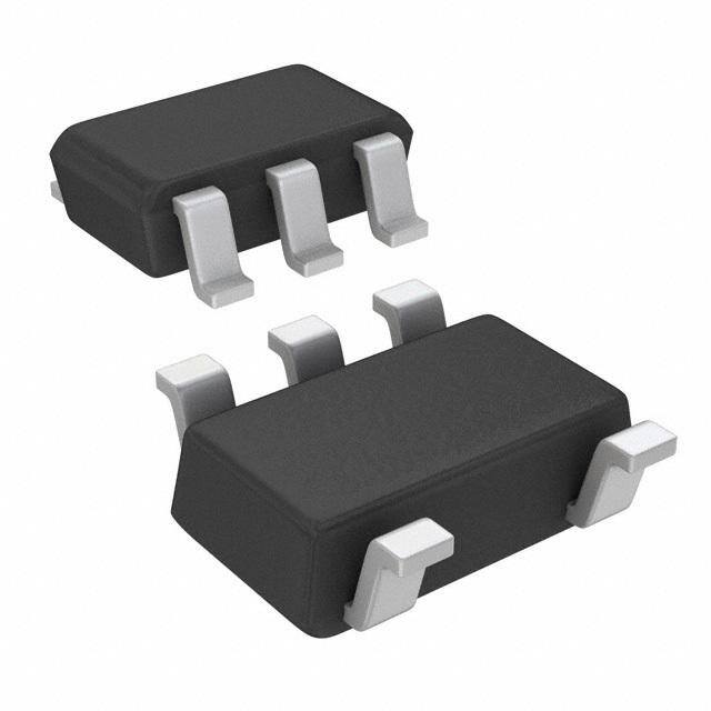
| 供应商器件封装 | SOT-23-5 |
| 其它名称 | 497-4666-1 |
| 其它有关文件 | http://www.st.com/web/catalog/sense_power/FM1946/SC792/PF91080?referrer=70071840 |
| 功率失效检测 | No |
| 包装 | 剪切带 (CT) |
| 受监控电压数 | 1 |
| 商标 | STMicroelectronics |
| 复位 | 低有效 |
| 复位超时 | 最小为 140 ms |
| 安装类型 | 表面贴装 |
| 安装风格 | SMD/SMT |
| 封装 | Reel |
| 封装/外壳 | SC-74A,SOT-753 |
| 封装/箱体 | SOT-23-5 |
| 工作温度 | -40°C ~ 85°C |
| 工作电源电流 | 12 uA |
| 工厂包装数量 | 3000 |
| 最大功率耗散 | 320 mW |
| 最大工作温度 | + 85 C |
| 最小工作温度 | - 40 C |
| 标准包装 | 1 |
| 欠电压阈值 | 3.04 V |
| 电压-阈值 | 3.08V |
| 电池备用开关 | No Backup |
| 电源电压-最大 | 7 V |
| 电源电压-最小 | 0.3 V |
| 监视器 | Watchdog |
| 类型 | 简单复位/加电复位 |
| 系列 | STM6822 |
| 芯片启用信号 | No Chip Enable |
| 被监测输入数 | 1 Input |
| 输出 | 开路漏极或开路集电极 |
| 输出类型 | Push-Pull |
| 过电压阈值 | 3.11 V |
| 重置延迟时间 | 280 ms |
| 阈值电压 | 2.5 V, 3 V, 3.3 V, 5 V |


- 商务部:美国ITC正式对集成电路等产品启动337调查
- 曝三星4nm工艺存在良率问题 高通将骁龙8 Gen1或转产台积电
- 太阳诱电将投资9.5亿元在常州建新厂生产MLCC 预计2023年完工
- 英特尔发布欧洲新工厂建设计划 深化IDM 2.0 战略
- 台积电先进制程称霸业界 有大客户加持明年业绩稳了
- 达到5530亿美元!SIA预计今年全球半导体销售额将创下新高
- 英特尔拟将自动驾驶子公司Mobileye上市 估值或超500亿美元
- 三星加码芯片和SET,合并消费电子和移动部门,撤换高东真等 CEO
- 三星电子宣布重大人事变动 还合并消费电子和移动部门
- 海关总署:前11个月进口集成电路产品价值2.52万亿元 增长14.8%


PDF Datasheet 数据手册内容提取
STM632x, STM682x 5-pin supervisor with watchdog timer and push-button reset Datasheet - production data Features • Precision V monitoring of 5, 3.3, 3, or 2.5 V CC power supplies • RST outputs (active low, push-pull or open drain) • RST outputs (active high, push-pull) • Reset pulse width of 1.4 ms, 200 ms and 240 ms (typ.) • Watchdog timeout period of 1.6 s (typ.) • Manual reset input (MR) • Low supply current - 3 µA (typ.) SOT23-5 (WY) • Guaranteed RST (RST) assertion down to V = 1.0 V CC • Operating temperature: –40 to +85 °C (industrial grade) • RoHS compliance Lead-free components are compliant with the RoHS directive Table 1. Device summary Reset output Watchdog Manual Part number input reset input Active low Active high Active low (push-pull) (push-pull) (open drain) STM6321 ✔ ✔ ✔ STM632x STM6322 ✔ ✔ ✔ STM6821 ✔ ✔ ✔ STM6822 ✔ ✔ ✔ STM682x STM6823 ✔ ✔ ✔ STM6824 ✔ ✔ ✔ STM6825 ✔ ✔ ✔ June 2016 DocID11110 Rev 13 1/31 This is information on a product in full production. www.st.com
Contents STM632x, STM682x Contents 1 Description . . . . . . . . . . . . . . . . . . . . . . . . . . . . . . . . . . . . . . . . . . . . . . . . . 5 1.1 Pin description . . . . . . . . . . . . . . . . . . . . . . . . . . . . . . . . . . . . . . . . . . . . . . 7 1.1.1 Active low, push-pull reset output (RST) - 6823/6824/6825 . . . . . . . . . . 7 1.1.2 Active low, open drain reset output (RST) - STM6321/6322/6822 . . . . . 7 1.1.3 Push-button reset input (MR) . . . . . . . . . . . . . . . . . . . . . . . . . . . . . . . . . . 7 1.1.4 Watchdog input (WDI) . . . . . . . . . . . . . . . . . . . . . . . . . . . . . . . . . . . . . . . 7 1.1.5 Active high reset output (RST) . . . . . . . . . . . . . . . . . . . . . . . . . . . . . . . . . 7 2 Operation . . . . . . . . . . . . . . . . . . . . . . . . . . . . . . . . . . . . . . . . . . . . . . . . . 10 2.1 Reset output . . . . . . . . . . . . . . . . . . . . . . . . . . . . . . . . . . . . . . . . . . . . . . . 10 2.2 Open drain RST output . . . . . . . . . . . . . . . . . . . . . . . . . . . . . . . . . . . . . . 10 2.3 Push-button reset input (STM6322/6821/6822/6823/6825) . . . . . . . . . . . .11 2.4 Watchdog input (STM6321/6821/6822/6823/6824) . . . . . . . . . . . . . . . . . .11 2.5 Applications information . . . . . . . . . . . . . . . . . . . . . . . . . . . . . . . . . . . . . . .11 2.5.1 Watchdog input current . . . . . . . . . . . . . . . . . . . . . . . . . . . . . . . . . . . . . 11 2.5.2 Ensuring a valid reset output down to V = 0 V . . . . . . . . . . . . . . . . . . 11 CC 2.6 Interfacing to microprocessors with bidirectional reset pins . . . . . . . . . . . 12 3 Typical operating characteristics . . . . . . . . . . . . . . . . . . . . . . . . . . . . . 13 4 Maximum ratings . . . . . . . . . . . . . . . . . . . . . . . . . . . . . . . . . . . . . . . . . . . 18 5 DC and AC parameters . . . . . . . . . . . . . . . . . . . . . . . . . . . . . . . . . . . . . . 19 6 Package information . . . . . . . . . . . . . . . . . . . . . . . . . . . . . . . . . . . . . . . . 24 6.1 SOT23-5 package information . . . . . . . . . . . . . . . . . . . . . . . . . . . . . . . . . 25 7 Part numbering . . . . . . . . . . . . . . . . . . . . . . . . . . . . . . . . . . . . . . . . . . . . 27 8 Revision history . . . . . . . . . . . . . . . . . . . . . . . . . . . . . . . . . . . . . . . . . . . 30 2/31 DocID11110 Rev 13
STM632x, STM682x List of tables List of tables Table 1. Device summary. . . . . . . . . . . . . . . . . . . . . . . . . . . . . . . . . . . . . . . . . . . . . . . . . . . . . . . . . . 1 Table 2. Signal names . . . . . . . . . . . . . . . . . . . . . . . . . . . . . . . . . . . . . . . . . . . . . . . . . . . . . . . . . . . . 5 Table 3. Pin function. . . . . . . . . . . . . . . . . . . . . . . . . . . . . . . . . . . . . . . . . . . . . . . . . . . . . . . . . . . . . . 7 Table 4. Absolute maximum ratings. . . . . . . . . . . . . . . . . . . . . . . . . . . . . . . . . . . . . . . . . . . . . . . . . 18 Table 5. Operating and AC measurement conditions. . . . . . . . . . . . . . . . . . . . . . . . . . . . . . . . . . . . 19 Table 6. DC and AC characteristics . . . . . . . . . . . . . . . . . . . . . . . . . . . . . . . . . . . . . . . . . . . . . . . . . 21 Table 7. SOT23-5 mechanical data . . . . . . . . . . . . . . . . . . . . . . . . . . . . . . . . . . . . . . . . . . . . . . . . . 25 Table 8. SOT23-5 carrier tape dimensions. . . . . . . . . . . . . . . . . . . . . . . . . . . . . . . . . . . . . . . . . . . . 26 Table 9. Ordering information scheme. . . . . . . . . . . . . . . . . . . . . . . . . . . . . . . . . . . . . . . . . . . . . . . 27 Table 10. Marking description. . . . . . . . . . . . . . . . . . . . . . . . . . . . . . . . . . . . . . . . . . . . . . . . . . . . . . . 28 Table 11. Document revision history . . . . . . . . . . . . . . . . . . . . . . . . . . . . . . . . . . . . . . . . . . . . . . . . . 30 DocID11110 Rev 13 3/31 3
List of figures STM632x, STM682x List of figures Figure 1. Logic diagram (STM6821/6822/6823) . . . . . . . . . . . . . . . . . . . . . . . . . . . . . . . . . . . . . . . . . 5 Figure 2. Logic diagram (STM6321/6322/6824/6825). . . . . . . . . . . . . . . . . . . . . . . . . . . . . . . . . . . . . 5 Figure 3. STM6822/6823 SOT23-5 connections. . . . . . . . . . . . . . . . . . . . . . . . . . . . . . . . . . . . . . . . . 6 Figure 4. STM6821 SOT23-5 connections . . . . . . . . . . . . . . . . . . . . . . . . . . . . . . . . . . . . . . . . . . . . . 6 Figure 5. STM6322/6825 SOT23-5 connections. . . . . . . . . . . . . . . . . . . . . . . . . . . . . . . . . . . . . . . . . 6 Figure 6. STM6321/6824 SOT23-5 connections. . . . . . . . . . . . . . . . . . . . . . . . . . . . . . . . . . . . . . . . . 6 Figure 7. Block diagram (STM6821/6822/6823) . . . . . . . . . . . . . . . . . . . . . . . . . . . . . . . . . . . . . . . . . 8 Figure 8. Block diagram (STM6321/6824). . . . . . . . . . . . . . . . . . . . . . . . . . . . . . . . . . . . . . . . . . . . . . 8 Figure 9. Block diagram (STM6322/6825). . . . . . . . . . . . . . . . . . . . . . . . . . . . . . . . . . . . . . . . . . . . . . 8 Figure 10. Hardware hookup. . . . . . . . . . . . . . . . . . . . . . . . . . . . . . . . . . . . . . . . . . . . . . . . . . . . . . . . . 9 Figure 11. STM6321/6322/6822 open drain RST output with multiple supplies . . . . . . . . . . . . . . . . . 10 Figure 12. Ensuring RST valid to V = 0, (active low push-pull outputs). . . . . . . . . . . . . . . . . . . . . . 12 CC Figure 13. Ensuring RST valid to V = 0, (active high, push-pull outputs) . . . . . . . . . . . . . . . . . . . . 12 CC Figure 14. Interfacing to microprocessors with bidirectional reset I/O. . . . . . . . . . . . . . . . . . . . . . . . . 12 Figure 15. V -to-reset output delay vs. temperature. . . . . . . . . . . . . . . . . . . . . . . . . . . . . . . . . . . . . 13 CC Figure 16. Supply current vs. temperature. . . . . . . . . . . . . . . . . . . . . . . . . . . . . . . . . . . . . . . . . . . . . . 13 Figure 17. MR-to-reset output delay vs. temperature . . . . . . . . . . . . . . . . . . . . . . . . . . . . . . . . . . . . . 14 Figure 18. Normalized power-up t vs. temperature . . . . . . . . . . . . . . . . . . . . . . . . . . . . . . . . . . . . . 14 rec Figure 19. Normalized reset threshold voltage vs. temperature . . . . . . . . . . . . . . . . . . . . . . . . . . . . . 15 Figure 20. Normalized power-up watchdog timeout period. . . . . . . . . . . . . . . . . . . . . . . . . . . . . . . . . 15 Figure 21. Voltage output low vs. I . . . . . . . . . . . . . . . . . . . . . . . . . . . . . . . . . . . . . . . . . . . . . . . . 16 SINK Figure 22. Voltage output high vs. I . . . . . . . . . . . . . . . . . . . . . . . . . . . . . . . . . . . . . . . . . . . . . 16 SOURCE Figure 23. Maximum transient duration vs. reset threshold overdrive. . . . . . . . . . . . . . . . . . . . . . . . . 17 Figure 24. AC testing input/output waveforms. . . . . . . . . . . . . . . . . . . . . . . . . . . . . . . . . . . . . . . . . . . 19 Figure 25. MR timing waveform. . . . . . . . . . . . . . . . . . . . . . . . . . . . . . . . . . . . . . . . . . . . . . . . . . . . . . 19 Figure 26. Watchdog timing. . . . . . . . . . . . . . . . . . . . . . . . . . . . . . . . . . . . . . . . . . . . . . . . . . . . . . . . . 20 Figure 27. SOT23-5 package outline. . . . . . . . . . . . . . . . . . . . . . . . . . . . . . . . . . . . . . . . . . . . . . . . . . 25 Figure 28. SOT23-5 carrier tape . . . . . . . . . . . . . . . . . . . . . . . . . . . . . . . . . . . . . . . . . . . . . . . . . . . . . 26 4/31 DocID11110 Rev 13
STM632x, STM682x Description 1 Description The STM6xxx supervisors are self-contained devices which provide microprocessor supervisory functions. A precision voltage reference and comparator monitors the V input CC for an out-of-tolerance condition. When an invalid V condition occurs, the reset output CC (RST) is forced low (or high in the case of RST). These devices also offer a watchdog timer (except for STM6322/6825) and/or a push-button (MR) reset input. These devices are available in a standard 5-pin SOT23 package. Figure 1. Logic diagram (STM6821/6822/6823) VCC WDI STM6XXX RST (RST)(1) MR VSS AI09128 1. For STM6821 only. Figure 2. Logic diagram (STM6321/6322/6824/6825) VCC RST (WDI)(1) MR STM6XXX RST VSS AI09129 1. For STM6321/6824. Table 2. Signal names Name Function MR Push-button reset input WDI Watchdog input RST Active low reset output RST Active high reset output V Supply voltage CC V Ground SS DocID11110 Rev 13 5/31 30
Description STM632x, STM682x Figure 3. STM6822/6823 SOT23-5 connections SOT23-5 RST(1) 1 5 VCC VSS 2 MR 3 4 WDI AI09130a 1. Open drain for STM6822. Figure 4. STM6821 SOT23-5 connections SOT23-5 RST(1) 1 5 VCC VSS 2 MR 3 4 WDI AI12285 1. Push-pull only. Figure 5. STM6322/6825 SOT23-5 connections SOT23-5 RST(1) 1 5 VCC VSS 2 RST(2) 3 4 MR AI09131a 1. Open drain for STM6322. 2. Push-pull only. Figure 6. STM6321/6824 SOT23-5 connections SOT23-5 RST(1) 1 5 VCC VSS 2 RST(2) 3 4 WDI AI12286 1. Open drain for STM6321. 2. Push-pull only. 6/31 DocID11110 Rev 13
STM632x, STM682x Description 1.1 Pin description 1.1.1 Active low, push-pull reset output (RST) - 6823/6824/6825 Pulses low when triggered, and stays low whenever V is below the reset threshold or CC when MR is a logic low. It remains low for t after either V rises above the reset rec CC threshold, the watchdog triggers a reset, or MR goes from low to high. 1.1.2 Active low, open drain reset output (RST) - STM6321/6322/6822 Pulses low when triggered, and stays low whenever V is below the reset threshold or CC when MR is a logic low. It remains low for t after either V rises above the reset rec CC threshold, the watchdog triggers a reset, or MR goes from low to high. Connect a pull-up resistor to supply voltage. 1.1.3 Push-button reset input (MR) A logic low on MR asserts the reset output. Reset remains asserted as long as MR is low and for t after MR returns high. This active low input has an internal 52 kΩ pull-up. It can rec be driven from a TTL or CMOS logic line, or shorted to ground with a switch. Leave open if unused. 1.1.4 Watchdog input (WDI) If WDI remains high or low for at least 1.6 s, the internal watchdog timer expires and reset is asserted. The internal watchdog timer clears while reset is asserted or when WDI sees a rising or falling edge. The watchdog function CAN be disabled if WDI is left unconnected or is connected to a tristate buffer output. 1.1.5 Active high reset output (RST) Active high, push-pull reset output; inverse of RST. Table 3. Pin function Pin Name Function STM6822 STM6321 STM6322 STM6821 STM6823 STM6824 STM6825 1 — 1 1 RST Active low reset output 3 3 — 4 MR Push-button reset input 4 4 4 — WDI Watchdog Input — 1 3 3 RST Active high reset output 5 5 5 5 V Supply voltage CC 2 2 2 2 V Ground SS DocID11110 Rev 13 7/31 30
Description STM632x, STM682x Figure 7. Block diagram (STM6821/6822/6823) (cid:58)(cid:39)(cid:44) (cid:58)(cid:36)(cid:55)(cid:38)(cid:43)(cid:39)(cid:50)(cid:42) (cid:58)(cid:39)(cid:44) (cid:87)(cid:85)(cid:68)(cid:81)(cid:86)(cid:76)(cid:87)(cid:76)(cid:82)(cid:81)(cid:68)(cid:79) (cid:55)(cid:44)(cid:48)(cid:40)(cid:53) (cid:71)(cid:72)(cid:87)(cid:72)(cid:70)(cid:87)(cid:82)(cid:85) (cid:57)(cid:38)(cid:38) (cid:57)(cid:38)(cid:38) (cid:57)(cid:53)(cid:54)(cid:55) (cid:38)(cid:50)(cid:48)(cid:51)(cid:36)(cid:53)(cid:40) (cid:74)(cid:72)(cid:81)(cid:87)(cid:85)(cid:72)(cid:72)(cid:85)(cid:70)(cid:68)(cid:87)(cid:82)(cid:85) (cid:53)(cid:54)(cid:55)(cid:3)(cid:11)(cid:53)(cid:54)(cid:55)(cid:12)(cid:11)(cid:20)(cid:15)(cid:21)(cid:12) (cid:48)(cid:53) (cid:36)(cid:44)(cid:19)(cid:28)(cid:20)(cid:22)(cid:21)(cid:57)(cid:21) 1. Push-pull for STM6823, open drain for STM6822. 2. Active high (push-pull) for STM6821. Figure 8. Block diagram (STM6321/6824) (cid:58)(cid:39)(cid:44) (cid:58)(cid:36)(cid:55)(cid:38)(cid:43)(cid:39)(cid:50)(cid:42) (cid:58)(cid:39)(cid:44) (cid:87)(cid:85)(cid:68)(cid:81)(cid:86)(cid:76)(cid:87)(cid:76)(cid:82)(cid:81)(cid:68)(cid:79) (cid:55)(cid:44)(cid:48)(cid:40)(cid:53) (cid:71)(cid:72)(cid:87)(cid:72)(cid:70)(cid:87)(cid:82)(cid:85) (cid:11)(cid:20)(cid:12) (cid:57)(cid:38)(cid:38) (cid:57)(cid:53)(cid:54)(cid:55) (cid:38)(cid:50)(cid:48)(cid:51)(cid:36)(cid:53)(cid:40) (cid:74)(cid:72)(cid:81)(cid:87)(cid:85)(cid:72)(cid:72)(cid:85)(cid:70)(cid:68)(cid:87)(cid:82)(cid:85) (cid:53)(cid:54)(cid:55)(cid:11)(cid:21)(cid:12) (cid:53)(cid:54)(cid:55) (cid:36)(cid:20)(cid:21)(cid:21)(cid:27)(cid:26)(cid:57)(cid:21) 1. Active low (open drain) for STM6321, active low (push-pull) for STM6824. 2. Push-pull only. Figure 9. Block diagram (STM6322/6825) (cid:57)(cid:38)(cid:38) (cid:87)(cid:85)(cid:72)(cid:70) (cid:53)(cid:54)(cid:55)(cid:11)(cid:20)(cid:12) (cid:57)(cid:38)(cid:38) (cid:57)(cid:53)(cid:54)(cid:55) (cid:38)(cid:50)(cid:48)(cid:51)(cid:36)(cid:53)(cid:40) (cid:74)(cid:72)(cid:81)(cid:72)(cid:85)(cid:68)(cid:87)(cid:82)(cid:85) (cid:53)(cid:54)(cid:55)(cid:11)(cid:21)(cid:12) (cid:48)(cid:53) (cid:36)(cid:44)(cid:20)(cid:21)(cid:21)(cid:27)(cid:27)(cid:57)(cid:21) 1. Active low (open drain) for STM6322, active low (push-pull) for STM6825. 2. Push-pull only. 8/31 DocID11110 Rev 13
STM632x, STM682x Description Figure 10. Hardware hookup (cid:57)(cid:38)(cid:38) (cid:57)(cid:38)(cid:38) (cid:54)(cid:55)(cid:48)(cid:25)(cid:59)(cid:59)(cid:59) (cid:41)(cid:85)(cid:82)(cid:80)(cid:3)(cid:80)(cid:76)(cid:70)(cid:85)(cid:82)(cid:83)(cid:85)(cid:82)(cid:70)(cid:72)(cid:86)(cid:86)(cid:82)(cid:85) (cid:58)(cid:39)(cid:44)(cid:11)(cid:20)(cid:12) (cid:11)(cid:21)(cid:12) (cid:48)(cid:53) (cid:51)(cid:88)(cid:86)(cid:75)(cid:16)(cid:69)(cid:88)(cid:87)(cid:87)(cid:82)(cid:81) (cid:11)(cid:22)(cid:12) (cid:53)(cid:54)(cid:55)(cid:3)(cid:11)(cid:53)(cid:54)(cid:55)(cid:12) (cid:55)(cid:82)(cid:3)(cid:80)(cid:76)(cid:70)(cid:85)(cid:82)(cid:83)(cid:85)(cid:82)(cid:70)(cid:72)(cid:86)(cid:86)(cid:82)(cid:85)(cid:3)(cid:85)(cid:72)(cid:86)(cid:72)(cid:87) (cid:11)(cid:23)(cid:12) (cid:53)(cid:54)(cid:55) (cid:55)(cid:82)(cid:3)(cid:80)(cid:76)(cid:70)(cid:85)(cid:82)(cid:83)(cid:85)(cid:82)(cid:70)(cid:72)(cid:86)(cid:86)(cid:82)(cid:85)(cid:3)(cid:85)(cid:72)(cid:86)(cid:72)(cid:87) (cid:36)(cid:44)(cid:19)(cid:28)(cid:20)(cid:22)(cid:22)(cid:57)(cid:21) 1. For STM6321/6821/6822/6823/6824. 2. For STM6322/6821/6822/6823/6825. 3. For STM6821/ (RST output only). 4. For STM6321/6322/6824/6825 (both RST and RST outputs). DocID11110 Rev 13 9/31 30
Operation STM632x, STM682x 2 Operation 2.1 Reset output The STM6xxx supervisor asserts a reset signal to the MCU whenever V goes below the CC reset threshold (V ), a watchdog timeout occurs, or when the push-button reset input RST (MR) is taken low. Reset is guaranteed valid for V < V down to V =1 V for CC RST CC T = 0 to 85 °C. A During power-up, once V exceeds the reset threshold an internal timer keeps reset low CC for the reset timeout period, t . After this interval reset is de-asserted. rec Each time RST is asserted, it stays low for at least the reset timeout period (t ). Any time rec V goes below the reset threshold the internal timer clears. The reset timer starts when CC V returns above the reset threshold. CC 2.2 Open drain RST output The STM6321/6322/6822 have an active low, open drain reset output. This output structure will sink current when RST is asserted. Connect a pull-up resistor from RST to any supply voltage up to 6 V (see Figure 11). Select a resistor value large enough to register a logic low, and small enough to register a logic high while supplying all input current and leakage paths connected to the reset output line. A 10 kΩ pull-up resistor is sufficient in most applications. Figure 11. STM6321/6322/6822 open drain RST output with multiple supplies (cid:22)(cid:17)(cid:22)(cid:3)(cid:57) (cid:24)(cid:17)(cid:19)(cid:3)(cid:57) (cid:57)(cid:38)(cid:38) (cid:54)(cid:55)(cid:48)(cid:25)(cid:59)(cid:59)(cid:59) (cid:24)(cid:3)(cid:57)(cid:3)(cid:86)(cid:92)(cid:86)(cid:87)(cid:72)(cid:80) (cid:11)(cid:20)(cid:12) (cid:48)(cid:53) (cid:11)(cid:21)(cid:12) (cid:58)(cid:39)(cid:44) (cid:11)(cid:22)(cid:12) (cid:53)(cid:54)(cid:55) (cid:53)(cid:54)(cid:55) (cid:42)(cid:49)(cid:39) (cid:36)(cid:44)(cid:19)(cid:28)(cid:20)(cid:22)(cid:26)(cid:57)(cid:21) 1. STM6322/6822. 2. STM6321/6822. 3. STM6321/6322. 10/31 DocID11110 Rev 13
STM632x, STM682x Operation 2.3 Push-button reset input (STM6322/6821/6822/6823/6825) A logic low on MR asserts reset. Reset remains asserted while MR is low, and for t (see rec Figure 25 on page 19) after it returns high. The MR input has an internal 52 kΩ pull-up resistor, allowing it to be left open if not used. This input can be driven with TTL/CMOS-logic levels or with open drain/collector outputs. Connect a normally open momentary switch from MR to GND to create a manual reset function; external debounce circuitry is not required. If MR is driven from long cables or the device is used in a noisy environment, connect a 0.1 µF capacitor from MR to GND to provide additional noise immunity. MR may float, or be tied to V when not used. CC 2.4 Watchdog input (STM6321/6821/6822/6823/6824) The watchdog timer can be used to detect an out-of-control MCU. If the MCU does not toggle the Watchdog Input (WDI) within t (1.6 sec), the reset is asserted. The internal WD watchdog timer is cleared by either: 1. a reset pulse, or 2. by toggling WDI (high to low or low to high), which can detect pulses as short as 50 ns. The timer remains cleared and does not count for as long as reset is asserted. As soon as reset is released, the timer starts counting. Note: The watchdog function may be disabled by floating WDI or tristating the driver connected to WDI. When tristated or disconnected, the maximum allowable leakage current is 10 µA and the maximum allowable load capacitance is 200 pF. 2.5 Applications information 2.5.1 Watchdog input current The WDI input is internally driven through a buffer and series resistor from the watchdog counter. For minimum watchdog input current (minimum overall power consumption), leave WDI low for the majority of the watchdog timeout period. When high, WDI can draw as much as 160 µA. Pulsing WDI high at a low duty cycle will reduce the effect of the large input current. When WDI is left unconnected, the watchdog timer is serviced within the watchdog timeout period by a low-high-low pulse from the counter chain. 2.5.2 Ensuring a valid reset output down to V = 0 V CC The STM6xxx supervisors are guaranteed to operate properly down to V = 1 V. In CC applications that require valid reset levels down to V = 0, a pull-down resistor to active CC low outputs (push/pull only, see Figure 12 on page 12) and a pull-up resistor to active high outputs (push/pull only, see Figure 13 on page 12) will ensure that the reset line is valid while the reset output can no longer sink or source current. This scheme does not work with the open drain outputs of the STM6321/6322/6822. The resistor value used is not critical, but it must be large enough not to load the reset output when V is above the reset threshold. For most applications, 100 kΩ is adequate. CC DocID11110 Rev 13 11/31 30
Operation STM632x, STM682x Figure 12. Ensuring RST valid to V = 0, (active low push-pull outputs) CC STM6XXX V CC V CC GND RST R1 AI09138 Figure 13. Ensuring RST valid to V = 0, (active high, push-pull outputs) CC V STM6XXX CC R1 V CC GND RST AI09139 1. This configuration does not work on open drain outputs of the STM6321/6322/6822. 2.6 Interfacing to microprocessors with bidirectional reset pins Microprocessors with bidirectional reset pins can contend with the STM6321 / 6322 / 6821 / 6822 / 6823 / 6824 / 6825 reset output. For example, if the reset output is driven high and the microprocessor wants to pull it low, signal contention will result. To prevent this from occurring, connect a 4.7 kΩ resistor between the reset output and the microprocessor’s reset I/O as in Figure 14. Figure 14. Interfacing to microprocessors with bidirectional reset I/O (cid:37)(cid:88)(cid:73)(cid:73)(cid:72)(cid:85)(cid:72)(cid:71)(cid:3)(cid:85)(cid:72)(cid:86)(cid:72)(cid:87)(cid:3)(cid:87)(cid:82)(cid:3)(cid:82)(cid:87)(cid:75)(cid:72)(cid:85) (cid:86)(cid:92)(cid:86)(cid:87)(cid:72)(cid:80)(cid:3)(cid:70)(cid:82)(cid:80)(cid:83)(cid:82)(cid:81)(cid:72)(cid:81)(cid:87)(cid:86) (cid:57)(cid:38)(cid:38) (cid:57)(cid:38)(cid:38) (cid:54)(cid:55)(cid:48)(cid:25)(cid:59)(cid:59)(cid:59) (cid:48)(cid:76)(cid:70)(cid:85)(cid:82)(cid:83)(cid:85)(cid:82)(cid:70)(cid:72)(cid:86)(cid:86)(cid:82)(cid:85) (cid:53)(cid:54)(cid:55) (cid:53)(cid:54)(cid:55) (cid:42)(cid:49)(cid:39) (cid:42)(cid:49)(cid:39) (cid:36)(cid:44)(cid:19)(cid:28)(cid:20)(cid:22)(cid:24)(cid:57)(cid:21) 12/31 DocID11110 Rev 13
STM632x, STM682x Typical operating characteristics 3 Typical operating characteristics Figure 15. V -to-reset output delay vs. temperature CC (cid:22)(cid:24) (cid:22)(cid:19) (cid:21)(cid:24) (cid:21)(cid:19) (cid:20)(cid:24) (cid:20)(cid:19) (cid:24) (cid:19) (cid:177)(cid:23)(cid:19) (cid:177)(cid:21)(cid:19) (cid:19) (cid:21)(cid:19) (cid:23)(cid:19) (cid:25)(cid:19) (cid:27)(cid:19) (cid:36)(cid:44)(cid:19)(cid:28)(cid:25)(cid:21)(cid:26)(cid:57)(cid:21) Figure 16. Supply current vs. temperature (cid:26) (cid:25) (cid:24) (cid:23) (cid:57)(cid:38)(cid:38)(cid:3)(cid:32)(cid:3)(cid:22)(cid:3)(cid:57) (cid:22) (cid:57)(cid:38)(cid:38)(cid:3)(cid:32)(cid:3)(cid:24)(cid:3)(cid:57) (cid:21) (cid:20) (cid:19) (cid:177)(cid:23)(cid:19) (cid:177)(cid:21)(cid:19) (cid:19) (cid:21)(cid:19) (cid:23)(cid:19) (cid:25)(cid:19) (cid:27)(cid:19) (cid:36)(cid:44)(cid:19)(cid:28)(cid:25)(cid:21)(cid:27)(cid:57)(cid:21) DocID11110 Rev 13 13/31 30
Typical operating characteristics STM632x, STM682x Figure 17. MR-to-reset output delay vs. temperature (cid:25)(cid:19)(cid:19) (cid:24)(cid:19)(cid:19) (cid:23)(cid:19)(cid:19) (cid:22)(cid:19)(cid:19) (cid:21)(cid:19)(cid:19) (cid:20)(cid:19)(cid:19) (cid:19) (cid:177)(cid:23)(cid:19) (cid:177)(cid:21)(cid:19) (cid:19) (cid:21)(cid:19) (cid:23)(cid:19) (cid:25)(cid:19) (cid:27)(cid:19) (cid:36)(cid:44)(cid:19)(cid:28)(cid:25)(cid:25)(cid:28)(cid:57)(cid:21) Figure 18. Normalized power-up t vs. temperature rec (cid:20)(cid:17)(cid:19)(cid:24) (cid:20)(cid:17)(cid:19)(cid:23) (cid:20)(cid:17)(cid:19)(cid:22) (cid:20)(cid:17)(cid:19)(cid:21) (cid:20)(cid:17)(cid:19)(cid:20) (cid:20)(cid:17)(cid:19)(cid:19) (cid:19)(cid:17)(cid:28)(cid:28) (cid:177)(cid:23)(cid:19) (cid:177)(cid:21)(cid:19) (cid:19) (cid:21)(cid:19) (cid:23)(cid:19) (cid:25)(cid:19) (cid:27)(cid:19) (cid:36)(cid:44)(cid:19)(cid:28)(cid:25)(cid:26)(cid:19)(cid:57)(cid:21) 14/31 DocID11110 Rev 13
STM632x, STM682x Typical operating characteristics Figure 19. Normalized reset threshold voltage vs. temperature (cid:20)(cid:17)(cid:19)(cid:24) (cid:20)(cid:17)(cid:19)(cid:23) (cid:20)(cid:17)(cid:19)(cid:22) (cid:20)(cid:17)(cid:19)(cid:21) (cid:20)(cid:17)(cid:19)(cid:20) (cid:20)(cid:17)(cid:19)(cid:19) (cid:19)(cid:17)(cid:28)(cid:28) (cid:19)(cid:17)(cid:28)(cid:27) (cid:19)(cid:17)(cid:28)(cid:26) (cid:19)(cid:17)(cid:28)(cid:25) (cid:19)(cid:17)(cid:28)(cid:24) (cid:177)(cid:23)(cid:19) (cid:177)(cid:21)(cid:19) (cid:19) (cid:21)(cid:19) (cid:23)(cid:19) (cid:25)(cid:19) (cid:27)(cid:19) (cid:36)(cid:44)(cid:19)(cid:28)(cid:25)(cid:22)(cid:20)(cid:57)(cid:21) Figure 20. Normalized power-up watchdog timeout period (cid:20)(cid:17)(cid:19)(cid:24) (cid:20)(cid:17)(cid:19)(cid:23) (cid:20)(cid:17)(cid:19)(cid:22) (cid:20)(cid:17)(cid:19)(cid:21) (cid:20)(cid:17)(cid:19)(cid:20) (cid:20)(cid:17)(cid:19)(cid:19) (cid:19)(cid:17)(cid:28)(cid:28) (cid:177)(cid:23)(cid:19) (cid:177)(cid:21)(cid:19) (cid:19) (cid:21)(cid:19) (cid:23)(cid:19) (cid:25)(cid:19) (cid:27)(cid:19) (cid:36)(cid:44)(cid:19)(cid:28)(cid:25)(cid:26)(cid:20)(cid:57)(cid:21) DocID11110 Rev 13 15/31 30
Typical operating characteristics STM632x, STM682x Figure 21. Voltage output low vs. I SINK (cid:19)(cid:17)(cid:22)(cid:24) (cid:19)(cid:17)(cid:22)(cid:19) (cid:19)(cid:17)(cid:21)(cid:24) (cid:19)(cid:17)(cid:21)(cid:19) (cid:57)(cid:38)(cid:38)(cid:3)(cid:32)(cid:3)(cid:21)(cid:17)(cid:28)(cid:3)(cid:57) (cid:19)(cid:17)(cid:20)(cid:24) (cid:19)(cid:17)(cid:20)(cid:19) (cid:19)(cid:17)(cid:19)(cid:24) (cid:19)(cid:17)(cid:19)(cid:19) (cid:19) (cid:20) (cid:21) (cid:22) (cid:23) (cid:24) (cid:25) (cid:36)(cid:44)(cid:19)(cid:28)(cid:25)(cid:22)(cid:23)(cid:57)(cid:21) Figure 22. Voltage output high vs. I SOURCE (cid:21)(cid:17)(cid:28)(cid:21) (cid:21)(cid:17)(cid:28)(cid:19) (cid:21)(cid:17)(cid:27)(cid:27) (cid:21)(cid:17)(cid:27)(cid:25) (cid:21)(cid:17)(cid:27)(cid:23) (cid:57)(cid:38)(cid:38)(cid:3)(cid:32)(cid:3)(cid:21)(cid:17)(cid:28)(cid:3)(cid:57) (cid:21)(cid:17)(cid:27)(cid:21) (cid:21)(cid:17)(cid:27)(cid:19) (cid:21)(cid:17)(cid:26)(cid:27) (cid:21)(cid:17)(cid:26)(cid:25) (cid:21)(cid:17)(cid:26)(cid:23) (cid:19)(cid:17)(cid:19) (cid:19)(cid:17)(cid:20) (cid:19)(cid:17)(cid:21) (cid:19)(cid:17)(cid:22) (cid:19)(cid:17)(cid:23) (cid:19)(cid:17)(cid:24) (cid:19)(cid:17)(cid:25) (cid:19)(cid:17)(cid:26) (cid:19)(cid:17)(cid:27) (cid:19)(cid:17)(cid:28) (cid:20)(cid:17)(cid:19) (cid:36)(cid:44)(cid:19)(cid:28)(cid:25)(cid:22)(cid:24)(cid:57)(cid:21) 16/31 DocID11110 Rev 13
STM632x, STM682x Typical operating characteristics Figure 23. Maximum transient duration vs. reset threshold overdrive (cid:22)(cid:24) (cid:22)(cid:19) (cid:21)(cid:24) (cid:54) (cid:21)(cid:19) (cid:61) (cid:20)(cid:24) (cid:47) (cid:20)(cid:19) (cid:24) (cid:19) (cid:19) (cid:21)(cid:19) (cid:23)(cid:19) (cid:25)(cid:19) (cid:27)(cid:19) (cid:20)(cid:19)(cid:19) (cid:20)(cid:21)(cid:19) (cid:20)(cid:23)(cid:19) (cid:20)(cid:25)(cid:19) (cid:20)(cid:27)(cid:19) (cid:21)(cid:19)(cid:19) (cid:36)(cid:44)(cid:19)(cid:28)(cid:25)(cid:22)(cid:26)(cid:57)(cid:21) DocID11110 Rev 13 17/31 30
Maximum ratings STM632x, STM682x 4 Maximum ratings Stressing the device above the rating listed in Table 4: Absolute maximum ratings may cause permanent damage to the device. These are stress ratings only and operation of the device at these or any other conditions above those indicated in Table 5: Operating and AC measurement conditions of this specification is not implied. Exposure to absolute maximum rating conditions for extended periods may affect device reliability. Refer also to the STMicroelectronics™ SURE program and other relevant quality documents. Table 4. Absolute maximum ratings Symbol Parameter Value Unit T Storage temperature (V off) –55 to 150 °C STG CC T (1) Lead solder temperature for 10 seconds 260 °C SLD V Input or output voltage –0.3 to V + 0.3 V IO CC V Supply voltage –0.3 to 7.0 V CC I Output current 20 mA O P Power dissipation 320 mW D 1. Reflow at peak temperature of 260 °C (total thermal budget not to exceed 245 °C for greater than 30 seconds). 18/31 DocID11110 Rev 13
STM632x, STM682x DC and AC parameters 5 DC and AC parameters This section summarizes the operating measurement conditions, and the DC and AC characteristics of the device. The parameters in Table 6: DC and AC characteristics, are derived from tests performed under the measurement conditions summarized in Table 5: Operating and AC measurement conditions. Designers should check that the operating conditions in their circuit match the operating conditions when relying on the quoted parameters. Table 5. Operating and AC measurement conditions Parameter STM6xxx Unit V supply voltage 1.0 to 5.5 V CC Ambient operating temperature (T ) –40 to 85 °C A Input rise and fall times ≤ 5 ns Input pulse voltages 0.2 to 0.8 V V CC Input and output timing ref. voltages 0.3 to 0.7 V V CC Figure 24. AC testing input/output waveforms (cid:19)(cid:17)(cid:27)(cid:3)(cid:57)(cid:38)(cid:38) (cid:19)(cid:17)(cid:26)(cid:3)(cid:57)(cid:38)(cid:38) (cid:19)(cid:17)(cid:22)(cid:3)(cid:57)(cid:38)(cid:38) (cid:19)(cid:17)(cid:21)(cid:3)(cid:57)(cid:38)(cid:38) (cid:36)(cid:44)(cid:19)(cid:21)(cid:24)(cid:25)(cid:27)(cid:57)(cid:20) Figure 25. MR timing waveform (cid:48)(cid:53) (cid:87)(cid:48)(cid:47)(cid:53)(cid:47) (cid:11)(cid:20)(cid:12) (cid:53)(cid:54)(cid:55)(cid:3) (cid:87)(cid:48)(cid:47)(cid:48)(cid:43) (cid:87)(cid:85)(cid:72)(cid:70) (cid:36)(cid:44)(cid:19)(cid:26)(cid:27)(cid:22)(cid:26)(cid:57)(cid:21) 1. RST for STM6322/6821/6825. DocID11110 Rev 13 19/31 30
DC and AC parameters STM632x, STM682x Figure 26. Watchdog timing (cid:57)(cid:38)(cid:38) (cid:53)(cid:54)(cid:55) (cid:87)(cid:85)(cid:72)(cid:70) (cid:58)(cid:39)(cid:44) (cid:87)(cid:58)(cid:39) (cid:36)(cid:44)(cid:19)(cid:28)(cid:20)(cid:22)(cid:25)(cid:57)(cid:21) 20/31 DocID11110 Rev 13
STM632x, STM682x DC and AC parameters Table 6. DC and AC characteristics Sym- Alter- Description Test condition(1) Min. Typ. Max. Unit bol native V Operating voltage 1.2 (2) 5.5 V CC VCC supply current T/S/R/Z/Y (VCC < 3.6 V) 4 12 µA (MR and WDI unconnected) L/M (V < 5.5 V) 6 17 µA CC I CC V supply current T/S/R/Z/Y (V < 3.6 V) 3 8 µA CC CC (MR unconnected; L/M (V < 5.5 V) 3 12 µA STM6322/6825) CC Input leakage current 0 V = V = V –1 +1 µA IN CC ILI Input leakage current WDI = VCC, time average 120 160 µA (WDI)(3) WDI = GND, time average –20 –15 µA I Open drain reset output VCC > VRST, –1 +1 µA LO leakage current Reset not asserted V > 4.0 V 2.0 V RST V Input high voltage (MR) IH V < 4.0 V 0.7 V V RST CC V Input high voltage (WDI)(4) V (max.) < V < 5.5 V 0.7 V V IH RST CC CC V > 4.0 V 0.8 V RST V Input low voltage (MR) IL V < 4.0 V 0.3 V V RST CC V Input low voltage (WDI)(4) V (max.) < V < 5.5 V 0.3 V V IL RST CC CC V ≥ 1.0 V, I = 50 µA, CC SINK 0.3 V Reset asserted V ≥ 1.2 V, I = 100 µA, CC SINK 0.3 V Output low voltage (RST; Reset asserted push-pull or open drain) V ≥ 2.7 V, I = 1.2 mA, CC SINK 0.3 V Reset asserted V OL V ≥ 4.5 V, I = 3.2 mA, CC SINK 0.4 V Reset asserted V ≥ 2.7 V, I = 1.2 mA, CC SINK 0.3 V Output low voltage (RST; Reset not asserted push-pull only) V ≥ 4.5 V, I = 3.2 mA, CC SINK 0.4 V Reset not asserted DocID11110 Rev 13 21/31 30
DC and AC parameters STM632x, STM682x Table 6. DC and AC characteristics (continued) Sym- Alter- Description Test condition(1) Min. Typ. Max. Unit bol native V ≥ 2.7 V, I = 500 µA, CC SOURCE 0.8 V V Reset not asserted CC Output high voltage (RST) V ≥ 4.5 V, I = 800 µA CC SOURCE 0.8 V V , Reset not asserted CC V ≥ 1.0 V, I = 1 µA, CC SOURCE 0.8 V V Reset asserted (0 °C to 85 °C) CC V OH V ≥ 1.5 V, I = 100 µA, CC SOURCE 0.8 V V Reset asserted CC Output high voltage (RST) V ≥ 2.55 V, I = 500 µA, CC SOURCE 0.8 V V Reset asserted CC V ≥ 4.25 V, I = 800 µA, CC SOURCE 0.8 V V Reset asserted CC Reset thresholds 25 °C 4.561 4.630 4.699 V STM6xxxL –40 to 85 °C 4.514 4.746 V 25 °C 4.314 4.390 4.446 V STM6xxxM –40 to 85 °C 4.270 4.490 V 25 °C 3.040 3.080 3.110 V STM6xxxT –40 to 85 °C 3.000 3.150 V 25 °C 2.890 2.930 2.960 V V (5) Reset threshold STM6xxxS RST –40 to 85 °C 2.857 3.000 V 25 °C 2.590 2.630 2.660 V STM6xxxR –40 to 85 °C 2.564 2.696 V 25 °C 2.266 2.300 2.335 V STM6xxxZ –40 to 85 °C 2.243 2.358 V 25 °C 1.970 2.000 2.030 V STM6xxxY –40 to 85 °C 1.950 2.050 V L/M versions 10 mV Reset threshold hysteresis T/S/R/Z/Y versions 5 mV V to RST delay CC (V – V = 100 mV, V 20 µs RST CC CC falling at 1 mV/µs) A 1 1.4 2 ms t (6) Reset pulse width Blank 140 200 280 ms rec J 240 360 480 ms 22/31 DocID11110 Rev 13
STM632x, STM682x DC and AC parameters Table 6. DC and AC characteristics (continued) Sym- Alter- Description Test condition(1) Min. Typ. Max. Unit bol native Reset threshold ppm/ 40 temperature coefficient C Push-button reset input t t MR pulse width 1 µs MLMH MR t t MR to RST output delay 500 ns MLRL MRD MR glitch immunity 100 ns MR pull-up resistor 35 52 75 kΩ Watchdog timer t (6) Watchdog timeout period 1.12 1.60 2.24 s WD WDI pulse width(7) V ≥ 3.0 V 50 ns CC 1. Valid for ambient operating temperature: T = –40 to 85 °C; V = 4.5 to 5.5 V for “L/M” versions; V = 2.7 to 3.6 V for A CC CC “T/S/R” versions; and V = 1.2 to 2.75 V for “Z/Y” version (except where noted). CC 2. V (min.) = 1.0 V for T = 0 to +85 °C. CC A 3. WDI input is designed to be driven by a three-state output device. To float WDI, the “high-impedance mode” of the output device must have a maximum leakage current of 10 µA and a maximum output capacitance of 200 pF. The output device must also be able to source and sink at least 200 µA when active. 4. WDI is internally serviced within the watchdog period if WDI is left unconnected. 5. The leakage current measured on the RST pin is tested with the reset asserted (output high impedance). 6. Other t offered for t (102 ms, 6.3 ms, and 25.6 s options). Minimum order quantities may apply. Contact local sales rec WD office for availability. 7. For V < 3.0 V, t (min.) = 100 ns. CC WD DocID11110 Rev 13 23/31 30
Package information STM632x, STM682x 6 Package information In order to meet environmental requirements, ST offers these devices in different grades of ECOPACK® packages, depending on their level of environmental compliance. ECOPACK specifications, grade definitions and product status are available at: www.st.com. ECOPACK is an ST trademark. 24/31 DocID11110 Rev 13
STM632x, STM682x Package information 6.1 SOT23-5 package information Figure 27. SOT23-5 package outline (cid:40) (cid:36)(cid:20) (cid:72) (cid:39) (cid:39)(cid:20) (cid:37) (cid:36)(cid:21) (cid:38) (cid:46) (cid:36) (cid:38)(cid:51) (cid:47) (cid:41) (cid:54)(cid:50)(cid:55)(cid:21)(cid:22)(cid:16)(cid:24) 1. Drawing is not to scale. Table 7. SOT23-5 mechanical data Dimensions Symbol mm inches Typ. Min. Max. Typ. Min. Max. A 1.20 0.90 1.45 0.047 0.035 0.057 A1 0.15 0.006 A2 1.05 0.90 1.30 0.041 0.035 0.051 B 0.40 0.35 0.50 0.016 0.014 0.020 C 0.15 0.09 0.20 0.006 0.004 0.008 D 2.90 2.80 3.00 0.114 0.110 0.118 D1 1.90 0.075 E 2.80 2.60 3.00 0.110 0.102 0.118 e 0.95 0.037 F 1.60 1.50 1.75 0.063 0.059 0.069 K 0° 10° 0° 10° L 0.35 0.10 0.60 0.014 0.004 0.024 DocID11110 Rev 13 25/31 30
Package information STM632x, STM682x Figure 28. SOT23-5 carrier tape P 0 E D P2 T A 0 F TOP COVER TAPE W B 0 P CENTER LINES 1 OF CAVITY K 0 USER DIRECTION OF FEED AM03073v1 Table 8. SOT23-5 carrier tape dimensions Bulk Package W D E P P F A B K P T Unit 0 2 0 0 0 1 qty. 8.00 1.50 1.75 4.00 2.00 3.50 3.23 3.17 1.37 4.00 0.254 SOT23-5 +0.30 +0.10/ mm 3000 ±0.10 ±0.10 ±0.10 ±0.05 ±0.10 ±0.10 ±0.10 ±0.10 ±0.013 –0.10 –0.00 26/31 DocID11110 Rev 13
STM632x, STM682x Part numbering 7 Part numbering Table 9. Ordering information scheme Example: STM6xxx L WY 6 E Device type STM6xxx Reset threshold voltage L: V = 4.514 to 4.746 V RST M: V = 4.270 to 4.490 V RST T: V = 3.000 to 3.150 V RST S: V = 2.850 to 3.000 V RST R: V = 2.564 to 2.696 V RST Z: V = 2.243 to 2.358 V RST Y: V = 1.950 to 2.050 V RST Reset pulse width(1) A: t = 1 to 2 ms rec Blank: t = 140 to 280 ms rec J: t = 240 to 480 ms rec Package WY = SOT23-5 Temperature range 6 = –40 to 85 °C Shipping method E = ECOPACK® package, tubes F = ECOPACK® package, tape and reel 1. Contact local sales office for availability. Other t offered for t (102 ms, 6.3 ms, and 25.6 s rec WD options). Minimum order quantities may apply. For other options, or for more information on any aspect of this device, please contact the ST sales office nearest you. DocID11110 Rev 13 27/31 30
Part numbering STM632x, STM682x Table 10. Marking description Part number Reset threshold (V) Reset pulse width (ms) Topside marking(1) STM6321LWY6F 4.630 200 5AU or 5AUx STM6321MAWY6F 4.390 1.4 5CR or 5CRx STM6321MWY6F 4.390 200 5AV or 5AVx STM6321TWY6F 3.080 200 5AW or 5AWx STM6321SWY6F 2.930 200 5AX or 5AXx STM6321RWY6F 2.630 200 5AY or 5AYx STM6322LWY6F 4.630 200 5BA or 5BAx STM6322MWY6F 4.390 200 5BB or 5BBx STM6322TWY6F 3.080 200 5BC or 5BCx STM6322SWY6F 2.930 200 5BD or 5BDx STM6322RWY6F 2.630 200 5BE or 5BEx STM6821LWY6F 4.630 200 5BG or 5BGx STM6821MWY6F 4.390 200 5BH or 5BHx STM6821TWY6F 3.080 200 5BJ or 5BJx STM6821SWY6F 2.930 200 5BK or 5BKx STM6821RWY6F 2.630 200 5BL or 5BLx STM6822LWY6F 4.630 200 5BN or 5BNx STM6822MWY6F 4.390 200 5BP or 5BPx STM6822TWY6F 3.080 200 5BQ or 5BQx STM6822SWY6F 2.930 200 5BR or 5BRx STM6822RWY6F 2.630 200 5BS or 5BSx STM6822ZWY6F 2.300 200 5BT or 5BTx STM6822YWY6F 2.000 200 5CT or 5CTx STM6823LWY6F 4.630 200 5BU or 5BUx STM6823MWY6F 4.390 200 5BV or 5BVx STM6823TJWY6F 3.080 280 5CM or 5CMx STM6823TWY6F 3.080 200 5BW or 5BWx STM6823SJWY6F 2.930 280 5CN or 5CNx STM6823SWY6F 2.930 200 5BX or 5BXx STM6823RJWY6F 2.630 280 5CP or 5CPx STM6823RWY6F 2.630 200 5BY or 5BYx STM6823ZWY6F 2.300 200 5BZ or 5BZx STM6824LWY6F 4.630 200 5CA or 5CAx STM6824MWY6F 4.390 200 5CB or 5CBx STM6824TWY6F 3.080 200 5CC or 5CCx 28/31 DocID11110 Rev 13
STM632x, STM682x Part numbering Table 10. Marking description (continued) Part number Reset threshold (V) Reset pulse width (ms) Topside marking(1) STM6824SWY6F 2.930 200 5CD or 5CDx STM6824RWY6F 2.630 200 5CE or 5CEx STM6825LWY6F 4.630 200 5CG or 5CGx STM6825MWY6F 4.390 200 5CH or 5CHx STM6825TWY6F 3.080 200 5CJ or 5CJx STM6825SWY6F 2.930 200 5CK or 5CKx STM6825RWY6F 2.630 200 5CL or 5CLx 1. Where “x” = assembly work week (A to Z), such that “A” = WW01-02, “B” = WW03-04, and so forth. DocID11110 Rev 13 29/31 30
Revision history STM632x, STM682x 8 Revision history Table 11. Document revision history Date Revision Changes 25-Aug-2004 1 First draft 15-Dec-2004 2 Update characteristics (Figure 15, 16, 17; Table 6, and 9) 10-Mar-2005 3 Document promoted to Datasheet status 17-Jun-2005 4 Package marking update (Table 10) Update characteristics, Lead-free text, availability (Figure 3, 4, 5, 6, 11-Apr-2006 5 7, 8, and 9; Table 1, 6, 9, and 10) 11-Aug-2006 6 Update Description, Table 9, and 10. 25-May-2007 7 Formatting changes, updated Table 10. Updated cover page; updated reset threshold values in Table 6, 9, 03-Jun-2008 8 and 10; addition of text to Section 6; updated Figure 27 and Table 6 and 7; minor text changes. Updated Section 1.1.1, Section 6; added tape and reel specifications 09-Apr-2009 9 Figure 28, Table 8. Document reformatted, Doc ID added, updated Table 10, corrected typo in Features, Section 1.1.4, Section 2.1, Section 2.3, Section 4, 06-Jan-2011 10 Table 4, Table 6, Table 9, Figure 7 to Figure 11, Figure 14 to Figure 26. Updated Table 10, corrected typo in Table 6, Table 7 and Table 8, 14-Jul-2011 11 reformatted Figure 27, updated Disclaimer. Removed note from Features, added cross-references to Section 4 27-Jun-2012 12 and Section 5, minor text corrections throughout document. Updated document layout 13-Jun-2016 13 Table 6: updated footnote 6 Table 9: updated footnote 1 30/31 DocID11110 Rev 13
STM632x, STM682x IMPORTANT NOTICE – PLEASE READ CAREFULLY STMicroelectronics NV and its subsidiaries (“ST”) reserve the right to make changes, corrections, enhancements, modifications, and improvements to ST products and/or to this document at any time without notice. Purchasers should obtain the latest relevant information on ST products before placing orders. ST products are sold pursuant to ST’s terms and conditions of sale in place at the time of order acknowledgement. Purchasers are solely responsible for the choice, selection, and use of ST products and ST assumes no liability for application assistance or the design of Purchasers’ products. No license, express or implied, to any intellectual property right is granted by ST herein. Resale of ST products with provisions different from the information set forth herein shall void any warranty granted by ST for such product. ST and the ST logo are trademarks of ST. All other product or service names are the property of their respective owners. Information in this document supersedes and replaces information previously supplied in any prior versions of this document. © 2016 STMicroelectronics – All rights reserved DocID11110 Rev 13 31/31 31
Mouser Electronics Authorized Distributor Click to View Pricing, Inventory, Delivery & Lifecycle Information: S TMicroelectronics: STM6824TWY6F STM6825MWY6F STM6823SWY6F STM6823MWY6F STM6322TWY6F STM6824LWY6F STM6321MAWY6F STM6822ZWY6F STM6821SWY6F STM6825TWY6F STM6824RWY6F STM6822SWY6F STM6321MWY6F STM6821MWY6F STM6823LWY6F STM6825LWY6F STM6321LWY6F STM6321RWY6F STM6321SWY6F STM6321TWY6F STM6322LWY6F STM6322MWY6F STM6322RWY6F STM6322SWY6F STM6821LWY6F STM6821RWY6F STM6821TWY6F STM6822LWY6F STM6822MWY6F STM6822RWY6F STM6822TWY6F STM6823RWY6F STM6823TWY6F STM6824MWY6F STM6824SWY6F STM6825RWY6F STM6825SWY6F STM6823TJWY6F STM6822YWY6F