ICGOO在线商城 > 集成电路(IC) > PMIC - 监控器 > STM6600CS25DM6F
 Datasheet下载
- 型号: STM6600CS25DM6F
- 制造商: STMicroelectronics
- 库位|库存: xxxx|xxxx
- 要求:
| 数量阶梯 | 香港交货 | 国内含税 |
| +xxxx | $xxxx | ¥xxxx |
查看当月历史价格
查看今年历史价格
STM6600CS25DM6F产品简介:
ICGOO电子元器件商城为您提供STM6600CS25DM6F由STMicroelectronics设计生产,在icgoo商城现货销售,并且可以通过原厂、代理商等渠道进行代购。 STM6600CS25DM6F价格参考。STMicroelectronicsSTM6600CS25DM6F封装/规格:PMIC - 监控器, 开路漏极或开路集电极 监控器 1 通道 12-TDFN(2x3)。您可以下载STM6600CS25DM6F参考资料、Datasheet数据手册功能说明书,资料中有STM6600CS25DM6F 详细功能的应用电路图电压和使用方法及教程。
STM6600CS25DM6F是由STMicroelectronics(意法半导体)制造的一款PMIC(电源管理集成电路)监控器,主要用于监控和保护便携式设备中的电池和电源系统。以下是其主要应用场景:

 1. 便携式电子设备
STM6600CS25DM6F广泛应用于便携式电子设备中,如智能手机、平板电脑、笔记本电脑、智能手表等。这些设备通常依赖于锂电池供电,而STM6600CS25DM6F可以实时监控电池电压、温度等参数,确保电池在安全范围内工作,防止过充、过放、过热等问题。

 2. 电池管理系统(BMS)
该芯片可以集成到电池管理系统中,用于监控电池的健康状态。它能够检测电池的电压、电流和温度,并通过内置的保护机制防止电池出现异常情况。例如,在电池电压过低时,它可以触发关机保护;在电池温度过高时,它可以限制充电或放电速率,延长电池寿命。

 3. 工业应用
在工业领域,STM6600CS25DM6F可用于监控各种电源系统的状态。例如,在自动化设备、机器人、医疗设备等场景中,电源的稳定性和安全性至关重要。STM6600CS25DM6F可以实时监控电源电压和电流,确保设备在正常的工作条件下运行,并在出现异常时及时发出警报或采取保护措施。

 4. 物联网(IoT)设备
随着物联网设备的普及,STM6600CS25DM6F也被广泛应用于各类低功耗、长时间运行的物联网设备中。它可以帮助这些设备优化电源管理,延长电池寿命,并确保设备在极端环境下也能正常工作。例如,在智能家居、环境监测、远程传感器等场景中,STM6600CS25DM6F可以有效监控电源状态,避免因电源问题导致设备故障。

 5. 可穿戴设备
在可穿戴设备中,如智能手环、健康监测设备等,STM6600CS25DM6F的应用也非常普遍。由于这些设备通常体积小巧且需要长时间续航,STM6600CS25DM6F可以在不影响设备性能的前提下,提供高效的电源管理和保护功能,确保用户在使用过程中不会遇到电池相关的问题。

总的来说,STM6600CS25DM6F凭借其高精度的监控能力和强大的保护功能,适用于多种需要高效电源管理和电池保护的场景,尤其是在便携式设备和物联网领域表现尤为突出。
| 参数 | 数值 |
| 产品目录 | 集成电路 (IC)半导体 |
| 描述 | IC SUPERVISOR 3.4V 12TDFN专业电源管理 Smart Push-button 3.40 V 200mV |
| 产品分类 | |
| 品牌 | STMicroelectronics |
| 产品手册 | |
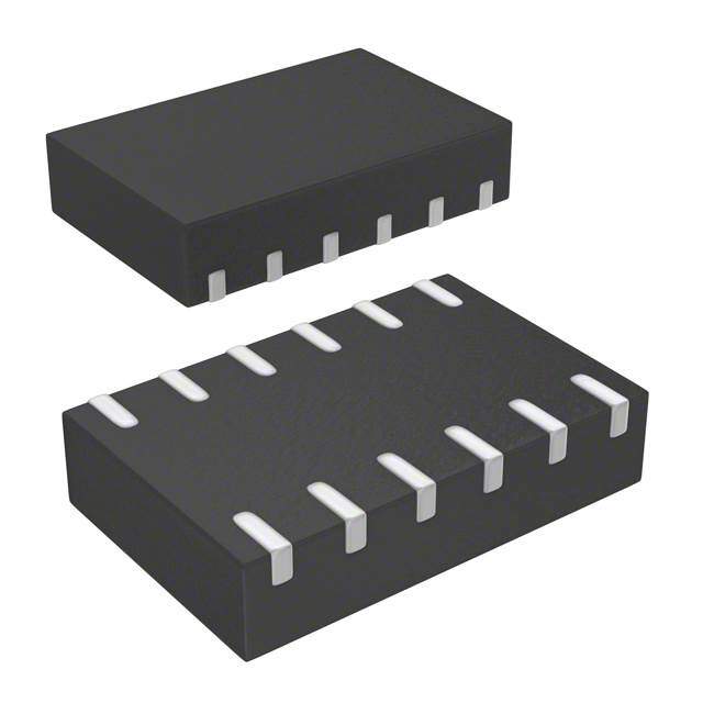
| 产品图片 |
|
| rohs | 符合RoHS无铅 / 符合限制有害物质指令(RoHS)规范要求 |
| 产品系列 | 电源管理 IC,专业电源管理,STMicroelectronics STM6600CS25DM6FSmart Reset™ |
| 数据手册 | |
| 产品型号 | STM6600CS25DM6F |
| 产品培训模块 | http://www.digikey.cn/PTM/IndividualPTM.page?site=cn&lang=zhs&ptm=25779 |
| 产品种类 | 专业电源管理 |
| 供应商器件封装 | 12-TDFN(2x3) |
| 其它名称 | 497-10550-1 |
| 其它有关文件 | http://www.st.com/web/catalog/sense_power/FM1946/SC1753/PF219701?referrer=70071840 |
| 包装 | 剪切带 (CT) |
| 受监控电压数 | 1 |
| 商标 | STMicroelectronics |
| 复位 | 低有效 |
| 复位超时 | - |
| 安装类型 | 表面贴装 |
| 安装风格 | SMD/SMT |
| 封装 | Reel |
| 封装/外壳 | 12-TDFN |
| 封装/箱体 | TDFN-12 |
| 工作温度 | -40°C ~ 85°C |
| 工作温度范围 | - 40 C to + 85 C |
| 工厂包装数量 | 3000 |
| 标准包装 | 1 |
| 电压-阈值 | 3.4V |
| 类型 | Smart On/Off |
| 系列 | STM6600 |
| 输出 | 开路漏极或开路集电极 |


- 商务部:美国ITC正式对集成电路等产品启动337调查
- 曝三星4nm工艺存在良率问题 高通将骁龙8 Gen1或转产台积电
- 太阳诱电将投资9.5亿元在常州建新厂生产MLCC 预计2023年完工
- 英特尔发布欧洲新工厂建设计划 深化IDM 2.0 战略
- 台积电先进制程称霸业界 有大客户加持明年业绩稳了
- 达到5530亿美元!SIA预计今年全球半导体销售额将创下新高
- 英特尔拟将自动驾驶子公司Mobileye上市 估值或超500亿美元
- 三星加码芯片和SET,合并消费电子和移动部门,撤换高东真等 CEO
- 三星电子宣布重大人事变动 还合并消费电子和移动部门
- 海关总署:前11个月进口集成电路产品价值2.52万亿元 增长14.8%


PDF Datasheet 数据手册内容提取
STM6600, STM6601 Smart push-button on/off controller with Smart Reset™ and power-on lockout Datasheet - production data • Debounced PB and SR inputs • PB and SR ESD inputs withstand voltage up to ±15 kV (air discharge) ±8 kV (contact discharge) • Active high or active low enable output option (EN or EN) provides control of MOSFET, DC-DC converter, regulator, etc. • Secure startup, interrupt, Smart Reset™ or power-down driven by push-button (cid:55)(cid:39)(cid:41)(cid:49)(cid:20)(cid:21) • Precise 1.5 V voltage reference with 1% accuracy • Industrial operating temperature –40 to +85 °C • Available in TDFN12 2 x 3 mm package Features Applications • Operating voltage 1.6 V to 5.5 V • Low standby current of 0.6 µA • Portable devices • Adjustable Smart Reset™ assertion delay time • Terminals driven by external CSRD • Audio and video players • Power-up duration determined primarily by • Cell phones and smart phones push-button press (STM6600) or by fixed time • PDAs, palmtops, organizers period, t (STM6601) ON_BLANK Table 1. Device summary Device RST C PB / SR EN or EN INT Startup process SRD PB must be held low until the STM6600 open drain(1) ✓ ✓ Push-pull Open drain(1) PS (2) confirmation HOLD PB can be released before the STM6601 open drain(1) ✓ ✓ Push-pull Open drain(1) PS (2) confirmation HOLD 1. External pull-up resistor needs to be connected to open drain outputs. 2. For a successful startup, the PS (power supply hold) needs to be pulled high within specific time, t . HOLD ON_BLANK October 2014 DocID15453 Rev 12 1/52 This is information on a product in full production. www.st.com
Contents STM6600, STM6601 Contents 1 Description . . . . . . . . . . . . . . . . . . . . . . . . . . . . . . . . . . . . . . . . . . . . . . . . . 5 2 Pin descriptions . . . . . . . . . . . . . . . . . . . . . . . . . . . . . . . . . . . . . . . . . . . . 9 3 Operation . . . . . . . . . . . . . . . . . . . . . . . . . . . . . . . . . . . . . . . . . . . . . . . . . 12 4 Waveforms . . . . . . . . . . . . . . . . . . . . . . . . . . . . . . . . . . . . . . . . . . . . . . . . 14 5 Typical operating characteristics . . . . . . . . . . . . . . . . . . . . . . . . . . . . . 28 6 Maximum ratings . . . . . . . . . . . . . . . . . . . . . . . . . . . . . . . . . . . . . . . . . . . 38 7 DC and AC characteristics . . . . . . . . . . . . . . . . . . . . . . . . . . . . . . . . . . . 39 8 Package mechanical data . . . . . . . . . . . . . . . . . . . . . . . . . . . . . . . . . . . . 42 9 Part numbering . . . . . . . . . . . . . . . . . . . . . . . . . . . . . . . . . . . . . . . . . . . . 46 10 Product selector . . . . . . . . . . . . . . . . . . . . . . . . . . . . . . . . . . . . . . . . . . . 49 11 Revision history . . . . . . . . . . . . . . . . . . . . . . . . . . . . . . . . . . . . . . . . . . . 51 2/52 DocID15453 Rev 12
STM6600, STM6601 List of tables List of tables Table 1. Device summary. . . . . . . . . . . . . . . . . . . . . . . . . . . . . . . . . . . . . . . . . . . . . . . . . . . . . . . . . . 1 Table 2. Pin descriptions . . . . . . . . . . . . . . . . . . . . . . . . . . . . . . . . . . . . . . . . . . . . . . . . . . . . . . . . . . 7 Table 3. Absolute maximum ratings. . . . . . . . . . . . . . . . . . . . . . . . . . . . . . . . . . . . . . . . . . . . . . . . . 38 Table 4. Operating and AC measurement conditions. . . . . . . . . . . . . . . . . . . . . . . . . . . . . . . . . . . . 39 Table 5. DC and AC characteristics . . . . . . . . . . . . . . . . . . . . . . . . . . . . . . . . . . . . . . . . . . . . . . . . . 39 Table 6. TDFN12 (2 x 3 mm) package mechanical data . . . . . . . . . . . . . . . . . . . . . . . . . . . . . . . . . 43 Table 7. Carrier tape dimensions for TDFN12 (2 x 3 mm) package. . . . . . . . . . . . . . . . . . . . . . . . . 45 Table 8. STM6600 ordering information scheme . . . . . . . . . . . . . . . . . . . . . . . . . . . . . . . . . . . . . . . 46 Table 9. STM6601 ordering information scheme . . . . . . . . . . . . . . . . . . . . . . . . . . . . . . . . . . . . . . . 48 Table 10. STM6600 product selector . . . . . . . . . . . . . . . . . . . . . . . . . . . . . . . . . . . . . . . . . . . . . . . . . 49 Table 11. STM6601 product selector . . . . . . . . . . . . . . . . . . . . . . . . . . . . . . . . . . . . . . . . . . . . . . . . . 50 Table 12. Document revision history . . . . . . . . . . . . . . . . . . . . . . . . . . . . . . . . . . . . . . . . . . . . . . . . . 51 DocID15453 Rev 12 3/52 3
List of figures STM6600, STM6601 List of figures Figure 1. Application hookup . . . . . . . . . . . . . . . . . . . . . . . . . . . . . . . . . . . . . . . . . . . . . . . . . . . . . . . 5 Figure 2. Basic functionality (option with enable deassertion after long push) . . . . . . . . . . . . . . . . . . 6 Figure 3. Basic functionality (option with RST assertion after long push) . . . . . . . . . . . . . . . . . . . . . . 6 Figure 4. Logic diagram. . . . . . . . . . . . . . . . . . . . . . . . . . . . . . . . . . . . . . . . . . . . . . . . . . . . . . . . . . . . 6 Figure 5. TDFN12 pin connections . . . . . . . . . . . . . . . . . . . . . . . . . . . . . . . . . . . . . . . . . . . . . . . . . . . 7 Figure 6. Block diagram. . . . . . . . . . . . . . . . . . . . . . . . . . . . . . . . . . . . . . . . . . . . . . . . . . . . . . . . . . . . 8 Figure 7. Successful power-up on STM6600 (PB released prior to t expiration) . . . . . . . . 14 ON_BLANK Figure 8. Successful power-up on STM6600 (t expires prior to PB release) . . . . . . . . . . . 15 ON_BLANK Figure 9. Unsuccessful power-up on STM6600 (PB released prior to t ) . . . . . . . . . . . . . . 16 ON_BLANK Figure 10. Unsuccessful power-up on STM6600 (t expires prior to PB release) . . . . . . . . . 17 ON_BLANK Figure 11. Successful power-up on STM6601. . . . . . . . . . . . . . . . . . . . . . . . . . . . . . . . . . . . . . . . . . . 18 Figure 12. Unsuccessful power-up on STM6601. . . . . . . . . . . . . . . . . . . . . . . . . . . . . . . . . . . . . . . . . . . . . . . . . . . .19 Figure 13. Power-up on STM660x with voltage dropout . . . . . . . . . . . . . . . . . . . . . . . . . . . . . . . . . . . 20 Figure 14. PB interrupt. . . . . . . . . . . . . . . . . . . . . . . . . . . . . . . . . . . . . . . . . . . . . . . . . . . . . . . . . . . . . 21 Figure 15. Long push, PB pressed first . . . . . . . . . . . . . . . . . . . . . . . . . . . . . . . . . . . . . . . . . . . . . . . . 22 Figure 16. Long push, SR pressed first. . . . . . . . . . . . . . . . . . . . . . . . . . . . . . . . . . . . . . . . . . . . . . . . 22 Figure 17. Invalid long push . . . . . . . . . . . . . . . . . . . . . . . . . . . . . . . . . . . . . . . . . . . . . . . . . . . . . . . . 23 Figure 18. Long push (option with RST assertion). . . . . . . . . . . . . . . . . . . . . . . . . . . . . . . . . . . . . . . . 24 Figure 19. Long push (option with enable deassertion) . . . . . . . . . . . . . . . . . . . . . . . . . . . . . . . . . . . 25 Figure 20. Undervoltage detected for <t . . . . . . . . . . . . . . . . . . . . . . . . . . . . . . . . . . . . . . . . . . . . 26 SRD Figure 21. Undervoltage detected for >t . . . . . . . . . . . . . . . . . . . . . . . . . . . . . . . . . . . . . . . . . . . . 26 SRD Figure 22. PB output waveform. . . . . . . . . . . . . . . . . . . . . . . . . . . . . . . . . . . . . . . . . . . . . . . . . . . 27 OUT Figure 23. Supply current vs. temperature, normal state. . . . . . . . . . . . . . . . . . . . . . . . . . . . . . . . . . . 28 Figure 24. Supply current vs. temperature, standby state. . . . . . . . . . . . . . . . . . . . . . . . . . . . . . . . . . 28 Figure 25. Supply current vs. supply voltage, normal state. . . . . . . . . . . . . . . . . . . . . . . . . . . . . . . . . 29 Figure 26. Supply current vs. supply voltage, standby state . . . . . . . . . . . . . . . . . . . . . . . . . . . . . . . . 29 Figure 27. Threshold vs. temperature, V = 3.4 V (typ.) . . . . . . . . . . . . . . . . . . . . . . . . . . . . . . . . . 30 TH+ Figure 28. Threshold hysteresis vs. temperature, V = 200 mV (typ.). . . . . . . . . . . . . . . . . . . . . . 30 HYST Figure 29. Debounce period vs. supply voltage. . . . . . . . . . . . . . . . . . . . . . . . . . . . . . . . . . . . . . . . . . 31 Figure 30. C charging current vs. temperature, V = 3.6 V. . . . . . . . . . . . . . . . . . . . . . . . . . . . . 31 SRD CC Figure 31. Output low voltage vs. output low current, T = 25 °C . . . . . . . . . . . . . . . . . . . . . . . . . . . . 32 A Figure 32. Output high voltage vs. output high current, T = 25 °C. . . . . . . . . . . . . . . . . . . . . . . . . . . 32 A Figure 33. Output voltage vs. supply voltage, I = 1 mA, T = 25 °C . . . . . . . . . . . . . . . . . . . . . . . 33 OUT A Figure 34. Input voltage vs. temperature. . . . . . . . . . . . . . . . . . . . . . . . . . . . . . . . . . . . . . . . . . . . . . . 33 Figure 35. Reference output voltage vs. temperature, V = 2.0 V. . . . . . . . . . . . . . . . . . . . . . . . . . . 34 CC Figure 36. Reference output voltage vs. load current, V = 2.0 V, T = 25 °C . . . . . . . . . . . . . . . . . 34 CC A Figure 37. Reference output voltage vs. supply voltage, T = 25 °C. . . . . . . . . . . . . . . . . . . . . . . . . . 35 A Figure 38. Reference startup, I = 15 µF, T = 25 °C . . . . . . . . . . . . . . . . . . . . . . . . . . . . . . . . . . . 35 REF A Figure 39. Reference response to steps on supply voltage, I = 15 µA, T = 25 °C. . . . . . . . . . . . 36 REF A Figure 40. Reference response to steps in load current, V = 3.6 V, T = 25 °C . . . . . . . . . . . . . . . 37 CC A Figure 41. TDFN12 (2 x 3 mm) package outline . . . . . . . . . . . . . . . . . . . . . . . . . . . . . . . . . . . . . . . . . 43 Figure 42. TDFN12 (2 x 3 mm) recommended footprint . . . . . . . . . . . . . . . . . . . . . . . . . . . . . . . . . . . 44 Figure 43. Carrier tape for TDFN12 (2 x 3 mm) package . . . . . . . . . . . . . . . . . . . . . . . . . . . . . . . . . . 45 4/52 DocID15453 Rev 12
STM6600, STM6601 Description 1 Description The STM6600-01 devices monitor the state of connected push-button(s) as well as sufficient supply voltage. An enable output controls power for the application through the MOSFET transistor, DC-DC converter, regulator, etc. If the supply voltage is above a precise voltage threshold, the enable output can be asserted by a simple press of the button. Factory-selectable supply voltage thresholds are determined by highly accurate and temperature-compensated references. An interrupt is asserted by pressing the push-button during normal operation and can be used to request a system power-down. The interrupt is also asserted if undervoltage is detected. By a long push of one button (PB) or two buttons (PB and SR) either a reset is asserted or power for the application is disabled depending on the option used. The device also offers additional features such as precise 1.5 V voltage reference with very tight accuracy of 1%, separate output indicating undervoltage detection and separate output for distinguishing between interrupt by push-button or undervoltage. The device consumes very low current of 6 µA during normal operation and only 0.6 µA current during standby. The STM6600-01 is available in the TDFN12 package and is offered in several options among features such as selectable threshold, hysteresis, timeouts, output types, etc. Figure 1. Application hookup (cid:39)(cid:39)(cid:38)(cid:38)(cid:16)(cid:16)(cid:39)(cid:39)(cid:38)(cid:38)(cid:3)(cid:3)(cid:70)(cid:70)(cid:82)(cid:82)(cid:81)(cid:81)(cid:89)(cid:89)(cid:72)(cid:72)(cid:85)(cid:85)(cid:87)(cid:87)(cid:72)(cid:72)(cid:85)(cid:85)(cid:15)(cid:15) (cid:83)(cid:83)(cid:82)(cid:82)(cid:90)(cid:90)(cid:72)(cid:72)(cid:85)(cid:85)(cid:3)(cid:3)(cid:48)(cid:48)(cid:50)(cid:50)(cid:54)(cid:54)(cid:41)(cid:41)(cid:40)(cid:40)(cid:55)(cid:55)(cid:15)(cid:15) (cid:85)(cid:85)(cid:72)(cid:72)(cid:74)(cid:74)(cid:88)(cid:88)(cid:79)(cid:79)(cid:68)(cid:68)(cid:87)(cid:87)(cid:82)(cid:82)(cid:85)(cid:85)(cid:15)(cid:15)(cid:3)(cid:3)(cid:72)(cid:72)(cid:87)(cid:87)(cid:70)(cid:70)(cid:17)(cid:17) (cid:53)(cid:53)(cid:20)(cid:20) (cid:47)(cid:47)(cid:40)(cid:40)(cid:39)(cid:39) (cid:57)(cid:57)(cid:38)(cid:38)(cid:38)(cid:38) (cid:40)(cid:40)(cid:49)(cid:49)(cid:3)(cid:3)(cid:11)(cid:11)(cid:40)(cid:40)(cid:49)(cid:49)(cid:12)(cid:12) (cid:53)(cid:53)(cid:22)(cid:22)(cid:11)(cid:11)(cid:20)(cid:20)(cid:12)(cid:12) (cid:53)(cid:53)(cid:23)(cid:23)(cid:11)(cid:11)(cid:20)(cid:20)(cid:12)(cid:12) (cid:53)(cid:53)(cid:24)(cid:24)(cid:11)(cid:11)(cid:20)(cid:20)(cid:12)(cid:12) (cid:57)(cid:57)(cid:39)(cid:39)(cid:39)(cid:39) (cid:53)(cid:53)(cid:54)(cid:54)(cid:55)(cid:55) (cid:53)(cid:53)(cid:54)(cid:54)(cid:55)(cid:55) (cid:57)(cid:57)(cid:38)(cid:38)(cid:38)(cid:38)(cid:47)(cid:47)(cid:50)(cid:50) (cid:51)(cid:51)(cid:37)(cid:37) (cid:51)(cid:51)(cid:54)(cid:54)(cid:43)(cid:43)(cid:50)(cid:50)(cid:47)(cid:47)(cid:39)(cid:39) (cid:44)(cid:44)(cid:18)(cid:18)(cid:50)(cid:50) (cid:54)(cid:54)(cid:55)(cid:55)(cid:48)(cid:48)(cid:25)(cid:25)(cid:25)(cid:25)(cid:19)(cid:19)(cid:19)(cid:19) (cid:44)(cid:44)(cid:49)(cid:49)(cid:55)(cid:55) (cid:49)(cid:49)(cid:48)(cid:48)(cid:44)(cid:44)(cid:3)(cid:3)(cid:82)(cid:82)(cid:85)(cid:85)(cid:3)(cid:3)(cid:44)(cid:44)(cid:49)(cid:49)(cid:55)(cid:55) (cid:11)(cid:11)(cid:22)(cid:22)(cid:12)(cid:12) (cid:54)(cid:54)(cid:55)(cid:55)(cid:48)(cid:48)(cid:25)(cid:25)(cid:25)(cid:25)(cid:19)(cid:19)(cid:20)(cid:20) (cid:51)(cid:51)(cid:37)(cid:37)(cid:50)(cid:50)(cid:56)(cid:56)(cid:55)(cid:55) (cid:44)(cid:44)(cid:18)(cid:18)(cid:50)(cid:50) (cid:54)(cid:54)(cid:53)(cid:53) (cid:57)(cid:57)(cid:53)(cid:53)(cid:40)(cid:40)(cid:41)(cid:41) (cid:48)(cid:48)(cid:38)(cid:38)(cid:56)(cid:56) (cid:38)(cid:38)(cid:51)(cid:51)(cid:56)(cid:56) (cid:42)(cid:42)(cid:49)(cid:49)(cid:39)(cid:39) (cid:38)(cid:38)(cid:54)(cid:54)(cid:53)(cid:53)(cid:39)(cid:39) (cid:38)(cid:38)(cid:53)(cid:53)(cid:40)(cid:40)(cid:41)(cid:41)(cid:11)(cid:11)(cid:21)(cid:21)(cid:12)(cid:12) (cid:37)(cid:37)(cid:36)(cid:36)(cid:54)(cid:54)(cid:40)(cid:40)(cid:37)(cid:37)(cid:36)(cid:36)(cid:49)(cid:49)(cid:39)(cid:39) (cid:38)(cid:38)(cid:54)(cid:54)(cid:53)(cid:53)(cid:39)(cid:39) (cid:36)(cid:36)(cid:48)(cid:48)(cid:19)(cid:19)(cid:19)(cid:19)(cid:21)(cid:21)(cid:23)(cid:23)(cid:25)(cid:25)(cid:89)(cid:89)(cid:23)(cid:23) 1. A resistor is required for open drain output type only. A 10 kΩ pull-up is sufficient in most applications. 2. Capacitor C is mandatory on V output (even if V is not used). Capacitor value of 1 µF is recommended. REF REF REF 3. For the STM6601 the processor has to confirm the proper power-on during the fixed time period, t . This failsafe ON_BLANK feature prevents the user from turning on the system when there is a faulty power switch or an unresponsive microprocessor. DocID15453 Rev 12 5/52 51
Description STM6600, STM6601 Figure 2. Basic functionality (option with enable deassertion after long push) POWER-UP(1) INTERRUPT POWER-DOWN (short push) (long push) PB SR EN INT interrupt interrupt AM00243v1 1. For power-up the battery voltage has to be above V threshold. TH+ Figure 3. Basic functionality (option with RST assertion after long push) POWER-UP(1) INTERRUPT POWER-DOWN (short push) (long push) PB SR RST INT interrupt interrupt AM00243bv1 1. For power-up the battery voltage has to be above V threshold. TH+ Figure 4. Logic diagram VCC EN (EN) PB RST SR INT STM6600 PS STM6601 PBOUT HOLD CSRD VCCLO VREF GND AM00236v1 6/52 DocID15453 Rev 12
STM6600, STM6601 Description Table 2. Pin descriptions Pin number Symbol Function 1 V Power supply input CC 2 SR Smart Reset™ button input 3 V Precise 1.5 V voltage reference REF 4 PS PS input HOLD HOLD 5 C Adjustable Smart Reset™ delay time input SRD 6 PB Push-button input 7 VCC Output for high threshold comparator output (V ) LO TH+ 8 PB Status of PB push-button input OUT 9 EN or EN Enable output 10 RST Reset output 11 INT Interrupt output 12 GND Ground Figure 5. TDFN12 pin connections VCC 1 12 GND SR 2 11 INT VREF 3 10 RST PS 4 9 EN (EN) HOLD C 5 8 PB SRD OUT PB 6 7 VCC LO AM00245v1 DocID15453 Rev 12 7/52 51
Description STM6600, STM6601 Figure 6. Block diagram VCCLO VCC EN (EN) + + tREC RST VCC VCC – – generator PS R (1) R (2) VTH+ VTH– HOLD PB SR Smart PB Glitch immunity logic R (3) PSHOLD Edge detectordebounce INT SR Glitch immunity Edge detectordebounce VREF GND SRD logic 1.5 V PBOUT CSRD AM00237v3 1. Internal pull-up resistor connected to PB input (see Table 5 for precise specifications). 2. Optional internal pull-up resistor connected to SR input (see Table 5 for precise specifications and Table 10 for detailed device options). 3. Internal pull-down resistor is connected to PS input only during startup (see Figure 7, 8, 9, 10, 11, 12, 13, and 18). HOLD 8/52 DocID15453 Rev 12
STM6600, STM6601 Pin descriptions 2 Pin descriptions V - power supply input CC V is monitored during startup and normal operation for sufficient voltage level. Decouple CC the V pin from ground by placing a 0.1 µF capacitor as close to the device as possible. CC SR - Smart Reset™ button input This input is equipped with voltage detector with a factory-trimmed threshold and has ±8 kV HBM ESD protection. Both PB and SR buttons have to be pressed and held for t period so the long push is SRD recognized and the reset is asserted (or the enable output is deasserted depending on the option) - see Figure 15, 16, and 17. Active low SR input is usually connected to GND through the momentary push-button (see Figure 1) and it has an optional 100 kΩ pull-up resistor. It is also possible to drive this input using an external device with either open drain (recommended) or push-pull output. Open drain output can be connected in parallel with push-button or other open drain outputs, which is not possible with push-pull output. SR input is monitored for falling edge after power-up and must not be grounded permanently. V - external precise 1.5 V voltage reference REF This 1.5 V voltage reference is specified with very tight accuracy of 1% (see Table 5). It has proper output voltage as soon as the reset output is deasserted (i.e. after t expires) and REC it is disabled when the device enters standby mode. A mandatory capacitor needs to be connected to V output (even if V is not used). Capacitor value of 1 µF is REF REF recommended. PS input HOLD This input is equipped with a voltage detector with a factory-trimmed threshold. It is used to confirm correct power-up of the device (if EN or EN is not asserted) or to initiate a shutdown (if EN or EN is asserted). Forcing PS high during power-up confirms the proper start of the application and keeps HOLD enable output asserted. Because most processors have outputs in high-Z state before initialization, an internal pull-down resistor is connected to PS input during startup (see HOLD Figure 7, 8, 9, 10, 11, 12, 13, and 18). Forcing the PS signal low during normal operation deasserts the enable output (see HOLD Figure 14). Input voltage on this pin is compared to an accurate voltage reference. C - Smart Reset™ delay time input SRD A capacitor to ground determines the additional time (t ) that PB with SR must be SRD pressed and held before a long push is recognized. The connected C capacitor is SRD charged with I current. Additional Smart Reset™ delay time t ends when voltage on SRD SRD the C capacitor reaches the V voltage threshold. It is recommended to use a low SRD SRD ESR capacitor (e.g. ceramic). If the capacitor is not used, leave the C pin open. If no SRD capacitor is connected, there is no t and a long push is recognized right after t SRD INT_Min expires (see Figure 18 and 19). DocID15453 Rev 12 9/52 51
Pin descriptions STM6600, STM6601 PB - power ON switch This input is equipped with a voltage detector with a factory-trimmed threshold and has ± 8 kV HBM ESD protection. When the PB button is pressed and held, the battery voltage is detected and EN (or EN) is asserted if the battery voltage is above the threshold V during the whole t TH+ DEBOUNCE period (see Figure 13). A short push of the push-button during normal operation can initiate an interrupt through debounced INT output (see Figure 14) and a long push of PB and SR simultaneously can either assert reset output RST (see Figure 18) or deassert the EN or EN output (see Figure 19) based on the option used. Note: A switch to GND must be connected to this input (e.g. mechanical push-button, open drain output of external circuitry, etc.), see Figure 1. This ensures a proper startup signal on PB (i.e. a transition from full V below specified V ). PB input has an internal 100 kΩ pull-up CC IL resistor connected. VCC - high threshold detection output LO During power-up, VCC is low when V supply voltage is below the V threshold. After LO CC TH+ successful power-up (i.e. during normal operation) VCC is low anytime undervoltage is LO detected (see Figure 13). Output type is active low and open drain by default. Open drain output type requires a pull- up resistor. A 10 kΩ is sufficient in most applications. VCC is floating when STM660x is in standby mode. LO PB - PB input state OUT If the push-button PB is pressed, the pin stays low during the t time period. DEBOUNCE If PB is asserted for the entire t period, PB will then stay low for at least DEBOUNCE OUT t . If PB is asserted after t expires, PB will return high as soon as PB is INT_Min INT_Min OUT deasserted (see Figure 22). PB ignores PB assertion during an undervoltage condition. OUT At startup on the STM6601 PB will respond only to the first PB assertion and any other OUT assertion will be ignored until t expires. This output is active low and open drain by ON_BLANK default. Open drain output type requires a pull-up resistor. A 10 kΩ is sufficient in most applications. 10/52 DocID15453 Rev 12
STM6600, STM6601 Pin descriptions EN or EN - enable output This output is intended to enable system power (see Figure 1). EN is asserted high after a valid turn-on event has been detected and confirmed (i.e. push-button has been pressed and held for t or more and V > V voltage level has been detected - see DEBOUNCE CC TH+ Figure 13). EN is released low if any of the conditions below occur: a) the push-button is released before PS is driven high (valid for STM6600, see HOLD Figure 9) or t expires before PS is driven high during startup (valid ON_BLANK HOLD for both STM6600 and STM6601, see Figure 10 and 12). b) PS is driven low during normal operation (see Figure 14). HOLD c) an undervoltage condition is detected for more than t + t + t SRD INT_Min DEBOUNCE (see Figure 21). d) a long push of the buttons is detected (only for the device with option “EN deasserted by long push” - see Figure 19) or PS is not driven high during HOLD t after a long push of the buttons (only for the device with option “RST ON_BLANK asserted by long push” - see Figure 18). Described logic levels are inverted in case of EN output. Output type is push-pull by default. RST - reset output This output pulls low for t : REC a) during startup. PB has been pressed (falling edge on the PB detected) and held for at least t and V > V (see Figure 7, 8, 9, 10, 11, 12 and 13 for DEBOUNCE CC TH+ more details). b) after long push detection (valid only for the device with option “RST asserted by long push”). PB has been pressed (falling edge on the PB detected) and held for more than t + t (additional Smart Reset™ delay time can be adjusted DEBOUNCE SRD by the external capacitor C ) - see Figure 18. SRD Output type is active low and open drain by default. Open drain output type requires a pull- up resistor. A 10 kΩ is sufficient in most applications. INT - interrupt output While the system is under normal operation (PS is driven high, power for application is HOLD asserted), the INT is driven low if: a) V falls below V threshold (i.e. undervoltage is detected - see Figure 20 and CC TH- 21). b) the falling edge on the PB is detected and the push-button is held for t DEBOUNCE or more. INT is driven low after t and stays low as long as PB is held. DEBOUNCE The INT signal is held high during power-up. The state of the PB output can be used to determine if the interrupt was caused by OUT either the assertion of the PB input, or was due to the detection of an undervoltage condition on V . CC INT output is asserted low for at least t . INT_Min Output type is active low and open drain by default. Open drain output type requires a pull- up resistor. A 10 kΩ is sufficient in most applications. GND - ground DocID15453 Rev 12 11/52 51
Operation STM6600, STM6601 3 Operation ™ The STM6600-STM6601 simplified smart push-button on/off controller with Smart Reset and power-on lockout enables and disables power for the application depending on push- button states, signals from the processor, and battery voltage. Power-on Because most of the processors have outputs in high-Z state before initialization, an internal pull-down resistor is connected to PS input during startup (see Figure 7, 8, 9, 10, 11, HOLD 12, 13, and 18). To power up the device the push-button PB has to be pressed for at least t and DEBOUNCE V has to be above V for the whole t period. If the battery voltage drops CC TH+ DEBOUNCE below V during the t , the counter is reset and starts to count again when V > TH+ DEBOUNCE CC V (see Figure 13). After t the enable signal is asserted (EN goes high, EN TH+ DEBOUNCE goes low), reset output RST is asserted for t and then the startup routine is performed by REC the processor. During initialization, the processor sets the PS signal high. HOLD On the STM6600 the PS signal has to be set high prior to push-button release and HOLD t expiration, otherwise the enable signal is deasserted (EN goes low, EN goes ON_BLANK high) - see Figure 7, 8, 9, and 10. The time up to push-button release represents the maximum time allowed for the system to power up and initialize the circuits driving the PS input. If the PS signal is low at push-button release, the enable output is HOLD HOLD deasserted immediately, thus turning off the system power. If t expires prior to ON_BLANK push-button release, the PS state is checked at its expiration. This safety feature HOLD disables the power and prevents discharging the battery if the push-button is stuck or it is held for an unreasonable period of time and the application is not responding (see Figure 8 and 10). PB status, INT status and V undervoltage detection are not monitored until CC power-up is completed. On the STM6601 the PS signal has to be set high before t expires, otherwise HOLD ON_BLANK the enable signal is deasserted - see Figure 11 and 12. In this case the t period is ON_BLANK the maximum time allowed for the power switch and processor to perform the proper power- on. If the PS signal is low at the end of the blanking period, the enable output is HOLD released immediately, thus turning off the system power. PB status, INT status and V CC undervoltage detection are not monitored during the entire t period. This failsafe ON_BLANK feature prevents the user from turning on the system when there is a faulty power switch or an unresponsive microprocessor. Push-button interrupt If the device works under normal operation (i.e. PS is high) and the push-button PB is HOLD pressed for more than t , a negative pulse with minimum t _ width is DEBOUNCE INT Min generated on the INT output. By connecting INT to the processor interrupt input (INT or NMI) a safeguard routine can be performed and the power can be shut down by setting PS low - see Figure 14. HOLD Forced power-down mode The PS output can be forced low anytime during normal operation by the processor HOLD and can deassert the enable signal - see Figure 14. 12/52 DocID15453 Rev 12
STM6600, STM6601 Operation Undervoltage detection If V voltage drops below V voltage threshold during normal operation, the INT output is CC TH- driven low (see Figure 20 and Figure 21). If an undervoltage condition is detected for t + t + t , the enable output is DEBOUNCE INT_Min SRD deasserted (see Figure 21). Hardware reset or power-down while system not responding If the system is not responding and the system hangs, the PB and SR push-buttons can be pressed simultaneously longer than t + t + t , and then DEBOUNCE INT_Min SRD a) either the reset output RST is asserted for t and the processor is reset (valid REC only for the device with option “RST asserted by long push”) – see Figure 18 b) or the power is disabled by EN or EN signal (valid only for the device with option “EN deasserted by long push”) – see Figure 19 The t is set by the external capacitor connected to the C pin. SR input is monitored SRD SRD for falling edge after power-up and must not be grounded permanently. Standby If the enable output is deasserted (i.e. EN is low or EN is high), the STM660x device enters standby mode with low current consumption (see Table 5). In standby mode PB input is only monitored for the falling edge. The external 1.5 V voltage reference is also disabled in standby mode. DocID15453 Rev 12 13/52 51
Waveforms STM6600, STM6601 4 Waveforms Figure 7. Successful power-up on STM6600 (PB released prior to t expiration) ON_BLANK PB released prior to t ON_BLANK expiration Push-button pressed and processor PS state detected as high HOLD PB connected to GND sets PS EN remains asserted HOLD V undervoltage detection PB(1) CC ignored PS HOLD ignored internal pull-down resistor PS (2) HOLD connected to PS input HOLD EN(3) RST t t DEBOUNCE REC t ON_BLANK Note: INT signal is held high during power-up (i.e. until PB release in this case). V is considered V > V . CC CC TH+ AM00247v3 1. PB detection on falling and rising edges. 2. Internal pull-down resistor 300 kΩ is connected to PS input during power-up. HOLD 3. EN signal is high even after PB release, because processor sets PS signal high before PB is released. HOLD 14/52 DocID15453 Rev 12
STM6600, STM6601 Waveforms Figure 8. Successful power-up on STM6600 (t expires prior to PB release) ON_BLANK t expired prior to PB ON_BLANK release PS state detected as high HOLD Push-button pressed and processor EN remains asserted PB connected to GND sets PS HOLD PB released V undervoltage detection PB(1) CC ignored PS HOLD ignored internal pull-down resistor PS (2) HOLD connected to PS input HOLD EN(3) RST t t DEBOUNCE REC t ON_BLANK Note: INT signal is held high during power-up (i.e. until t expires in this case). ON_BLANK V is considered V > V . CC CC TH+ AM00247bv2 1. PB detection on falling and rising edges. 2. Internal pull-down resistor 300 kΩ is connected to PS input during power-up. HOLD 3. t expires prior to PB release so PS is checked at its expiration. ON_BLANK HOLD DocID15453 Rev 12 15/52 51
Waveforms STM6600, STM6601 Figure 9. Unsuccessful power-up on STM6600 (PB released prior to t ) ON_BLANK PB released Push-button pressed and PS state detected as low HOLD PB connected to GND EN deasserted V undervoltage detection PB status PB(1) CC ignored ignored PS HOLD ignored internal pull-down resistor PS (2) HOLD connected to PS input HOLD EN(3) RST t tDEBOUNCE tREC EN_OFF t ON_BLANK Note: INT signal is held high during power-up (i.e. until PB release in this case). V is considered V > V . CC CC TH+ AM00248v3 1. PB detection on falling and rising edges. 2. Internal pull-down resistor 300 kΩ is connected to PS input during power-up. HOLD 3. EN signal goes low with PB release, because processor did not force PS signal high. HOLD 16/52 DocID15453 Rev 12
STM6600, STM6601 Waveforms Figure 10. Unsuccessful power-up on STM6600 (t expires prior to PB release) ON_BLANK t expired prior to PB release ON_BLANK PS state detected as low HOLD EN is deasserted Push-button pressed and PB connected to GND PB released PB status PB(1) V undervoltage detection ignored CC ignored PS HOLD ignored internal pull-down resistor connected to PS (2) HOLD PS input HOLD EN(3) RST tDEBOUNCE tREC tEN_OFF t ON_BLANK Note: INT signal is held high during power-up (i.e. until t expires in this case). ON_BLANK V is considered V > V . CC CC TH+ AM00248bv2 1. PB detection on falling and rising edges. 2. Internal pull-down resistor 300 kΩ is connected to PS input during power-up. HOLD 3. t expires prior to PB release so PS is checked at its expiration. ON_BLANK HOLD DocID15453 Rev 12 17/52 51
Waveforms STM6600, STM6601 Figure 11. Successful power-up on STM6601 tON_BLANK expires Push-button pressed and processor PS state detected as high HOLD PB connected to GND sets PSHOLD EN remains asserted (1) PB status andVCC undervoltage PB detect ionignored PS ignored HOLD (2) PS internal pull-down resistor HOLD connected to PS input HOLD (3) EN RST t DEBOUNCE tREC tON_BLANK Note: INT signal is held high during power-up (i.e. until t expires in the case of the STM6601). ON_BLANK V is considered V > V . CC CC TH+ AM00250v2 1. PB detection on falling edge. 2. Internal pull-down resistor 300 kΩ is connected to PS input during power-up. HOLD 3. PS signal is ignored during t . When t expires, the level of the PS signal is high therefore the HOLD ON_BLANK ON_BLANK HOLD EN signal remains asserted. 18/52 DocID15453 Rev 12
STM6600, STM6601 Waveforms Figure 12. Unsuccessful power-up on STM6601 t expires ON_BLANK Push-button pressed and Push-button pressed and PS state detected as low HOLD PB connected to GND PB connected to GND EN deasserted (1) PB PS ignored HOLD (2) PSHOLD intenal pull-down resistor connected to PSHOLD input (3) EN RST tDEBOUNCE tREC Note: INT signal is held high during power-up (i.e. until t expires in the case of the STM6601). ON_BLANK V is considered V > V . CC CC TH+ AM00238v2 1. PB detection on falling edge. 2. Internal pull-down resistor 300 kΩ is connected to PS input during power-up. HOLD 3. PS signal is ignored during t . When t expires, the level of the PS signal is not high therefore HOLD ON_BLANK ON_BLANK HOLD the EN signal goes low. Even releasing the PB button after the tON_BLANK will not prevent this. DocID15453 Rev 12 19/52 51
Waveforms STM6600, STM6601 Figure 13. Power-up on STM660x with voltage dropout Push-button pressed and VCC goes above VTH+ and PB connected to GND tDEBOUNCE is counted again V TH+ V TH– VCC VCC–Min VCC under- VCC voltage VCC LO drop detected (1) PB (2) PS internal pull-down resistor HOLD connected to PS input HOLD (3) INT signal is held high during power-up INT EN RST < tDEBOUNCE tDEBOUNCE tREC < t ON_BLANK AM00249v2 1. PB detection on falling and rising edges. 2. Internal pull-down resistor 300 kΩ is connected to PS input during power-up. HOLD 3. INT signal is held high during power-up. 20/52 DocID15453 Rev 12
STM6600, STM6601 Waveforms Figure 14. PB interrupt processor interrupt starts power-down sequence processor sets PS low Push-button pressed and HOLD PB connected to GND and EN is deasserted accordingly (1) PB status PB ignored PS HOLD PB status ignored V undervoltage CC detection ignored tDEBOUNCE tINT_Min tEN_OFF Note: V is considered V > V . CC CC TH+ AM00251v2 1. PB detection on falling edge. DocID15453 Rev 12 21/52 51
Waveforms STM6600, STM6601 Figure 15. Long push, PB pressed first Push-button Push-button tSRD starts to PB is pressed SR is pressed be counted PB tDEBOUNCE tSRD set by CSRD SR tDEBOUNCE INT PB status ignored tINT_Min AM00257v1 Figure 16. Long push, SR pressed first Push-button Push-button tSRD starts to SR is pressed PB is pressed be counted PB tDEBOUNCE SR tSRD set by CSRD INT PB status ignored tINT_Min AM00258v1 22/52 DocID15453 Rev 12
STM6600, STM6601 Waveforms Figure 17. Invalid long push Push-button PB is pressed Any rising edge will stop SPRu sish -pbruetstosne d tSbReD c osutanrttesd to tSRD to count regardless of glitch immunity tDEBOUNCE PB SR < tSRD set by CSRD INT PB status ignored tINT_Min AM00259v1 DocID15453 Rev 12 23/52 51
Waveforms STM6600, STM6601 Figure 18. Long push (option with RST assertion) Push-button pressed Push-button held even tON_BLANK expires After tON_BLANK and PB connected to after t expires PS state detected as high PB is monitored SRD HOLD GND therefore RST is asserted therefore EN remains high for falling edge PB tSRD(1) tON_BLANK set by CSRD (valid for STM6600 and STM6601) SR INT can go high, if PB goes high, INT(2) PB status but system freezes and processor ignored won’t respond RST VCC undervoltage detection status ignored PS ignored HOLD PSHOLD(3, 4) rief sspysotnedm t ofr eaenzye IsN, Tp rsotacetusss ocrh awnogne’t inctoenrnnaelc pteudll -tdoo PwSn HrOeLsDi sintopru t tDEBOUNCE tINT_Min tREC tDEBOUNCE Note: EN is high. AM00252v2 1. t period is set by external capacitor C . SRD SRD 2. PB ignored during t . INT_Min 3. PS signal is ignored during t . Its level is checked after t expires and if it is high the EN signal HOLD ON_BLANK ON_BLANK remains asserted, otherwise EN goes low. 4. Internal pull-down resistor 300 kΩ is connected to PS input during startup when device is reset. HOLD 24/52 DocID15453 Rev 12
STM6600, STM6601 Waveforms Figure 19. Long push (option with enable deassertion) Push-button Push-button held even After t expires EN_OFF pressed and PB after t expires and PB is monitored for SRD connected to GND EN is deasserted falling edge t (1) PB status PB SRD set by C ignored SRD SR INT can go high, if PB goes high, INT(2) PB status but system freezes and processor ignored won’t respond EN(3) V undervoltage detection status ignored CC PS if system freezes, processor won’t HOLD respond to any INT status change tDEBOUNCE tINT_Min tEN_OFF tDEBOUNCE AM00253v2 1. t period is set by external capacitor C . SRD SRD 2. PB ignored during t . INT_Min 3. After t expires EN is forced low. SRD DocID15453 Rev 12 25/52 51
Waveforms STM6600, STM6601 Figure 20. Undervoltage detected for <t SRD V undervoltage processor interrupt starts power-down sequence CC detected processor sets PS low HOLD (1) VCC VVTTHH–+ s e t b y t SCRD(2) PigBn osrteadtus aanccdo ErdNin igs lydeasserted VCC-Min SRD VCC LO PSHOLD VCC under- voltage detection ignored INT PB status ignored EN t t t DEBOUNCE INT_Min EN_OFF AM00254v1 1. V goes above V within t thus power is not disabled after t expires. CC TH+ SRD SRD 2. t period is set by external capacitor C . SRD SRD Figure 21. Undervoltage detected for >t SRD VCC VCC is below VTH+ even after tSRD expires undervoltage thus power is disabled (EN goes low) and detected PB is monitored for regular startup VTH+ t (2) VCC(1) VTH– set SbRyD C VCC-Min SRD VCC LO PS HOLD VCC under- voltage detection ignored INT PB status ignored PB status EN ignored tDEBOUNCE tINT_Min tEN_OFF AM00255v1 1. After t expires V is still insufficient (below V ) thus power is disabled (EN goes low or EN goes high). SRD CC TH+ 2. t period is set by external capacitor C . SRD SRD 26/52 DocID15453 Rev 12
STM6600, STM6601 Waveforms Figure 22. PB output waveform OUT <glitch immunity (1,2,3,4) PB PB OUT t t DEBOUNCE INT_min AM00256v1 1. Pulses on PB shorter than glitch immunity are ignored. 2. Pulses on PB shorter than t are not recognized by PB . DEBOUNCE OUT 3. Minimum pulse width on PB is t . OUT INT_Min 4. If push-button is held longer than t + t , PB goes high when the push-button is released. DEBOUNCE INT_Min OUT DocID15453 Rev 12 27/52 51
Typical operating characteristics STM6600, STM6601 5 Typical operating characteristics Figure 23. Supply current vs. temperature, normal state 7.0 6.5 6.0 A) µ (C 5.5 C nt, I 5.0 e urr y c 4.5 pl p V = 5.5 V u CC S 4.0 V = 3.6 V CC 3.5 VCC = 2.0 V 3.0 -40 -20 0 20 40 60 80 Temperature, T (°C) A AM04701v1 Figure 24. Supply current vs. temperature, standby state 2.0 V = 5.5 V CC V = 3.6 V 1.5 CC A) V = 2.0 V µ CC ( C C nt, I 1.0 e urr c y pl p Su 0.5 0.0 -40 -20 0 20 40 60 80 Temperature, T (°C) A AM04702v1 28/52 DocID15453 Rev 12
STM6600, STM6601 Typical operating characteristics Figure 25. Supply current vs. supply voltage, normal state 7 6 A) 5 µ ( C nt, IC 4 e urr 3 c y pl T = 85 °C up 2 A S T = 25 °C A T = 0 °C 1 A T = –40 °C A 0 2.0 2.5 3.0 3.5 4.0 4.5 5.0 5.5 Supply voltage, V (V) CC AM04703v1 Figure 26. Supply current vs. supply voltage, standby state 1.5 T = 85 °C A T = 25 °C (µA) 1.0 TAA = 0 °C C T = –40 °C C A nt, I e urr c y pl 0.5 p u S 0.0 2.0 2.5 3.0 3.5 4.0 4.5 5.0 5.5 Supply voltage, V (V) CC AM04704v1 DocID15453 Rev 12 29/52 51
Typical operating characteristics STM6600, STM6601 Figure 27. Threshold vs. temperature, V = 3.4 V (typ.) TH+ 3.50 3.45 V) 3.40 ( TH+ V d, 3.35 ol h s e hr 3.30 T 3.25 3.20 -40 -20 0 20 40 60 80 Temperature, T (°C) A AM04705v1 Figure 28. Threshold hysteresis vs. temperature, V = 200 mV (typ.) HYST 230 V) 220 m ( T S 210 Y T H V sis, 200 e er st y d h 190 ol h s e hr 180 T 170 -40 -20 0 20 40 60 80 Temperature, T (°C) A AM04706v1 30/52 DocID15453 Rev 12
STM6600, STM6601 Typical operating characteristics Figure 29. Debounce period vs. supply voltage 45 s) 40 m ( E C N 35 U O B E D d, t 30 o eri p ce 25 TA = 85 °C n u T = 25 °C o A b De 20 TA = 0 °C T = –40 °C A 15 3.5 4 4.5 5 5.5 Supply voltage, V (V) CC AM04707v1 Figure 30. C charging current vs. temperature, V = 3.6 V SRD CC 200 190 nA) 180 ( D 170 R S nt, I 160 e urr 150 c g 140 n gi har 130 VCC = 5.5 V c D 120 V = 3.6 V R CC S C 110 VCC = 2 V 100 -40 -20 0 20 40 60 80 Temperature, T (°C) A AM04708v1 DocID15453 Rev 12 31/52 51
Typical operating characteristics STM6600, STM6601 Figure 31. Output low voltage vs. output low current, T = 25 °C A 0.30 0.25 VCC=1.6V V) ( VCC=3.6V L O 0.20 V =5.5V V CC e, g olta 0.15 v w o ut l 0.10 p ut O 0.05 0.00 0 1 2 3 4 5 Output low current, I (mA) OL AM04709v1 Note: Characteristics valid for all the outputs (EN, EN, RST, INT, PB and VCC ). OUT LO Figure 32. Output high voltage vs. output high current, T = 25 °C A 0.8 V =1.6V CC (V) 0.6 VCC=3.6V VOH VCC=5.5V - C C V e, 0.4 g a olt v h g hi ut 0.2 p ut O 0 0 0.5 1 1.5 2 Output high current, I (mA) OH AM04710v1 Note: Characteristics valid for EN and EN outputs. 32/52 DocID15453 Rev 12
STM6600, STM6601 Typical operating characteristics Figure 33. Output voltage vs. supply voltage, I = 1 mA, T = 25 °C OUT A 1 0.8 V) ( T 0.6 U O V e, g olta 0.4 v ut p ut O 0.2 0 0 1 2 3 4 5 Supply voltage, V (V) CC AM04711v1 Note: Characteristics valid for all the outputs (EN, EN, RST, INT, PB and VCC ). OUT LO Figure 34. Input voltage vs. temperature 1.05 V = 3.6 V 1.04 CC V = 5.5 V CC V) 1.03 ( N VI ge, 1.02 a olt v put 1.01 n I 1.00 0.99 -40 -20 0 20 40 60 80 Temperature, T (°C) A AM04712v1 Note: Characteristics valid for PB, SR and PS inputs. HOLD DocID15453 Rev 12 33/52 51
Typical operating characteristics STM6600, STM6601 Figure 35. Reference output voltage vs. temperature, V = 2.0 V CC 1.520 1.515 (V) 1.510 IREF = 0 mA F E I = 15 µA R REF V e, 1.505 g a volt 1.500 ut p ut 1.495 o e c en 1.490 er ef R 1.485 1.480 -40 -20 0 20 40 60 80 Temperature, T (°C) A AM04713v1 Note: 1 µF capacitor is connected to the V pin. REF Figure 36. Reference output voltage vs. load current, V = 2.0 V, T = 25 °C CC A 1.6 V) 1.5 ( F E VR 1.4 e, g a volt 1.3 ut p ut e o 1.2 c n e er Ref 1.1 1 0 50 100 150 200 250 300 Load current, I (µA) REF AM04714v1 Note: 1 µF capacitor is connected to the V pin. REF 34/52 DocID15453 Rev 12
STM6600, STM6601 Typical operating characteristics Figure 37. Reference output voltage vs. supply voltage, T = 25 °C A 1.520 1.515 V) ( 1.510 F E R V e, 1.505 g a volt 1.500 ut p ut 1.495 e o IREF = 0 µA c n e 1.490 efer IREF = 15 µA R 1.485 1.480 2 2.5 3 3.5 4 4.5 5 5.5 Supply voltage, V (V) CC AM04715v1 Note: 1 µF capacitor is connected to the V pin. REF Figure 38. Reference startup, I = 15 µF, T = 25 °C REF A Note: 1 µF capacitor is connected to the V pin. REF DocID15453 Rev 12 35/52 51
Typical operating characteristics STM6600, STM6601 Figure 39. Reference response to steps on supply voltage, I = 15 µA, T = 25 °C REF A Note: 1 Supply voltage goes from 3.6 V to 5.5 V and back to 3.6 V, ramp 1 V / 100 ns. 2 1 µF capacitor is connected to the V pin. REF 36/52 DocID15453 Rev 12
STM6600, STM6601 Typical operating characteristics Figure 40. Reference response to steps in load current, V = 3.6 V, T = 25 °C CC A Note: 1 Supply voltage goes from 0 µA to 15 µA and back to 0 µA, ramp 1 µA / 100 ns. 2 1 µF capacitor is connected to the V pin. REF DocID15453 Rev 12 37/52 51
Maximum ratings STM6600, STM6601 6 Maximum ratings Stressing the device above the rating listed inTable 3 may cause permanent damage to the device. These are stress ratings only and operation of the device at these or any other conditions above those indicated in Table 4 of this specification is not implied. Exposure to absolute maximum rating conditions for extended periods may affect device reliability. Table 3. Absolute maximum ratings Symbol Parameter Min. Max. Unit Remarks V Input supply voltage –0.3 +7.0 V CC Input voltages on PB, SR, PS and HOLD –0.3 V + 0.3 V C CC SRD Output voltages on EN (EN), RST and –0.3 V + 0.3 V INT CC –2 +2 kV Human body model (all pins) V Electrostatic protection ESD –8 +8 kV Human body model (PB and SR) V Electrostatic protection –1000 +1000 V Charged device model ESD V Electrostatic protection –200 +200 V Machine model ESD V Point discharge on PB and SR inputs –8 +8 kV IEC61000-4-2 ESD V Air discharge on PB and SR inputs –15 +15 kV IEC61000-4-2 ESD T Operating ambient temperature –40 +85 °C A T Storage temperature –45 +150 °C STG T (1) Lead solder temperature for 10 seconds +260 °C SLD θ Thermal resistance (junction to ambient) +132.4 °C/W JA 1. Reflow at peak temperature of 260 °C. The time above 255 °C must not exceed 30 seconds. 38/52 DocID15453 Rev 12
STM6600, STM6601 DC and AC characteristics 7 DC and AC characteristics This section summarizes the operating measurement conditions and the DC and AC characteristics of the device. The parameters inTable 5 that follow are derived from tests performed under the measurement conditions summarized in Table 4. Designers should check that the operating conditions in their circuit match the operating conditions when relying on the quoted parameters. Table 4. Operating and AC measurement conditions Parameter Condition Unit V supply voltage 1.6 to 5.5 V CC Ambient operating temperature (T ) –40 to 85 °C A Input rise and fall times ≤ _5 ns Table 5. DC and AC characteristics Symbol Parameter Test condition(1) Min. Typ.(2) Max. Unit V Supply voltage 1.6 5.5 V CC V = 3.6 V, no load 6.0 8.0 µA CC I Supply current CC Standby mode, enable 0.6 1.0 µA deasserted, V = 3.6 V CC 2.40 2.50 2.60 3.00 3.10 3.20 Power-on lockout voltage V (see Table 10 for detailed 3.20 3.30 3.40 V TH+ listing) 3.29 3.40 3.51 3.39 3.50 3.61 200 Threshold hysteresis (see V mV HYST Table 10 for detailed listing) 500 Forced power-off voltage V (see Table 10 for detailed V – V V TH– TH+ HYST listing) Undervoltage detection to t V ≥ 2.0 V 20 32 44 ms TH– INT delay CC 1.4 2.2 3.0 Blanking period (see t Table 10 for detailed 5.6 8.8 12.0 s ON_BLANK listing)(3) 11.2 17.6 24.0 RST assertion to EN (EN) assertion delay during V = 3.6 V 100 ns CC power-up DocID15453 Rev 12 39/52 51
DC and AC characteristics STM6600, STM6601 Table 5. DC and AC characteristics (continued) Symbol Parameter Test condition(1) Min. Typ.(2) Max. Unit PB V Input low voltage V ≥ 2.0 V, enable asserted 0.99 V IL CC V Input high voltage V ≥ 2.0 V, enable asserted 1.05 V IH CC t Debounce period V ≥ 2.0 V 20 32 44 ms DEBOUNCE CC R Internal pull-up resistor V = 5.5 V, input asserted 65 100 135 kΩ PB CC SR V Input low voltage 0.99 V IL V Input high voltage 1.05 V IH t Debounce period 20 32 44 ms DEBOUNCE R (4) Internal pull-up resistor V = 5.5 V, input asserted 65 100 135 kΩ SR CC PB OUT V = 2 V, I = 1 mA, V Output low voltage CC SINK 0.3 V OL PB asserted OUT V = 3 V, PB open PB leakage current PBOUT OUT –0.1 +0.1 µA OUT drain VCC LO V = 2 V, I = 1 mA, V Output low voltage CC SINK 0.3 V OL VCC asserted LO V = 3 V, VCC open VCC leakage current VCCLO LO –0.1 +0.1 µA LO drain PS HOLD V Input low voltage V ≥ 2.0 V 0.99 V IL CC V Input high voltage V ≥ 2.0 V 1.05 V IH CC Glitch immunity 1 80 µs PS leakage current V = 0.6 V –0.1 0.1 µA HOLD PSHOLD PS to enable HOLD 30 µs propagation delay Pull-down resistor R connected internally during V = 5.5 V 195 300 405 kΩ PSHOLD PSHOLD power-up 40/52 DocID15453 Rev 12
STM6600, STM6601 DC and AC characteristics Table 5. DC and AC characteristics (continued) Symbol Parameter Test condition(1) Min. Typ.(2) Max. Unit C SRD I C charging current 100 150 200 nA SRD SRD V = 3.6 V, load on V pin CC REF V C voltage threshold 100 kΩ and mandatory 1 µF 1.5 V SRD SRD capacitor, T = 25 °C A Additional Smart Reset™ t External C connected 10 s/µF SRD delay time SRD EN, EN V = 2 V, I = 1 mA, V Output low voltage CC SINK 0.3 V OL enable asserted V = 2 V, I = 1 mA, V (5) Output high voltage CC SOURCE V – 0.3 V OH enable asserted CC t (6) enable off to enable on V ≥ 2.0 V 40 64 88 ms EN_OFF CC EN, EN leakage current V = 2 V, enable open drain –0.1 +0.1 µA EN RST V = 2 V, I = 1 mA, V Output low voltage CC SINK 0.3 V OL RST asserted t RST pulse width V ≥ 2.0 V 240 360 480 ms REC CC RST leakage current V = 3V –0.1 +0.1 µA RST INT V = 2 V, I = 1 mA, V Output low voltage CC SINK 0.3 V OL INT asserted t Minimum INT pulse width V ≥ 2.0 V 20 32 44 ms INT_Min CC INT leakage current V = 3 V –0.1 +0.1 µA INT V REF V = 3.6 V, load on V pin CC REF 1.485 1.515 V 1.5 V voltage reference 100 kΩ and mandatory 1 µF 1.5 V REF –1% +1% capacitor, T = 25 °C A 1. Valid for ambient operating temperature: T = –40 to 85 °C; V = 1.6 V to 5.5 V (except where noted). A CC 2. Typical values are at T = +25 °C. A 3. This blanking time allows the processor to start up correctly (see Figure 7, 8, 9, 10, 11, 12). 4. The internal pull-up resistor connected to the SR input is optional (see Table 10 for detailed device options). 5. Valid for push-pull only. 6. Minimum delay time between enable deassertion and enable reassertion, allowing the application to complete the power-down properly. PB is ignored during this period. DocID15453 Rev 12 41/52 51
Package mechanical data STM6600, STM6601 8 Package mechanical data In order to meet environmental requirements, ST offers these devices in different grades of ECOPACK® packages, depending on their level of environmental compliance. ECOPACK® specifications, grade definitions and product status are available at: www.st.com. ECOPACK® is an ST trademark. 42/52 DocID15453 Rev 12
STM6600, STM6601 Package mechanical data Figure 41. TDFN12 (2 x 3 mm) package outline D A B INDEX AREA (D/2xE/2) E x 2 C 0 1 0. 0.10 C TOP VIEW 0.10 C 1 A A C SEATING PLANE 0.08 C SIDE VIEW e b 0.10 C A B 1 6 PIN#1 ID INDEX AREA (D/2xE/2) L 12 7 BOTTOM VIEW 8070542_A Table 6. TDFN12 (2 x 3 mm) package mechanical data mm inches Symbol Min. Typ. Max. Min. Typ. Max. A 0.70 0.75 0.80 0.028 0.030 0.031 A1 0.00 0.02 0.05 0.000 0.001 0.002 b 0.15 0.20 0.25 0.006 0.008 0.010 D 3.00 BSC 0.118 E 2.00 BSC 0.079 e 0.50 0.020 L 0.45 0.55 0.65 0.018 0.022 0.026 DocID15453 Rev 12 43/52 51
Package mechanical data STM6600, STM6601 Figure 42. TDFN12 (2 x 3 mm) recommended footprint (cid:21)(cid:17)(cid:24)(cid:19) (cid:11)(cid:19)(cid:17)(cid:20)(cid:19)(cid:19)(cid:12) (cid:20)(cid:19)(cid:3)(cid:91)(cid:3)(cid:19)(cid:17)(cid:24)(cid:19) (cid:11)(cid:20)(cid:19)(cid:3)(cid:91)(cid:3)(cid:19)(cid:17)(cid:19)(cid:21)(cid:19)(cid:12) (cid:19)(cid:17)(cid:28)(cid:19) (cid:20)(cid:17)(cid:25)(cid:19) (cid:21)(cid:17)(cid:22)(cid:19) (cid:11)(cid:19)(cid:17)(cid:19)(cid:22)(cid:24)(cid:12) (cid:11)(cid:19)(cid:17)(cid:19)(cid:25)(cid:22)(cid:12) (cid:11)(cid:19)(cid:17)(cid:19)(cid:28)(cid:20)(cid:12) (cid:20)(cid:21)(cid:3)(cid:91)(cid:3)(cid:19)(cid:26)(cid:17)(cid:19) (cid:11)(cid:20)(cid:21)(cid:3)(cid:91)(cid:3)(cid:19)(cid:17)(cid:19)(cid:21)(cid:27)(cid:12) (cid:20)(cid:21)(cid:3)(cid:91)(cid:3)(cid:19)(cid:17)(cid:21)(cid:24) (cid:11)(cid:20)(cid:21)(cid:3)(cid:91)(cid:3)(cid:19)(cid:17)(cid:19)(cid:20)(cid:19)(cid:12) (cid:20)(cid:19)(cid:3)(cid:91)(cid:3)(cid:19)(cid:17)(cid:21)(cid:24) (cid:11)(cid:20)(cid:19)(cid:3)(cid:91)(cid:3)(cid:19)(cid:17)(cid:19)(cid:20)(cid:19)(cid:12) (cid:80)(cid:80) (cid:39)(cid:76)(cid:80)(cid:72)(cid:81)(cid:86)(cid:76)(cid:82)(cid:81)(cid:86)(cid:29) (cid:11)(cid:76)(cid:81)(cid:70)(cid:75)(cid:72)(cid:86) (cid:12) (cid:36)(cid:48)(cid:19)(cid:26)(cid:22)(cid:22)(cid:21) Note: Drawing not to scale. 44/52 DocID15453 Rev 12
STM6600, STM6601 Package mechanical data Figure 43. Carrier tape for TDFN12 (2 x 3 mm) package P0 E D P2 T A0 F TOP COVER TAPE W B0 CENTER LINES P1 OF CAVITY K0 USER DIRECTION OF FEED AM03073v1 Table 7. Carrier tape dimensions for TDFN12 (2 x 3 mm) package Bulk Package W D E P P F A B K P T Unit 0 2 0 0 0 1 qty. 1.50 12.00 1.75 4.00 2.00 5.50 2.30 3.20 1.10 4.00 0.30 TDFN12 +0.10/ mm 3000 ±0.30 ±0.10 ±0.10 ±0.10 ±0.05 ±0.10 ±0.10 ±0.01 ±0.10 ±0.05 –0.00 DocID15453 Rev 12 45/52 51
Part numbering STM6600, STM6601 9 Part numbering Table 8. STM6600 ordering information scheme Example: STM660 0 F Q 2 4 DM 6 F Device type STM660 Startup process 0: PB must be held low until the PS confirmation HOLD Input and output types(1) A: active high EN output, long push asserts RST, pull-up on SR B: active low EN output, long push asserts RST, pull-up on SR C: active high EN output, long push deasserts EN, pull-up on SR D: active low EN output, long push deasserts EN, pull-up on SR E: active high EN output, long push asserts RST, no resistor on SR F: active low EN output, long push asserts RST, no resistor on SR G: active high EN output, long push deasserts EN, no resistor on SR H: active low EN output, long push deasserts EN, no resistor on SR V threshold voltage(1) TH+ A: 2.50 V Q: 3.30 V S: 3.40 V U: 3.50 V V voltage hysteresis(1) HYST 2: 200 mV 5: 500 mV t blanking period(1) ON_BLANK 2: 1.4 s (min.) 4: 5.6 s (min.) 5: 11.2 s (min.) 46/52 DocID15453 Rev 12
STM6600, STM6601 Part numbering Table 8. STM6600 ordering information scheme (continued) Example: STM660 0 F Q 2 4 DM 6 F Package DM: TDFN12 Temperature range 6: –40 °C to +85 °C Shipping method F: ECOPACK® package, tape and reel 1. Other options are offered. Minimum order quantities may apply. Please contact local ST sales office for availability. DocID15453 Rev 12 47/52 51
Part numbering STM6600, STM6601 Table 9. STM6601 ordering information scheme Example: STM660 1 G U 2 B DM 6 F Device type STM660 Startup process 1: PB can be released before the PS confirmation HOLD Input and output types(1) A: active high EN output, long push asserts RST, pull-up on SR B: active low EN output, long push asserts RST, pull-up on SR C: active high EN output, long push deasserts EN, pull-up on SR D: active low EN output, long push deasserts EN, pull-up on SR G: active high EN output, long push deasserts EN, no resistor on SR V threshold voltage(1) TH+ A: 2.50 V M: 3.10 V Q: 3.30 V S: 3.40 V U: 3.50 V V voltage hysteresis(1) HYST 2: 200 mV t blanking period(1) ON_BLANK B: 1.4 s (min.) D: 5.6 s (min.) Package DM: TDFN12 Temperature range 6: –40 °C to +85 °C Shipping method F: ECOPACK® package, tape and reel 1. Other options are offered. Minimum order quantities may apply. Please contact local ST sales office for availability. 48/52 DocID15453 Rev 12
STM6600, STM6601 Product selector 10 Product selector Table 10. STM6600 product selector Internal Power-on Forced tON_BLANK tON_BLANK After Top EN or resistor lockout power-off (s) (s) Full part number long marking EN(1) push(2) on SR voltage voltage at startup at reset (3) input VTH+ (V) VTH- (V) (min.) (min.) pyww STM6600AS24DM6F EN RST pull-up 3.40 3.20 5.6 5.6 AS24 pyww STM6600BQ24DM6F EN RST pull-up 3.30 3.10 5.6 5.6 BQ24 pyww STM6600CS25DM6F EN EN pull-up 3.40 3.20 11.2 — CS25 pyww STM6600DA55DM6F EN EN pull-up 2.50 2.00 11.2 — DA55 pyww STM6600DQ25DM6F EN EN pull-up 3.30 3.10 11.2 — DQ25 pyww STM6600DU25DM6F EN EN pull-up 3.50 3.30 11.2 — DU25 pyww STM6600ES24DM6F(4) EN RST — 3.40 3.20 5.6 5.6 ES24 pyww STM6600FQ24DM6F(4) EN RST — 3.30 3.10 5.6 5.6 FQ24 pyww STM6600GS22DM6F(4) EN EN — 3.40 3.20 1.4 — GS22 pyww STM6600GS25DM6F(4) EN EN — 3.40 3.20 11.2 — GS25 pyww STM6600GU22DM6F(4) EN EN — 3.50 3.30 1.4 — GU22 pyww STM6600HA55DM6F(4) EN EN — 2.50 2.00 11.2 — HA55 pyww STM6600HQ25DM6F(4) EN EN — 3.30 3.10 11.2 — HQ25 pyww STM6600HU25DM6F(4) EN EN — 3.50 3.30 11.2 — HU25 1. EN (or EN) output is push-pull. RST, INT, PB and VCC outputs are open drain. OUT LO 2. After t expires through long push, either device reset (RST) will be activated for t (240 ms min.) or the EN (or EN) pin wilSl RbDe deasserted. The additional Smart Reset™ delay time, t , can be adjusteRdE Cby the user at 10 s/µF (typ.) by SRD connecting the external capacitor to the C pin. SRD 3. Where “p” = assembly plant, “y” = assembly year (0 to 9) and “ww” = assembly work week (01 to 52). 4. Please contact local ST sales office for availability. DocID15453 Rev 12 49/52 51
Product selector STM6600, STM6601 Table 11. STM6601 product selector Internal Power-on Forced tON_BLANK tON_BLANK After EN or resistor lockout power-off (s) (s) Top Full part number long EN(1) push(2) on SR voltage voltage at startup at reset marking(3) input VTH+ (V) VTH- (V) (min.) (min.) pyww STM6601AQ2BDM6F EN RST pull-up 3.30 3.10 1.4 1.4 AQ2B pyww STM6601AU2DDM6F EN RST pull-up 3.50 3.30 5.6 5.6 AU2D pyww STM6601BM2DDM6F EN RST pull-up 3.10 2.90 5.6 5.6 BM2D pyww STM6601BS2BDM6F EN RST pull-up 3.40 3.20 1.4 1.4 BS2B pyww STM6601CA2BDM6F EN EN pull-up 2.60 2.40 1.4 — CA2B pyww STM6601CM2DDM6F EN EN pull-up 3.10 2.90 5.6 — CM2D pyww STM6601CQ2BDM6F EN EN pull-up 3.30 3.10 1.4 — CQ2B pyww STM6601CU2BDM6F EN EN pull-up 3.50 3.30 1.4 — CU2B pyww STM6601DS2BDM6F EN EN pull-up 3.40 3.20 1.4 — DS2B pyww STM6601GU2BDM6F(4) EN EN — 3.50 3.30 1.4 — GU2B 1. EN (or EN) output is push-pull. RST, INT, PB and VCC outputs are open drain. OUT LO 2. After t expires through long push, either device reset (RST) will be activated for t (240 ms min.) or the EN (or EN) pin will beS dReDasserted. The additional Smart Reset™ delay time, t , can be adjusted RbEy Cthe user at 10 s/µF (typ.) by SRD connecting the external capacitor to the C pin. SRD 3. Where “p” = assembly plant, “y” = assembly year (0 to 9) and “ww” = assembly work week (01 to 52). 4. Please contact local ST sales office for availability. 50/52 DocID15453 Rev 12
STM6600, STM6601 Revision history 11 Revision history T able 12. Document revision history Date Revision Changes 04-Mar-2009 1 Initial release. Updated text in Section 2, Section 3, Figure 11, 12; updated Figure 1, 7, 05-Jun-2009 2 9, 14, 18, 19, 43, Table 3, 5, 8, 9, 10; added Figure 8, 10, Table 7; reformatted document. 23-Jul-2009 3 Updated text in Features, Table 1, 8, 9, and 10; reformatted document. Updated Section 2, Table 5, Table 10, Figure 1, 7, 8, 9, 10, 11, 12, 14, 18, 22-Oct-2009 4 title of Section 10; added Section 5: Typical operating characteristics (Figure 23 through 40); document status upgraded to full datasheet. ™ 25-Jan-2010 5 Updated Figure 6, Section 2, Table 5; textual update to “Smart Reset ”. Updated Figure 1, 6, 7, 8, 9, 10, 11, 12, 13, Section 2, Section 3, Table 3, 13-Apr-2010 6 5, 8, 9, 10. Reformatted Figure 1 and Figure 42, corrected typo in Section 3, added 07-Jun-2010 7 option A to Table 8, updated Table 10 and separated Table 10 to Table 10 and Table 11. Updated standby current to 0.6 µA throughout datasheet; removed 10-Sep-2010 8 footnote 2 of Figure 14; updated Table 8, 9, 11; minor textual updates. 24-Feb-2011 9 Updated Table 11 - removed footnote 4. Updated Table 8, Table 10 and Table 11, minor text and typo 12-May-2011 10 modifications throughout document. Updated Section 1: Description, “SR - Smart Reset™ button input” in Section 2: Pin descriptions and “Hardware reset or power-down while 26-Jun-2012 11 system not responding” in Section 3: Operation, added cross-references in Section 6: Maximum ratings and Section 7: DC and AC characteristics. Table 9: added “A” (2.50 V) to V threshold voltage 13-Oct-2014 12 TH+ Table 11: added new full part number DocID15453 Rev 12 51/52 51
STM6600, STM6601 IMPORTANT NOTICE – PLEASE READ CAREFULLY STMicroelectronics NV and its subsidiaries (“ST”) reserve the right to make changes, corrections, enhancements, modifications, and improvements to ST products and/or to this document at any time without notice. Purchasers should obtain the latest relevant information on ST products before placing orders. ST products are sold pursuant to ST’s terms and conditions of sale in place at the time of order acknowledgement. Purchasers are solely responsible for the choice, selection, and use of ST products and ST assumes no liability for application assistance or the design of Purchasers’ products. No license, express or implied, to any intellectual property right is granted by ST herein. Resale of ST products with provisions different from the information set forth herein shall void any warranty granted by ST for such product. ST and the ST logo are trademarks of ST. All other product or service names are the property of their respective owners. Information in this document supersedes and replaces information previously supplied in any prior versions of this document. © 2014 STMicroelectronics – All rights reserved 52/52 DocID15453 Rev 12
Mouser Electronics Authorized Distributor Click to View Pricing, Inventory, Delivery & Lifecycle Information: S TMicroelectronics: STM6601AQ2BDM6F STM6601AU2DDM6F STM6601BM2DDM6F STM6601BS2BDM6F STM6601CM2DDM6F STM6601CQ2BDM6F STM6601DS2BDM6F STM6600AS24DM6F STM6600BQ24DM6F STM6600CS25DM6F STM6600DA55DM6F STM6600DQ25DM6F STM6600DU25DM6F STM6601GU2BDM6F STM6601CA2BDM6F