ICGOO在线商城 > STM1403CTNQ6F
 Datasheet下载
- 型号: STM1403CTNQ6F
- 制造商: STMicroelectronics
- 库位|库存: xxxx|xxxx
- 要求:
| 数量阶梯 | 香港交货 | 国内含税 |
| +xxxx | $xxxx | ¥xxxx |
查看当月历史价格
查看今年历史价格
STM1403CTNQ6F产品简介:
ICGOO电子元器件商城为您提供STM1403CTNQ6F由STMicroelectronics设计生产,在icgoo商城现货销售,并且可以通过原厂、代理商等渠道进行代购。 提供STM1403CTNQ6F价格参考以及STMicroelectronicsSTM1403CTNQ6F封装/规格参数等产品信息。 你可以下载STM1403CTNQ6F参考资料、Datasheet数据手册功能说明书, 资料中有STM1403CTNQ6F详细功能的应用电路图电压和使用方法及教程。
| 参数 | 数值 |
| 产品目录 | 集成电路 (IC) |
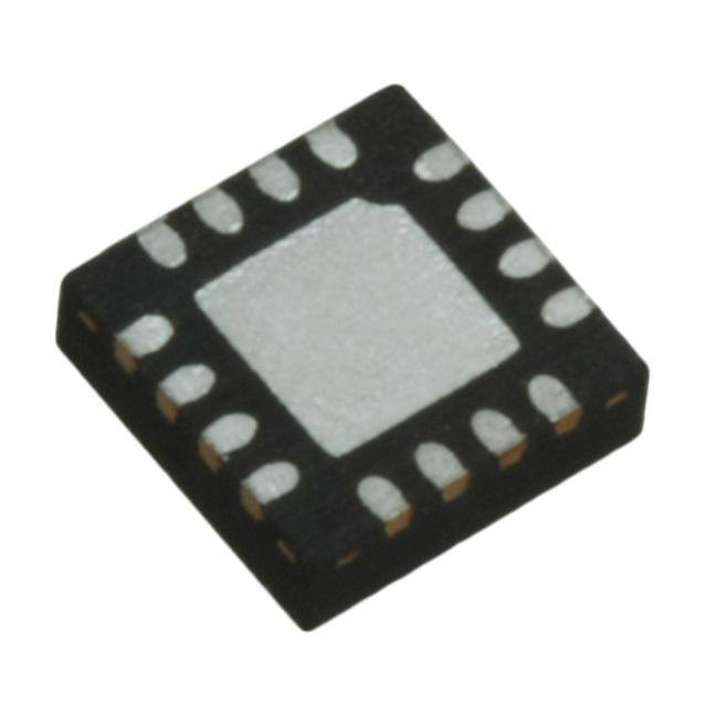
| 描述 | IC SECURITY SUPERVISOR 16-QFN |
| 产品分类 | |
| 品牌 | STMicroelectronics |
| 数据手册 | |
| 产品图片 |
|
| 产品型号 | STM1403CTNQ6F |
| rohs | 无铅 / 符合限制有害物质指令(RoHS)规范要求 |
| 产品系列 | - |
| 产品目录页面 | |
| 供应商器件封装 | 16-QFN(3x3) |
| 其它名称 | 497-8180-1 |
| 包装 | 剪切带 (CT) |
| 受监控电压数 | 1 |
| 复位 | 低有效 |
| 复位超时 | 最小为 140 ms |
| 安装类型 | 表面贴装 |
| 封装/外壳 | 16-VFQFN 裸露焊盘 |
| 工作温度 | -40°C ~ 85°C |
| 标准包装 | 1 |
| 电压-阈值 | 3.08V |
| 类型 | 简单复位/加电复位 |
| 输出 | 开路漏极或开路集电极 |
| 配用 | /product-detail/zh/STEVAL-IAS001V1/497-6398-ND/1786214/product-detail/zh/STEVAL-PCN001V1/497-5577-ND/1210610 |


PDF Datasheet 数据手册内容提取
STM1403 3 V FIPS-140 security supervisor with battery switchover Features ■ STM1403 supports FIPS-140 security level 3+ – Four high-impedance physical tamper ) inputs s ( – Over/under operating voltage detector t c – Security alarm (SAL) on tamper detection u d ■ Supervisory functions o – Automatic battery switchover r P – RST output (open drain) e – Manual (push-button) reset input (MR) t e – Power-fail comparator (PFI/PFO) QFN16, 3 mm x 3 mm (Q) l o ■ Vccsw (VCC switch output) s b – Low when switched to V CC O – High when switched to V (BATT ON BAT indicator) - ) ■ Battery low voltage detector (power-ups) ( t ■ Optional VREF (1.237 V) c u – (Available for STM1403A only) d ■ Low battery supply curroent (2.8 µA, typ) r ■ Secure low profile P16-pin, 3 x 3 mm, QFN package e t e ol s Tabble 1. Device summary O Standard Physical Over/under V Device supervisory tamper voltage (1.2R3E7F V) VOUT status, Vccsw status, functions(1) inputs alarms option during alarm during alarm STM1403A ✔ ✔ ✔ ✔ ON Normal mode(2) STM1403B(3) ✔ ✔ ✔ Note(4) High-Z High STM1403C ✔ ✔ ✔ Note(4) Ground High 1. Reset output, power-fail comparator, battery low detection (SAL, RST, PFO, and BLD are open drain). 2. Normal mode: low when V is internally switched to V and high when V is internally switched to battery. OUT CC OUT 3. Contact local ST sales office for availability. 4. Pin 9 is the V pin for STM1403A. It is the V pin for STM1403B/C. REF TPU November 2010 Doc ID 13232 Rev 6 1/34 www.st.com 1
Contents STM1403 Contents 1 Description . . . . . . . . . . . . . . . . . . . . . . . . . . . . . . . . . . . . . . . . . . . . . . . . . 6 1.1 V pin modes . . . . . . . . . . . . . . . . . . . . . . . . . . . . . . . . . . . . . . . . . . . . . 6 OUT 1.1.1 STM1403A . . . . . . . . . . . . . . . . . . . . . . . . . . . . . . . . . . . . . . . . . . . . . . . . 6 1.1.2 STM1403B . . . . . . . . . . . . . . . . . . . . . . . . . . . . . . . . . . . . . . . . . . . . . . . . 6 1.1.3 STM1403C . . . . . . . . . . . . . . . . . . . . . . . . . . . . . . . . . . . . . . . . . . . . . . . . 6 2 Pin descriptions . . . . . . . . . . . . . . . . . . . . . . . . . . . . . . . . . . . . . . . . . ). . 11 s ( 2.1 SAL, security alarm output (open drain) . . . . . . . . . . . . . . . . . . c. t. . . . . . . 11 u 2.1.1 TP1, TP3 . . . . . . . . . . . . . . . . . . . . . . . . . . . . . . . . . . . . . . . . . . . .d . . . . . . . . . . . . . . . . . .11 o 2.1.2 TP , TP 2 4 . . . . . . . . . . . . . . . . . . . . . . . . . . . . . . . . . . . . . .r . . . . . . . . . . . . . . . . . . . . . . . .11 P 2.1.3 Vccsw, V switch output . . . . . . . . . . . . . . . . . . . . . . . . . . . . . . . . . . . 11 CC e 2.1.4 BLD, VBAT low voltage detect outpute (topen drain) . . . . . . . . . . . . . . . . . 12 2.1.5 Active-low RST output (open dralin) . . . . . . . . . . . . . . . . . . . . . . . . . . . . 12 o s 2.1.6 MR, manual reset input . . . . . . . . . . . . . . . . . . . . . . . . . . . . . . . . . . . . . 12 b O 2.1.7 PFO, power-fail output (open drain) . . . . . . . . . . . . . . . . . . . . . . . . . . . . 12 2.1.8 PFI, power-fail in-put . . . . . . . . . . . . . . . . . . . . . . . . . . . . . . . . . . . . . . . . 12 ) 2.1.9 V , referesnce voltage output (1.237, typ) . . . . . . . . . . . . . . . . . . . . . . 12 REF ( t 2.1.10 V c OUT . . . . . . . . . . . . . . . . . . . . . . . . . . . . . . . . . . . . . . . . . . . . . . . . . . . . . . . . . . . . . . . . .13 u 2.1.11 dV TPU . . . . . . . . . . . . . . . . . . . . . . . . . . . . . . . . . . . . . . . . . . . . . . . . . . . . . . . . . . . . . . . . .13 o 2.1r.12 VCC . . . . . . . . . . . . . . . . . . . . . . . . . . . . . . . . . . . . . . . . . . . . . . . . . . . . . . . . . . . . . . . . . .13 P 2.1.13 V BAT . . . . . . . . . . . . . . . . . . . . . . . . . . . . . . . . . . . . . . . . . . . . . . . . . . . . . . . . . . . . . . . . . .13 e t 2.1.14 V e SS . . . . . . . . . . . . . . . . . . . . . . . . . . . . . . . . . . . . . . . . . . . . . . . . . . . . . . . . . . . . . . . . . . .13 l o 3 s Operation . . . . . . . . . . . . . . . . . . . . . . . . . . . . . . . . . . . . . . . . . . . . . . . . . 14 b O 3.1 Reset input . . . . . . . . . . . . . . . . . . . . . . . . . . . . . . . . . . . . . . . . . . . . . . . . 14 3.2 Push-button reset input . . . . . . . . . . . . . . . . . . . . . . . . . . . . . . . . . . . . . . 14 3.3 Backup battery switchover . . . . . . . . . . . . . . . . . . . . . . . . . . . . . . . . . . . . 14 3.4 Power-fail input/output . . . . . . . . . . . . . . . . . . . . . . . . . . . . . . . . . . . . . . . 15 3.5 Applications information . . . . . . . . . . . . . . . . . . . . . . . . . . . . . . . . . . . . . . 15 3.6 Negative-going V transients and undershoot . . . . . . . . . . . . . . . . . . . . 16 CC 4 Tamper detection . . . . . . . . . . . . . . . . . . . . . . . . . . . . . . . . . . . . . . . . . . . 17 4.1 Physical . . . . . . . . . . . . . . . . . . . . . . . . . . . . . . . . . . . . . . . . . . . . . . . . . . 17 2/34 Doc ID 13232 Rev 6
STM1403 Contents 4.2 Supply voltage . . . . . . . . . . . . . . . . . . . . . . . . . . . . . . . . . . . . . . . . . . . . . 17 5 Typical operating characteristics . . . . . . . . . . . . . . . . . . . . . . . . . . . . . 18 6 Maximum ratings . . . . . . . . . . . . . . . . . . . . . . . . . . . . . . . . . . . . . . . . . . . 23 7 DC and AC parameters . . . . . . . . . . . . . . . . . . . . . . . . . . . . . . . . . . . . . . 24 8 Package mechanical data . . . . . . . . . . . . . . . . . . . . . . . . . . . . . . . . . . . . 29 ) s 9 Part numbering . . . . . . . . . . . . . . . . . . . . . . . . . . . . . . . . . . . . . . . (. . . . . 31 t c u d 10 Revision history . . . . . . . . . . . . . . . . . . . . . . . . . . . . . . . . . . . . . . . . . . . 33 o r P e t e l o s b O - ) s ( t c u d o r P e t e l o s b O Doc ID 13232 Rev 6 3/34
List of tables STM1403 List of tables Table 1. Device summary. . . . . . . . . . . . . . . . . . . . . . . . . . . . . . . . . . . . . . . . . . . . . . . . . . . . . . . . . . 1 Table 2. Signal names . . . . . . . . . . . . . . . . . . . . . . . . . . . . . . . . . . . . . . . . . . . . . . . . . . . . . . . . . . . . 7 Table 3. I/O status in battery backup . . . . . . . . . . . . . . . . . . . . . . . . . . . . . . . . . . . . . . . . . . . . . . . . 15 Table 4. Absolute maximum ratings. . . . . . . . . . . . . . . . . . . . . . . . . . . . . . . . . . . . . . . . . . . . . . . . . 23 Table 5. Operating and AC measurement condition. . . . . . . . . . . . . . . . . . . . . . . . . . . . . . . . . . . . . 24 Table 6. DC and AC characteristics . . . . . . . . . . . . . . . . . . . . . . . . . . . . . . . . . . . . . . . . . . . . . . . . . 25 Table 7. Physical and environmental tamper detection levels . . . . . . . . . . . . . . . . . . . . . . . . . . . . . 28 Table 8. QFN16 – 16-lead, quad, flat package, no lead, 3 x 3 mm body size, mechanical data . . . 30 Table 9. Ordering information scheme (see Figure30 on page32 for marking information). . . . . . 31 ) Table 10. Replacement options for terminated parts . . . . . . . . . . . . . . . . . . . . . . . . . . . . . . . . .s . . . . 31 ( Table 11. Document revision history . . . . . . . . . . . . . . . . . . . . . . . . . . . . . . . . . . . . . . . . . t. . . . . . . . 33 c u d o r P e t e l o s b O - ) s ( t c u d o r P e t e l o s b O 4/34 Doc ID 13232 Rev 6
STM1403 List of figures List of figures Figure 1. Logic diagram. . . . . . . . . . . . . . . . . . . . . . . . . . . . . . . . . . . . . . . . . . . . . . . . . . . . . . . . . . . . 7 Figure 2. QFN16 connections . . . . . . . . . . . . . . . . . . . . . . . . . . . . . . . . . . . . . . . . . . . . . . . . . . . . . . . 8 Figure 3. Block diagram. . . . . . . . . . . . . . . . . . . . . . . . . . . . . . . . . . . . . . . . . . . . . . . . . . . . . . . . . . . . 8 Figure 4. Hardware hookup. . . . . . . . . . . . . . . . . . . . . . . . . . . . . . . . . . . . . . . . . . . . . . . . . . . . . . . . . 9 Figure 5. Tamper pin (TP or TP ) normally high (NH) external hookup (switch closed) . . . . . . . . . . 9 1 3 Figure 6. Tamper pin (TP or TP ) normally high (NH) external hookup (switch open). . . . . . . . . . . 10 1 3 Figure 7. Tamper pin (TP or TP ) normally low (NL) external hookup (switch closed) . . . . . . . . . . 10 2 4 Figure 8. Tamper pin (TP or TP ) normally low (NL) external hookup (switch open). . . . . . . . . . . . 10 2 4 Figure 9. Power-fail comparator waveform . . . . . . . . . . . . . . . . . . . . . . . . . . . . . . . . . . . . . . . . . . . . 16 ) Figure 10. Supply voltage protection. . . . . . . . . . . . . . . . . . . . . . . . . . . . . . . . . . . . . . . . . . . . . .s . . . . 16 ( Figure 11. V -to-V on-resistance vs. temperature . . . . . . . . . . . . . . . . . . . . . . . . . . t. . . . . . . . 18 BAT OUT c Figure 12. Supply current vs. temperature (no load). . . . . . . . . . . . . . . . . . . . . . . . . . .u . . . . . . . . . . . 18 Figure 13. V threshold vs. temperature. . . . . . . . . . . . . . . . . . . . . . . . . . . . . . . . d. . . . . . . . . . . . . . 19 PFI o Figure 14. Reset comparator propagation delay vs. temperature . . . . . . . . . . . . . . . . . . . . . . . . . . . . 19 r Figure 15. Power-up t vs. temperature . . . . . . . . . . . . . . . . . . . . . . . . . .P . . . . . . . . . . . . . . . . . . . . 19 rec Figure 16. Normalized reset threshold vs. temperature. . . . . . . . . . . . . . . . . . . . . . . . . . . . . . . . . . . . 20 e Figure 17. PFI to PFO propagation delay vs. temperature . . . . . . t. . . . . . . . . . . . . . . . . . . . . . . . . . . 20 e Figure 18. RST output voltage vs. supply voltage. . . . . . . . . . . . . . . . . . . . . . . . . . . . . . . . . . . . . . . . 20 l o Figure 19. RST response time (assertion). . . . . . . . . . . . . . . . . . . . . . . . . . . . . . . . . . . . . . . . . . . . . . 21 s Figure 20. Power-fail comparator response time (assebrtion). . . . . . . . . . . . . . . . . . . . . . . . . . . . . . . . 21 Figure 21. Power-fail comparator response time (dOe-assertion) . . . . . . . . . . . . . . . . . . . . . . . . . . . . . 21 Figure 22. V to reset propagation delay vs. t emperature. . . . . . . . . . . . . . . . . . . . . . . . . . . . . . . . . 22 CC - Figure 23. Maximum transient duration vs. reset threshold overdrive. . . . . . . . . . . . . . . . . . . . . . . . . 22 ) Figure 24. AC testing input/output wavesforms. . . . . . . . . . . . . . . . . . . . . . . . . . . . . . . . . . . . . . . . . . . 24 ( Figure 25. MR timing waveform. . .t . . . . . . . . . . . . . . . . . . . . . . . . . . . . . . . . . . . . . . . . . . . . . . . . . . . 24 c Figure 26. STM1403 switchoveur diagram, condition A (VBAT < VSW) . . . . . . . . . . . . . . . . . . . . . . . . . 24 Figure 27. STM1403 switchdover diagram, condition B (V > V ) . . . . . . . . . . . . . . . . . . . . . . . . . 24 BAT SW o Figure 28. QFN16 – 16-lead, quad, flat package, no lead, 3 x 3 mm body size, outline. . . . . . . . . . . 29 r Figure 29. QFN16 –P 16-lead, quad, flat package, no lead, 3 x 3 mm, recommended footprint. . . . . . 30 Figure 30. Tops ide marking information . . . . . . . . . . . . . . . . . . . . . . . . . . . . . . . . . . . . . . . . . . . . . . . 32 e t e l o s b O Doc ID 13232 Rev 6 5/34
Description STM1403 1 Description The STM1403 family of security supervisors are a low-power family of intrusion (tamper) detection chips targeted at manufacturers of POS terminals and other systems, to enable them to meet physical and/or environmental intrusion monitoring requirements as mandated by various standards, such as Federal Information Processing Standards (FIPS) Pub 140 entitled “Security Requirements for Cryptographic Modules,” published by the National Institute of Standards and Technology, U.S. Department of Commerce), EMVCo, ISO, ZKA, and VISA PED. STM1403 supports target levels 3 and lower. The STM1403 includes automatic battery switchover, RST output (open drain), manual (push-button) reset input (MR), power-fail comparator (PFI/PFO), physical and/or ) s environmental tamper detect/security alarm, and battery low voltage detect features. ( t The STM1403A also offers a V (1.237 V) as an option on pin 9. On the STcM1403B/C, REF u this pin is V (internally switched V or V ). TPU CC BAT d o r P 1.1 V pin modes OUT e t The STM1403 is available in three versions, correspoending to three modes of the V pin OUT (supply voltage out), when the SAL (security alaroml) is asserted (active-low) upon tamper detection: s b O 1.1.1 STM1403A - V stays ON (at V or V )) when SAL is driven low (activated). OUT CC BsAT ( t 1.1.2 STM1403B c u d V is set to High-Z when SAL is driven low (activated). OUT o r P 1.1.3 STM1403C e Vt is driven to ground when SAL is activated (may be used when V is connected e OUT OUT l directly to the V pin of the external SRAM that holds the cryptographic codes). o CC s All variants (see Table1: Device summary) are pin-compatible and available in a security- b O friendly, low profile, 16-pin QFN package. 6/34 Doc ID 13232 Rev 6
STM1403 Description Figure 1. Logic diagram V REF BLD(3) or VBATVCC V (1) TPU VCCSW(2) VOUT MR RST(3) STM1403 PFI PFO(3) TP1 (NH) SAL(3) ) s ( t TP2 TP3 TP4 VSS c (NL) (NH) (NL) u d AI09682 o 1. V only for STM1403A; V for STM1403B/C. r REF TPU P 2. Normal mode: low when V is internally switched to V and high when V is internally switched to OUT CC OUT battery. e t 3. SAL, RST, PFO, and BLD are open drain. e l o Table 2. Signal names s Vccsw(1) V switcbh output CC O MR Manual (push-button) reset input PFI -Power-fail Input ) TP - TP s Independent physical tamper detect pins 1 through 4 1 4 ( V t Supply voltage output OUT c RST(2) u Active-low reset output d PFO(2) Power-fail output o SAL(2) r Security alarm output P BLD( 2) Battery low voltage detect e tVREF(3) 1.237 V reference voltage e ol VTPU(3) Tamper pull-up (VCC or VBAT) s VBAT Backup supply voltage b V Supply voltage O CC V Ground SS 1. Normal mode: low when VOUT is internally switched to VCC and high when VOUT is internally switched to battery. 2. SAL, RST, PFO, and BLD are open drain. 3. V only for STM1403A; V for STM1403B/C. REF TPU Note: See Section2: Pin descriptions on page11 for details. Doc ID 13232 Rev 6 7/34
Description STM1403 Figure 2. QFN16 connections BLD(2)PFI VCCSW(1)VCC 16 15 14 13 RST(2) 1 12 VOUT MR 2 11 VBAT SAL(2) 3 10 PFO(2) VSS 4 5 6 7 8 9 VREF or VTPU(3) ) s TP1 TP2 TP3 TP4 ( (NH) (NL) (NH) (NL) ct AI09683 u Note: See Section2: Pin descriptions on page11 for details. d o 1. Normal mode: low when V is internally switched to V and high when Vr is internally switched to OUT CC P OUT battery. 2. SAL, RST, PFO, and BLD are open drain. e t 3. VREF only for STM1403A; VTPU for STM1403B/C e l o Figure 3. Block diagram s b VCC O VOUT BAT54J(1,2) - ) VSO COMPARE VBAT(1) s VCCSW ( t c u VINT VRST COMPARE trec (3) MR d Generator RST o PFI (3) r VPFI COMPARE PFO P t e VDET CPOOMWPEARR-EU P@ BLD(3) e (4) l VTPU o s 1.237V VREF VREF(4) b Generator O VHV COMPARE VLV COMPARE TP1 (NH) TP2 (NL) (3) TP3 (NH) SAL TP4 (NL) AI09684 1. BAT54J (from STMicroelectronics) recommended 2. Required for battery-reverse charging protection 3. Open drain 4. V only for STM1403; V for STM1403B/C REF TPU 8/34 Doc ID 13232 Rev 6
STM1403 Description Figure 4. Hardware hookup (1) Regulator VCCSW Unregulated Voltage VIN VCC VCC VOUT VCC VCC (2) 0.1µF C LPSRAM STM1403 ) R1 s ( PFIPFO(3) To Microprocessor NMtI c R2 u MR RST(3) To Microprodcessor Reset Push-Button o r BAT54J(4) P VBAT BLD(3) e To Microprocessor 1.0µF e t l o s b O TP1 From Actuator Device TP2 (3) (e.g., Switches, Wire Mesh-) SAL TP3 ) s TP4 ( ct VREF(5) To ADC u or d VTPU To Physical Tamper Pins TPX o AI09690 r P 1. Normal mode: low when V is internally switched to V and high when V is internally switched to OUT CC OUT ba ttery. e 2t. Capacitor (C) is typically ≥ 10 µF. e l 3. Open drain o s 4. Diode is required for battery reverse charge protection. b 5. V only for STM1403; V for STM1403B/C. REF TPU O Figure 5. Tamper pin (TP or TP ) normally high (NH) external hookup (switch 1 3 closed) VOUT (STM1403A) or VTPU (STM1403B/C) Switch Normally Closed; Tamper Detection on Open TP1 or TP3 R(1) AI09698 1. R typical is 10 MΩ. Resistors must be protected against conductive materials. Doc ID 13232 Rev 6 9/34
Description STM1403 Figure 6. Tamper pin (TP or TP ) normally high (NH) external hookup (switch 1 3 open) VOUT (STM1403A) or VTPU (STM1403B/C) R(1) TP1 or TP3 Switch Normally Open Tamper Detection when Closed AI10461 ) s 1. R typical is 10MΩ. Resistors must be protected against conductive materials. ( t c Figure 7. Tamper pin (TP2 or TP4) normally low (NL) external hookuup (switch closed) d o VOUT (STM1403A) P r or VTPU (STM1403B/C) e t R(1) e l o s TP2 or TP4 b O Switch Normally Closed; Tamper Detection on Open - ) s AI09699 ( 1. R typical is 10 MΩ. Resistotrs must be protected against conductive materials. c u Figure 8. Tamdper pin (TP2 or TP4) normally low (NL) external hookup (switch open) o r P VOUT (STM1403A) or e VTPU (STM1403B/C) t e Switch Normally Open; ol Tamper Detection when Closed s b TP2 or TP4 O R(1) AI10462 1. R typical is 10 MΩ. Resistors must be protected against conductive materials. 10/34 Doc ID 13232 Rev 6
STM1403 Pin descriptions 2 Pin descriptions See Figure1: Logic diagram and Table2: Signal names for a brief overview of the signals connected to this device. 2.1 SAL, security alarm output (open drain) This signal can be generated when ANY of the following conditions occur: ● V > V , where V = upper voltage trip limit (4.2 V typ); and where V = V or INT HV HV INT CC V ; BAT ) ● V < V , where V = lower voltage trip limit (2.0 V typ); and where V = Vs or INT LV LV INT (CC V ; or t BAT c ● When any of the physical tamper inputs, TP to TP , change from theiru normal states to 1 4 d the opposite (i.e., intrusion of a physical enclosure). o r Note: 1 The default state of the SAL output during initial power-up is unPdetermined. 2 The alarm function will operate either with VCC on or whene t he part is internally switched from V to V . t CC BAT e l o 2.1.1 TP1, TP3 s b O Physical tamper detect pin set normally to high (NH). They are connected externally through a closed switch or a high-impedanc-e resistor to VOUT (in the case of STM1403A) or VTPU (in the case of STM1403B/C. A ta)mper condition will be detected when the input pin is pulled s low (see Figure5 and Figure6). If not used, tie the pin to V (for STM1403A) or V (for ( OUT TPU STM1403B/C). ct u d 2.1.2 TP , TP 2 4 o r P Physical tamper detect pin set normally to low (NL). They are connected externally through a hiegh-impedance resistor or a closed switch to V . A tamper condition will be detected SS ewthen the input pin is pulled high (see Figure7 and Figure8). If not used, tie the pin to VSS. l o 2.1.s3 Vccsw, V switch output CC b O This output is low when V (see Section2.1.10: V on page13) is internally switched OUT OUT to V ; in this mode it may be used to turn on an external p-channel MOSFET switch which CC can source an external device directly from V for currents greater than 80 mA (bypassing CC the STM1403). This pin goes high when V is internally switched to V and may be used as a “BATT OUT BAT ON” indicator. If a security alarm (SAL) is issued on tamper, then the state of the Vccsw pin is as follows: Doc ID 13232 Rev 6 11/34
Pin descriptions STM1403 1. STM1403A (V remains ON when SAL is active-low): Vccsw pin will continue to OUT operate in normal mode; 2. STM1403B (V is taken to High-Z when SAL is active-low): Vccsw pin will be set to OUT high when this occurs; and 3. STM1403C (V is driven to ground when SAL is active-low): Vccsw pin will be set to OUT high when this occurs. 2.1.4 BLD, V low voltage detect output (open drain) BAT This is an internally loaded test of the battery, activated only during a power-up sequence to insure that the battery is good either prior to or after encapsulation of the module. There are three customer options for V : DET ) s ● 2.3 V (2.5 V – external diode drop of about 0.2 V) for a 3 V lithium cell ( t ● 2.5 V (2.7 V – 0.2 V) for a 3 V lithium cell or c u ● 3.2 V (3.4 V – 0.2 V) for a 3.68 V lithium “AA” battery d o This output pin will go active-low when it detects a voltage on the V pin below V . BLD rBAT DET will be released when V drops below V . P CC RST e 2.1.5 Active-low RST output (open drain) e t l o Goes low and stays low when V drops below V (reset threshold selected by the CC s RST customer), or when MR is logic low. It remaibns low for trec (200ms, typical) AFTER VCC rises above V and MR goes from low to hOigh. RST - 2.1.6 MR, manual reset input) s ( A logic low on MR assertts the RST output. The RST output remains asserted as long as MR c is low and for trec aftuer MR returns to high. This active low input has an internal 40 kΩ (typical) pull-up rdesistor. It can be driven from a TTL or CMOS logic line or shorted to ground with a switch. oLeave it open if unused. r P 2.1.7 PFeO , power-fail output (open drain) t e When PFI is less than V (power-fail input threshold voltage) or V falls below V l PFI CC SW o (battery switchover threshold ~ 2.4 V), PFO goes low, otherwise, PFO remains high. Leave s this pin open if unused. b O 2.1.8 PFI, power-fail input When PFI is less than V , or when V falls below V (see PFO, above), PFO goes PFI CC SW active-low. If this function is unused, connect this pin to V . SS 2.1.9 V , reference voltage output (1.237, typ) REF This is valid only when V is between 2.4 V and 3.6 V. When V falls below 2.4 V (V ), CC CC SW V is pulled to ground with an internal 100 kΩ resistor. This is an optional feature REF available on the STM1403A. On the STM1403B/C, this pin is V (internally switched V TPU CC or V ). If unused, this pin should float. BAT 12/34 Doc ID 13232 Rev 6
STM1403 Pin descriptions 2.1.10 V OUT This is the supply voltage output. When V rises above V (battery backup switchover CC SO voltage), V is supplied from V . In this condition, V may be connected externally to OUT CC OUT V through a p-channel MOSFET switch. When V falls below the lower value of V CC CC SW (~2.4 V), or V , V is supplied from V . It is recommended that the V pin be BAT OUT BAT OUT connected externally to a capacitor that will retain a charge for a period of time, in case an intruder forces V or V to ground. The rectifying diode connected from the positive CC BAT terminal of the battery to the V pin of the STM1403 will prevent discharge of the BAT capacitor. Three variations of parts will be offered with the following options: 1. STM1403A: V remains ON when SAL is active-low; Vccsw pin will continue to OUT ) operate in normal mode (see Section2.1.3: Vccsw, V switch output on pages11); CC ( 2. STM1403B: VOUT is taken to High-Z when SAL is active-low; Vccsw pin wctill be set to high when this occurs; and u d 3. STM1403C: VOUT is driven to ground when SAL is active-low; Voccsw pin will be set to high when this occurs. r P e 2.1.11 V TPU t e l For STM1403B and STM1403C, this pin provideso pull-up voltage for the physical tamper pins (TP1-4). This pin is not to be used as voltsage supply source for any other purpose. b Note: V is the internally switched supply voO ltage from either the V pin or the V pin. TPU CC BAT - 2.1.12 V ) CC s ( This is the supply voltacgte (2.2 V to 3.6 V). u d 2.1.13 V BAT o r P This is the secondary (backup battery) supply voltage. The pin is connected to the positive termeinal of the battery with a rectifying diode like the BAT54J from STMicroelectronics for rteverse charge protection. Voltage at this pin, after diode rectification, will be approximately e l 0.2 V less than the battery voltage, and will depend on the type of battery used as well as o s the IBAT being drawn. (A capacitor of at least 1.0 µF connected between the VBAT pin and b V is required.) If no battery is used, connect the V pin to the V pin. SS BAT CC O 2.1.14 V SS Ground, V , is the reference for the power supply. It must be connected to system ground. SS Doc ID 13232 Rev 6 13/34
Operation STM1403 3 Operation 3.1 Reset input The STM1403 security supervisor asserts a reset signal to the MCU whenever V goes CC below the reset threshold (V ), or when the push-button reset input (MR) is taken low. RST RST is guaranteed to be a logic low for 0 V < V < V if V is greater than 1 V. Without CC RST BAT a backup battery, RST is guaranteed valid down to V =1 V. CC During power-up, once V exceeds the reset threshold an internal timer keeps RST low for CC the reset time-out period, t . After this interval RST returns high. rec If V drops below the reset threshold, RST goes low. Each time RST is asserted, it s)tays CC s low for at least the reset time-out period (t ). Any time V goes below the rese(t threshold rec CC t the internal timer clears. The reset timer starts when V returns above the recset threshold. CC u d o 3.2 Push-button reset input r P A logic low on MR asserts reset. Reset remains asserted we hile MR is low, and for t (see rec Figure25 on page24) after it returns high. The MR ineptut has an internal 40 kΩ pull-up resistor, allowing it to be left open if not used. Thiso linput can be driven with TTL/CMOS-logic levels or with open-drain/collector outputs. Consnect a normally open momentary switch from b MR to ground to create a manual reset function; external debounce circuitry is not required. O If MR is driven from long cables or the device is used in a noisy environment, connect a 0.1 µF capacitor from MR to V to- provide additional noise immunity. MR may float, or be SS tied to V when not used. ) CC s ( t c u 3.3 Backup battery switchover d o In the evenrt of a power failure, it may be necessary to preserve the contents of external P SRAM through V . With a backup battery installed with voltage V , the devices OUT BAT autoematically switch the SRAM to the backup supply when V falls. CC t e Note: If backup battery is not used, connect both V and V to V . l BAT OUT CC o s This family of security supervisors does not always connect VBAT to VOUT when VBAT is b greater than V . V connects to V (through a 100 Ω switch) when V is below V CC BAT OUT CC SW O (~2.4 V) or V (whichever is lower). This is done to allow the backup battery (e.g., a 3.6 V BAT battery) to have a higher voltage than VCC. Assuming that VBAT > 2.0 V, switchover at VSO ensures that battery backup mode is entered before V gets too close to the 2.0 V minimum required to reliably retain data in most OUT external SRAMs. When V recovers, hysteresis is used to avoid oscillation around the V CC SO point. V is connected to V through a 3 Ω PMOS power switch. OUT CC Note: The backup battery may be removed while V is valid, assuming V is adequately CC BAT decoupled (0.1 µF typ), without danger of triggering a reset. 14/34 Doc ID 13232 Rev 6
STM1403 Operation Table 3. I/O status in battery backup Pin Status V Connected to V through internal switch OUT BAT V Disconnected from V CC OUT PFI Disabled PFO Logic low MR Disabled RST Logic low V Connected to V BAT OUT Vccsw Logic high ) s V Pulled to V below 2.4 V (V ) ( REF SS SW t c BLD Logic high u V Connected to V through an internal switch d TPU BAT o r P 3.4 Power-fail input/output e t e The power-fail input (PFI) is compared to an internlal reference voltage (independent from o the V comparator). If PFI is less than the power-fail threshold (V ), the power-fail RST s PFI output (PFO) will go low. This function is intbended for use as an undervoltage detector to signal a failing power supply. Typically POFI is connected through an external voltage divider (see Figure4 on page9) to either th e unregulated DC input (if it is available) or the - regulated output of the VCC reg)u lator. The voltage divider can be set up such that the s voltage at PFI falls below V several milliseconds before the regulated V input to the (PFI CC STM1403 or the microprtocessor drops below the minimum operating voltage. c u During battery backup, the power-fail comparator is turned off and PFO goes (or remains) d low (see Figuroe9 on page16). This occurs after VCC drops below VSW (~2.4V). When power returrns, the power-fail comparator is enabled and PFO follows PFI. If the comparator P is unused, PFI should be connected to V and PFO left unconnected. PFO may be SS e connected to MR so that a low voltage on PFI will generate a reset output. t e l o 3.5s Applications information b O These supervisor circuits are not short-circuit protected. Shorting V to ground - OUT excluding power-up transients such as charging a decoupling capacitor - destroys the device. Decouple both VCC and VBAT pins to ground by placing 0.1 µF capacitors as close to the device as possible. Doc ID 13232 Rev 6 15/34
Operation STM1403 Figure 9. Power-fail comparator waveform VCC VRST VSW (2.4V) trec PFO PFO follows PFI PFO follows PFI ) s ( t RST c u d AI08861a o r P 3.6 Negative-going V transients and unde rshoot CC e t The STM1403 devices are relatively immune to negateive-going V transients (glitches). l CC Figure23 on page22 was generated using a negaotive pulse applied to V , starting at V CC RST s + 0.3 V and ending below the reset threshold by the magnitude indicated (comparator b overdrive). The graph indicates the maxOimum pulse width a negative VCC transient can have without causing a reset pulse. As the magnitude of the transient increases (further below the - threshold), the maximum allowab le pulse width decreases. Any combination of duration and ) overdrive which lies under thes curve will NOT generate a reset signal. Typically, a V CC transient that goes 100 mV( below the reset threshold and lasts 40 µs or less will not cause a t c reset pulse. A 0.1 µF bypass capacitor mounted as close as possible to the V pin u CC provides additiondal transient immunity (see Figure10). o In addition to transients that are caused by normal SRAM operation, power cycling can r P generate negative voltage spikes on V that drive it to values below V by as much as CC SS onee volt. These negative spikes can cause data corruption in the SRAM while in battery btackup mode. To protect from these voltage spikes, STMicroelectronics recommends e ol connecting a Schottky diode from VCC to VSS (cathode connected to VCC, anode to VSS). s Schottky diode 1N5817 is recommended for through hole and MBRS120T3 is b recommended for surface mount. O Figure 10. Supply voltage protection VCC VCC 0.1µF DEVICE VSS AI02169 16/34 Doc ID 13232 Rev 6
STM1403 Tamper detection 4 Tamper detection 4.1 Physical There are four (4) high-impedance physical tamper detect input pins, 2 normally set to high (NH) and 2 normally set to low (NL). Each input is designed with a glitch immunity (see Table7 on page28). These inputs can be connected externally to several types of actuator devices (e.g., switches, wire mesh). A tamper on any one of the four inputs that causes its state to change will trigger the security alarm (SAL) and drive it to active-low. Once the tamper condition no longer exists, the SAL will return to its normal high state. TP and TP are set normally to high (NH). They are connected externally through a closed 1 3 ) switch or a high-impedance resistor to V (in the case of STM1403A) or V (in tshe case OUT TPU ( of STM1403B/C), A tamper condition will be detected when the input pin is pullted low (see c Figure5 and Figure6). If not used, tie the pin to V or V . u OUT TPU d TP2 and TP4 are set normally to low (NL). They are connected exteronally through a high- impedance resistor or a closed switch to V . A tamper condition rwill be detected when the SS P input pin is pulled high (see Figure7 and Figure8). If not used, tie the pin to V . SS e t e 4.2 Supply voltage ol s b The internally switched supply voltage, V (either V input or V input) is continuously O INT CC BAT monitored. If V should exceed the over voltage trip point, V (set at 4.2V, typical), or INT HV should go below the under voltage- trip point, V (set at 2.0 V, typical). SAL will be driven LV active-low. Once the tamper co)ndition no longer exists, the SAL pin will return to its normal s high state. ( t c When no tamper coundition exists, SAL is normally high (see Section2: Pin descriptions on page11). d o When a tamrper is detected, the SAL is activated (driven low), independent of the part type. P V can be driven to one of three states, depending on which variant of STM1403 is being OUT useed (see Table1: Device summary on page1): t e● ON l o ● High-Z or s b ● Ground (V ) SS O Note: The STM1403 must be initially powered above V to enable the tamper detection alarms. RST For example, if the battery is on while VCC = 0 V, no alarm condition can be detected until V rises above V (and t expires). From this point on, alarms can be detected either CC RST rec on battery or V . This is done to avoid false alarms when the device goes from no power to CC its operational state. Doc ID 13232 Rev 6 17/34
Typical operating characteristics STM1403 5 Typical operating characteristics Note: Typical values are at T = 25 °C. A Figure 11. V -to-V on-resistance vs. temperature BAT OUT ]Ω E [ 220 V = 0V C CC N 200 A T S V = 2V SI 180 BAT E N-R 160 VBAT = 3V VBAT = s3.3)V O ( T ct U140 O u V o - 120 o d - tAT 100 P r B V –60 –40 –20 0 20 40 60 80 100 120 140 TEMPERATURE [°C]e t e AI09691 l o s Figure 12. Supply current vs. temperature (no load) b O 30 - ) s 25 ( t c u d µA] 20o P ent [r 2.5V e Curr 15 3.3V y 3.6V t pl e p u l S 10 o s b O 5 0 –50 –40 –30 –20 –10 0 10 20 30 40 50 60 70 80 90 100 TEMPERATURE [°C] AI09692 18/34 Doc ID 13232 Rev 6
STM1403 Typical operating characteristics Figure 13. V threshold vs. temperature PFI 1.255 1.250 V] D [ 1.245 L V = 3.3V O CC H S 1.240 E R H T 1.235 PFI VCC = 2.5V V 1.230 ) s V = 3.0V BAT ( 1.225 ct –50 –30 –10 10 30 50 70 90 u 110 130 TEMPERATURE [°C] d o AI09693 r P Figure 14. Reset comparator propagation delay vs. teemperature t e l o µs] 24 s Y [ 22 b A O V = 3.0V EL 20 100mVB AOTVERDRIVE D - N 18 ) O s ATI 16 t( G 14 c A P u O 12 d R P o 10 r –P60 –40 –20 0 20 40 60 80 100 TEMPERATURE [°C] e AI09143 t e l o Figure 15. Power-up t vs. temperature rec s b O 215 210 s] m [c205 e tr 200 195 –50 –30 –10 10 30 50 70 90 110 130 TEMPERATURE [°C] AI09144 Doc ID 13232 Rev 6 19/34
Typical operating characteristics STM1403 Figure 16. Normalized reset threshold vs. temperature D 1.002 L O H S E 1.000 R H T T E 0.998 SV] E[ R D E 0.996 Z ALI VBAT = 3.0V M 0.994 ) R s O –60 –40 –20 0 20 40 60 80 100 12(0 140 N TEMPERATURE [°C] ct AI09145 u d Figure 17. PFI to PFO propagation delay vs. temperature o r 9 P e 8 t e µs] 7 ol AY [ 6 s L b E D 5 O N O TI 4 - A G ) A s P 3 O ( R t P 2 c u 1 d o 0r P –60 –40 –20 0 20 40 60 80 100 120 140 TEMPERATURE [°C] e AI09148 t e l Figure 18. RST output voltage vs. supply voltage o s 3.5 b O 3.0 V] E [ 2.5 G TA VCC OL 2.0 V UT VRST P 1.5 T U O ST 1.0 R 0.5 0 500 ms/div AI09149b 20/34 Doc ID 13232 Rev 6
STM1403 Typical operating characteristics Figure 19. RST response time (assertion) 4.0 3.0 VCC V] L [ E EV 2.0 L C VC VRST 1.0 ) s ( t c 0.0 u 2 µs/div d AI09151b o r Figure 20. Power-fail comparator response time (assertionP ) e 4.0 1.45 t e l o 1.40 s 3.0 b V] O 1.35 V] L [ PFO L [ E E V LEVPFO2.0 tP(FI s ) - 11..2350 V LEVPFI c 1.0 u 1.20 d o r 0.0 1.15 P 2µs/div AI09153b e t eFigure 21. Power-fail comparator response time (de-assertion) l o s 4.0 1.45 b O 3.5 1.40 3.0 EL (V)2.5 PFO 1.35 EL (V) V V E2.0 1.30 E L L V PFO1.5 PFI 1.25 V PFI 1.0 1.20 0.5 0.0 1.15 2 µs/div AI09154 Doc ID 13232 Rev 6 21/34
Typical operating characteristics STM1403 Figure 22. V to reset propagation delay vs. temperature CC 60 µs]50 Y [ A L40 E N D 10V/ms O30 1V/ms ATI 0.25V/ms G20 A P O R10 P 0 ) –60 –40 –20 0 20 40 60 80 100 s TEMPERATURE [°C] ( t AI09155 c u d Figure 23. Maximum transient duration vs. reset threshold overdrive o r P 250 e s] N [µ 200 e t O l TI o RA 150 s DU b NT 100 O E SI - TRAN 50 s ) ( 0 t 1 c 10 100 1000 10000 u d RESET COMPARATOR OVERDRIVE, VRST – VCC [mV] AI09156 o r P e t e l o s b O 22/34 Doc ID 13232 Rev 6
STM1403 Maximum ratings 6 Maximum ratings Stressing the device above the ratings listed in the absolute maximum ratings table may cause permanent damage to the device. These are stress ratings only and operation of the device at these or any other conditions above those indicated in the Operating sections of this specification is not implied. Exposure to absolute maximum rating conditions for extended periods may affect device reliability. T able 4. Absolute maximum ratings Symbol Parameter Value Unit ) TSTG Storage temperature (VCC off, VBAT off) –55 to 150 s °C ( T (1) Lead solder temperature for 10 seconds 260 t °C SLD c u V Input or output voltage –0.3 to V +0.3 V IO d CC o V /V Supply voltage –0.3 to 4.5 V CC BAT r P I Output current 20 mA O e P Power dissipation 320 mW D t e 1. Reflow at peak temperature of 255 °C to 260 °C for < 30 selconds (total thermal budget not to exceed o 180 °C for between 90 to 150 seconds). s b O - ) s ( t c u d o r P e t e l o s b O Doc ID 13232 Rev 6 23/34
DC and AC parameters STM1403 7 DC and AC parameters This section summarizes the operating measurement conditions, and the DC and AC characteristics of the device. The parameters in the DC and AC characteristics tables that follow, are derived from tests performed under the measurement conditions summarized in Table5: Operating and AC measurement condition. Designers should check that the operating conditions in their circuit match the operating conditions when relying on the quoted parameters. T able 5. Operating and AC measurement condition Parameter STM1403 U)nit s V /V supply voltage 2.2 to 3.6 ( V CC BAT t c Ambient operating temperature (T ) –40 to 85 u °C A d Input rise and fall times ≤ 5o ns r Input pulse voltages 0.2P to 0.8V V CC Input and output timing ref. voltages e 0.3 to 0.7V V CC t e l Figure 24. AC testing input/output waveformos s b 0.8VCC O 0.7VCC - 0.3VCC 0.2VCC ) AI02568 s ( t Figure 25. MR timingc waveform u d MoR r P tMLRL RST e t tMLMH trec e AI09694 l o s Figure 26. STM1403 switchover diagram, condition A (V < V ) b BAT SW O VCC = 3.3V VOUT VRST VSW =V 2B.4AVT VBAT – 75mV VBAT – 35mV AI10463 Figure 27. STM1403 switchover diagram, condition B (V > V ) BAT SW VCC = 3.3V VOUT VBAT VSW = 2.4V VSW + 40mV AI10464 24/34 Doc ID 13232 Rev 6
STM1403 DC and AC parameters Table 6. D C and AC characteristics Alter- Sym Description Test condition(1) Min Typ Max Unit native V , CC Operating voltage T = –40 to +85 °C 2.2 3.6 V V (2) A BAT V supply current CC 45 60 µA (STM1403A) Typ @ 3.3 V, 25 °C V supply current CC 30 45 µA I (STM1403B,C) CC Excluding I V supply current in OUT baCtCtery backup mode (VBAT = 2.3 V, VCC = 2.0 25 35 s )µA V, MR = V ) ( CC t c I (3) VBAT supply current in Excluding IOUT 2.8 u 4.0 µA BAT battery backup mode (V = 3.6 V) d BAT o IO(UVT1 = > 5 V mA()4) V0C.0C3 – P r V0.C0C1 5– V CC SW e V V voltage (active) IOUT1 = 80 mA tVCC – VCC – V OUT1 OUT (V > V ) e 0.3 0.15 CC SW l o IOUT1 = 250s µA, VCC – VCC – V V > Vb (4) 0.0015 0.0006 CC SW O IOUT2 = 250 µA, VBAT – VBAT – V VOUT2 VbaOcUkTu vpo)ltage (battery ( s ) -IVOUBATT2 == 12 .m2 AV, 0.1 V0B.A0T4 – V t V = 2.2 V 0.16 c BAT VTPU1 Ivnotletarngael (sawcitticvhede)d usupply ISO(UVRCE > = V 500) µA V0C.C3 – V o CC SW V InternParl switched supply ISOURCE = 100 µA VBAT – V TPU2 v oltage (battery backup) (VBAT = 2.2 V) 0.10 e t Input leakage current (MR) MR = 0 V; V = 3 V 20 75 350 µA e CC I ol Input leakage current (PFI) 0 V = VIN = VCC –25 2 +25 nA LsI Input leakage current b 0 V = V = V –1 +1 µA (TP1-TP4) IN CC O I Output leakage current 0 V = V = V (5) –1 +1 µA LO IN CC V Input high voltage (MR) 0.7V V IH CC V (max) < V < 3.6 V RST CC V Input low voltage (MR) 0.3V V IL CC V Output low voltage (PFO, VCC = VRST (max), 0.3 V OL RST, Vccsw, SAL, BLD) I = 3.2 mA SINK I = 40 µA; V = 1.0 V; OL CC V = V ; 0.3 V BAT CC VOL Output low voltage (RST) TA = 0 °C to 85 °C I = 200 µA; OL 0.3 V V = 1.2 V; V = V CC BAT CC Doc ID 13232 Rev 6 25/34
DC and AC parameters STM1403 Table 6. DC and AC characteristics (continued) Alter- Sym Description Test condition(1) Min Typ Max Unit native V V battery backup (Vccsw) I = 100 µA, 0.8V V OHB OH SOURCE BAT Pull-up supply voltage RST, SAL, BLD, PFO 3.6 V (open drain) Power-fail comparator V PFI input threshold PFI falling (V < 3.6 V) 1.212 1.237 1.262 V PFI CC PFI hysteresis PFI Rising (V < 3.6 V) 10 20 mV CC PFI to PFO propagation ) t 2 s µs PFD delay ( t c Battery switchover u d Power- VBAT > VSW oVSW V Battery backup down VBAT < VSW P r VBAT V switchover voltage (6)(7) V > V V V V Power-up BAT SW e SW SO V < V t V V BAT SWe BAT VSW ol 2.4 V s Hysteresis 40 mV b O Battery low voltage detect - M 2.25 2.30 2.34 V ) On s V Battery detect threshold power-up N 2.45 2.50 2.55 V DET ( t only c O 3.14 3.20 3.26 V u Voltage reference (option for SdTM1403A)(8) o Voltager reference 0 °C to 85 °C 1.212 1.237 1.262 V P (see Section2.1.9: V , V REF REF ereference voltage output –40 ° to 0 °C 1.200 1.237 1.274 V t (1.237, typ) on page12) e l o 0 °C to 85 °C 15 25 µA IREsF+ Source current b –40 ° to 0 °C 10 15 µA O I Sink current 10 13 µA REF– V Output voltage noise f = 100 Hz to 100 kH 10-100 µV n rms 26/34 Doc ID 13232 Rev 6
STM1403 DC and AC parameters Table 6. DC and AC characteristics (continued) Alter- Sym Description Test condition(1) Min Typ Max Unit native Reset thresholds V falling 3.00 3.075 3.15 V CC T V rising 3.00 3.085 3.17 V CC V falling 2.85 2.925 3.00 V V (9) Reset threshold S CC RST V rising 2.85 2.935 3.02 V CC V falling 2.55 2.625 2.70 V CC R ) VCC rising 2.55 2.635 2.72 s V ( t RST pulse width 140 200 t280 ms rec c u Push-button reset input d o t t MR pulse width 100 ns MLMH MR r P t t MR to RST output delay 60 500 ns MLRL MRD e 1. Valid for ambient operating temperature: T = –40 to 85 °C; V = V (max) to 3.6 V; and V = 2.8 V (except where A CC RST t BAT noted); typical values are for 3.3 V and 25 °C. e l 2. V supply current, logic input leakage, push-button reset functionality, PoFI functionality, state of RST tested at CC VBAT = 3.6 V, and VCC = 3.6 V. The state of RST and PFO is tested ast VCC = VCC (min). VBAT is voltage measured at the pin. b 3. Tested at V = 3.6 V, V = 3.5 V and 0 V. O BAT CC 4. Guaranteed by design. - 5. The leakage current measured on the RST, SAL, P)FO, and BLD pins are tested with the output not asserted (output high s impedance). ( 6. When VBAT > VCC > VSW, VOUT remainsc ctonnected to VCC until VCC drops below VSW. 7. When V > V > V , V remauins connected to V until V drops below the battery voltage (V ) – 75 mV. SW CC BAT OUT CC CC BAT d 8. Maximum external capacitiveo load on VREF pin cannot exceed 1nF. 9. The reset threshold tolerarnce is wider for V rising than for V falling due to the 10 mV (typ) hysteresis, which prevents P CC CC internal oscillation. e t e l o s b O Doc ID 13232 Rev 6 27/34
DC and AC parameters STM1403 T able 7. Physical and environmental tamper detection levels Test Sym Parameter Min Typ Max Unit conditions(1) V Overvoltage trip level 4.0 4.2 4.4 V HV V Undervoltage trip level 1.9 2.0 2.1 V LV SAL propagation delay time V + 200 mV or (after over/under voltage HV 25 50 µs V – 200 mV detection) LV Trip point for NH physical V – V – V OUT OUT V HTP tamper input pins (TP or TP ) 1.3 V(2) 0.3 V(2) 1 3 ) s Trip point for NL physical V 0.3 1.(0 V LTP tamper input pins (TP or TP ) t 2 4 c u V = SAL propagation delay time(3) HTP d V /V ; (after physical tamper pin OUT TPU o30 50 µs detection) VLTP = VSS P r V = 3.6 DD e Physical tamper input (TPX) e t 15 µs glitch immunity l o 1. Valid for ambient operating temperature: TA = –40 to s85 °C; VCC = VLV to VHV (except where noted). b 2. In the case of STM1403A, physical tamper input pins (TP ) are referenced to V (pin 12). In the case of X OUT STM1403B or C, TP are referenced to V O pin (pin 9). X TPU 3. VCC = VRST (max) to 3.6 V - ) s ( t c u d o r P e t e l o s b O 28/34 Doc ID 13232 Rev 6
STM1403 Package mechanical data 8 Package mechanical data In order to meet environmental requirements, ST offers these devices in different grades of ECOPACK® packages, depending on their level of environmental compliance. ECOPACK® specifications, grade definitions and product status are available at: www.st.com. ECOPACK® is an ST trademark. Figure 28. QFN16 – 16-lead, quad, flat package, no lead, 3 x 3 mm body size, outline D ) s ( t c u E d o r P e t e l o A3 s A b A1 O ddd C - b e ) s L K ( t c 1 u d 2 o E2 Ch r 3 P e t e ol K s D2 b QFN16-A O Note: Drawing is not to scale. Doc ID 13232 Rev 6 29/34
Package mechanical data STM1403 T able 8. QFN16 – 16-lead, quad, flat package, no lead, 3 x 3 mm body size, mechanical data mm inches Symb Typ Min Max Typ Min Max A 0.90 0.80 1.00 0.035 0.032 0.039 A1 0.02 0.00 0.05 0.001 0.000 0.002 A3 0.20 – – 0.008 – – b 0.25 0.18 0.30 0.010 0.007 0.012 D 3.00 2.90 3.10 0.118 0.114 0.122 ) s D2 1.70 1.55 1.80 0.067 0.061 (0.071 t c E 3.00 2.90 3.10 0.118 0.114 0.122 u d E2 1.70 1.55 1.80 0.067 0.061 0.071 o e 0.50 – – 0.020 r – – P K 0.20 – – 0.00 8 – – e t L 0.40 0.30 0.50 e 0.016 0.012 0.020 l ddd – 0.08 – o – 0.003 – s Ch – 0.33 b – – 0.013 – O N 16 16 - ) s Figure 29. QFN16 – 16-lead, quad, flat package, no lead, 3 x 3 mm, recommended ( footprintct u d 1.60 o r P e t 3.55 2.0 e l o s b 0.28 O AI09126 Note: Substrate pad should be tied to V . SS 30/34 Doc ID 13232 Rev 6
STM1403 Part numbering 9 Part numbering Table 9. O rdering information scheme (see Figure30 on page32 for marking information) Example: STM1403 A T M Q 6 F Device type STM1403: physical, voltage tamper detect V status (SAL = active-low) OUT A: V = ON; Vccsw = normal mode OUT B(1): V = High-Z; Vccsw = high ) OUT s C: V = ground; Vccsw = high ( OUT t c u Reset threshold voltage d T: V = 3.00 V to 3.15 V o RST r S: VRST = 2.85 V to 3.00 V P R: V = 2.55 V to 2.70 V RST e t e Battery low voltage detect threshold (VDET) ol M: VDET = 2.3 V (typ) s N: V = 2.5 V (typ) b DET O O: V = 3.2 V (typ) DET - Package ) s Q = QFN16 (3 mm x 3 mm) ( t c u Temperature range d 6 = –40 to 85 °C o r P Shipping method e F = ECOPACKt® package, tape & reel e l o 1. Csontact local ST sales office for availability. b O Note: The parts cited in Table10 are not recommended for new design. Please contact local ST sales office for availability. Table 10. R eplacement options for terminated parts Part not recommended for new design Replacement options STM1403CSMQ6F STM1403ASMQ6F or STM1403ATNQ6F or STM1403ATOQ6F STM1403CSNQ6F STM1403ASMQ6F or STM1403ATNQ6F or STM1403ATOQ6F STM1403CTNQ6F STM1403ASMQ6F or STM1403ATNQ6F or STM1403ATOQ6F For other options, or for more information on any aspect of this device, please contact the ST sales office nearest you. Doc ID 13232 Rev 6 31/34
Part numbering STM1403 Figure 30. Topside marking information 03 XXX(1) YWW (2) AI11878 1. Options codes: X = A, B, or C (for V ) OUT X = T, S, or R (for reset threshold) X = M, N, or O (for battery low voltage detect threshold) ) 2. Traceability codes s ( Y = Year t c WW = Work Week u d o r P e t e l o s b O - ) s ( t c u d o r P e t e l o s b O 32/34 Doc ID 13232 Rev 6
STM1403 Revision history 10 Revision history T able 11. Document revision history Date Revision Changes 11-Oct-2004 1 First edition Corrected footprint dimensions; update characteristics (Figure 1, 2, 26-Nov-2004 1.1 3, 4, 5, 6, 7, 8, 26, 27, 29; Table1, 2, 3, 6, 7) 22-Dec-2004 1.2 Update characteristics ( Figure4; Table6, 7, ) 03-Feb-2005 1.3 Update characteristics (Figure4; Table6, 7) ) s 25-Feb-2005 1.4 Update temperature trip limits (Table ) ( t c 06-May-2005 1.5 Update characteristics (Figure3, 4, 28; Table6, 7) u d Removed STM1404 references (Figure1, 2, 3, 4, 5, 6, 7, 8, 26, 27; 05-Aug-2005 2 o Table1, 2, 5, 6, 7, ) r P Update hardware hookup, characteristics, Lead-free text; add 18-Oct-2005 3 marking information (Figure4, 30; Taeb le6, 7, ) t e 07-Feb-2007 4 Update cover page, Table7, and part numbering (Table ). l o 20-Aug-2008 5 Minor formatting changses, updated Table1 and 7. b Added Table10O: Replacement options for terminated parts; 17-Nov-2010 6 ® updated ECOPACK text in Section8; reformatted document. - ) s ( t c u d o r P e t e l o s b O Doc ID 13232 Rev 6 33/34
STM1403 ) s Please Read Carefully: ( t c u Information in this document is provided solely in connection with ST products. STMicroelectronics NV and its subdsidiaries (“ST”) reserve the right to make changes, corrections, modifications or improvements, to this document, and the products and soervices described herein at any time, without notice. r P All ST products are sold pursuant to ST’s terms and conditions of sale. e Purchasers are solely responsible for the choice, selection and use of the ST products andt services described herein, and ST assumes no e liability whatsoever relating to the choice, selection or use of the ST products and services described herein. l o No license, express or implied, by estoppel or otherwise, to any intellectual property rights is granted under this document. If any part of this s document refers to any third party products or services it shall not be deemed a license grant by ST for the use of such third party products b or services, or any intellectual property contained therein or considered as a warranty covering the use in any manner whatsoever of such O third party products or services or any intellectual property contained therein. - ) UNLESS OTHERWISE SET FORTH IN ST’S TERMSs AND CONDITIONS OF SALE ST DISCLAIMS ANY EXPRESS OR IMPLIED WARRANTY WITH RESPECT TO THE USE AN(D/OR SALE OF ST PRODUCTS INCLUDING WITHOUT LIMITATION IMPLIED t WARRANTIES OF MERCHANTABILITY, FITNcESS FOR A PARTICULAR PURPOSE (AND THEIR EQUIVALENTS UNDER THE LAWS OF ANY JURISDICTION), OR INFRINGEMuENT OF ANY PATENT, COPYRIGHT OR OTHER INTELLECTUAL PROPERTY RIGHT. d UNLESS EXPRESSLY APPROVED IN WRITING BY AN AUTHORIZED ST REPRESENTATIVE, ST PRODUCTS ARE NOT o RECOMMENDED, AUTHORIZED OR WARRANTED FOR USE IN MILITARY, AIR CRAFT, SPACE, LIFE SAVING, OR LIFE SUSTAINING r APPLICATIONS, NOR IN PPRODUCTS OR SYSTEMS WHERE FAILURE OR MALFUNCTION MAY RESULT IN PERSONAL INJURY, DEATH, OR SEVERE P ROPERTY OR ENVIRONMENTAL DAMAGE. ST PRODUCTS WHICH ARE NOT SPECIFIED AS "AUTOMOTIVE GRADE" MAY ONLYe BE USED IN AUTOMOTIVE APPLICATIONS AT USER’S OWN RISK. t e l o Resale of ST products with provisions different from the statements and/or technical features set forth in this document shall immediately void s any warranty granted by ST for the ST product or service described herein and shall not create or extend in any manner whatsoever, any b liability of ST. O ST and the ST logo are trademarks or registered trademarks of ST in various countries. Information in this document supersedes and replaces all information previously supplied. The ST logo is a registered trademark of STMicroelectronics. All other names are the property of their respective owners. © 2010 STMicroelectronics - All rights reserved STMicroelectronics group of companies Australia - Belgium - Brazil - Canada - China - Czech Republic - Finland - France - Germany - Hong Kong - India - Israel - Italy - Japan - Malaysia - Malta - Morocco - Philippines - Singapore - Spain - Sweden - Switzerland - United Kingdom - United States of America www.st.com 34/34 Doc ID 13232 Rev 6