ICGOO在线商城 > STM1061N21WX6F
 Datasheet下载
- 型号: STM1061N21WX6F
- 制造商: STMicroelectronics
- 库位|库存: xxxx|xxxx
- 要求:
| 数量阶梯 | 香港交货 | 国内含税 |
| +xxxx | $xxxx | ¥xxxx |
查看当月历史价格
查看今年历史价格
STM1061N21WX6F产品简介:
ICGOO电子元器件商城为您提供STM1061N21WX6F由STMicroelectronics设计生产,在icgoo商城现货销售,并且可以通过原厂、代理商等渠道进行代购。 提供STM1061N21WX6F价格参考以及STMicroelectronicsSTM1061N21WX6F封装/规格参数等产品信息。 你可以下载STM1061N21WX6F参考资料、Datasheet数据手册功能说明书, 资料中有STM1061N21WX6F详细功能的应用电路图电压和使用方法及教程。
| 参数 | 数值 |
| 产品目录 | 集成电路 (IC)半导体 |
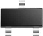
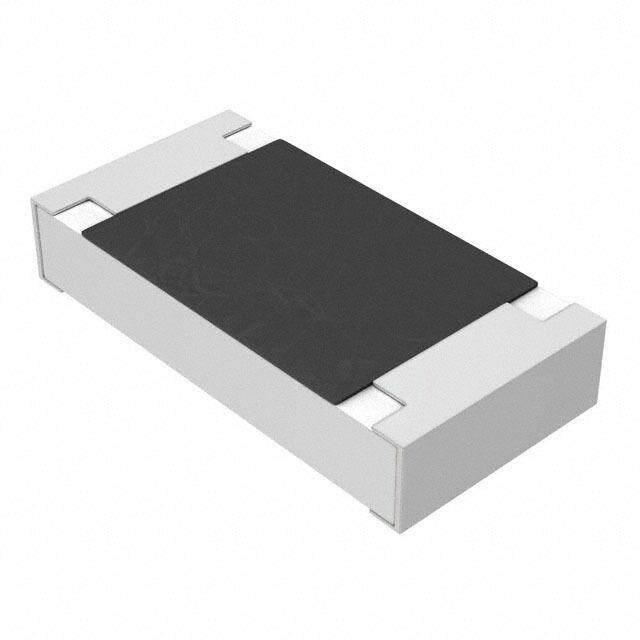
| 描述 | IC VOLT DETECTOR LP 2.1V SOT-23监控电路 Lo Pwr Vltg Detector |
| 产品分类 | |
| 品牌 | STMicroelectronics |
| 产品手册 | |
| 产品图片 |
|
| rohs | 符合RoHS无铅 / 符合限制有害物质指令(RoHS)规范要求 |
| 产品系列 | 电源管理 IC,监控电路,STMicroelectronics STM1061N21WX6F- |
| NumberofInputsMonitored | 1 Input |
| 数据手册 | |
| 产品型号 | STM1061N21WX6F |
| 产品目录页面 | |
| 产品种类 | 监控电路 |
| 人工复位 | No Manual Reset |
| 供应商器件封装 | SOT-23-3 |
| 其它名称 | 497-7492-6 |
| 其它有关文件 | http://www.st.com/web/catalog/sense_power/FM1946/SC665/PF89794?referrer=70071840 |
| 功率失效检测 | No |
| 包装 | Digi-Reel® |
| 受监控电压数 | 1 |
| 商标 | STMicroelectronics |
| 复位 | 低有效 |
| 复位超时 | 标准传输延迟为 30 µs |
| 安装类型 | 表面贴装 |
| 安装风格 | SMD/SMT |
| 封装 | Reel |
| 封装/外壳 | TO-236-3,SC-59,SOT-23-3 |
| 封装/箱体 | SOT-23-3 |
| 工作温度 | -40°C ~ 85°C |
| 工作电源电流 | 3.6 uA |
| 工厂包装数量 | 3000 |
| 最大功率耗散 | 320 mW |
| 最大工作温度 | + 85 C |
| 最小工作温度 | - 40 C |
| 标准包装 | 1 |
| 欠电压阈值 | 2.058 V |
| 电压-阈值 | 2.1V |
| 电池备用开关 | No Backup |
| 电源电压-最大 | 6 V |
| 电源电压-最小 | 0.7 V |
| 监视器 | No Watchdog |
| 类型 | 简单复位/加电复位 |
| 系列 | STM1061 |
| 芯片启用信号 | No Chip Enable |
| 被监测输入数 | 1 Input |
| 输出 | 开路漏极或开路集电极 |
| 输出类型 | Active Low, Open Drain |
| 过电压阈值 | 2.142 V |
| 阈值电压 | 2.1 V |


- 商务部:美国ITC正式对集成电路等产品启动337调查
- 曝三星4nm工艺存在良率问题 高通将骁龙8 Gen1或转产台积电
- 太阳诱电将投资9.5亿元在常州建新厂生产MLCC 预计2023年完工
- 英特尔发布欧洲新工厂建设计划 深化IDM 2.0 战略
- 台积电先进制程称霸业界 有大客户加持明年业绩稳了
- 达到5530亿美元!SIA预计今年全球半导体销售额将创下新高
- 英特尔拟将自动驾驶子公司Mobileye上市 估值或超500亿美元
- 三星加码芯片和SET,合并消费电子和移动部门,撤换高东真等 CEO
- 三星电子宣布重大人事变动 还合并消费电子和移动部门
- 海关总署:前11个月进口集成电路产品价值2.52万亿元 增长14.8%


PDF Datasheet 数据手册内容提取
STM1061 Low Power Voltage Detector Features Figure 1. Packages ■ Factory-trimmed Voltage Thresholds in 0.1V Increments from 1.6 to 5.5V ■ ±2% Voltage Threshold Accuracy ■ Operating Voltage 0.7 to 6.0V ■ Open Drain Output SOT23-3 (WX) ■ Low Supply Current of 0.9µA (typ) ■ Guaranteed OUT Assertion Down to V = 0.7V CC ■ Power Supply Transient Immunity ■ Available in SOT23-3 and SOT323-3 (SC70-3) packages SOT323-3, SC70-3 (W) (1) ■ Operating Temperature –40 to 85°C. 1. Contact local sales office for availability. July 2006 Rev 4 1/23 www.st.com 1
Contents STM1061 Contents 1 Summary Description . . . . . . . . . . . . . . . . . . . . . . . . . . . . . . . . . . . . . . . . 5 2 Pin Descriptions . . . . . . . . . . . . . . . . . . . . . . . . . . . . . . . . . . . . . . . . . . . . 7 2.1 OUT (Open Drain) . . . . . . . . . . . . . . . . . . . . . . . . . . . . . . . . . . . . . . . . . . . 7 2.2 V . . . . . . . . . . . . . . . . . . . . . . . . . . . . . . . . . . . . . . . . . . . . . . . . . . . . . . . 7 CC 2.3 V . . . . . . . . . . . . . . . . . . . . . . . . . . . . . . . . . . . . . . . . . . . . . . . . . . . . . . . 7 SS 3 Operation . . . . . . . . . . . . . . . . . . . . . . . . . . . . . . . . . . . . . . . . . . . . . . . . . . 8 3.1 Output . . . . . . . . . . . . . . . . . . . . . . . . . . . . . . . . . . . . . . . . . . . . . . . . . . . . 8 3.2 Negative-Going V Transients and Undershoot . . . . . . . . . . . . . . . . . . . . 8 CC 4 Typical Operating Characteristics . . . . . . . . . . . . . . . . . . . . . . . . . . . . . . 9 5 Maximum Rating . . . . . . . . . . . . . . . . . . . . . . . . . . . . . . . . . . . . . . . . . . . 13 6 DC and AC Parameters . . . . . . . . . . . . . . . . . . . . . . . . . . . . . . . . . . . . . . 14 7 Package Mechanical . . . . . . . . . . . . . . . . . . . . . . . . . . . . . . . . . . . . . . . . 17 8 Part Numbering . . . . . . . . . . . . . . . . . . . . . . . . . . . . . . . . . . . . . . . . . . . . 20 9 Revision History . . . . . . . . . . . . . . . . . . . . . . . . . . . . . . . . . . . . . . . . . . . 22 2/23
STM1061 List of tables List of tables Table 1. Signal Names . . . . . . . . . . . . . . . . . . . . . . . . . . . . . . . . . . . . . . . . . . . . . . . . . . . . . . . . . . . . 5 Table 2. Pin Functions . . . . . . . . . . . . . . . . . . . . . . . . . . . . . . . . . . . . . . . . . . . . . . . . . . . . . . . . . . . . 7 Table 3. Absolute Maximum Ratings . . . . . . . . . . . . . . . . . . . . . . . . . . . . . . . . . . . . . . . . . . . . . . . . 13 Table 4. Operating and AC Measurement Conditions . . . . . . . . . . . . . . . . . . . . . . . . . . . . . . . . . . . 14 Table 5. DC and AC Characteristics. . . . . . . . . . . . . . . . . . . . . . . . . . . . . . . . . . . . . . . . . . . . . . . . . 16 Table 6. SOT23-3 – 3-lead Small Outline Transistor Package Mechanical Data. . . . . . . . . . . . . . . 18 Table 7. SOT323-3 (SC70-3) – 3-lead Small Outline Transistor Package Mechanical Data . . . . . . 19 Table 8. Ordering Information Scheme. . . . . . . . . . . . . . . . . . . . . . . . . . . . . . . . . . . . . . . . . . . . . . . 20 Table 9. Factory-Trimmed Thresholds with Marking Description . . . . . . . . . . . . . . . . . . . . . . . . . . . 21 Table 10. Document Revision History . . . . . . . . . . . . . . . . . . . . . . . . . . . . . . . . . . . . . . . . . . . . . . . . 22 3/23
List of figures STM1061 List of figures Figure 1. Packages . . . . . . . . . . . . . . . . . . . . . . . . . . . . . . . . . . . . . . . . . . . . . . . . . . . . . . . . . . . . . . . 1 Figure 2. Logic Diagram. . . . . . . . . . . . . . . . . . . . . . . . . . . . . . . . . . . . . . . . . . . . . . . . . . . . . . . . . . . . 5 Figure 3. SOT23-3 Connections . . . . . . . . . . . . . . . . . . . . . . . . . . . . . . . . . . . . . . . . . . . . . . . . . . . . . 5 Figure 4. SOT323-3 (SC70-3) Connections. . . . . . . . . . . . . . . . . . . . . . . . . . . . . . . . . . . . . . . . . . . . . 6 Figure 5. N-Channel Open Drain Output Block Diagram. . . . . . . . . . . . . . . . . . . . . . . . . . . . . . . . . . . 6 Figure 6. STM1061N Active-Low, Open Drain Hardware Hookup. . . . . . . . . . . . . . . . . . . . . . . . . . . . 6 Figure 7. Supply Current vs. Input Voltage . . . . . . . . . . . . . . . . . . . . . . . . . . . . . . . . . . . . . . . . . . . . . 9 Figure 8. Supply Current vs. Ambient Temperature . . . . . . . . . . . . . . . . . . . . . . . . . . . . . . . . . . . . . . 9 Figure 9. Output Detect Delay Time vs. Ambient Temperature. . . . . . . . . . . . . . . . . . . . . . . . . . . . . 10 Figure 10. Output Release Delay Time vs. Ambient Temperature . . . . . . . . . . . . . . . . . . . . . . . . . . . 10 Figure 11. Maximum Transient Duration vs. Reset Threshold Overdrive . . . . . . . . . . . . . . . . . . . . . . 11 Figure 12. Detect, Release Voltage vs. Ambient Temperature for V = 3.4V . . . . . . . . . . . . . . . . . 11 TH– Figure 13. N-channel Driver Output Current vs. V DS . . . . . . . . . . . . . . . . . . . . . . . . . . . . . . . . . . . . . . . . . . . . . . . .12 Figure 14. N-channel Driver Output Current vs. Input Voltage for V = 0.5V . . . . . . . . . . . . . . . . . . 12 DS Figure 15. AC Testing Input/Output Waveforms . . . . . . . . . . . . . . . . . . . . . . . . . . . . . . . . . . . . . . . . . 14 Figure 16. Voltage Timing Waveform . . . . . . . . . . . . . . . . . . . . . . . . . . . . . . . . . . . . . . . . . . . . . . . . . 15 Figure 17. SOT23-3 – 3-lead Small Outline Transistor Package Outline. . . . . . . . . . . . . . . . . . . . . . . 17 Figure 18. SOT323-3 (SC70-3) – 3-lead Small Outline Transistor Package Outline. . . . . . . . . . . . . . 19 4/23
STM1061 Summary Description 1 Summary Description The STM1061 low power voltage detector provides monitoring of battery, power-supply, and regulated system voltages. A precision voltage reference and comparator monitors the V CC input and compares it with a specified voltage threshold condition. When V falls below a CC specified trip point threshold, the output (OUT) is forced low and remains asserted as long as the V input remains below V + hysteresis (V ). The STM1061 device is CC TH– HYST guaranteed to output the correct logic state for V down to 0.7V. They are also designed to CC ignore fast transients on V . CC This small, low power device is ideal for portable applications and is available in space- saving SOT23-3 and SOT323-3 (SC70-3) packages. Figure 2. Logic Diagram V CC STM1061 OUT V SS AI10477 Table 1. Signal Names OUT Open Drain Active-Low Output V Supply Voltage CC V Ground SS Figure 3. SOT23-3 Connections OUT 1 3 VCC VSS 2 AI10478 5/23
Summary Description STM1061 Figure 4. SOT323-3 (SC70-3) Connections VSS 1 3 VCC OUT 2 AI10479 Figure 5. N-Channel Open Drain Output Block Diagram VCC OUT R1 + – R2 VREF VSS R3 AI10482 Figure 6. STM1061N Active-Low, Open Drain Hardware Hookup DC/DC Converter Regulated 3V VIN VOUT VSS R VCC + 3.6V STM1061N MCU (Open Drain) VOUT VCC OUT Suspend VSS VSS AI10484a 6/23
STM1061 Pin Descriptions 2 Pin Descriptions See Figure2 on page5 and Table1 on page5 for a brief overview of the signals connected to this device. 2.1 OUT (Open Drain) This is the Open Drain Output. It goes low when V drops below V , and remains low as CC TH– long as V is below V + V . CC TH– HYST 2.2 V CC This is the Supply voltage and input for the Voltage Detector. 2.3 V SS Ground, V , is the reference for the power supply. It must be connected to the system SS ground. Table 2. Pin Functions Pin Name Function SOT323-3 SOT23-3 (SC70-3) 1 2 OUT Active-Low Open Drain Output 3 3 V Supply Voltage CC 2 1 V Ground SS 7/23
Operation STM1061 3 Operation 3.1 Output The STM1061 Voltage Detector monitors system voltages from 1.6 to 5V in 100mV increments. The detector is designed to ignore fast transients on V and has a voltage CC hysteresis (V ). The STM1061 asserts an output signal (OUT) whenever V goes HYST CC below the Voltage Detect Threshold (V ). The output signal (OUT) stays asserted until TH– V goes above the Voltage Detect Release (V ). Output voltage (V ) is guaranteed CC TH+ OUT valid down to V =0.7V at 25°C. CC The STM1061has an open drain active-low output which will sink current when output is asserted. Connect a pull-up resistor from OUT to any supply voltage up to 6V (see Figure6 on page6). Select a resistor value large enough to register a logic low, and small enough to register a logic high while all of the input current and leakage paths connected to the reset output line are being supplied. A 10k pull-up is sufficient in most applications. The advantages of open drain output is the ability to connect more open drain outputs in parallel (wired OR connections) as well as connect the output to a power supply voltage different from V . CC 3.2 Negative-Going V Transients and Undershoot CC The STM1061 device is relatively immune to negative-going V transients (glitches). The CC graph (see Figure11 on page11) indicates the maximum pulse width a negative V CC transient can have without causing a reset pulse. As the magnitude of the transient increases (further below the threshold), the maximum allowable pulse width decreases. Any combination of duration and overdrive which lies under the curve will NOT generate a reset signal. A 0.1µF bypass capacitor mounted as close as possible to the V pin provides additional CC transient immunity. 8/23
STM1061 Typical Operating Characteristics 4 Typical Operating Characteristics Figure 7. Supply Current vs. Input Voltage 1400 1200 1000 A) 800 n (C C600 I Temp = –40°C 400 Temp = 25°C 200 Temp = 85°C 0 0 1 2 3 4 5 6 VCC (V) AI11119b Figure 8. Supply Current vs. Ambient Temperature 1250 1000 A) n (C C nt: I 750 e r r Cu 500 VCC = 5V y VCC = 3V ppl VCC = 2V u S 250 0 -40 -20 0 20 40 60 80 Ambient Temperature (°C) AI11120b 9/23
Typical Operating Characteristics STM1061 Figure 9. Output Detect Delay Time vs. Ambient Temperature 35.00 s) 30.00 µ (D y: tP25.00 VTH– = 3.4V a el D 20.00 ct e Det 15.00 T U o-O 10.00 VTH– = 1.6V -tC C 5.00 V 0.00 –40 –20 0 20 40 60 80 Ambient Temperature: TA (°C) AI11121b Figure 10. Output Release Delay Time vs. Ambient Temperature 50.00 45.00 µs) 40.00 (R VTH+ = 3.57V y: tP35.00 a el 30.00 D e as 25.00 e el T R 20.00 U O o- 15.00 -tC VTH+ = 1.68V C10.00 V 5.00 0.00 –40 –20 0 20 40 60 80 Ambient Temperature: TA (°C) AI11122b 10/23
STM1061 Typical Operating Characteristics Figure 11. Maximum Transient Duration vs. Reset Threshold Overdrive 160 140 s) 120 VTH– = 3.4V n (µ VTH– = 1.6V o 100 ati r u 80 D nt e 60 si n Tra 40 20 0 1 10 100 1000 10000 Threshold Overdrive (mV) AI11123b 1. Reset occurs above the curve. Figure 12. Detect, Release Voltage vs. Ambient Temperature for V = 3.4V TH– 3.6 V) (+ H T V , – H T 3.5 V e: ag Detect Voltage, VTH– olt Release Voltage, VTH+ V e s a 3.4 e el R ct, e et D 3.3 –40 –20 0 20 40 60 80 Ambient Temperature (°C) AI11124b 11/23
Typical Operating Characteristics STM1061 Figure 13. N-channel Driver Output Current vs. V DS 0.06 VCC = 3.3V 0.05 VCC = 3.0V A) VCC = 2.7V nt: I (D 0.04 VVCCCC == 21..15VV e r 0.03 ur VCC = 1.0V C ut p 0.02 ut O 0.01 0 0 0.25 0.5 0.75 1 1.25 1.5 Output Voltage: VDS (V) AI11125b Figure 14. N-channel Driver Output Current vs. Input Voltage for V = 0.5V DS 30 25 A) m Temp. (25°C) (T 20 Temp. (85°C) U O Temp. (–40°C) nt: I 15 e r r u C ut 10 p ut O 5 0 0 0.5 1 1.5 2 2.5 3 Input Voltage: VCC (V) AI11126b 12/23
STM1061 Maximum Rating 5 Maximum Rating Stressing the device above the rating listed in the Table3: Absolute Maximum Ratings may cause permanent damage to the device. These are stress ratings only and operation of the device at these or any other conditions above those indicated in the Operating sections of this specification is not implied. Exposure to Absolute Maximum Rating conditions for extended periods may affect device reliability. Refer also to the STMicroelectronics SURE Program and other relevant quality documents. Table 3. Absolute Maximum Ratings Symbol Parameter Value Unit T Storage Temperature (V Off, V Off) –55 to 150 °C STG CC BAT T (1) Lead Solder Temperature for 10 seconds 260 °C SLD V Input or Output Voltage –0.3 to V +0.3 V IO CC V Supply Voltage –0.3 to 7.0 V CC I Output Current 20 mA O P Power Dissipation 320 mW D 1. Reflow at peak temperature of 260°C (total thermal budget not to exceed 245°C for greater than 30 seconds). 13/23
DC and AC Parameters STM1061 6 DC and AC Parameters This section summarizes the operating measurement conditions, and the DC and AC characteristics of the device. The parameters in the DC and AC characteristics Tables that follow, are derived from tests performed under the Measurement Conditions summarized in Table4: Operating and AC Measurement Conditions. Designers should check that the operating conditions in their circuit match the operating conditions when relying on the quoted parameters. T able 4. Operating and AC Measurement Conditions Sym Parameter STM1061 Unit V Supply Voltage 0.7 to 6.0 V CC T Ambient Operating Temperature –40 to 85 °C A Input Rise and Fall Times ≤ 05 ns Input Pulse Voltages 0.2 to 0.8V V CC Input and Output Timing Ref. Voltages 0.3 to 0.7V V CC Figure 15. AC Testing Input/Output Waveforms 0.8VCC 0.7VCC 0.3VCC 0.2VCC AI02568 14/23
STM1061 DC and AC Parameters Figure 16. Voltage Timing Waveform VCC VTH+ Release Voltage (VTH+ = VTH– + VHYST) VTH– Detect Voltage VCC (min) VSS VOUT tPD tPR Detect Delay Release Delay VSS AI10483 15/23
DC and AC Parameters STM1061 Table 5. DC and AC Characteristics Sym. Description Test Condition (1) Min Typ Max Unit V Operating Voltage 0.7 6.0 V CC V = 3.0V, No Load 0.9 3.0 µA CC I V Supply Current CC CC V = 5.5V, No Load 1.1 3.6 µA CC V = 1.0V 1.0 1.7 mA CC Output Current, N-channel VCC = 2.0V 3.0 14 mA I (V = 0.5V), V = 3.0V 5.0 22 mA OUT DS CC Reset asserted V = 4.0V 6.0 26 mA CC V = 5.0V 7.0 30 mA CC Voltage Thresholds Detect Voltage (2) VTH– (see Table9 on page21 for VTH– – 2% VTH– VTH– + 2% V detailed listing) V + V Release Voltage TH– V TH+ V HYST VHYST Threshold Hysteresis 0.02VTH– 0.05VTH– 0.08VTH– V V falling from (V CC TH– + 100mV) to (V – t V to OUT Detect Delay TH– 25 µs PD CC 100mV) at 10mV/µs V rising from (V CC TH+ – 100mV) to (V + t V to OUT Release Delay TH+ 30 200 µs PR CC 100mV) at 10mV/µs Threshold Temperature ±100 ppm/oC Coefficient 1. Valid for Ambient Operating Temperature: T = 25°C. A 2. Other V threshold are offered. Minimum order quantities may apply. Contact local sales office for availability. TH- 16/23
STM1061 Package Mechanical 7 Package Mechanical In order to meet environmental requirements, ST offers these devices in ECOPACK® packages. These packages have a Lead-free second level interconnect. The category of second Level Interconnect is marked on the package and on the inner box label, in compliance with JEDEC Standard JESD97. The maximum ratings related to soldering conditions are also marked on the inner box label. ECOPACK is an ST trademark. ECOPACK specifications are available at: www.st.com. Figure 17. SOT23-3 – 3-lead Small Outline Transistor Package Outline E E1 B 0.15 M CAB A1 1 e e1 D 3X 0.20 M CAB A 0.10 C A2 3X b C A C θ L1 C L SOT23-3 1. Drawing is not to scale. 17/23
Package Mechanical STM1061 Table 6. SOT23-3 – 3-lead Small Outline Transistor Package Mechanical Data mm inches Symbol Typ Min Max Typ Min Max A 0.89 1.12 0.035 0.044 A1 0.01 0.10 0.001 0.004 A2 0.88 1.02 0.035 0.042 b 0.30 0.50 0.012 0.020 C 0.08 0.20 0.003 0.008 D 2.80 3.04 0.110 0.120 E 2.10 2.64 0.083 0.104 E1 1.20 1.40 0.047 0.055 e 0.89 1.03 0.035 0.041 e1 1.78 2.05 0.070 0.081 L 0.54 0.021 L1 0.40 0.60 0.016 0.024 Q 0° 8° 0° 8° N 3 3 18/23
STM1061 Package Mechanical Figure 18. SOT323-3 (SC70-3) – 3-lead Small Outline Transistor Package Outline E E1 B 0.30 M CAB A1 1 e e1 D 3X 0.10 M CAB A 0.10 C A2 3X b C θ1 A C θ L1 C L SOT323-3 1. Drawing is not to scale. Table 7. SOT323-3 (SC70-3) – 3-lead Small Outline Transistor Package Mechanical Data mm inches Symbol Typ Min Max Typ Min Max A 0.80 1.10 0.031 0.043 A1 0.00 0.10 0.000 0.004 A2 0.80 1.00 0.031 0.039 b 0.25 0.40 0.010 0.016 C 0.10 0.18 0.004 0.007 D 1.80 2.20 0.071 0.087 E 1.80 2.40 0.071 0.094 E1 1.15 1.35 0.045 0.053 e 0.65 0.026 e1 1.30 0.051 L 0.35 0.45 0.014 0.018 L1 0.10 0.30 0.004 0.012 Q 0° 30° 0° 30° Θ1 8° 12° 8° 12° N 3 3 19/23
Part Numbering STM1061 8 Part Numbering Table 8. Ordering Information Scheme Example: STM1061 N xx WX 6 F Device Type STM1061 Output Type N = Open Drain (Active-Low) Threshold Voltage (1) xx = See Table9 on page21 Package WX = SOT23-3 W = SOT323-3 (SC70-3) (1) Temperature Range 6 = –40 to 85°C Shipping Method F = ECOPACK Package, Tape & Reel 1. Other thresholds voltage options are offered. Minimum order quantities may apply. Contact local sales office for availability. For other options, or for more information on any aspect of this device, please contact the ST Sales Office nearest you. 20/23
STM1061 Part Numbering T able 9. Factory-Trimmed Thresholds with Marking Description Threshold Voltage V (V) at T = 25°C (1) TH– A Suffix Topside Marking Min (–2%) Typ Max (+2%) 16 1.568 1.600 1.632 16Nx 17 1.666 1.700 1.734 17Nx 19 1.862 1.900 1.938 19Nx 21 2.058 2.100 2.142 21Nx 22 2.156 2.200 2.244 22Nx 23 2.254 2.300 2.346 23Nx 25 2.450 2.500 2.550 25Nx 26 2.548 2.600 2.652 26Nx 27 2.646 2.700 2.754 27Nx 28 2.744 2.800 2.856 28Nx 29 2.842 2.900 2.958 29Nx 30 2.940 3.000 3.060 30Nx 31 3.038 3.100 3.162 31Nx 34 3.332 3.400 3.468 34Nx 38 3.724 3.800 3.876 38Nx 1. Other V thresholds are offered. Minimum order quantities may apply. Contact local sales office for TH- availability. 21/23
Revision History STM1061 9 Revision History Table 10. Document Revision History Date Version Description 20-January- 1.0 First Edition 2004 Update Operation section, characteristics; insert new graphics; add 01-Aug-05 1.1 ECOPACK information ( Figure7, 8, 9, 10, 11, 12, 13, and 14; Table Table5, 8, and 9) Update characteristics, remove ‘push-pull output’ reference (Figure8, 02-Sep-05 1.2 9, 10, 11, 12, and 16; Table Table2, , 5, and 8) Status upgrade; update characteristics; add Marking information 19-Oct-05 2.0 (Figure7, 8, 9, 10, 11, 12, 13, and 14; Table Table8, and 9) 18-Nov-05 3.0 Update characteristics (Table3, and 4) 27-Jul-2006 4 Update Chapter: Features, Figure1, 5, 6, Table8 and 9. 22/23
STM1061 Please Read Carefully: Information in this document is provided solely in connection with ST products. STMicroelectronics NV and its subsidiaries (“ST”) reserve the right to make changes, corrections, modifications or improvements, to this document, and the products and services described herein at any time, without notice. All ST products are sold pursuant to ST’s terms and conditions of sale. Purchasers are solely responsible for the choice, selection and use of the ST products and services described herein, and ST assumes no liability whatsoever relating to the choice, selection or use of the ST products and services described herein. No license, express or implied, by estoppel or otherwise, to any intellectual property rights is granted under this document. If any part of this document refers to any third party products or services it shall not be deemed a license grant by ST for the use of such third party products or services, or any intellectual property contained therein or considered as a warranty covering the use in any manner whatsoever of such third party products or services or any intellectual property contained therein. UNLESS OTHERWISE SET FORTH IN ST’S TERMS AND CONDITIONS OF SALE ST DISCLAIMS ANY EXPRESS OR IMPLIED WARRANTY WITH RESPECT TO THE USE AND/OR SALE OF ST PRODUCTS INCLUDING WITHOUT LIMITATION IMPLIED WARRANTIES OF MERCHANTABILITY, FITNESS FOR A PARTICULAR PURPOSE (AND THEIR EQUIVALENTS UNDER THE LAWS OF ANY JURISDICTION), OR INFRINGEMENT OF ANY PATENT, COPYRIGHT OR OTHER INTELLECTUAL PROPERTY RIGHT. UNLESS EXPRESSLY APPROVED IN WRITING BY AN AUTHORIZED ST REPRESENTATIVE, ST PRODUCTS ARE NOT RECOMMENDED, AUTHORIZED OR WARRANTED FOR USE IN MILITARY, AIR CRAFT, SPACE, LIFE SAVING, OR LIFE SUSTAINING APPLICATIONS, NOR IN PRODUCTS OR SYSTEMS WHERE FAILURE OR MALFUNCTION MAY RESULT IN PERSONAL INJURY, DEATH, OR SEVERE PROPERTY OR ENVIRONMENTAL DAMAGE. ST PRODUCTS WHICH ARE NOT SPECIFIED AS "AUTOMOTIVE GRADE" MAY ONLY BE USED IN AUTOMOTIVE APPLICATIONS AT USER’S OWN RISK. Resale of ST products with provisions different from the statements and/or technical features set forth in this document shall immediately void any warranty granted by ST for the ST product or service described herein and shall not create or extend in any manner whatsoever, any liability of ST. ST and the ST logo are trademarks or registered trademarks of ST in various countries. Information in this document supersedes and replaces all information previously supplied. The ST logo is a registered trademark of STMicroelectronics. All other names are the property of their respective owners. © 2006 STMicroelectronics - All rights reserved STMicroelectronics group of companies Australia - Belgium - Brazil - Canada - China - Czech Republic - Finland - France - Germany - Hong Kong - India - Israel - Italy - Japan - Malaysia - Malta - Morocco - Singapore - Spain - Sweden - Switzerland - United Kingdom - United States of America www.st.com 23/23