ICGOO在线商城 > 集成电路(IC) > PMIC - 稳压器 - 线性 > STLQ50C33R
 Datasheet下载
- 型号: STLQ50C33R
- 制造商: STMicroelectronics
- 库位|库存: xxxx|xxxx
- 要求:
| 数量阶梯 | 香港交货 | 国内含税 |
| +xxxx | $xxxx | ¥xxxx |
查看当月历史价格
查看今年历史价格
STLQ50C33R产品简介:
ICGOO电子元器件商城为您提供STLQ50C33R由STMicroelectronics设计生产,在icgoo商城现货销售,并且可以通过原厂、代理商等渠道进行代购。 STLQ50C33R价格参考¥4.00-¥4.00。STMicroelectronicsSTLQ50C33R封装/规格:PMIC - 稳压器 - 线性, Linear Voltage Regulator IC 1 Output 50mA SOT-323-5。您可以下载STLQ50C33R参考资料、Datasheet数据手册功能说明书,资料中有STLQ50C33R 详细功能的应用电路图电压和使用方法及教程。
STMicroelectronics的STLQ50C33R是一款低压差线性稳压器(LDO),输出电压为3.3V,最大输出电流达500mA,具有超低静态电流(典型值仅为3.6μA),适用于对功耗敏感的应用场景。

该器件广泛应用于便携式和电池供电设备中,如可穿戴设备(智能手表、健康监测设备)、物联网(IoT)节点、无线传感器网络和移动终端。其低静态电流特性显著延长了电池使用寿命,非常适合需要长时间待机或低功耗运行的系统。

STLQ50C33R还具备良好的瞬态响应和高电源抑制比(PSRR),可为噪声敏感电路(如射频模块、传感器接口和微控制器单元)提供稳定、干净的电源,确保系统可靠运行。此外,该器件采用小型DFN封装,节省PCB空间,适用于紧凑型电子产品设计。

典型应用场景还包括工业自动化设备中的低功耗控制模块、智能家居设备以及由电池或能量采集系统供电的嵌入式系统。其集成过温保护和短路保护功能,增强了系统的安全性和可靠性。

综上所述,STLQ50C33R特别适合要求高效能、小尺寸和长续航的低功耗电子设备。
| 参数 | 数值 |
| 产品目录 | 集成电路 (IC)半导体 |
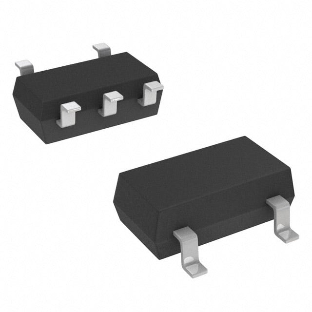
| 描述 | IC REG LDO 3.3V 50MA SOT323-5低压差稳压器 50mA Supply current Lo drop linear reg |
| 产品分类 | |
| 品牌 | STMicroelectronics |
| 产品手册 | |
| 产品图片 |
|
| rohs | 符合RoHS无铅 / 符合限制有害物质指令(RoHS)规范要求 |
| 产品系列 | 电源管理 IC,低压差稳压器,STMicroelectronics STLQ50C33R- |
| 数据手册 | |
| 产品型号 | STLQ50C33R |
| 产品培训模块 | http://www.digikey.cn/PTM/IndividualPTM.page?site=cn&lang=zhs&ptm=30339 |
| 产品目录页面 | |
| 产品种类 | Voltage Regulators |
| 供应商器件封装 | SOT-323-5 |
| 其它名称 | 497-5817-6 |
| 其它有关文件 | http://www.st.com/web/catalog/sense_power/FM142/CL1015/SC312/SS1731/PF181434?referrer=70071840 |
| 包装 | Digi-Reel® |
| 商标 | STMicroelectronics |
| 回动电压—最大值 | 700 mV at 50 mA |
| 安装类型 | 表面贴装 |
| 安装风格 | SMD/SMT |
| 封装 | Reel |
| 封装/外壳 | 6-TSSOP(5 引线),SC-88A,SOT-353 |
| 封装/箱体 | SOT-323 |
| 工作温度 | -40°C ~ 125°C |
| 工厂包装数量 | 3000 |
| 最大工作温度 | + 150 C |
| 最大输入电压 | 12 V |
| 最小工作温度 | - 40 C |
| 最小输入电压 | + 2.3 V |
| 标准包装 | 1 |
| 电压-跌落(典型值) | 0.4V @ 50mA |
| 电压-输入 | 最高 12V |
| 电压-输出 | 3.3V |
| 电压调节准确度 | 2 % |
| 电流-输出 | 50mA |
| 电流-限制(最小值) | - |
| 稳压器拓扑 | 正,固定式 |
| 稳压器数 | 1 |
| 系列 | STLQ50XX33 |
| 线路调整率 | 0.3 % |
| 负载调节 | 0.15 % |
| 输入偏压电流—最大 | 0.004 mA |
| 输出电压 | 3.3 V |
| 输出电流 | 50 mA |
| 输出端数量 | 1 Output |
| 输出类型 | Fixed |


- 商务部:美国ITC正式对集成电路等产品启动337调查
- 曝三星4nm工艺存在良率问题 高通将骁龙8 Gen1或转产台积电
- 太阳诱电将投资9.5亿元在常州建新厂生产MLCC 预计2023年完工
- 英特尔发布欧洲新工厂建设计划 深化IDM 2.0 战略
- 台积电先进制程称霸业界 有大客户加持明年业绩稳了
- 达到5530亿美元!SIA预计今年全球半导体销售额将创下新高
- 英特尔拟将自动驾驶子公司Mobileye上市 估值或超500亿美元
- 三星加码芯片和SET,合并消费电子和移动部门,撤换高东真等 CEO
- 三星电子宣布重大人事变动 还合并消费电子和移动部门
- 海关总署:前11个月进口集成电路产品价值2.52万亿元 增长14.8%


PDF Datasheet 数据手册内容提取
STLQ50 50 mA, 3 μA supply current low drop linear regulator Datasheet - production data The PMOS pass element allows very good dropout values (200 mV at 25 mA I and 350 mV O at full load) without affecting the consumption characteristics. Housed in the very small SOT323-5L, it meets space-saving requirements in battery-powered SOT323-5L equipment. Table 1. Device summary Features SOT323-5L (T&R) Output voltage • 2.3 V to 12 V input voltage range STLQ50C18R 1.8 V • 50 mA maximum output current STLQ50C25R 2.5 V • 3 µA quiescent current STLQ50C33R 3.3 V • Available in 1.8 V, 2.5 V, 3.3 V, 5.0 V and STLQ50C50R 5.0 V adjustable voltage STLQ50C-R Adjustable • 200 mV dropout voltage at 25 mA output current • Internal thermal protection • Available in SOT323-5L package Applications • Portable/battery-powered equipment • Electronic sensors • Microcontroller power • Real-time clock backup power Description The STLQ50 is a BiCMOS linear regulator specifically designed for operating in environments where very low power consumption is required. Its very low quiescent current (3 µA) results in extended battery life, making the device suitable for applications which have very long standby time. May 2014 DocID13205 Rev 6 1/18 This is information on a product in full production. www.st.com
Contents STLQ50 Contents 1 Block diagram . . . . . . . . . . . . . . . . . . . . . . . . . . . . . . . . . . . . . . . . . . . . . . 3 2 Pin configuration . . . . . . . . . . . . . . . . . . . . . . . . . . . . . . . . . . . . . . . . . . . . 4 3 Maximum ratings . . . . . . . . . . . . . . . . . . . . . . . . . . . . . . . . . . . . . . . . . . . . 5 4 Electrical characteristics . . . . . . . . . . . . . . . . . . . . . . . . . . . . . . . . . . . . . 6 5 Typical application . . . . . . . . . . . . . . . . . . . . . . . . . . . . . . . . . . . . . . . . . . 7 6 Typical characteristics . . . . . . . . . . . . . . . . . . . . . . . . . . . . . . . . . . . . . . . 8 7 Application information . . . . . . . . . . . . . . . . . . . . . . . . . . . . . . . . . . . . . 10 7.1 External components . . . . . . . . . . . . . . . . . . . . . . . . . . . . . . . . . . . . . . . . 10 7.2 Power dissipation . . . . . . . . . . . . . . . . . . . . . . . . . . . . . . . . . . . . . . . . . . . 10 7.3 Protection . . . . . . . . . . . . . . . . . . . . . . . . . . . . . . . . . . . . . . . . . . . . . . . . . .11 8 Package mechanical data . . . . . . . . . . . . . . . . . . . . . . . . . . . . . . . . . . . . 12 9 Packaging mechanical data . . . . . . . . . . . . . . . . . . . . . . . . . . . . . . . . . . 15 10 Revision history . . . . . . . . . . . . . . . . . . . . . . . . . . . . . . . . . . . . . . . . . . . 17 2/18 DocID13205 Rev 6
STLQ50 Block diagram 1 Block diagram Figure 1. Block diagram (fixed version) (cid:57) (cid:57) (cid:44)(cid:49) (cid:50)(cid:56)(cid:55) (cid:38)(cid:88)(cid:85)(cid:85)(cid:72)(cid:81)(cid:87)(cid:3) (cid:79)(cid:76)(cid:80)(cid:76)(cid:87) (cid:37)(cid:76)(cid:68)(cid:86)(cid:3) (cid:74)(cid:72)(cid:81)(cid:72)(cid:85)(cid:68)(cid:87)(cid:82)(cid:85) (cid:55)(cid:75)(cid:72)(cid:85)(cid:80)(cid:68)(cid:79) (cid:83)(cid:85)(cid:82)(cid:87)(cid:72)(cid:70)(cid:87)(cid:76)(cid:82)(cid:81) (cid:50)(cid:51)(cid:36)(cid:48)(cid:51) (cid:37)(cid:68)(cid:81)(cid:71)(cid:74)(cid:68)(cid:83) (cid:85)(cid:72)(cid:73)(cid:72)(cid:85)(cid:72)(cid:81)(cid:70)(cid:72) (cid:42)(cid:49)(cid:39) Figure 2. Block diagram (adjustable version) (cid:57) (cid:57) (cid:44)(cid:49) (cid:50)(cid:56)(cid:55) (cid:38)(cid:88)(cid:85)(cid:85)(cid:72)(cid:81)(cid:87)(cid:3) (cid:79)(cid:76)(cid:80)(cid:76)(cid:87) (cid:37)(cid:76)(cid:68)(cid:86)(cid:3) (cid:74)(cid:72)(cid:81)(cid:72)(cid:85)(cid:68)(cid:87)(cid:82)(cid:85) (cid:55)(cid:75)(cid:72)(cid:85)(cid:80)(cid:68)(cid:79) (cid:83)(cid:85)(cid:82)(cid:87)(cid:72)(cid:70)(cid:87)(cid:76)(cid:82)(cid:81) (cid:50)(cid:51)(cid:36)(cid:48)(cid:51) (cid:37)(cid:68)(cid:81)(cid:71)(cid:74)(cid:68)(cid:83) (cid:41)(cid:37) (cid:85)(cid:72)(cid:73)(cid:72)(cid:85)(cid:72)(cid:81)(cid:70)(cid:72) (cid:42)(cid:49)(cid:39) DocID13205 Rev 6 3/18 18
Pin configuration STLQ50 2 Pin configuration Figure 3. Pin connections (top view) (cid:36)(cid:39)(cid:45)(cid:18)(cid:49)(cid:38) (cid:20) (cid:24) (cid:50)(cid:56)(cid:55) (cid:42)(cid:49)(cid:39) (cid:21) (cid:49)(cid:18)(cid:38) (cid:22) (cid:23) (cid:44)(cid:49) Table 2. Pin description Pin n° Symbol Note ADJ ADJ pin on the Adjustable version 1 N/C Not connected on fixed version 2 GND Ground 3 N/C Not connected 4 IN Input voltage 5 OUT Output voltage 4/18 DocID13205 Rev 6
STLQ50 Maximum ratings 3 Maximum ratings Table 3. Absolute maximum ratings Symbol Parameter Value Unit V DC Input voltage -0.3 to +14 V I V ADJ pin voltage -0.3 to +7 V ADJ ESD Human body model ±2 kV T Junction temperature -40 to 150 °C J T Storage temperature range -55 to 150 °C STG Note: Absolute maximum ratings are those values beyond which damage to the device may occur. Functional operation under these conditions is not implied. Table 4. Thermal data Symbol Parameter SOT323-5L Unit R Thermal resistance junction-ambient 331.4 (1) °C/W thJA 1. This value is referred to a 4-layer PCB, JEDEC standard test board. DocID13205 Rev 6 5/18 18
Electrical characteristics STLQ50 4 Electrical characteristics V = V +1 V or V = 2.5 V if V < 1.5 V; T = -40 °C to 125 °C; I = 1 mA; typical values I O(NOM) I O A O are at T = 25 °C, C = 1 µF unless otherwise specified. A O Table 5. Electrical characteristics Symbol Parameter Test conditions Min. Typ. Max. Unit I = 20 mA 2.3 12 O V Input voltage range V I I = 50 mA 2.5 12 O Quiescent current (measured on VI = 5 V 3.5 5.0 I µA Q ground pin, fixed version) V = 12 V 4.1 6.0 I Output voltage range (STLQ50ADJ) 1.222 11 V VO Accuracy as percentage of nominal -2 +2 % voltage at T = 25 °C J V Max dropout voltage (1) I = 50 mA; 0.4 0.7 V DROP-MAX O ΔV Load regulation 1 mA < I < 50 mA 0.15 %/mA O O V = 1.5 V: O ΔV Line regulation VO + 1 V < VI < 12 V; 0.3 %/V O V < 1.5 V: O 2.5 V < V < 12 V; I V = 0.1 V, SVR Supply voltage rejection RIPPLE 30 dB I = 20 mA, f = 120 Hz O B from 200 Hz to eN Output noise voltage W 560 µV 100kHZ; I = 10 mA RMS O T Thermal protection 160 °C h I Maximum output current (2) V = 0 V 500 mA OMAX O 1. V = 2.5 V when V ≤ 2.1 V I O(NOM) 2. The maximum power dissipation must not be exceeded, see application information for details. 6/18 DocID13205 Rev 6
STLQ50 Typical application 5 Typical application Figure 4. Fixed versions Figure 5. Adjustable version DocID13205 Rev 6 7/18 18
Typical characteristics STLQ50 6 Typical characteristics Figure 6. V vs. T Figure 7. V vs. V O J O I 111...888444 22 111...888222 11..88 11..66 111...888 11..44 [V][V][V]OOO 111...777888 [V][V] 11..2211 VVV OO VV 00..88 111...777666 00..66 00..44 111...777444 VVVIII===222...888VVV,,, IIIOOO===222000mmmAAA 00..22 IIOO==5500mmAA,, VVOO==11..88VV 111...777222 00 ---555000 ---222555 000 222555 555000 777555 111000000 111222555 00 11 22 33 44 55 VV [[VV]] TTeemmpp [[°°CC]] II Figure 8. I vs. T Figure 9. V vs. I Q J DROP O 333...555 00..55 333...444 00..4455 00..44 333...333 00..3355 Iq[µA]Iq[µA]Iq[µA] 333333......222111 V[V]V[V]DROPDROP 000000..22....232355 333 00..1155 222...999 VVV===555VVV,,, III ===111mmmAAA,,, VVV ===111...888VVV 00..11 TTAA==2255°°CC III OOO OOO 00..0055 222...888 00 ---555000 ---222555 000 222555 555000 777555 111000000 111222555 00 1100 2200 3300 4400 5500 TTeemmpp [[°°CC]] II [[mmAA]] OO Figure 10. V vs. T Figure 11. Stability DROP J 1122 00..77 1111 TTAA==2255°°CC 00..66 1100 99 00..55 88 [V][V] 00..44 ΩΩ]] 77 OPOP R[R[ 66 VVDRDR 00..33 ESES 55 00..22 44 33 00..11 VV ==22..4455VV,, II ==5500mmAA 22 OO OO 00 11 --5500 --2255 00 2255 5500 7755 110000 112255 00 00 11 22 33 44 55 TTeemmpp [[°°CC]] CC [[µµFF]] OO 8/18 DocID13205 Rev 6
STLQ50 Typical characteristics Figure 12. S.V.R. vs. Freq. Figure 13. S.V.R. vs. I O 4400 3377 VV ==11..88VV,, II ==2200mmAA 3388 3322 OO OO 3366 3344 2277 B]B] B]B] 3322 R [dR [d 2222 R [dR [d 3300 VV 1177 VV 2288 SS SS 1122 2266 2244 77 2222 VVOO==11..88VV,, ff==112200HHzz 22 2200 110000 11000000 1100000000 110000000000 00 1100 2200 3300 4400 5500 FFrreeqquueennccyy [[HHzz]] II [[mmAA]] OO Figure 14. Line transient response Figure 15. Load transient response I =50mA; C =10µF; V=2.8V, V rise/fall=5ms C =1µF; V =1.8V; V=2.8V, Curr. rise/fall=1µs O O I I O O I Figure 16. Short-circuit current Figure 17. Thermal protection 000...666 22 VV==22..88VV 000...555 11..7755 II 11..55 000...444 11..2255 A]A]A] V]V] I[I[I[OOO 000...333 V[V[OO 11 00..7755 000...222 00..55 000...111 00..2255 VVVOOO===000,,, TTTAAA===222555°°°CCC 00 000 115555 115577 115599 116611 116633 116655 116677 116699 117711 117733 117755 222 444 666 888 111000 111222 111444 TT[[°°CC]] VV [[VV]] JJ II DocID13205 Rev 6 9/18 18
Application information STLQ50 7 Application information The STLQ50 is a BiCMOS linear regulator specifically designed for operating in environments with very low power consumption requirements. The very low quiescent current of 3 µA is obtained through the use of CMOS technology which makes the device suitable for application that have long standby time. Its very low power consumption allows extended battery life and the tiny packages (SOT323-5L) satisfy the space-saving requirements of battery-powered equipment. Moreover, the STLQ50 provides wide input voltage operation from 2.5 V up to 12 V. The PMOS pass element also permits a very good dropout values of 0.7 V at full load and at 125 °C without affecting consumption characteristics. 7.1 External components The typical application schematic of the STLQ50 is shown in Figure4 - Figure5, 1 µF input and output capacitors placed close to the device are required for proper operation. The device is stable with electrolytic and ceramic output capacitors having values higher than 1 µF (see Figure11 for stability details). In the adjustable version the output voltage is programmed using an external resistor divider, as shown in Figure5. The output voltage can be adjusted from 1.22 to 11 V and it can be calculated using the following equation: Equation 1 V = V x (1+R /R ) O FB 1 2 where V = 1.222 V is the internal reference voltage. FB The sum of the R and R resistors should be chosen in order to guarantee at least 1 µA of 1 2 divider current. Lower value resistors improve the noise performance but the quiescent current will increase. Higher value resistors should be avoided because the ADJ leakage current will influence the voltage set by the resistor divider, rendering the formula above no longer valid. The suggested design procedure is to choose R = 1 MΩ and then calculate R using the 2 1 following equation: Equation 2 R = (V /V -1) x R 1 O FB 2 7.2 Power dissipation In order to ensure proper operation, the STLQ50 junction temperature should never exceed 125 °C; this limits the maximum power dissipation the regulator can sustain in any application. The maximum power dissipation can be calculated as: Equation 3 P = (T - T )/R DMAX JMAX A thJA where T = 125 °C; JMAX 10/18 DocID13205 Rev 6
STLQ50 Application information T is the ambient temperature; A R is the junction-to-ambient thermal resistance of the package (seeTable4 thermal thJA data). The power dissipation can be calculated simply as: Equation 4 P = (V - V ) x I D I O O In every application condition, P must be lower than P . D DMAX 7.3 Protection The PMOS pass element has an internal diode with anode connected to V and cathode to O V. In case V > V, the current will flow from output to input without limitation. In this case, a I O I proper limiting network is recommended. The current limitation is automatically provided by the characteristics of the PMOS pass element (see typical characteristics), so the short-circuit current is dependent on the input voltage. When considering short-circuit current, take care in any case not to exceed the maximum sustainable power dissipation of the device. The STLQ50 features an internal thermal protection that linearly reduces the output current when the internal temperature increases. Consequently, at a given load, the output voltage decreases also. The action of the thermal protection starts at 125 °C when the output voltage slightly decreases, while close to 163 °C the output voltage drops to 0 V. Since this is a linear control, sudden overcurrent conditions can quickly raise the chip temperature without giving time for the thermal protection to act, so it cannot be used as a limitation for the output current. DocID13205 Rev 6 11/18 18
Package mechanical data STLQ50 8 Package mechanical data In order to meet environmental requirements, ST offers these devices in different grades of ECOPACK® packages, depending on their level of environmental compliance. ECOPACK specifications, grade definitions and product status are available at: www.st.com. ECOPACK is an ST trademark. 12/18 DocID13205 Rev 6
STLQ50 Package mechanical data Figure 18. SOT323-5L drawing (cid:26)(cid:19)(cid:28)(cid:20)(cid:23)(cid:20)(cid:22)(cid:66)(cid:73) DocID13205 Rev 6 13/18 18
Package mechanical data STLQ50 Table 6. SOT323-5L mechanical data mm Dim. Min. Typ. Max. A 0.80 1.10 A1 0 0.10 A2 0.80 0.90 1 b 0.15 0.30 c 0.10 0.22 D 1.80 2 2.20 E 1.80 2.10 2.40 E1 1.15 1.25 1.35 e 0.65 e1 1.30 L 0.26 0.36 0.46 < 0° 8° 14/18 DocID13205 Rev 6
STLQ50 Packaging mechanical data 9 Packaging mechanical data Figure 19. SOT323-xL tape and reel drawing DocID13205 Rev 6 15/18 18
Packaging mechanical data STLQ50 Table 7. SOT323-xL tape and reel mechanical data mm Dim. Min. Typ. Max. A 175 180 185 C 12.8 13 13.2 D 20.2 N 59.5 60 60.5 T 14.4 Ao 2.25 Bo 3.17 Ko 1.2 Po 3.9 4.0 4.1 P 3.9 4.0 4.2 16/18 DocID13205 Rev 6
STLQ50 Revision history 10 Revision history Table 8. Document revision history Date Revision Changes 07-Feb-2007 1 Initial release. 13-Feb-2007 2 Typo in cover page 350 mA ==> 350 mV. 06-Jul-2007 3 Added part number. 14-Nov-2007 4 Added Table1. – Modified line regulation test condition Table5 on page6. 31-Jan-2013 5 – Minor text changes throughout the document. Part number STLQ50xx changed to STLQ50. Removed SOT23-5L package. Updated Table1: Device summary, Section1: Block diagram, Section2: Pin configuration,Section3: Maximum ratings, Section5: 09-May-2014 6 Typical application, Section7: Application information, Section8: Package mechanical data. Added Section9: Packaging mechanical data. Minor text changes. DocID13205 Rev 6 17/18 18
STLQ50 Please Read Carefully: Information in this document is provided solely in connection with ST products. STMicroelectronics NV and its subsidiaries (“ST”) reserve the right to make changes, corrections, modifications or improvements, to this document, and the products and services described herein at any time, without notice. All ST products are sold pursuant to ST’s terms and conditions of sale. Purchasers are solely responsible for the choice, selection and use of the ST products and services described herein, and ST assumes no liability whatsoever relating to the choice, selection or use of the ST products and services described herein. No license, express or implied, by estoppel or otherwise, to any intellectual property rights is granted under this document. If any part of this document refers to any third party products or services it shall not be deemed a license grant by ST for the use of such third party products or services, or any intellectual property contained therein or considered as a warranty covering the use in any manner whatsoever of such third party products or services or any intellectual property contained therein. UNLESS OTHERWISE SET FORTH IN ST’S TERMS AND CONDITIONS OF SALE ST DISCLAIMS ANY EXPRESS OR IMPLIED WARRANTY WITH RESPECT TO THE USE AND/OR SALE OF ST PRODUCTS INCLUDING WITHOUT LIMITATION IMPLIED WARRANTIES OF MERCHANTABILITY, FITNESS FOR A PARTICULAR PURPOSE (AND THEIR EQUIVALENTS UNDER THE LAWS OF ANY JURISDICTION), OR INFRINGEMENT OF ANY PATENT, COPYRIGHT OR OTHER INTELLECTUAL PROPERTY RIGHT. ST PRODUCTS ARE NOT DESIGNED OR AUTHORIZED FOR USE IN: (A) SAFETY CRITICAL APPLICATIONS SUCH AS LIFE SUPPORTING, ACTIVE IMPLANTED DEVICES OR SYSTEMS WITH PRODUCT FUNCTIONAL SAFETY REQUIREMENTS; (B) AERONAUTIC APPLICATIONS; (C) AUTOMOTIVE APPLICATIONS OR ENVIRONMENTS, AND/OR (D) AEROSPACE APPLICATIONS OR ENVIRONMENTS. WHERE ST PRODUCTS ARE NOT DESIGNED FOR SUCH USE, THE PURCHASER SHALL USE PRODUCTS AT PURCHASER’S SOLE RISK, EVEN IF ST HAS BEEN INFORMED IN WRITING OF SUCH USAGE, UNLESS A PRODUCT IS EXPRESSLY DESIGNATED BY ST AS BEING INTENDED FOR “AUTOMOTIVE, AUTOMOTIVE SAFETY OR MEDICAL” INDUSTRY DOMAINS ACCORDING TO ST PRODUCT DESIGN SPECIFICATIONS. PRODUCTS FORMALLY ESCC, QML OR JAN QUALIFIED ARE DEEMED SUITABLE FOR USE IN AEROSPACE BY THE CORRESPONDING GOVERNMENTAL AGENCY. Resale of ST products with provisions different from the statements and/or technical features set forth in this document shall immediately void any warranty granted by ST for the ST product or service described herein and shall not create or extend in any manner whatsoever, any liability of ST. ST and the ST logo are trademarks or registered trademarks of ST in various countries. Information in this document supersedes and replaces all information previously supplied. The ST logo is a registered trademark of STMicroelectronics. All other names are the property of their respective owners. © 2014 STMicroelectronics - All rights reserved STMicroelectronics group of companies Australia - Belgium - Brazil - Canada - China - Czech Republic - Finland - France - Germany - Hong Kong - India - Israel - Italy - Japan - Malaysia - Malta - Morocco - Philippines - Singapore - Spain - Sweden - Switzerland - United Kingdom - United States of America www.st.com 18/18 DocID13205 Rev 6
Mouser Electronics Authorized Distributor Click to View Pricing, Inventory, Delivery & Lifecycle Information: S TMicroelectronics: STLQ50C18R STLQ50C25R STLQ50C-R STLQ50C33R STLQ50C50R