ICGOO在线商城 > 集成电路(IC) > 接口 - 驱动器,接收器,收发器 > ST1480ABDR
 Datasheet下载
- 型号: ST1480ABDR
- 制造商: STMicroelectronics
- 库位|库存: xxxx|xxxx
- 要求:
| 数量阶梯 | 香港交货 | 国内含税 |
| +xxxx | $xxxx | ¥xxxx |
查看当月历史价格
查看今年历史价格
ST1480ABDR产品简介:
ICGOO电子元器件商城为您提供ST1480ABDR由STMicroelectronics设计生产,在icgoo商城现货销售,并且可以通过原厂、代理商等渠道进行代购。 ST1480ABDR价格参考。STMicroelectronicsST1480ABDR封装/规格:接口 - 驱动器,接收器,收发器, 半 收发器 1/1 RS422,RS485 8-SO。您可以下载ST1480ABDR参考资料、Datasheet数据手册功能说明书,资料中有ST1480ABDR 详细功能的应用电路图电压和使用方法及教程。
STMicroelectronics的ST1480ABDR是一款接口驱动器、接收器和收发器,主要应用于高速数据传输和通信系统中。以下是其主要应用场景:

1. 工业自动化:ST1480ABDR适用于工业控制网络,如现场总线系统(Fieldbus),用于连接传感器、执行器和其他工业设备。它支持高可靠性和抗干扰性能,适合复杂的工业环境。

2. 汽车电子:在汽车领域,该器件可用于车载网络通信,例如CAN总线系统。它能够实现车辆内部各模块之间的高效数据交换,满足现代汽车对实时性和稳定性的要求。

3. 通信设备:适用于各种通信基础设施,如调制解调器、路由器和交换机等。通过提供稳定的信号驱动与接收功能,确保数据在网络中的准确传递。

4. 消费电子产品:可用于打印机、扫描仪及其他外围设备的数据接口设计,提升产品性能并增强用户体验。

5. 医疗仪器:在医疗监测设备或诊断工具中,ST1480ABDR可帮助实现精确的数据采集与处理,保障医疗信息的准确性。

总之,ST1480ABDR凭借其卓越的电气特性及可靠性,广泛应用于需要高效数据通信的各种场景。
| 参数 | 数值 |
| 产品目录 | 集成电路 (IC)半导体 |
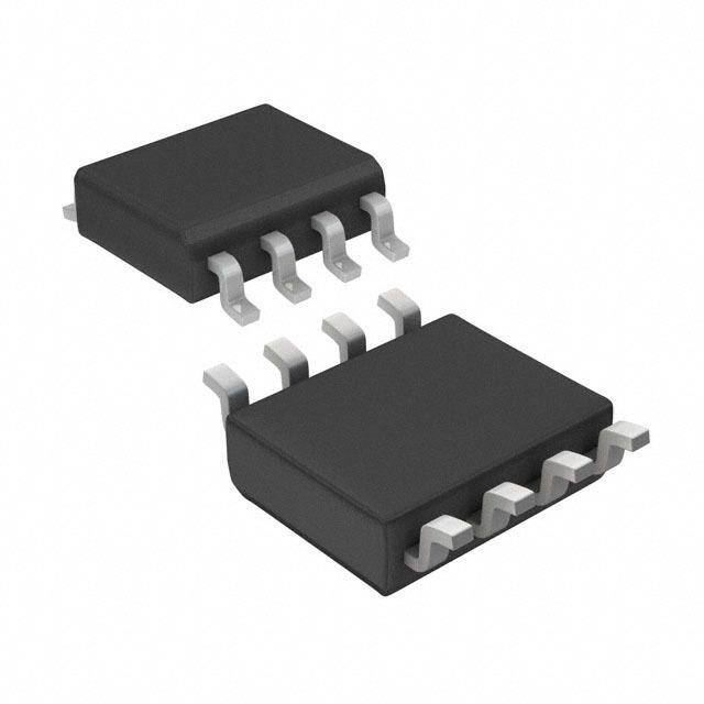
| 描述 | IC TXRX 3.3V RS485/422 8 SOIC缓冲器和线路驱动器 Trancvr Driver/Recvr |
| 产品分类 | |
| 品牌 | STMicroelectronics |
| 产品手册 | |
| 产品图片 |
|
| rohs | 符合RoHS无铅 / 符合限制有害物质指令(RoHS)规范要求 |
| 产品系列 | 逻辑集成电路,缓冲器和线路驱动器,STMicroelectronics ST1480ABDR- |
| 数据手册 | |
| 产品型号 | ST1480ABDR |
| 产品目录页面 | |
| 产品种类 | 缓冲器和线路驱动器 |
| 供应商器件封装 | 8-SO |
| 其它名称 | 497-2046-6 |
| 其它有关文件 | http://www.st.com/web/catalog/sense_power/FM1968/CL1179/SC393/PF66805?referrer=70071840 |
| 包装 | Digi-Reel® |
| 协议 | RS422,RS485 |
| 双工 | 半 |
| 商标 | STMicroelectronics |
| 安装类型 | 表面贴装 |
| 安装风格 | SMD/SMT |
| 封装 | Reel |
| 封装/外壳 | 8-SOIC(0.154",3.90mm 宽) |
| 封装/箱体 | SO-8 |
| 工作温度 | -40°C ~ 85°C |
| 工厂包装数量 | 2500 |
| 接口 | RS-422. RS-485 |
| 接收器滞后 | 30µV |
| 数据速率 | 15 Mbps |
| 最大工作温度 | + 85 C |
| 最小工作温度 | - 40 C |
| 标准包装 | 1 |
| 电压-电源 | 3 V ~ 3.6 V |
| 电源电压-最大 | 3.6 V |
| 电源电压-最小 | 3 V |
| 电源电流 | 2.2 mA |
| 类型 | 收发器 |
| 系列 | ST1480 |
| 驱动器/接收器数 | 1/1 |


- 商务部:美国ITC正式对集成电路等产品启动337调查
- 曝三星4nm工艺存在良率问题 高通将骁龙8 Gen1或转产台积电
- 太阳诱电将投资9.5亿元在常州建新厂生产MLCC 预计2023年完工
- 英特尔发布欧洲新工厂建设计划 深化IDM 2.0 战略
- 台积电先进制程称霸业界 有大客户加持明年业绩稳了
- 达到5530亿美元!SIA预计今年全球半导体销售额将创下新高
- 英特尔拟将自动驾驶子公司Mobileye上市 估值或超500亿美元
- 三星加码芯片和SET,合并消费电子和移动部门,撤换高东真等 CEO
- 三星电子宣布重大人事变动 还合并消费电子和移动部门
- 海关总署:前11个月进口集成电路产品价值2.52万亿元 增长14.8%


PDF Datasheet 数据手册内容提取
ST1480AB ST1480AC 3.3 V powered, 15 kV ESD protected, up to 12 Mbps true RS-485/RS-422 transceiver Datasheet - production data Description The ST1480Ax is ±15kV ESD protected, 3.3V low power transceiver for RS-485 and RS-422 communications. The device contains one driver and one receiver in half duplex configuration. The ST1480Ax transmits and receives at a guaranteed data rate of at least 12Mbps. DIP-8 SO-8 All transmitter outputs and receiver inputs are protected to ±15 kV using Human Body Model. Driver is short-circuit current limited and is protected against excessive power dissipation by Features thermal shutdown circuitry that places the driver • ESD protection outputs into a high-impedance state. – ±15 kV human body model The ST1480Ax input has a true fail-safe feature – ±8 kV IEC 1000-4-2 contact discharge that guarantees a logic high output if both inputs are open circuit, shorted together or in the • Operates from a single 3.3 V supply - no presence of a termination with no signal on the charge pump required bus. • Interoperable with 5V logic • 1µA low current shutdown mode max • Guaranteed 12Mbps data rate • -7 to 12 common mode input voltage range • Half duplex versions available • Industry standard 75176 pinout • Current limiting and thermal shutdown for driver overload protection • Guaranteed high receiver output state for floating, shorted or terminated inputs with no signal present • Allows up to 64 transceivers on the bus Table 1. Device summary Order codes Temperature range Package Packaging ST1480ACN 0 to 70 °C DIP-8 50 parts per tube / 40 tube per box ST1480ACDR 0 to 70 °C SO-8 (tape & reel) 2500 parts per reel ST1480ABDR -40 to 85 °C SO-8 (tape & reel) 2500 parts per reel July 2013 DocID9101 Rev 4 1/21 This is information on a product in full production. www.st.com
Contents ST1480AB - ST1480AC Contents 1 Pin configuration . . . . . . . . . . . . . . . . . . . . . . . . . . . . . . . . . . . . . . . . . . . . 3 2 Truth tables . . . . . . . . . . . . . . . . . . . . . . . . . . . . . . . . . . . . . . . . . . . . . . . . 4 3 Maximum ratings . . . . . . . . . . . . . . . . . . . . . . . . . . . . . . . . . . . . . . . . . . . . 5 4 Electrical characteristics . . . . . . . . . . . . . . . . . . . . . . . . . . . . . . . . . . . . . 6 5 Test circuits and typical characteristics . . . . . . . . . . . . . . . . . . . . . . . . . 9 6 Package mechanical data . . . . . . . . . . . . . . . . . . . . . . . . . . . . . . . . . . . . 17 7 Revision history . . . . . . . . . . . . . . . . . . . . . . . . . . . . . . . . . . . . . . . . . . . 20 2/21 DocID9101 Rev 4
ST1480AB - ST1480AC Pin configuration 1 Pin configuration Figure 1. Pin connections Figure 2. Pin description Pin n° Symbol Name and function 1 RO Receiver output. If A>B by 200mV, RO is high; if A<B by 200mV, RO is low Receiver Output Enable. RO is enabled when RE is low; RO is high impedance when RE 2 RE is high. If RE is high and DE is low, the device enters a low power shutdown mode. Driver Output Enable. The driver outputs are enabled by bringing DE high. They are high impedance when DE is low. If RE is high DE is low, the device enters a low-power 3 DE shutdown mode. If the driver outputs are enabled, the part functions as line driver, while they are high impedance, it functions as line receivers if RE is low. Driver input. A low on DI forces output A low and output B high. Similarly, a high on DI 4 DI forces output A high and output B low 5 GND Ground 6 A Non-inverting receiver input and non-inverting driver output 7 B Inverting receiver input and inverting driver output 8 V Supply voltage: V = 3V to 3.6V CC CC DocID9101 Rev 4 3/21 21
Truth tables ST1480AB - ST1480AC 2 Truth tables Table 2. Truth table (driver) Inputs Outputs Mode RE DE DI B A X H H L H Normal X H L H L Normal L L X Z Z Normal H L X Z Z Shutdown Note: X= Don’t care; Z=High impedance Table 3. Truth table (receiver) Inputs Output Mode RE DE A-B RO L L ≥ -0.015V H Normal L L ≤ -0.2V L Normal L L Inputs open H Normal L L Inputs shorted H Normal H L X Z Shutdown Note: X= Don’t care; Z=High impedance 4/21 DocID9101 Rev 4
ST1480AB - ST1480AC Maximum ratings 3 Maximum ratings Table 4. Absolute maximum ratings Symbol Parameter Value Unit V Supply voltage 7 V CC V Control input voltage (RE, DE) -0.3 to 7 V I V Driver input voltage (DI) -0.3 to 7 V DI V Driver output voltage (A, B) ± 14 V DO V Receiver input voltage (A, B) ± 14 V RI V Receiver output voltage (RO) -0.3 to (V + 0.3) V RO CC Note: Absolute maximum ratings are those values beyond which damage to the device may occur. Functional operation under these condition is not implied. Table 5. ESD performance: transmitter outputs, receiver inputs Symbol Parameter Test conditions Min. Typ. Max. Unit ESD ESD protection voltage Human body model ± 15 kV ESD ESD protection voltage IEC-1000-4-2 contact discharge ± 8 kV DocID9101 Rev 4 5/21 21
Electrical characteristics ST1480AB - ST1480AC 4 Electrical characteristics V = 3 V to 3.6 V, TA = -40 to 85 °C, unless otherwise specified. Typical values are referred CC to TA = 25 °C). Table 6. Electrical characteristics Symbol Parameter Test conditions Min. Typ. Max. Unit DE=V , CC RE=0V or 1.3 2.2 mA ISUPPLY VCC Power supply current NVo Load, DI=0V or VCC CC DE=0V, 1.2 1.9 mA RE=0V I Shutdown supply current DE=0V, RE=V , DI=0V or V 0.002 1 µA SHDN CC CC Table 7. Logic input electrical characteristics Symbol Parameter Test conditions Min. Typ. Max. Unit V Input logic threshold low DE, DI, RE 1.3 0.8 V IL V Input logic threshold high DE, DI, RE 2 V IH I Logic input current DE, DI, RE ± 2.0 µA IN1 V =12V 1 mA IN I Input current (A, B) DE=0V, V = 0 or 3.6V IN2 CC V =-7V -0.8 mA IN Table 8. Transmitter electrical characteristics Symbol Parameter Test conditions Min. Typ. Max. Unit R = 100Ω (RS-422) (Figure1) 2 V L V Differential drive output R = 54Ω (RS-485) (Figure1) 1.5 V OD L R = 60Ω (RS-485) (Figure3) 1.5 V L Change in magnitude of driver differential output voltage for ΔV R = 54Ω or 100Ω (Figure1) 0.2 V OD complementary output states L (Note: 1) Driver common mode output V R = 54Ω or 100Ω (Figure1) 3 V OC voltage L Change in magnitude of driver ΔV common mode output voltage R = 54Ω or 100Ω (Figure1) 0.2 V OC L (Note: 1) Driver short circuit output I ± 250 mA OSD current 6/21 DocID9101 Rev 4
ST1480AB - ST1480AC Electrical characteristics Table 9. Receiver electrical characteristics Symbol Parameter Test Conditions Min. Typ. Max. Unit Receiver differential V V = -7V to 12V, DE = 0 -0.2 -0.015 V TH threshold voltage CM ΔV Receiver input hysteresis V = 0V 30 µV TH CM Receiver output high V I = -4mA, V = 200mV, (Figure9) 2 V OH voltage OUT ID Receiver output low V I = 4mA, V = -200mV, (Figure4) 0.4 V OL voltage OUT ID 3-state (high impedance) I V = 3.6V, V = 0V to V ± 1 µA OZR output current at receiver CC O CC R Receiver input resistance V = -7V to 12V 24 kΩ RIN CM Receiver short-circuit I V = 0V to V 7 60 mA OSR current RO CC Table 10. Driver switching characteristics Symbol Parameter Test Conditions Min. Typ. Max. Unit D Maximum data rate 12 15 Mbps R R = 60Ω, C = 15pF, (Figure5 and t Differential output delay L L 18 30 ns DD Figure6) Differential output R = 60Ω, C = 15pF, (Figure5 and t L L 12 20 ns TD transition time Figure6) t R = 27Ω, C = 15pF, (Figure9 and PLH Propagation delay L L 18 30 ns t Figure10) PHL |t t | propagation R = 27Ω, C = 15pF, (Figure9 and t PLH - PHL L L 2 5 ns PDS delay skew (Note2) Figure10) t Output enable time R = 110Ω, (Figure11 and Figure12) 19 35 ns PZL L t Output enable time R = 110Ω, (Figure7 and Figure8) 30 50 ns PZH L t Output disable time R = 110Ω, (Figure7 and Figure8) 19 35 ns PHZ L t Output disable time R = 110Ω, (Figure11 and Figure12) 30 50 ns PLZ L Differential output delay t 1 3 ns SKEW skew Driver enable from t 30 50 ns ZH(SHDN) shutdown to output high Driver enable from t 19 35 ns ZL(SHDN) shutdown to output low DocID9101 Rev 4 7/21 21
Electrical characteristics ST1480AB - ST1480AC Table 11. Receiver switching characteristics Symbol Parameter Test Conditions Min. Typ. Max. Unit t V = 0V to 3V, C =15pF PLH Propagation delay ID L1 30 50 ns t (Figure13 and Figure14) PHL |t t | propagation V = 0V to 3V, C = 15pF t PLH - PHL ID L1 1 3 ns RPDS delay skew (Figure13 and Figure14) t Output enable time C = 15pF, (Figure15 and Figure19) 10 20 ns PZL RL t Output enable time C = 15pF, (Figure15 and Figure19) 10 20 ns PZH RL t Output disable time C = 15pF, (Figure15 and Figure19) 10 20 ns PHZ RL t Output disable time C = 15pF, (Figure15 and Figure19) 10 20 ns PLZ RL Receiver enable from t C = 15pF, (Figure15 and Figure19) 10 20 ns ZH(SHDN) shutdown to output high RL Receiver enable from t C = 15pF, (Figure15 and Figure19) 20 40 µs ZL(SHDN) shutdown to output low RL Note: 1 ΔV and ΔV are the changes in V and V , respectively, when the DI input changes OD OC OD OC state. 2 Measured on |t (A)-t (A)| and |t (B)-t (B)| PLH PHL PLH PHL 3 The transceivers are put into shutdown by bring RE high and DE low. If the input are in state for less than 80ns, the part are guaranteed not to enter shutdown. If the inputs are in this state for at least 300ns, the parts are guaranteed to have entered shutdown. 8/21 DocID9101 Rev 4
ST1480AB - ST1480AC Test circuits and typical characteristics 5 Test circuits and typical characteristics Figure 3. Driver and V test load OC Figure 4. Driver V with varying common mode voltage test load OD Figure 5. Receiver V and V test circuit OH OL DocID9101 Rev 4 9/21 21
Test circuits and typical characteristics ST1480AB - ST1480AC Figure 6. Drive differential output delay transition time test circuit Figure 7. Drive differential output delay transition time waveform Figure 8. Drive enable and disable times test circuit 10/21 DocID9101 Rev 4
ST1480AB - ST1480AC Test circuits and typical characteristics Figure 9. Drive enable and disable times waveforms Figure 10. Drive propagation time test circuit Figure 11. Drive propagation time waveform DocID9101 Rev 4 11/21 21
Test circuits and typical characteristics ST1480AB - ST1480AC Figure 12. Drive enable and disable times test circuit Figure 13. Drive enable and disable times waveforms Figure 14. Receiver propagation delay time test circuit 12/21 DocID9101 Rev 4
ST1480AB - ST1480AC Test circuits and typical characteristics Figure 15. Receiver propagation delay time waveforms Figure 16. Receiver enable and disable times test circuit Figure 17. Receiver enable and disable times waveform DocID9101 Rev 4 13/21 21
Test circuits and typical characteristics ST1480AB - ST1480AC Figure 18. Receiver enable and disable times waveform Figure 19. Receiver enable and disable times waveform Figure 20. Receiver enable and disable times waveform 14/21 DocID9101 Rev 4
ST1480AB - ST1480AC Test circuits and typical characteristics Figure 21. Receiver output current vs output Figure 22. Receiver output current vs output low voltage high voltage Figure 23. Low level driver output capability Figure 24. High level driver output capability Figure 25. Receiver input characteristics Figure 26. Driver short circuit current DocID9101 Rev 4 15/21 21
Test circuits and typical characteristics ST1480AB - ST1480AC Figure 27. Driver short circuit current 16/21 DocID9101 Rev 4
ST1480AB - ST1480AC Package mechanical data 6 Package mechanical data In order to meet environmental requirements, ST offers these devices in different grades of ECOPACK® packages, depending on their level of environmental compliance. ECOPACK® specifications, grade definitions and product status are available at: www.st.com. ECOPACK® is an ST trademark. Plastic DIP-8 mechanical data mm. inch. Dim. Min. Typ. Max. Min. Typ. Max. A 3.3 0.130 a1 0.7 0.028 B 1.39 1.65 0.055 0.065 B1 0.91 1.04 0.036 0.041 b 0.5 0.020 b1 0.38 0.5 0.015 0.020 D 9.8 0.386 E 8.8 0.346 e 2.54 0.100 e3 7.62 0.300 e4 7.62 0.300 F 7.1 0.280 I 4.8 0.189 L 3.3 0.130 Z 0.44 1.6 0.017 0.063 P001F DocID9101 Rev 4 17/21 21
Package mechanical data ST1480AB - ST1480AC SO-8 mechanical data mm. inch. Dim. Min. Typ. Max. Min. Typ. Max. A 1.35 1.75 0.053 0.069 A1 0.10 0.25 0.04 0.010 A2 1.10 1.65 0.043 0.065 B 0.33 0.51 0.013 0.020 C 0.19 0.25 0.007 0.010 D 4.80 5.00 0.189 0.197 E 3.80 4.00 0.150 0.157 e 1.27 0.050 H 5.80 6.20 0.228 0.244 h 0.25 0.50 0.010 0.020 L 0.40 1.27 0.016 0.050 k 8° (max.) ddd 0.1 0.04 0016023/C 18/21 DocID9101 Rev 4
ST1480AB - ST1480AC Package mechanical data Tape & reel SO-8 mechanical data mm. inch. Dim. Min. Typ. Max. Min. Typ. Max. A 330 12.992 C 12.8 13.2 0.504 0.519 D 20.2 0.795 N 60 2.362 T 22.4 0.882 Ao 8.1 8.5 0.319 0.335 Bo 5.5 5.9 0.216 0.232 Ko 2.1 2.3 0.082 0.090 Po 3.9 4.1 0.153 0.161 P 7.9 8.1 0.311 0.319 DocID9101 Rev 4 19/21 21
Revision history ST1480AB - ST1480AC 7 Revision history Table 12. Document revision history Date Revision Changes 02-May-2006 2 Order codes updated. 19-Nov-2007 3 Added Table2. Updated: ECOPACK® section in Chapter6 . 24-Jul-2013 4 Corrected: unit of measurement in Table9 (Receiver input hysteresis from V to µV).Minor text changes. 20/21 DocID9101 Rev 4
ST1480AB - ST1480AC Please Read Carefully: Information in this document is provided solely in connection with ST products. STMicroelectronics NV and its subsidiaries (“ST”) reserve the right to make changes, corrections, modifications or improvements, to this document, and the products and services described herein at any time, without notice. All ST products are sold pursuant to ST’s terms and conditions of sale. Purchasers are solely responsible for the choice, selection and use of the ST products and services described herein, and ST assumes no liability whatsoever relating to the choice, selection or use of the ST products and services described herein. No license, express or implied, by estoppel or otherwise, to any intellectual property rights is granted under this document. If any part of this document refers to any third party products or services it shall not be deemed a license grant by ST for the use of such third party products or services, or any intellectual property contained therein or considered as a warranty covering the use in any manner whatsoever of such third party products or services or any intellectual property contained therein. UNLESS OTHERWISE SET FORTH IN ST’S TERMS AND CONDITIONS OF SALE ST DISCLAIMS ANY EXPRESS OR IMPLIED WARRANTY WITH RESPECT TO THE USE AND/OR SALE OF ST PRODUCTS INCLUDING WITHOUT LIMITATION IMPLIED WARRANTIES OF MERCHANTABILITY, FITNESS FOR A PARTICULAR PURPOSE (AND THEIR EQUIVALENTS UNDER THE LAWS OF ANY JURISDICTION), OR INFRINGEMENT OF ANY PATENT, COPYRIGHT OR OTHER INTELLECTUAL PROPERTY RIGHT. ST PRODUCTS ARE NOT AUTHORIZED FOR USE IN WEAPONS. NOR ARE ST PRODUCTS DESIGNED OR AUTHORIZED FOR USE IN: (A) SAFETY CRITICAL APPLICATIONS SUCH AS LIFE SUPPORTING, ACTIVE IMPLANTED DEVICES OR SYSTEMS WITH PRODUCT FUNCTIONAL SAFETY REQUIREMENTS; (B) AERONAUTIC APPLICATIONS; (C) AUTOMOTIVE APPLICATIONS OR ENVIRONMENTS, AND/OR (D) AEROSPACE APPLICATIONS OR ENVIRONMENTS. WHERE ST PRODUCTS ARE NOT DESIGNED FOR SUCH USE, THE PURCHASER SHALL USE PRODUCTS AT PURCHASER’S SOLE RISK, EVEN IF ST HAS BEEN INFORMED IN WRITING OF SUCH USAGE, UNLESS A PRODUCT IS EXPRESSLY DESIGNATED BY ST AS BEING INTENDED FOR “AUTOMOTIVE, AUTOMOTIVE SAFETY OR MEDICAL” INDUSTRY DOMAINS ACCORDING TO ST PRODUCT DESIGN SPECIFICATIONS. PRODUCTS FORMALLY ESCC, QML OR JAN QUALIFIED ARE DEEMED SUITABLE FOR USE IN AEROSPACE BY THE CORRESPONDING GOVERNMENTAL AGENCY. Resale of ST products with provisions different from the statements and/or technical features set forth in this document shall immediately void any warranty granted by ST for the ST product or service described herein and shall not create or extend in any manner whatsoever, any liability of ST. ST and the ST logo are trademarks or registered trademarks of ST in various countries. Information in this document supersedes and replaces all information previously supplied. The ST logo is a registered trademark of STMicroelectronics. All other names are the property of their respective owners. © 2013 STMicroelectronics - All rights reserved STMicroelectronics group of companies Australia - Belgium - Brazil - Canada - China - Czech Republic - Finland - France - Germany - Hong Kong - India - Israel - Italy - Japan - Malaysia - Malta - Morocco - Philippines - Singapore - Spain - Sweden - Switzerland - United Kingdom - United States of America www.st.com DocID9101 Rev 4 21/21 21
Mouser Electronics Authorized Distributor Click to View Pricing, Inventory, Delivery & Lifecycle Information: S TMicroelectronics: ST1480ACDR ST1480ABDR ST1480ABN ST1480ACN