
 Datasheet下载
- 型号: SST39VF801C-70-4I-B3KE
- 制造商: Microchip
- 库位|库存: xxxx|xxxx
- 要求:
| 数量阶梯 | 香港交货 | 国内含税 |
| +xxxx | $xxxx | ¥xxxx |
查看当月历史价格
查看今年历史价格
SST39VF801C-70-4I-B3KE产品简介:
ICGOO电子元器件商城为您提供SST39VF801C-70-4I-B3KE由Microchip设计生产,在icgoo商城现货销售,并且可以通过原厂、代理商等渠道进行代购。 SST39VF801C-70-4I-B3KE价格参考。MicrochipSST39VF801C-70-4I-B3KE封装/规格:存储器, FLASH 存储器 IC 8Mb (512K x 16) 并联 70ns 48-TFBGA(6x8)。您可以下载SST39VF801C-70-4I-B3KE参考资料、Datasheet数据手册功能说明书,资料中有SST39VF801C-70-4I-B3KE 详细功能的应用电路图电压和使用方法及教程。
SST39VF801C-70-4I-B3KE 是由 Microchip Technology 生产的一款闪存存储器,属于并行 NOR Flash 类型。以下是其主要应用场景:

 1. 嵌入式系统
   - 该型号的闪存常用于嵌入式系统的代码存储和数据存储。例如,在工业控制、医疗设备或家用电器中,可以用来存储固件程序和配置参数。
   - 其高速读取性能(70ns)使其适合需要快速启动的应用场景。

 2. 消费电子
   - 在消费电子产品中,如打印机、扫描仪、数码相机等,SST39VF801C 可以用作引导存储器,存储启动所需的 BIOS 或固件。
   - 它的高可靠性确保了设备在长时间运行中的稳定性。

 3. 工业自动化
   - 工业自动化领域需要可靠的存储解决方案,SST39VF801C 的宽工作温度范围(-40°C 至 +85°C)和高耐用性使其成为理想选择。
   - 适用于 PLC(可编程逻辑控制器)、HMI(人机界面)和数据记录设备等。

 4. 汽车电子
   - 在汽车行业中,该型号可用于仪表盘、导航系统和发动机控制单元(ECU)中,提供稳定的数据存储功能。
   - 其非易失性特性确保断电后数据不会丢失。

 5. 通信设备
   - 在路由器、交换机和其他网络设备中,SST39VF801C 可以作为引导存储器,存储启动代码和配置信息。
   - 高速访问时间支持实时数据处理需求。

 6. 安全与监控
   - 在安防摄像头、门禁系统和报警系统中,该芯片可用于存储关键算法、日志文件或配置信息。
   - 其高可靠性和低功耗特性非常适合电池供电的设备。

 7. 物联网(IoT)
   - 在 IoT 设备中,SST39VF801C 可以存储固件和传感器数据,支持远程升级和本地数据记录。
   - 其小封装和低功耗设计非常适合紧凑型 IoT 应用。

总结来说,SST39VF801C-70-4I-B3KE 凭借其高性能、高可靠性和广泛的工作温度范围,适用于多种嵌入式、工业和消费类应用,尤其是在需要快速启动和非易失性存储的场景中表现优异。
| 参数 | 数值 |
| 产品目录 | 集成电路 (IC)半导体 |
| 描述 | IC FLASH 8MBIT 70NS 48TFBGA闪存 2.7 to 3.6V 8Mbit Multi-Purpose 闪存 |
| 产品分类 | |
| 品牌 | Microchip Technology |
| 产品手册 | |
| 产品图片 |
|
| rohs | 符合RoHS无铅 / 符合限制有害物质指令(RoHS)规范要求 |
| 产品系列 | 内存,闪存,Microchip Technology SST39VF801C-70-4I-B3KESST39 MPF™ |
| 数据手册 | http://www.microchip.com/mymicrochip/filehandler.aspx?ddocname=en555894http://www.microchip.com/mymicrochip/filehandler.aspx?ddocname=en556157 |
| 产品型号 | SST39VF801C-70-4I-B3KE |
| 产品种类 | 闪存 |
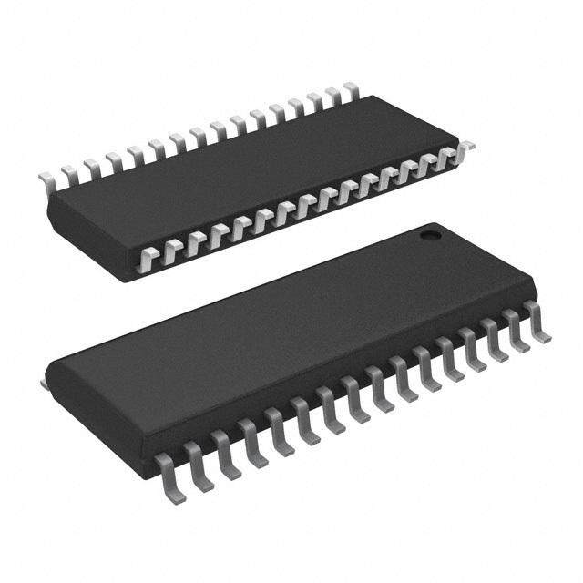
| 供应商器件封装 | 48-TFBGA(6x8) |
| 其它名称 | SST39VF801C704IB3KE |
| 包装 | 托盘 |
| 商标 | Microchip Technology |
| 存储器类型 | FLASH |
| 存储容量 | 8 Mbit |
| 存储类型 | NOR |
| 安装风格 | SMD/SMT |
| 定时类型 | Asynchronous |
| 封装 | Tray |
| 封装/外壳 | 48-TFBGA |
| 封装/箱体 | TFBGA-48 |
| 工作温度 | - 40 C to + 85 C |
| 工作温度范围 | - 40 C to + 85 C |
| 工厂包装数量 | 480 |
| 接口 | 并联 |
| 接口类型 | Parallel |
| 数据总线宽度 | 16 bit |
| 最大工作电流 | 18 mA |
| 标准包装 | 480 |
| 格式-存储器 | 闪存 |
| 电压-电源 | 2.7 V ~ 3.6 V |
| 电源电压-最大 | 3.6 V |
| 电源电压-最小 | 2.7 V |
| 系列 | SST39VF |
| 组织 | 512 k x 16 |
| 结构 | Sector |
| 访问时间 | 70 ns |
| 速度 | 70 ns |


_renders/MR4A16BCYS35.jpg)


- 商务部:美国ITC正式对集成电路等产品启动337调查
- 曝三星4nm工艺存在良率问题 高通将骁龙8 Gen1或转产台积电
- 太阳诱电将投资9.5亿元在常州建新厂生产MLCC 预计2023年完工
- 英特尔发布欧洲新工厂建设计划 深化IDM 2.0 战略
- 台积电先进制程称霸业界 有大客户加持明年业绩稳了
- 达到5530亿美元!SIA预计今年全球半导体销售额将创下新高
- 英特尔拟将自动驾驶子公司Mobileye上市 估值或超500亿美元
- 三星加码芯片和SET,合并消费电子和移动部门,撤换高东真等 CEO
- 三星电子宣布重大人事变动 还合并消费电子和移动部门
- 海关总署:前11个月进口集成电路产品价值2.52万亿元 增长14.8%
_renders/IS41C16100C-50KLI.jpg)


_renders/IS45S16320F-7BLA1.jpg)


PDF Datasheet 数据手册内容提取
8 Mbit (x16) Multi-Purpose Flash Plus SST39VF801C/SST39VF802C/SST39LF801C/SST39LF802C A Microchip Technology Company DataSheet The SST39VF801C / SST39VF802C / SST39LF801C / SST39LF802C are 512K x16 CMOS Multi-Purpose Flash Plus (MPF+) manufactured with SST proprietary, high performance CMOS SuperFlash® technology. The split-gate cell design and thick-oxide tunneling injector attain better reliability and manufacturability com- pared with alternate approaches. The SST39VF801C / SST39VF802C / SST39LF801C / SST39LF802C write (Program or Erase) with a 2.7-3.6V power supply. These devices conforms to JEDEC standard pinouts for x16 memories. Features (cid:129) Organizedas512Kx16 (cid:129) Security-IDFeature –SST:128bits;User:128words (cid:129) SingleVoltageReadandWriteOperations –2.7-3.6VforSST39VF801C/802C (cid:129) FastReadAccessTime: –3.0-3.6VforSST39LF801C/802C –70nsforSST39VF801C/802C –55nsforSST39LF801C/802C (cid:129) SuperiorReliability –Endurance:100,000Cycles(Typical) (cid:129) FastEraseandWord-Program: –Greaterthan100yearsDataRetention –Sector-EraseTime:18ms(typical) –Block-EraseTime:18ms(typical) (cid:129) LowPowerConsumption(typicalvaluesat5MHz) –Chip-EraseTime:40ms(typical) –ActiveCurrent:5mA(typical) –Word-ProgramTime:7µs(typical) –StandbyCurrent:3µA(typical) –AutoLowPowerMode:3µA(typical) (cid:129) AutomaticWriteTiming –InternalV Generation (cid:129) HardwareBlock-Protection/WP#InputPin PP –TopBlock-Protection(top8KWord) (cid:129) End-of-WriteDetection –BottomBlock-Protection(bottom8KWord) –ToggleBits –Data#Polling (cid:129) Sector-EraseCapability –Ready/Busy#Pin –Uniform2KWordsectors (cid:129) CMOSI/OCompatibility (cid:129) Block-EraseCapability (cid:129) JEDECStandard –Flexibleblockarchitecture;one8-,two4-,one16-,and fifteen32-KWordblocks –FlashEEPROMPinoutsandcommandsets (cid:129) Chip-EraseCapability (cid:129) PackagesAvailable –48-leadTSOP(12mmx20mm) (cid:129) Erase-Suspend/Erase-ResumeCapabilities –48-ballTFBGA(6mmx8mm) –48-ballWFBGA(4mmx6mm) (cid:129) HardwareResetPin(RST#) (cid:129) AlldevicesareRoHScompliant (cid:129) LatchedAddressandData www.microchip.com ©2011SiliconStorageTechnology,Inc. DS25041A 05/11
8 Mbit (x16) Multi-Purpose Flash Plus SST39VF801C/SST39VF802C/SST39LF801C/SST39LF802C A Microchip Technology Company DataSheet Product Description The SST39VF801C/802C and SST39LF801C/802C devices are 512K x16 CMOS Multi-Purpose Flash Plus (MPF+) manufactured with SST proprietary, high performance CMOS SuperFlash technology. Thesplit-gatecelldesignandthick-oxidetunnelinginjectorattainbetterreliabilityandmanufacturability comparedwithalternateapproaches.TheSST39VF801C/802CandSST39LF801C/802Cwrite(Program or Erase) with a 2.7-3.6V power supply. These devices conform to JEDEC standard pinouts for x16 memories. Featuring high performance Word-Program, the SST39VF801C/802C and SST39LF801C/802C devicesprovideatypicalWord-Programtimeof7µsec.ThesedevicesuseToggleBit,Data#Polling, or the RY/BY# pin to indicate the completion of Program operation. To protect against inadvertent write, they have on-chip hardware and Software Data Protection schemes. Designed, manufactured, and tested for a wide spectrum of applications, these devices are offered with a guaranteed typical enduranceof100,000cycles.Dataretentionisratedatgreaterthan100years. The SST39VF801C/802C and SST39LF801C/802C devices are suited for applications that require convenient and economical updating of program, configuration, or data memory. For all system appli- cations,theysignificantlyimproveperformanceandreliability,whileloweringpowerconsumption.They inherently use less energy during Erase and Program than alternative flash technologies. The total energy consumed is a function of the applied voltage, current, and time of application. Since for any givenvoltagerange,theSuperFlashtechnologyuseslesscurrenttoprogramandhasashortererase time, the total energy consumed during any Erase or Program operation is less than alternative flash technologies.Thesedevicesalsoimproveflexibilitywhileloweringthecostforprogram,data,andcon- figurationstorageapplications. The SuperFlash technology provides fixed Erase and Program times, independent of the number of Erase/Program cycles that have occurred. Therefore the system software or hardware does not have to be modified or de-rated as is necessary with alternative flash technologies, whose Erase and Pro- gramtimesincreasewithaccumulatedErase/Programcycles. To meet high density, surface mount requirements, the SST39VF801C/802CandSST39LF801C/802C are offered in 48-lead TSOP, 48-ball TFBGA, and 48-ballWFBGA packages. See Figures 2, 3, and 4 forpinassignments. ©2011SiliconStorageTechnology,Inc. DS25041A 05/11 2
8 Mbit (x16) Multi-Purpose Flash Plus SST39VF801C/SST39VF802C/SST39LF801C/SST39LF802C A Microchip Technology Company DataSheet Block Diagrams SuperFlash X-Decoder Memory MemoryAddress AddressBuffer Latches Y-Decoder CE# OE# I/OBuffersandDataLatches WE# ControlLogic WP# RESET# DQ15-DQ0 RY/BY# 1434B1.0 Figure 1: Functional Block Diagram ©2011SiliconStorageTechnology,Inc. DS25041A 05/11 3
8 Mbit (x16) Multi-Purpose Flash Plus SST39VF801C/SST39VF802C/SST39LF801C/SST39LF802C A Microchip Technology Company DataSheet Pin Assignment A15 1 48 A16 A14 2 47 NC A13 3 46 VSS A12 4 45 DQ15 A11 5 44 DQ7 A10 6 43 DQ14 A9 7 42 DQ6 A8 8 41 DQ13 NC 9 StandardPinout 40 DQ5 NC 10 39 DQ12 WE# 11 TopView 38 DQ4 RST# 12 37 VDD DieUp NC 13 36 DQ11 WP# 14 35 DQ3 RY/BY# 15 34 DQ10 A18 16 33 DQ2 A17 17 32 DQ9 A7 18 31 DQ1 A6 19 30 DQ8 A5 20 29 DQ0 A4 21 28 OE# A3 22 27 VSS A2 23 26 CE# A1 24 25 A0 143448-tsopEKP1.0 Figure 2: Pin Assignments for 48-Lead TSOP TOPVIEW (ballsfacingdown) 6 A13 A12 A14 A15 A16 NC DQ15VSS 5 A9 A8 A10 A11 DQ7DQ14DQ13DQ6 4 WE# RST# NC NC DQ5DQ12 VDD DQ4 3 RY/BY#WP# A18 NC DQ2DQ10DQ11DQ3 2 A7 A17 A6 A5 DQ0 DQ8 DQ9 DQ1 1 A3 A4 A2 A1 A0 CE# OE# VSS A B C D E F G H 143448-tfbgaB3KP2.0 Figure 3: Pin Assignments for 48-Ball TFBGA ©2011SiliconStorageTechnology,Inc. DS25041A 05/11 4
8 Mbit (x16) Multi-Purpose Flash Plus SST39VF801C/SST39VF802C/SST39LF801C/SST39LF802C A Microchip Technology Company DataSheet TOPVIEW (ballsfacingdown) 6 A2 A4 A6 A17 NC NC WE#RST# A9 A11 5 A1 A3 A7 WP# RY/BY#A10 A13 A14 4 A0 A5 A18 A8 A12 A15 3 CE# DQ8DQ10 DQ4DQ11 A16 2 1 VSS OE# DQ9 NC NC DQ5 DQ6 DQ7 DQ0 DQ1 DQ2 DQ3 VDDDQ12DQ13DQ14DQ15VSS A B C D E F G H J K L 143448-wfbgaMAQP3.0 Figure 4: Pin Assignments for 48-Ball WFBGA Table 1: Pin Description Symbol PinName Functions A 1-A AddressInputs Toprovidememoryaddresses. MS 0 DuringSector-EraseA -A addresslineswillselectthesector. MS 11 DuringBlock-EraseA -A addresslineswillselecttheblock. MS 15 DQ -DQ DataInput/output TooutputdataduringReadcyclesandreceiveinputdataduringWritecycles. 15 0 DataisinternallylatchedduringaWritecycle. Theoutputsareintri-statewhenOE#orCE#ishigh. WP# WriteProtect Toprotectthetop/bottombootblockfromErase/Programoperationwhen grounded. RST# Reset ToresetandreturnthedevicetoReadmode. CE# ChipEnable ToactivatethedevicewhenCE#islow. OE# OutputEnable Togatethedataoutputbuffers. WE# WriteEnable TocontroltheWriteoperations. V PowerSupply Toprovidepowersupplyvoltage:2.7-3.6V DD V Ground SS NC NoConnection Unconnectedpins. RY/BY# Ready/Busy# TooutputthestatusofaProgramorEraseoperation RY/BY#isaopendrainoutput,soa10K-100Kpull-upresistorisrequired toallowRY/BY#totransitionhighindicatingthedeviceisreadytoread. T1.225041 1. AMS=Mostsignificantaddress AMS=A18 ©2011SiliconStorageTechnology,Inc. DS25041A 05/11 5
8 Mbit (x16) Multi-Purpose Flash Plus SST39VF801C/SST39VF802C/SST39LF801C/SST39LF802C A Microchip Technology Company DataSheet Table 2: Top / Bottom Boot Block Address TopBootBlockAddress BottomBootBlockAddress SST39VF802C/SST39LF802C SST39VF801C/SST39LF801C Size Size # AddressRange # AddressRange (KWord) (KWord) 18 8 7E000H-7FFFFH 18 32 78000H-7FFFFH 17 4 7D000H-7DFFFH 17 32 70000H-77FFFH 16 4 7C000H-7CFFFH 16 32 68000H-6FFFFH 15 16 78000H-7BFFFH 15 32 60000H-67FFFH 14 32 70000H-77FFFH 14 32 58000H-5FFFFH 13 32 68000H-6FFFFH 13 32 50000H-57FFFH 12 32 60000H-67FFFH 12 32 48000H-4FFFFH 11 32 58000H-5FFFFH 11 32 40000H-47FFFH 10 32 50000H-57FFFH 10 32 38000H-3FFFFH 9 32 48000H-4FFFFH 9 32 30000H-37FFFH 8 32 40000H-47FFFH 8 32 28000H-2FFFFH 7 32 38000H-3FFFFH 7 32 20000H-27FFFH 6 32 30000H-37FFFH 6 32 18000H-1FFFFH 5 32 28000H-2FFFFH 5 32 10000H-17FFFH 4 32 20000H-27FFFH 4 32 08000H-0FFFFH 3 32 18000H-1FFFFH 3 16 04000H-07FFFH 2 32 10000H-17FFFH 2 4 03000H-03FFFH 1 32 08000H-0FFFFH 1 4 02000H-02FFFH 0 32 00000H-07FFFH 0 8 00000H-01FFFH T2.25041 ©2011SiliconStorageTechnology,Inc. DS25041A 05/11 6
8 Mbit (x16) Multi-Purpose Flash Plus SST39VF801C/SST39VF802C/SST39LF801C/SST39LF802C A Microchip Technology Company DataSheet Device Operation Commands are used to initiate the memory operation functions of the device. Commands are written tothedeviceusingstandardmicroprocessorwritesequences.AcommandiswrittenbyassertingWE# lowwhilekeepingCE#low.TheaddressbusislatchedonthefallingedgeofWE#orCE#,whichever occurslast.ThedatabusislatchedontherisingedgeofWE#orCE#,whicheveroccursfirst. The SST39VF801C/802C and SST39LF801C/802C also have the Auto Low Power mode which puts the device in a near standby mode after data has been accessed with a valid Read operation. This reduces the I active read current from typically 5 mA to typically 3 µA. The Auto Low Power mode DD reduces the typical I active read current to the range of 2 mA/MHz of Read cycle time. The device DD exits the Auto Low Power mode with any address transition or control signal transition used to initiate anotherReadcycle,withnoaccesstimepenalty.NotethatthedevicedoesnotenterAuto-LowPower modeafterpower-upwithCE#heldsteadilylow,untilthefirstaddresstransitionorCE#isdrivenhigh. Read TheReadoperationoftheSST39VF801C/802CandSST39LF801C/802CiscontrolledbyCE#andOE#, both have to be low for the system to obtain data from the outputs. CE# is used for device selection. WhenCE#ishigh,thechipisdeselectedandonlystandbypowerisconsumed.OE#istheoutputcon- trolandisusedtogatedatafromtheoutputpins.Thedatabusisinhighimpedancestatewheneither CE#orOE#ishigh.RefertotheReadcycletimingdiagramforfurtherdetails(Figure6). Word-Program Operation TheSST39VF801C/802CandSST39LF801C/802Careprogrammedonaword-by-wordbasis.Before programming,thesectorwherethewordexistsmustbefullyerased.TheProgramoperationisaccom- plishedinthreesteps.Thefirststepisthethree-byteloadsequenceforSoftwareDataProtection.The second step is to load word address and word data. During the Word-Program operation, the addresses are latched on the falling edge of either CE# or WE#, whichever occurs last. The data is latched on the rising edge of either CE# or WE#, whichever occurs first. The third step is the internal ProgramoperationwhichisinitiatedaftertherisingedgeofthefourthWE#orCE#,whicheveroccurs first. The Program operation, once initiated, will be completed within 10 µs. See Figures 7 and 8 for WE#and CE# controlledProgram operation timing diagrams and Figure22 for flowcharts. During the Programoperation,theonlyvalidreadsareData#PollingandToggleBit.DuringtheinternalProgram operation, the host is free to perform additional tasks. Any commands issued during the internal Pro- gramoperationareignored.Duringthecommandsequence,WP#shouldbestaticallyheldhighorlow. Sector/Block-Erase Operation TheSector-(orBlock-)Eraseoperationallowsthesystemtoerasethedeviceonasector-by-sector(or block-by-block)basis.TheSST39VF801C/802CandSST39LF801C/802CofferbothSector-Eraseand Block-Erasemode. Thesectorarchitectureisbasedonauniformsectorsizeof2KWord.TheBlock-Erasemodeisbased onnon-uniformblocksizes—fifteen32KWord,one16KWord,two4KWord,andone8KWordblocks. See Figure 2 for top and bottom boot device block addresses. The Sector-Erase operation is initiated by executing a six-byte command sequence with Sector-Erase command (50H) and sector address (SA) in the last bus cycle. The Block-Erase operation is initiated by executing a six-byte command sequence with Block-Erase command (30H) and block address (BA) in the last bus cycle. The sector or block address is latched on the falling edge of the sixth WE# pulse, while the command (30H or 50H)islatchedontherisingedgeofthesixthWE#pulse.TheinternalEraseoperationbeginsafterthe ©2011SiliconStorageTechnology,Inc. DS25041A 05/11 7
8 Mbit (x16) Multi-Purpose Flash Plus SST39VF801C/SST39VF802C/SST39LF801C/SST39LF802C A Microchip Technology Company DataSheet sixthWE#pulse.TheEnd-of-EraseoperationcanbedeterminedusingeitherData#PollingorToggle Bit methods. See Figures 12 and 13 for timing waveforms and Figure 26 for the flowchart. Any com- mandsissuedduringtheSector-orBlock-Eraseoperationareignored.WhenWP#islow,anyattempt to Sector- (Block-) Erase the protected block will be ignored. During the command sequence, WP# shouldbestaticallyheldhighorlow. Erase-Suspend/Erase-Resume Commands TheErase-SuspendoperationtemporarilysuspendsaSector-orBlock-Eraseoperationthusallowing datatobereadfromanymemorylocation,orprogramdataintoanysector/blockthatisnotsuspended foranEraseoperation.TheoperationisexecutedbyissuingonebytecommandsequencewithErase- Suspend command (B0H). The device automatically enters read mode typically within 20 µs after the Erase-Suspendcommandhadbeenissued.Validdatacanbereadfromanysectororblockthatisnot suspended from an Erase operation. Reading at address location within erase-suspended sectors/ blockswilloutputDQ togglingandDQ at‘1’.WhileinErase-Suspendmode,aWord-Programopera- 2 6 tionisallowedexceptforthesectororblockselectedforErase-Suspend. ToresumeSector-EraseorBlock-Eraseoperationwhichhasbeensuspendedthesystemmustissue Erase Resume command. The operation is executed by issuing one byte command sequence with EraseResumecommand(30H)atanyaddressinthelastBytesequence. Chip-Erase Operation The SST39VF801C/802C and SST39LF801C/802C provide a Chip-Erase operation, which allows the user to erase the entire memory array to the ‘1’ state. This is useful when the entire device must be quicklyerased. The Chip-Erase operation is initiated by executing a six-byte command sequence with Chip-Erase command(10H)ataddress555Hinthelastbytesequence.TheEraseoperationbeginswiththerising edgeofthesixthWE#orCE#,whicheveroccursfirst.DuringtheEraseoperation,theonlyvalidreadis ToggleBitorData#Polling.SeeTable7forthecommandsequence,Figure11fortimingdiagram,and Figure26fortheflowchart.AnycommandsissuedduringtheChip-Eraseoperationareignored.When WP# is low, any attempt to Chip-Erase will be ignored. During the command sequence, WP# should bestaticallyheldhighorlow. Write Operation Status Detection TheSST39VF801C/802CandSST39LF801C/802Cprovidetwosoftwaremeanstodetectthecomple- tionofaWrite(ProgramorErase)cycle,inordertooptimizethesystemwritecycletime.Thesoftware detectionincludestwostatusbits:Data#Polling(DQ )andToggleBit(DQ ).TheEnd-of-Writedetec- 7 6 tionmodeisenabledaftertherisingedgeofWE#,whichinitiatestheinternalProgramorEraseopera- tion. The actual completion of the nonvolatile write is asynchronous with the system; therefore, either a Data# Polling or Toggle Bit read may be simultaneous with the completion of the write cycle. If this occurs, the system may possibly get an erroneous result, i.e., valid data may appear to conflict with either DQ or DQ . In order to prevent spurious rejection, if an erroneous result occurs, the software 7 6 routine should include a loop to read the accessed location an additional two (2) times. If both reads arevalid,thenthedevicehascompletedtheWritecycle,otherwisetherejectionisvalid. ©2011SiliconStorageTechnology,Inc. DS25041A 05/11 8
8 Mbit (x16) Multi-Purpose Flash Plus SST39VF801C/SST39VF802C/SST39LF801C/SST39LF802C A Microchip Technology Company DataSheet Ready/Busy# (RY/BY#) The devices include a Ready/Busy# (RY/BY#) output signal. RY/BY# is an open drain output pin that indicates whether an Erase or Program operation is in progress. Since RY/BY# is an open drain out- put,itallowsseveraldevicestobetiedinparalleltoV viaanexternalpull-upresistor.Aftertherising DD edgeofthefinalWE#pulseinthecommandsequence,theRY/BY#statusisvalid. When RY/BY# is actively pulled low, it indicates that an Erase or Program operation is in progress. WhenRY/BY#ishigh(Ready),thedevicesmaybereadorleftinstandbymode. Data# Polling (DQ ) 7 When the SST39VF801C/802C and SST39LF801C/802C are in the internal Program operation, any attempt to read DQ will produce the complement of the true data. Once the Program operation is 7 completed,DQ willproducetruedata.NotethateventhoughDQ mayhavevaliddataimmediatelyfollow- 7 7 ingthecompletionofaninternalWriteoperation,theremainingdataoutputsmaystillbeinvalid:validdataon theentiredatabuswillappearinsubsequentsuccessiveReadcyclesafteranintervalof1µs.Duringinternal Eraseoperation,anyattempttoreadDQ willproducea‘0’.OncetheinternalEraseoperationiscom- 7 pleted, DQ will produce a ‘1’. The Data# Polling is valid after the rising edge of fourth WE# (or CE#) 7 pulseforProgramoperation.ForSector-,Block-orChip-Erase,theData#Pollingisvalidaftertheris- ingedgeofsixthWE#(orCE#)pulse.SeeFigure9forData#PollingtimingdiagramandFigure23for aflowchart. Toggle Bits (DQ6 and DQ2) During the internal Program or Erase operation, any consecutive attempts to read DQ will produce 6 alternating‘1’sand‘0’s,i.e.,togglingbetween1and0.WhentheinternalProgramorEraseoperation iscompleted,theDQ bitwillstoptoggling.Thedeviceisthenreadyforthenextoperation.ForSector- 6 , Block-, or Chip-Erase, the toggle bit (DQ ) is valid after the rising edge of sixth WE# (or CE#) pulse. 6 DQ will be set to ‘1’ if a Read operation is attempted on an Erase-Suspended Sector/Block. If Pro- 6 gramoperationisinitiatedinasector/blocknotselectedinErase-Suspendmode,DQ willtoggle. 6 An additional Toggle Bit is available on DQ , which can be used in conjunction with DQ to check 2 6 whetheraparticularsectorisbeingactivelyerasedorerase-suspended.Table3showsdetailedstatus bits information. The Toggle Bit (DQ ) is valid after the rising edge of the last WE# (or CE#) pulse of 2 Writeoperation.SeeFigure10forToggleBittimingdiagramandFigure23foraflowchart. Table 3: Write Operation Status Status DQ DQ DQ RY/BY# 7 6 2 NormalOperation StandardProgram DQ # Toggle NoToggle 0 7 StandardErase 0 Toggle Toggle 0 Erase-Suspend ReadfromErase-Sus- 1 1 Toggle 1 Mode pendedSector/Block ReadfromNon-Erase- Data Data Data 1 SuspendedSector/Block Program DQ # Toggle N/A 0 7 T3.025041 Note: DQ7andDQ2requireavalidaddresswhenreadingstatusinformation. ©2011SiliconStorageTechnology,Inc. DS25041A 05/11 9
8 Mbit (x16) Multi-Purpose Flash Plus SST39VF801C/SST39VF802C/SST39LF801C/SST39LF802C A Microchip Technology Company DataSheet Data Protection TheSST39VF801C/802CandSST39LF801C/802Cprovidebothhardwareandsoftwarefeaturestopro- tectnonvolatiledatafrominadvertentwrites. Hardware Data Protection Noise/GlitchProtection:AWE#orCE#pulseoflessthan5nswillnotinitiateawritecycle. V PowerUp/DownDetection:TheWriteoperationisinhibitedwhenV islessthan1.5V. DD DD Write Inhibit Mode: Forcing OE# low, CE# high, or WE# high will inhibit the Write operation. This pre- ventsinadvertentwritesduringpower-uporpower-down. Hardware Block Protection The SST39VF802C/SST39LF802C support top hardware block protection, which protects the top 8 KWordblockofthedevice.TheSST39VF801C/SST39LF801Csupportbottomhardwareblockprotec- tion, which protects the bottom 8KWord block of the device. The Boot Block address ranges are describedinTable4.ProgramandEraseoperationsarepreventedonthe8KWordwhenWP#islow. IfWP#isleftfloating,itisinternallyheldhighviaapull-upresistor,andtheBootBlockisunprotected, enablingProgramandEraseoperationsonthatblock. Table 4: Boot Block Address Ranges Product AddressRange BottomBootBlock SST39VF801C/SST39LF801C 00000H-01FFFH TopBootBlock SST39VF802C/SST39LF802C 7E000H-7FFFFH T4.025041 Hardware Reset (RST#) TheRST#pinprovidesahardwaremethodofresettingthedevicetoreadarraydata.WhentheRST# pinisheldlowforatleastT anyin-progressoperationwillterminateandreturntoReadmode.When RP, no internal Program/Erase operation is in progress, a minimum period of T is required after RST# RHR isdrivenhighbeforeavalidReadcantakeplace(seeFigure18). The Erase or Program operation that has been interrupted needs to be re-initiated after the device resumesnormaloperationmodetoensuredataintegrity. Software Data Protection (SDP) TheSST39VF801C/802CandSST39LF801C/802CprovidetheJEDECapprovedSoftwareDataPro- tection scheme for all data alteration operations, i.e., Program and Erase. Any Program operation requirestheinclusionofthethree-bytesequence.Thethree-byteloadsequenceisusedtoinitiatethe Program operation, providing optimal protection from inadvertent Write operations, e.g., during the system power-up or power-down. Any Erase operation requires the inclusion of six-byte sequence. These devices are shipped with the Software Data Protection permanently enabled. See Table 7 for ©2011SiliconStorageTechnology,Inc. DS25041A 05/11 10
8 Mbit (x16) Multi-Purpose Flash Plus SST39VF801C/SST39VF802C/SST39LF801C/SST39LF802C A Microchip Technology Company DataSheet the specific software command codes. During SDP command sequence, invalid commands will abort the device to read mode within T The contents of DQ -DQ can be V or V , but no other value, RC. 15 8 IL IH duringanySDPcommandsequence. Common Flash Memory Interface (CFI) The SST39VF801C/802C and SST39LF801C/802C also contain the CFI information to describe the characteristics of the device. In order to enter the CFI Query mode, the system writes a three-byte sequence, same as product ID entry command with 98H (CFI Query command) to address 555H in the last byte sequence. Additionally, the system can use the one-byte sequence with 55H on the Address and 89H on the Data Bus to enter the CFI Query mode. Once the device enters the CFI Querymode,thesystemcanreadCFIdataattheaddressesgiveninTables8through10.Thesystem mustwritetheCFIExitcommandtoreturntoReadmodefromtheCFIQuerymode. Product Identification The Product Identification mode identifies the devices as the SST39VF801C / SST39VF802C / SST39LF801C / SST39LF802C, and manufacturer as SST. This mode may be accessed software operations.UsersmayusetheSoftwareProductIdentificationoperationtoidentifythepart(i.e.,using thedeviceID)whenusingmultiplemanufacturersinthesamesocket.Fordetails,seeTable7forsoft- ware operation, Figure 14 for the Software ID Entry and Read timing diagram and Figure 24 for the SoftwareIDEntrycommandsequenceflowchart. Table 5: Product Identification Address Data Manufacturer’sID 0000H BFH DeviceID SST39VF801C/SST39LF801C 0001H 233BH SST39VF802C/SST39LF802C 0001H 233AH T5.225041 Product Identification Mode Exit/CFI Mode Exit InordertoreturntothestandardReadmode,theSoftwareProductIdentificationmodemustbeexited. Exit is accomplished by issuing the Software ID Exit command sequence, which returns the device to theReadmode.ThiscommandmayalsobeusedtoresetthedevicetotheReadmodeafteranyinad- vertenttransientconditionthatapparentlycausesthedevicetobehaveabnormally,e.g.,notreadcor- rectly. Please note that the Software ID Exit/CFI Exit command is ignored during an internal Program orEraseoperation.SeeTable7forsoftwarecommandcodes,Figure16fortimingwaveform,andFig- ure25forflowcharts. ©2011SiliconStorageTechnology,Inc. DS25041A 05/11 11
8 Mbit (x16) Multi-Purpose Flash Plus SST39VF801C/SST39VF802C/SST39LF801C/SST39LF802C A Microchip Technology Company DataSheet Security ID The SST39VF801C/802C and SST39LF801C/802C devices offer a 136 Word Security ID space. The Secure ID space is divided into two segments—one factory programmed segment and one user pro- grammed segment. The first segment is programmed and locked at SST with a random 128-bit num- ber.Theusersegment,witha128wordspace,isleftun-programmedforthecustomertoprogramas desired. To program the user segment of the Security ID, the user must use the Security ID Word-Program command.Todetectend-of-writefortheSECID,readthetogglebits.DonotuseData#Polling.Once thisiscomplete,theSecIDshouldbelockedusingtheUserSecIDProgramLock-Out.Thisdisables anyfuturecorruptionofthisspace.NotethatregardlessofwhetherornottheSecIDislocked,neither SecIDsegmentcanbeerased. TheSecureIDspacecanbequeriedbyexecutingathree-bytecommandsequencewithEnterSecID command (88H) at address 555H in the last byte sequence. To exit this mode, the Exit Sec ID com- mandshouldbeexecuted.RefertoTable7formoredetails. ©2011SiliconStorageTechnology,Inc. DS25041A 05/11 12
8 Mbit (x16) Multi-Purpose Flash Plus SST39VF801C/SST39VF802C/SST39LF801C/SST39LF802C A Microchip Technology Company DataSheet Operations Table 6: Operation Modes Selection Mode CE# OE# WE# DQ Address Read V V V D A IL IL IH OUT IN Program V V V D A IL IH IL IN IN Erase V V V X1 Sectororblockaddress,XXHforChip- IL IH IL Erase Standby V X X HighZ X IH WriteInhibit X V X HighZ/D X IL OUT X X V HighZ/D X IH OUT ProductIdentification SoftwareMode V V V SeeTable7 IL IL IH T6.025041 1. XcanbeVILorVIH,butnoothervalue. Table 7: Software Command Sequence Command 1stBus 2ndBus 3rdBus 4thBus 5thBus 6thBus Sequence WriteCycle WriteCycle WriteCycle WriteCycle WriteCycle WriteCycle Addr1 Data2 Addr1 Data2 Addr1 Data2 Addr1 Data2 Addr1 Data2 Addr1 Data2 Word-Program 555H AAH 2AAH 55H 555H A0H WA3 Data Sector-Erase 555H AAH 2AAH 55H 555H 80H 555H AAH 2AAH 55H SA 4 50H X Block-Erase 555H AAH 2AAH 55H 555H 80H 555H AAH 2AAH 55H BA 4 30H X Chip-Erase 555H AAH 2AAH 55H 555H 80H 555H AAH 2AAH 55H 555H 10H Erase-Suspend XXXH B0H Erase-Resume XXXH 30H QuerySecID5 555H AAH 2AAH 55H 555H 88H UserSecurityID 555H AAH 2AAH 55H 555H A5H WA6 Data Word-Program UserSecurityID 555H AAH 2AAH 55H 555H 85H XXH6 0000 ProgramLock- H Out SoftwareID 555H AAH 2AAH 55H 555H 90H Entry7,8 CFIQueryEntry 555H AAH 2AAH 55H 555H 98H CFIQueryEntry 55H 98H SoftwareIDExit9,10 555H AAH 2AAH 55H 555H F0H /CFIExit/SecID Exit SoftwareIDExit9,10 XXH F0H /CFIExit/SecID Exit T7.625041 1. AddressformatA10-A0(Hex).AddressesA11-A18canbeVILorVIH,butnoothervalue,forCommandsequence. 2. DQ15-DQ8canbeVILorVIH,butnoothervalue,forCommandsequence 3. WA=ProgramWordaddress 4. SAXforSector-Erase;usesAMS-A11addresslines BAX,forBlock-Erase;usesAMS-A15addresslines AMS=Mostsignificantaddress;AMS=A18 ©2011SiliconStorageTechnology,Inc. DS25041A 05/11 13
8 Mbit (x16) Multi-Purpose Flash Plus SST39VF801C/SST39VF802C/SST39LF801C/SST39LF802C A Microchip Technology Company DataSheet 5. WithAMS-A4=0;SecIDisreadwithA3-A0, SSTIDisreadwithA3=0(Addressrange=000000Hto000007H), UserIDisreadwithA3=1(Addressrange=000008Hto000087H). LockStatusisreadwithA7-A0=0000FFH.Unlocked:DQ3=1/Locked:DQ3=0. 6. ValidWord-AddressesforSecIDarefrom000000H-000007Hand000008H-000087H. 7. ThedevicedoesnotremaininSoftwareProductIDModeifpowereddown. 8. WithAMS-A1=0; SSTManufacturerID=00BFH,isreadwithA0=0, SST39VF801C/SST39LF801CDeviceID=233BH,isreadwithA0=1,SST39VF802C/SST39LF802CDeviceID= 233AH,isreadwithA0=1, AMS=Mostsignificantaddress;AMS=A18 9. BothSoftwareIDExitoperationsareequivalent 10. Ifusersneverlockafterprogramming,SecIDcanbeprogrammedoverthepreviouslyunprogrammedbits(data=1) usingtheSecIDmodeagain(theprogrammed‘0’bitscannotbereversedto‘1’).ValidWord-AddressesforSecIDare from000000H-000007Hand000008H-000087H. Table 8: CFI Query Identification String1 Address Data Data 10H 0051H QueryUniqueASCIIstring“QRY” 11H 0052H 12H 0059H 13H 0002H PrimaryOEMcommandset 14H 0000H 15H 0000H AddressforPrimaryExtendedTable 16H 0000H 17H 0000H AlternateOEMcommandset(00H=noneexists) 18H 0000H 19H 0000H AddressforAlternateOEMextendedTable(00H=noneexits) 1AH 0000H T8.125041 1. RefertoCFIpublication100formoredetails. Table 9: System Interface Information Address Data Data 1BH 0027H V Min(Program/Erase) DD DQ -DQ :Volts,DQ -DQ :100millivolts 7 4 3 0 1CH 0036H V Max(Program/Erase) DD DQ -DQ :Volts,DQ -DQ :100millivolts 7 4 3 0 1DH 0000H V min.(00H=noV pin) PP PP 1EH 0000H V max.(00H=noV pin) PP PP 1FH 0003H TypicaltimeoutforWord-Program2Nµs(23=8µs) 20H 0000H Typicaltimeoutformin.sizebufferprogram2Nµs(00H=notsupported) 21H 0004H TypicaltimeoutforindividualSector/Block-Erase2Nms(24=16ms) 22H 0005H TypicaltimeoutforChip-Erase2Nms(25=32ms) 23H 0001H MaximumtimeoutforWord-Program2Ntimestypical(21x23=16µs) 24H 0000H Maximumtimeoutforbufferprogram2Ntimestypical 25H 0001H MaximumtimeoutforindividualSector/Block-Erase2Ntimestypical(21x24=32ms) 26H 0001H MaximumtimeoutforChip-Erase2Ntimestypical(21x25=64ms) T9.325041 ©2011SiliconStorageTechnology,Inc. DS25041A 05/11 14
8 Mbit (x16) Multi-Purpose Flash Plus SST39VF801C/SST39VF802C/SST39LF801C/SST39LF802C A Microchip Technology Company DataSheet Table 10:Device Geometry Information Address Data Data 27H 0014H Devicesize=2NBytes(14H=20;220=1MByte) 28H 0001H FlashDeviceInterfacedescription;0001H=x16-onlyasynchronousinterface 29H 0000H 2AH 0000H Maximumnumberofbyteinmulti-bytewrite=2N(00H=notsupported) 2BH 0000H 2CH 0005H NumberofEraseSector/Blocksizessupportedbydevice 2DH 0000H EraseBlockRegion1Information(RefertotheCFIspecificationorCFIpublication 2EH 0000H 100) 2FH 0040H 30H 0000H 31H 0001H EraseBlockRegion2Information 32H 0000H 33H 0020H 34H 0000H 35H 0000H EraseBlockRegion3Information 36H 0000H 37H 0080H 38H 0000H 39H 000FH EraseBlockRegion4Information 3AH 0000H 3BH 0000H 3CH 0001H T10.025041 ©2011SiliconStorageTechnology,Inc. DS25041A 05/11 15
8 Mbit (x16) Multi-Purpose Flash Plus SST39VF801C/SST39VF802C/SST39LF801C/SST39LF802C A Microchip Technology Company DataSheet Electrical Specifications AbsoluteMaximumStressRatings (Applied conditions greater than those listed under “Absolute MaximumStressRatings”maycausepermanentdamagetothedevice.Thisisastressratingonlyand functional operation of the device at these conditions or conditions greater than those defined in the operationalsectionsofthisdatasheetisnotimplied.Exposuretoabsolutemaximumstressratingcon- ditionsmayaffectdevicereliability.) TemperatureUnderBias ............................................. -55°Cto+125°C StorageTemperature ................................................ -65°Cto+150°C D.C.VoltageonAnyPintoGroundPotential ............................-0.5VtoV +0.5V DD TransientVoltage(<20ns)onAnyPintoGroundPotential ..................-2.0VtoV +2.0V DD VoltageonA PintoGroundPotential .....................................-0.5Vto13.2V 9 PackagePowerDissipationCapability(T =25°C) .................................. 1.0W A SurfaceMountSolderReflow ...................................... 260°Cfor10seconds OutputShortCircuitCurrent1 .................................................. 50mA 1. Outputsshortedfornomorethanonesecond.Nomorethanoneoutputshortedatatime. Table 11:Operating Range Range AmbientTemp V DD Commercial 0°Cto+70°C 2.7-3.6V Industrial -40°Cto+85°C 2.7-3.6V T11.025041 Table 12:AC Conditions of Test1 InputRise/FallTime OutputLoad 5ns C =30pF L T12.125041 1. SeeFigures20and21 ©2011SiliconStorageTechnology,Inc. DS25041A 05/11 16
8 Mbit (x16) Multi-Purpose Flash Plus SST39VF801C/SST39VF802C/SST39LF801C/SST39LF802C A Microchip Technology Company DataSheet Power Up Specifications All functionalities and DC specifications are specified for a V ramp rate of greater than 1V per 100 DD ms (0V to 3V in less than 300 ms). If the VDD ramp rate is slower than 1V per 100 ms, a hardware reset is required. The recommended V power-up to RESET# high time should be greater than 100 DD µstoensureaproperreset. TPU-READ 100µs VDD VDDmin 0V VIH RESET# TRHR 50ns CE# 1434F24.0 Figure 5: Power-Up Diagram Table 13:DC Operating Characteristics V = 2.7-3.6V1 DD Limits Symbol Parameter Min Max Units TestConditions I PowerSupplyCurrent Address input=V /V 2, at f=5 MHz, DD ILT IHT V =V Max DD DD Read3 18 mA CE#=V ,OE#=WE#=V ,allI/Osopen IL IH ProgramandErase 30 mA CE#=WE#=V ,OE#=V IL IH I StandbyV Current 20 µA CE#=V ,V =V Max SB DD IHC DD DD RST#=V ±0.3,WP#=V ±0.3, DD DD WE#=V ±0.3 DD I AutoLowPower 20 µA CE#=V ,V =V Max ALP ILC DD DD Allinputs=V orV WE#=V SS DD, IHC I InputLeakageCurrent 1 µA V =GNDtoV ,V =V Max LI IN DD DD DD I InputLeakageCurrent 10 µA WP#=GNDtoV orRST#=GNDtoV LIW DD DD onWP#pinandRST# I OutputLeakageCurrent 10 µA V =GNDtoV ,V =V Max LO OUT DD DD DD V InputLowVoltage 0.8 V V =V Min IL DD DD V InputLowVoltage(CMOS) 0.3 V V =V Max ILC DD DD V InputHighVoltage 0.7V V +0.3 V V =V Max IH DD DD DD DD V InputHighVoltage(CMOS) V -0.3 V +0.3 V V =V Max IHC DD DD DD DD V OutputLowVoltage 0.2 V I =100µA,V =V Min OL OL DD DD V OutputHighVoltage V -0.2 V I =-100µA,V =V Min OH DD OH DD DD T13.8 25041 1. TypicalconditionsfortheActiveCurrentshownonthefrontpageofthedatasheetareaveragevaluesat25°C (roomtemperature),andVDD=3V.Not100%tested. 2. SeeFigure20 3. TheIDDcurrentlistedistypicallylessthan2mA/MHz,withOE#atVIH.TypicalVDDis3V. ©2011SiliconStorageTechnology,Inc. DS25041A 05/11 17
8 Mbit (x16) Multi-Purpose Flash Plus SST39VF801C/SST39VF802C/SST39LF801C/SST39LF802C A Microchip Technology Company DataSheet Table 14:Recommended System Power-up Timings Symbol Parameter Minimum Units T 1 Power-uptoReadOperation 100 µs PU-READ T 1 Power-uptoProgram/EraseOperation 100 µs PU-WRITE T14.025041 1. Thisparameterismeasuredonlyforinitialqualificationandafteradesignorprocesschangethatcouldaffectthis parameter. Table 15:Capacitance (TA=25°C,f=1Mhz,otherpinsopen) Parameter Description TestCondition Maximum C 1 I/OPinCapacitance V =0V 12pF I/O I/O C 1 InputCapacitance V =0V 6pF IN IN T15.025041 1. Thisparameterismeasuredonlyforinitialqualificationandafteradesignorprocesschangethatcouldaffectthis parameter. Table 16:Reliability Characteristics Symbol Parameter MinimumSpecification Units TestMethod N 1,2 Endurance 10,000 Cycles JEDECStandardA117 END T 1 DataRetention 100 Years JEDECStandardA103 DR I 1 LatchUp 100+I mA JEDECStandard78 LTH DD T16.2 25041 1. Thisparameterismeasuredonlyforinitialqualificationandafteradesignorprocesschangethatcouldaffectthis parameter. 2. NENDenduranceratingisqualifiedasa10,000cycleminimumforthewholedevice.Asector-orblock-levelratingwould resultinahigherminimumspecification. ©2011SiliconStorageTechnology,Inc. DS25041A 05/11 18
8 Mbit (x16) Multi-Purpose Flash Plus SST39VF801C/SST39VF802C/SST39LF801C/SST39LF802C A Microchip Technology Company DataSheet AC Characteristics Table 17:Read Cycle Timing Parameters V = 2.7-3.6V DD SST39VF801C/802C SST39LF801C/802C Symbol Parameter Min Max Min Max Units T ReadCycleTime 70 55 ns RC T ChipEnableAccessTime 70 55 ns CE T AddressAccessTime 70 55 ns AA T OutputEnableAccessTime 35 30 ns OE T 1 CE#LowtoActiveOutput 0 0 ns CLZ T 1 OE#LowtoActiveOutput 0 0 ns OLZ T 1 CE#HightoHigh-ZOutput 20 15 ns CHZ T 1 OE#HightoHigh-ZOutput 20 15 ns OHZ T 1 OutputHoldfromAddressChange 0 0 ns OH T 1 RST#PulseWidth 500 500 ns RP T 1 RST#HighbeforeRead 50 50 ns RHR T 1,2 RST#PinLowtoReadMode 20 20 µs RY T17.325041 1. Thisparameterismeasuredonlyforinitialqualificationandafteradesignorprocesschangethatcouldaffectthisparameter. 2. ThisparameterappliestoSector-Erase,Block-EraseandProgramoperations. ThisparameterdoesnotapplytoChip-Eraseoperations. Table 18:Program/Erase Cycle Timing Parameters Symbol Parameter Min Max Units T Word-ProgramTime 10 µs BP T AddressSetupTime 0 ns AS T AddressHoldTime 30 ns AH T WE#andCE#SetupTime 0 ns CS T WE#andCE#HoldTime 0 ns CH T OE#HighSetupTime 0 ns OES T OE#HighHoldTime 10 ns OEH T CE#PulseWidth 40 ns CP T WE#PulseWidth 40 ns WP T 1 WE#PulseWidthHigh 30 ns WPH T 1 CE#PulseWidthHigh 30 ns CPH T DataSetupTime 30 ns DS T 1 DataHoldTime 0 ns DH T 1 SoftwareIDAccessandExitTime 150 ns IDA T Sector-Erase 25 ms SE T Block-Erase 25 ms BE T Chip-Erase 50 ms SCE T 1,2 RY/BY#DelayTime 90 ns BY T 1 BusRecoveryTime 0 µs BR T18.125041 1. Thisparameterismeasuredonlyforinitialqualificationandafteradesignorprocesschangethatcouldaffectthisparameter. 2. ThisparameterappliestoSector-Erase,Block-Erase,andProgramoperations. ©2011SiliconStorageTechnology,Inc. DS25041A 05/11 19
8 Mbit (x16) Multi-Purpose Flash Plus SST39VF801C/SST39VF802C/SST39LF801C/SST39LF802C A Microchip Technology Company DataSheet TRC TAA ADDRESSAMS-0 TCE CE# TOE OE# TOLZ TOHZ VIH WE# TCHZ TCLZ TOH HIGH-Z HIGH-Z DQ15-0 DATAVALID DATAVALID 1434F03.0 Note: AMS=Mostsignificantaddress AMS=A18 Figure 6: Read Cycle Timing Diagram TBP ADDRESSES 555 2AA 555 ADDR TAH TWP WE# TAS TWPH OE# TCH CE# TCS TBY TBR RY/BY# TDS TDH DQ15-0 XXAA XX55 XXA0 DATA VALID WORD (ADDR/DATA) 1434F25.0 Note: WP#mustbeheldinproperlogicstate(VIL orVIH)1µspriortoand1µsafterthecommandsequence. XcanbeVILorVIH,butnoothervalue. Figure 7: WE# Controlled Program Cycle Timing Diagram ©2011SiliconStorageTechnology,Inc. DS25041A 05/11 20
8 Mbit (x16) Multi-Purpose Flash Plus SST39VF801C/SST39VF802C/SST39LF801C/SST39LF802C A Microchip Technology Company DataSheet TBP ADDRESSES 555 2AA 555 ADDR TAH TCP CE# TAS TCPH OE# TCH WE# TCS TBY TBR RY/BY# TDS TDH DQ15-0 XXAA XX55 XXA0 DATA VALID WORD (ADDR/DATA) 1434F26.0 Note: WP#mustbeheldinproperlogicstate(VILorVIH)1µspriortoand1µsafter thecommandsequence. XcanbeVILorVIH,butnoothervalue. Figure 8: CE# Controlled Program Cycle Timing Diagram ADDRESSA18-0 TCE CE# TOEH TOES OE# TOE WE# TBY RY/BY# DQ7 DATA DATA# DATA# DATA 1434F27.0 Figure 9: Data# Polling Timing Diagram ©2011SiliconStorageTechnology,Inc. DS25041A 05/11 21
8 Mbit (x16) Multi-Purpose Flash Plus SST39VF801C/SST39VF802C/SST39LF801C/SST39LF802C A Microchip Technology Company DataSheet ADDRESSAMS-0 TCE CE# TOEH TOE TOES OE# WE# DQ6andDQ2 TWOREADCYCLES WITHSAMEOUTPUTS 1434F07.0 Note: AMS=Mostsignificantaddress AMS=A18 Figure 10:Toggle Bits Timing Diagram SIX-BYTECODEFORCHIP-ERASE TSCE ADDRESSES 555 2AA 555 555 2AA 555 CE# OE# TOEH WE# TBY TBR RY/BY# DQ15-0 XXAA XX55 XX80 XXAA XX55 XX10 VALID 1434F31.0 Note: ThisdevicealsosupportsCE#controlledChip-Eraseoperation.TheWE#andCE#signalsareinter- changeableaslongasminimumtimingsaremet.(SeeTable18). WP#mustbeheldinproperlogicstate(VIH)1µspriortoand1µsafterthecommandsequence. XcanbeVILorVIH,butnoothervalue. Figure 11:WE# Controlled Chip-Erase Timing Diagram ©2011SiliconStorageTechnology,Inc. DS25041A 05/11 22
8 Mbit (x16) Multi-Purpose Flash Plus SST39VF801C/SST39VF802C/SST39LF801C/SST39LF802C A Microchip Technology Company DataSheet SIX-BYTECODEFORBLOCK-ERASE TBE ADDRESSES 555 2AA 555 555 2AA BAX CE# OE# TWP WE# TBY TBR RY/BY# DQ15-0 XXAA XX55 XX80 XXAA XX55 XX30 VALID 1434F32.0 Note: ThisdevicealsosupportsCE#controlledBlock-Eraseoperation.TheWE#andCE#signalsareinter- changeableaslongasminimumtimingsaremet.(SeeTable18). BAX=BlockAddress WP#mustbeheldinproperlogicstate(VILorVIH)1µspriortoand1µsafterthecommandsequence. XcanbeVILorVIH,butnoothervalue. Figure 12:WE# Controlled Block-Erase Timing Diagram SIX-BYTECODEFORSECTOR-ERASE TSE ADDRESSES 555 2AA 555 555 2AA SAX CE# OE# TWP WE# TBY TBR RY/BY# DQ15-0 XXAA XX55 XX80 XXAA XX55 XX50 VALID 1434F28.0 Note: ThisdevicealsosupportsCE#controlledSector-Eraseoperation.TheWE#andCE#signalsareinter- changeableaslongasminimumtimingsaremet.(SeeTable18). SAX=BlockAddress WP#mustbeheldinproperlogicstate(VILorVIH)1µspriortoand1µsafterthecommandsequence. XcanbeVILorVIH,butnoothervalue. Figure 13:WE# Controlled Sector-Erase Timing Diagram ©2011SiliconStorageTechnology,Inc. DS25041A 05/11 23
8 Mbit (x16) Multi-Purpose Flash Plus SST39VF801C/SST39VF802C/SST39LF801C/SST39LF802C A Microchip Technology Company DataSheet Three-ByteSequenceforSoftwareIDEntry ADDRESS 555 2AA 555 0000 0001 CE# OE# TWP TIDA WE# TWPH TAA DQ15-0 XXAA XX55 XX90 00BF DeviceID SW0 SW1 SW2 1434F11.0 Note: DeviceID=233BHforSST39VF801C/SST39LF801Cand233AHforSST39VF801C/SST39LF801C WP#mustbeheldinproperlogicstate(VILorVIH)1µspriortoand1µsafterthecommandsequence. XcanbeVILorVIH,butnoothervalue. Figure 14:Software ID Entry and Read Three-ByteSequenceforCFIQueryEntry ADDRESS 555 2AA 555 CE# OE# TWP TIDA WE# TWPH TAA DQ15-0 XXAA XX55 XX98 SW0 SW1 SW2 1434F12.0 Note: WP#mustbeheldinproperlogicstate(VILorVIH)1µspriortoand1µsafterthecommandsequence. XcanbeVILorVIH,butnoothervalue. Figure 15:CFI Query Entry and Read ©2011SiliconStorageTechnology,Inc. DS25041A 05/11 24
8 Mbit (x16) Multi-Purpose Flash Plus SST39VF801C/SST39VF802C/SST39LF801C/SST39LF802C A Microchip Technology Company DataSheet THREE-BYTESEQUENCEFOR SOFTWAREIDEXITANDRESET ADDRESS 555 2AA 555 DQ15-0 XXAA XX55 XXF0 TIDA CE# OE# TWP WE# TWHP SW0 SW1 SW2 1434F13.0 Note: WP#mustbeheldinproperlogicstate(VILorVIH)1µspriortoand1µsafterthecommandsequence. XcanbeVILorVIH,butnoothervalue. Figure 16:Software ID Exit/CFI Exit THREE-BYTESEQUENCEFOR CFIQUERYENTRY ADDRESSAMS-0 555 2AA 555 CE# OE# TWP TIDA WE# TWPH TAA DQ15-0 XXAA XX55 XX88 SW0 SW1 SW2 1434F20.0 Note: AMS=Mostsignificantaddress AMS=A18 WP#mustbeheldinproperlogicstate(VILorVIH)1µspriortoand1µsafterthecommandsequence. XcanbeVILorVIH,butnoothervalue. Figure 17:Sec ID Entry ©2011SiliconStorageTechnology,Inc. DS25041A 05/11 25
8 Mbit (x16) Multi-Purpose Flash Plus SST39VF801C/SST39VF802C/SST39LF801C/SST39LF802C A Microchip Technology Company DataSheet RY/BY# 0V TRP RST# TRHR CE#/OE# 1434F29.0 Figure 18:RST# Timing Diagram (When no internal operation is in progress) TRY RY/BY# TRP RST# CE# TBR OE# 1434F30.0 Figure 19:RST# Timing Diagram (During Program or Erase operation) VIHT INPUT VIT REFERENCEPOINTS VOT OUTPUT VILT 1434F14.0 ACtestinputsaredrivenatV (0.9V )foralogic‘1’andV (0.1V )foralogic‘0’.Measure- IHT DD ILT DD ment reference points for inputs and outputs are V (0.5 V ) and V (0.5 V ). Input rise and IT DD OT DD falltimes(10%90%)are<5ns. Note: VIT-VINPUTTest VOT-VOUTPUTTest VIHT-VINPUTHIGHTest VILT-VINPUTLOWTest Figure 20:AC Input/Output Reference Waveforms ©2011SiliconStorageTechnology,Inc. DS25041A 05/11 26
8 Mbit (x16) Multi-Purpose Flash Plus SST39VF801C/SST39VF802C/SST39LF801C/SST39LF802C A Microchip Technology Company DataSheet TOTESTER TODUT C L 1434F15.0 Figure 21:A Test Load Example ©2011SiliconStorageTechnology,Inc. DS25041A 05/11 27
8 Mbit (x16) Multi-Purpose Flash Plus SST39VF801C/SST39VF802C/SST39LF801C/SST39LF802C A Microchip Technology Company DataSheet Start Loaddata:XXAAH Address:555H Loaddata:XX55H Address:2AAH Loaddata:XXA0H Address:555H LoadWord Address/Word Data Waitforendof Program(TBP, Data#Polling bit,orTogglebit operation) Program Completed 1434F16.0 Note: XcanVILorVIH,butnoothervalue. Figure 22:Word-Program Algorithm ©2011SiliconStorageTechnology,Inc. DS25041A 05/11 28
8 Mbit (x16) Multi-Purpose Flash Plus SST39VF801C/SST39VF802C/SST39LF801C/SST39LF802C A Microchip Technology Company DataSheet InternalTimer ToggleBit Data# Polling RY/BY# Program/Erase Program/Erase Program/Erase Program/Erase Initiated Initiated Initiated Initiated WaitTBP, Readword ReadDQ7 ReadRY/BY# TSCE,TSE orTBE Readsame No IsDQ7= No Is word truedata Program/Erase RY/BY#=1 Completed Yes Yes No DoesDQ6 Program/Erase match Completed Program/Erase Completed Yes Program/Erase Completed 1434F17.0 Figure 23:Wait Options ©2011SiliconStorageTechnology,Inc. DS25041A 05/11 29
8 Mbit (x16) Multi-Purpose Flash Plus SST39VF801C/SST39VF802C/SST39LF801C/SST39LF802C A Microchip Technology Company DataSheet SoftwareProductID CFIQueryEntry SecIDQueryEntry Entry CommandSequence CommandSequence CommandSequence Loaddata:XXAAH Loaddata:XX98H Loaddata:XXAAH Loaddata:XXAAH Address:555H Address:55H Address:555H Address:555H Loaddata:XX55H Loaddata:XX55H Loaddata:XX55H WaitTIDA Address:2AAH Address:2AAH Address:2AAH Loaddata:XX98H Loaddata:XX88H Loaddata:XX90H ReadCFIdata Address:55H Address:555H Address:555H WaitTIDA WaitTIDA WaitTIDA ReadCFIdata ReadSecID ReadSoftwareID 1434F21.0 Note: XcanVILorVIH,butnoothervalue. Figure 24:Software ID/CFI Entry Command Flowcharts ©2011SiliconStorageTechnology,Inc. DS25041A 05/11 30
8 Mbit (x16) Multi-Purpose Flash Plus SST39VF801C/SST39VF802C/SST39LF801C/SST39LF802C A Microchip Technology Company DataSheet SoftwareIDExit/CFIExit/SecIDExit CommandSequence Loaddata:XXAAH Loaddata:XXF0H Address:555H Address:XXH Loaddata:XX55H WaitTIDA Address:2AAH Loaddata:XXF0H Returntonormal Address:555H operation WaitTIDA Returntonormal operation 1434F18.0 Note: XcanbeVILorVIH,butnoothervalue. Figure 25:Software ID/CFI Exit Command Flowcharts ©2011SiliconStorageTechnology,Inc. DS25041A 05/11 31
8 Mbit (x16) Multi-Purpose Flash Plus SST39VF801C/SST39VF802C/SST39LF801C/SST39LF802C A Microchip Technology Company DataSheet Chip-Erase Sector-Erase Block-Erase CommandSequence CommandSequence CommandSequence Loaddata:XXAAH Loaddata:XXAAH Loaddata:XXAAH Address:555H Address:555H Address:555H Loaddata:XX55H Loaddata:XX55H Loaddata:XX55H Address:2AAH Address:2AAH Address:2AAH Loaddata:XX80H Loaddata:XX80H Loaddata:XX80H Address:555H Address:555H Address:555H Loaddata:XXAAH Loaddata:XXAAH Loaddata:XXAAH Address:555H Address:555H Address:555H Loaddata:XX55H Loaddata:XX55H Loaddata:XX55H Address:2AAH Address:2AAH Address:2AAH Loaddata:XX10H Loaddata:XX50H Loaddata:XX30H Address:555H Address:SAX Address:BAX WaitTSCE WaitTSE WaitTBE Chiperased Sectorerased Blockerased toFFFFH toFFFFH toFFFFH 1434F19.0 Note: XcanbeVILorVIH,butnoothervalue. Figure 26:Erase Command Sequence ©2011SiliconStorageTechnology,Inc. DS25041A 05/11 32
8 Mbit (x16) Multi-Purpose Flash Plus SST39VF801C/SST39VF802C/SST39LF801C/SST39LF802C A Microchip Technology Company DataSheet Product Ordering Information SST 39 VF 801C - 70 - 4C - EKE XX XX XXXX - XX - XX - XXX EnvironmentalAttribute E1=non-Pb PackageModifier K=48ballsorleads Q=48balls(66possiblepositions) PackageType E=TSOP(type1,dieup,12mmx20mm) B3=TFBGA(6mmx8mm,0.8mmpitch) MA=WFBGA(4mmx6mm,0.5mmpitch) TemperatureRange C=Commercial=0°Cto+70°C I=Industrial=-40°Cto+85°C MinimumEndurance 4=10,000cycles ReadAccessSpeed 70=70ns 55=55ns HardwareBlockProtection 1=BottomBoot-Block 2=TopBoot-Block DeviceDensity 80=8Mbit Voltage V=2.7-3.6V L=3.0-3.6V ProductSeries 39=Multi-PurposeFlash 1. Environmentalsuffix“E”denotesnon-Pbsolder. SSTnon-Pbsolderdevicesare“RoHSCompliant”. ©2011SiliconStorageTechnology,Inc. DS25041A 05/11 33
8 Mbit (x16) Multi-Purpose Flash Plus SST39VF801C/SST39VF802C/SST39LF801C/SST39LF802C A Microchip Technology Company DataSheet Valid Combinations for SST39VF801C SST39VF801C-70-4C-EKE SST39VF801C-70-4C-B3KE SST39VF801C-70-4C-MAQE SST39VF801C-70-4I-EKE SST39VF801C-70-4I-B3KE SST39VF801C-70-4I-MAQE Valid Combinations for SST39VF802C SST39VF802C-70-4C-EKE SST39VF802C-70-4C-B3KE SST39VF802C-70-4C-MAQE SST39VF802C-70-4I-EKE SST39VF802C-70-4I-B3KE SST39VF802C-70-4I-MAQE Valid Combinations for SST39LF801C SST39LF801C-55-4C-EKE SST39LF801C-55-4C-B3KE SST39LF801C-55-4C-MAQE Valid Combinations for SST39LF802C SST39LF802C-55-4C-EKE SST39LF802C-55-4C-B3KE SST39LF802C-55-4C-MAQE Note:Validcombinationsarethoseproductsinmassproductionorwillbeinmassproduction.ConsultyourSST salesrepresentativetoconfirmavailabilityofvalidcombinationsandtodetermineavailabilityofnewcombi- nations. ©2011SiliconStorageTechnology,Inc. DS25041A 05/11 34
8 Mbit (x16) Multi-Purpose Flash Plus SST39VF801C/SST39VF802C/SST39LF801C/SST39LF802C A Microchip Technology Company DataSheet Packaging Diagrams 1.05 0.95 Pin#1Identifier 0.50 BSC 0.27 12.20 0.17 11.80 0.15 18.50 0.05 18.30 DETAIL 1.20 max. 0.70 0.50 20.20 0°-5° 19.80 0.70 Note: 1. ComplieswithJEDECpublication95MO-142DDdimensions, 0.50 althoughsomedimensionsmaybemorestringent. 2. Alllineardimensionsareinmillimeters(max/min). 1mm 3. Coplanarity:0.1mm 4. Maximumallowablemoldflashis0.15mmatthepackageends,and0.25mmbetweenleads. 48-tsop-EK-8 Figure 27:48-lead Thin Small Outline Package (TSOP) 12mm x 20mm SST Package Code: EK ©2011SiliconStorageTechnology,Inc. DS25041A 05/11 35
8 Mbit (x16) Multi-Purpose Flash Plus SST39VF801C/SST39VF802C/SST39LF801C/SST39LF802C A Microchip Technology Company DataSheet TOPVIEW BOTTOMVIEW 8.00±0.10 5.60 0.80 0.45±0.05 (48X) 6 6 5 5 4 4.00 4 6.00±0.10 3 3 2 2 1 1 0.80 A B C D E F G H H G F E D C B A A1CORNER A1CORNER SIDEVIEW 1.10±0.10 0.12 SEATINGPLANE 1mm 0.35±0.05 Note: 1.ComplieswithJEDECPublication95,MO-210,variant AB-1,althoughsomedimensionsmaybemorestringent. 2.Alllineardimensionsareinmillimeters. 3.Coplanarity:0.12mm 4.Ballopeningsizeis0.38mm(±0.05mm) 48-tfbga-B3K-6x8-450mic-5 Figure 28:48-ball Thin-profile, Fine-pitch Ball Grid Array (TFBGA) 6mm x 8mm SST Package Code: B3K ©2011SiliconStorageTechnology,Inc. DS25041A 05/11 36
8 Mbit (x16) Multi-Purpose Flash Plus SST39VF801C/SST39VF802C/SST39LF801C/SST39LF802C A Microchip Technology Company DataSheet TOP VIEW BOTTOM VIEW 5.00 6.00 ±0.08 0.50 0.32±0.05 (48X) 6 6 5 5 4 4.00 2.50 4 3 ±0.08 3 2 2 1 1 0.50 A B C D E F G H J K L L K J H G F E D C B A A1CORNER A1INDICATOR 0.73max. DETAIL 0.636nom. SIDE VIEW 0.08 SEATINGPLANE 0.20±0.06 1mm Note: 1.ComplieswithJEDECPublication95,MO-207,VariantCB-4exceptnominalballsizeislarger andbottomsideA1indicatoristriangleatcorner. 2.Alllineardimensionsareinmillimeters. 3.Coplanarity:0.08mm 4.Ballopeningsizeis0.29mm(±0.05mm) 48-wfbga-MAQ-4x6-32mic-2.0 Figure 29:48-ball Very, Very Thin-profile, Fine-pitch Ball Grid Array (WFBGA) 4mm x 6mm SST Package Code: MAQ ©2011SiliconStorageTechnology,Inc. DS25041A 05/11 37
8 Mbit (x16) Multi-Purpose Flash Plus SST39VF801C/SST39VF802C/SST39LF801C/SST39LF802C A Microchip Technology Company DataSheet Table 19:Revision History Number Description Date A (cid:129) Initialrelease May2011 ISBN:978-1-61341-197-1 ©2011SiliconStorageTechnology,Inc–aMicrochipTechnologyCompany.Allrightsreserved. SST,SiliconStorageTechnology,theSSTlogo,SuperFlash,MTP,andFlashFlexareregisteredtrademarksofSiliconStorageTech- nology,Inc.MPF,SQI,SerialQuadI/O,andZ-ScalearetrademarksofSiliconStorageTechnology,Inc.Allothertrademarksand registeredtrademarksmentionedhereinarethepropertyoftheirrespectiveowners. Specificationsaresubjecttochangewithoutnotice.Refertowww.microchip.comforthemostrecentdocumentation.Forthemostcurrent packagedrawings,pleaseseethePackagingSpecificationlocatedathttp://www.microchip.com/packaging. Memorysizesdenoterawstoragecapacity;actualusablecapacitymaybeless. SSTmakesnowarrantyfortheuseofitsproductsotherthanthoseexpresslycontainedintheStandardTermsandConditionsof Sale. Forsalesoffice(s)locationandinformation,pleaseseewww.microchip.com. SiliconStorageTechnology,Inc. AMicrochipTechnologyCompany www.microchip.com ©2011SiliconStorageTechnology,Inc. DS25041A 05/11 38