ICGOO在线商城 > 集成电路(IC) > PMIC - LED 驱动器 > SSL2101T/N1,518

 Datasheet下载
- 型号: SSL2101T/N1,518
- 制造商: NXP Semiconductors
- 库位|库存: xxxx|xxxx
- 要求:
| 数量阶梯 | 香港交货 | 国内含税 |
| +xxxx | $xxxx | ¥xxxx |
查看当月历史价格
查看今年历史价格
SSL2101T/N1,518产品简介:
ICGOO电子元器件商城为您提供SSL2101T/N1,518由NXP Semiconductors设计生产,在icgoo商城现货销售,并且可以通过原厂、代理商等渠道进行代购。 SSL2101T/N1,518价格参考¥7.76-¥12.00。NXP SemiconductorsSSL2101T/N1,518封装/规格:PMIC - LED 驱动器, LED Driver IC 1 Output AC DC Offline Switcher Flyback, Step-Down (Buck) Triac Dimming 2A (Switch) 16-SO。您可以下载SSL2101T/N1,518参考资料、Datasheet数据手册功能说明书,资料中有SSL2101T/N1,518 详细功能的应用电路图电压和使用方法及教程。
| 参数 | 数值 |
| 产品目录 | 集成电路 (IC)光电子产品 |
| 描述 | IC LED DRIVER SMPS DIMM 16-SOICLED照明驱动器 SMPS IC FOR DIMMABLE LED LIGHTING |
| 产品分类 | |
| 品牌 | NXP Semiconductors |
| 产品手册 | |
| 产品图片 |
|
| rohs | 符合RoHS无铅 / 符合限制有害物质指令(RoHS)规范要求 |
| 产品系列 | LED照明电子器件,LED照明驱动器,NXP Semiconductors SSL2101T/N1,518- |
| 数据手册 | |
| 产品型号 | SSL2101T/N1,518 |
| 产品目录页面 | |
| 产品种类 | LED照明驱动器 |
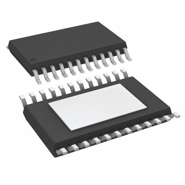
| 供应商器件封装 | 16-SO |
| 其它名称 | 568-4733-1 |
| 内部驱动器 | 是 |
| 功率耗散 | 1 W |
| 包装 | 剪切带 (CT) |
| 参考设计库 | http://designs.digikey.com/library/4294959899/4294959898/464http://designs.digikey.com/library/4294959899/4294959898/512 |
| 商标 | NXP Semiconductors |
| 安装类型 | 表面贴装 |
| 安装风格 | SMD/SMT |
| 封装 | Reel |
| 封装/外壳 | 16-SOIC(0.154",3.90mm 宽) |
| 封装/箱体 | SO-16 |
| 工作温度 | -40°C ~ 100°C |
| 工厂包装数量 | 2500 |
| 恒压 | - |
| 恒流 | - |
| 拓扑 | 回扫,降压(降压) |
| 最大工作温度 | + 100 C |
| 最大电源电流 | 2 mA |
| 最小工作温度 | - 40 C |
| 标准包装 | 1 |
| 电压-电源 | 8.5 V ~ 40 V |
| 电压-输出 | - |
| 相关产品 | /product-detail/zh/750311819/732-2903-ND/2521673/product-detail/zh/750311525/732-2901-ND/2521671/product-detail/zh/750311524/732-2900-ND/2521670/product-detail/zh/750311402/732-2232-ND/2208808/product-detail/zh/750340505/732-2231-ND/2208807 |
| 类型-初级 | 通用 |
| 类型-次级 | - |
| 输入电压 | 8.5 V to 40 V |
| 输出数 | 1 |
| 配用 | /product-detail/zh/SSL2101T%2FDB%2FFBCB120V,598/568-4812-ND/2094727/product-detail/zh/SSL2101T%2FDB%2FFBCB230V,598/568-4811-ND/2094726 |
| 频率 | 10kHz ~ 200kHz |


- 商务部:美国ITC正式对集成电路等产品启动337调查
- 曝三星4nm工艺存在良率问题 高通将骁龙8 Gen1或转产台积电
- 太阳诱电将投资9.5亿元在常州建新厂生产MLCC 预计2023年完工
- 英特尔发布欧洲新工厂建设计划 深化IDM 2.0 战略
- 台积电先进制程称霸业界 有大客户加持明年业绩稳了
- 达到5530亿美元!SIA预计今年全球半导体销售额将创下新高
- 英特尔拟将自动驾驶子公司Mobileye上市 估值或超500亿美元
- 三星加码芯片和SET,合并消费电子和移动部门,撤换高东真等 CEO
- 三星电子宣布重大人事变动 还合并消费电子和移动部门
- 海关总署:前11个月进口集成电路产品价值2.52万亿元 增长14.8%


PDF Datasheet 数据手册内容提取
SSL2101 Dimmable GreenChip driver for LED lighting Rev. 4.1 — 5 December 2011 Product data sheet 1. General description The SSL2101 is a Switched Mode Power Supply (SMPS) driver IC that operates in combination with a phase cut dimmer directly from the rectified mains. It is designed to drive LED devices. The device includes a high-voltage power switch, a circuit to allow start-up directly from the rectified mains voltage and a high-voltage circuitry to supply the phase cut dimmer. For dimmer applications, an integrated dedicated circuitry optimizes the dimming curve. • SSL2101: fully integrated LED driver for lamps up to 10W • SSL2102: fully integrated LED driver for lamps up to 25W • SSL2103: gives the application designer flexibility to: – Use an external power switch to allow the IC to provide any power – Use external bleeder transistors to provide extended dimmer interoperability 2. Features and benefits Easy migration to existing lighting control infrastructure Supports most available dimming solutions Optimized efficiency with valley switching managed by a built-in circuitry Demagnetization detection OverTemperature Protection (OTP) Short-Winding Protection (SWP) and OverCurrent Protection (OCP) Internal V generation allowing start-up from the rectified mains voltage CC Natural dimming curve by logarithmic correction, down to 1% Limited external components required because of the high integration level Thermal enhanced SO16 wide body package Suitable for flyback and buck applications 3. Applications SSL applications below 15W Retro-fit lamps (for example, GU10, E27) LED modules such as LED spots, down-lights LED strings suitable for retail displays, etc.
SSL2101 NXP Semiconductors Dimmable Greenchip driver for LED lighting 4. Quick reference data Table 1: Quick reference data Symbol Parameter Conditions Min Typ Max Unit R drain-source on-state power switch; I =0.50A DSon SOURCE resistance T =25C 4.5 6.5 7.5 j I =0.20A source T =125C - 9.5 10 j V supply voltage 8.5 - 40 V CC f oscillator frequency 10 100 200 kHz osc I current on pin DRAIN V >60V; - - 2.2 mA DRAIN DRAIN noauxiliarysupply V >60V; - 30 125 A DRAIN withauxiliarysupply V voltage on pin DRAIN 40 - 600 V DRAIN minimum duty factor - 0 - % min maximum duty cycle f=100kHz - 75 - % max T ambient temperature 40 - +100 C amb 5. Ordering information Table 2: Ordering info rmation Type number Package Name Description Version SSL2101T SO16 plastic small outline package; 16 leads; body width 3.9 mm SOT109-1 SSL2101 All information provided in this document is subject to legal disclaimers. © NXP B.V. 2011. All rights reserved. Product data sheet Rev. 4.1 — 5 December 2011 2 of 23
SSL2101 NXP Semiconductors Dimmable Greenchip driver for LED lighting 6. Block diagram ISENSE SBLEED WBLEED 10 1 2 BLEEDER 3 16 VCC SUPPLY DRAIN VALLEY 11 AUX 4, 5,13, LOGIC 14, 15 GND 100 mV Stop RC 8 OSCILLATOR 12 SOURCE Low freq Blank THERMAL SHUTDOWN PROTECTION BRIGHTNESS 6 FREQUENCY PORWEESRE -T UP LOGIC 0.5 V REDUCTION RC2 7 CIRCUIT 1.5 V Overcurrent PWM 9 PWMLIMIT LIMIT CIRCUIT Short-winding protection 014aaa567 Fig 1. Block diagram SSL2101 All information provided in this document is subject to legal disclaimers. © NXP B.V. 2011. All rights reserved. Product data sheet Rev. 4.1 — 5 December 2011 3 of 23
SSL2101 NXP Semiconductors Dimmable Greenchip driver for LED lighting 7. Pinning information 7.1 Pinning SBLEED 1 16 DRAIN WBLEED 2 15 GND VCC 3 14 GND GND 4 13 GND SSL2101 GND 5 12 SOURCE BRIGHTNESS 6 11 AUX RC2 7 10 ISENSE RC 8 9 PWMLIMIT 014aaa568 Fig 2. Pin configuration SO16 7.2 Pin description Table 3: Pin description Symbol Pin Description SBLEED 1 drain of internal strong bleeder switch WBLEED 2 drain of internal weak bleeder switch V 3 supply voltage CC GND 4 ground GND 5 ground BRIGHTNESS 6 brightness input RC2 7 setting for frequency reduction RC 8 frequency setting PWMLIMIT 9 PWM limit input ISENSE 10 current sense input for WBLEED AUX 11 Input for voltage from auxiliary winding for timing (demagnetization) SOURCE 12 source of internal power switch GND 13 ground GND 14 ground GND 15 ground DRAIN 16 drain of internal power switch; input for start-up current and valley sensing SSL2101 All information provided in this document is subject to legal disclaimers. © NXP B.V. 2011. All rights reserved. Product data sheet Rev. 4.1 — 5 December 2011 4 of 23
SSL2101 NXP Semiconductors Dimmable Greenchip driver for LED lighting 8. Functional description The SSL2101 is an LED driver IC that operates directly from the rectified mains. The SSL2101 uses on-time mode control and frequency control to control the LED brightness. The BRIGHTNESS and PWMLIMIT input of the IC can be used to control the LED light output in combination with an external dimmer. The PWMLIMIT input can also be used for Thermal Lumen Management (TLM) and for precision LED current control. 8.1 Start-up and UnderVoltage LockOut (UVLO) Initially, the IC is self-supplying from the rectified mains voltage. The IC starts switching as soon as the voltage on pin V passes the V level. The supply can be taken over CC CC(startup) by the auxiliary winding of the transformer as soon as V is high enough and the supply CC from the line is stopped for high efficiency operation. Alternatively the IC can be supplied via a bleeder resistor connected to a high voltage. Note however the maximum V CC voltage rating of the IC. If for some reason the auxiliary supply is not sufficient, the high-voltage supply can also supply the IC. As soon as the voltage on pin V drops below the V level, the IC CC CC(UVLO) stops switching and will restart from the rectified mains voltage, if the internal current delivered is sufficient. 8.2 Oscillator An internal oscillator inside the IC provides the timing for the switching converter logic. The frequency of the oscillator is set by the external resistors and the capacitor on pin RC and pin RC2. The external capacitor is charged rapidly to the V level and, starting RC(max) from a new primary stroke, it discharges to the V level. Because the discharge is RC(min) exponential, the relative sensitivity of the duty factor to the regulation voltage at low duty factor is almost equal to the sensitivity at high duty factors. This results in a more constant gain over the duty factor range compared to Phase Width Modulated (PWM) systems with a linear sawtooth oscillator. Stable operation at low duty factors is easily realized. The frequency of the converter when V is high can be estimated using Equation1: BRIGHTNESS RC = ---1-------1-----–t (1) 3.5 f charge osc R equals the parallel resistance of both oscillator resistors. C is the capacitor connected at the RC pin (pin 8). The BRIGHTNESS input controls the frequency reduction mode. Figure3 shows that the oscillator switches over from an RC curve with R1 in parallel with R2 to R1 only. A low BRIGHTNESS voltage will reduce the switching frequency. SSL2101 All information provided in this document is subject to legal disclaimers. © NXP B.V. 2011. All rights reserved. Product data sheet Rev. 4.1 — 5 December 2011 5 of 23
SSL2101 NXP Semiconductors Dimmable Greenchip driver for LED lighting 5 V STARplug 24 μA OSCILLATOR RC R2 R1 10 kΩ 220 kΩ BRIGHTNESS Comparator C1 330 pF RC2 V V rc_threshold 014aaa574 Fig 3. Brightness control block A typical RC waveform is given in Figure4. The RC switch-over threshold is controlled by the BRIGHTNESS pin. To ensure that the capacitor can be charged within the charge time, the value of the oscillator capacitor should be limited to 1nF. Due to leakage current, the value of the resistor connected between the RC pin and the ground should be limited to a maximum of 220 k. Voltage (mV) RC voltage rc_threshhold 75 mV time 014aaa582 Fig 4. Brightness timing waveform 8.3 Duty factor control The duty factor is controlled by an internally regulated voltage and the oscillator signal on pin RC. The internal regulation voltage is set by the voltage on the PWMLIMIT pin. A low PWMLIMIT voltage will results in a low on-time for the internal power switch. The minimum duty factor of the switched mode power supply can be set to 0 %. The maximum duty factor is set to 75%. SSL2101 All information provided in this document is subject to legal disclaimers. © NXP B.V. 2011. All rights reserved. Product data sheet Rev. 4.1 — 5 December 2011 6 of 23
SSL2101 NXP Semiconductors Dimmable Greenchip driver for LED lighting 8.4 Bleeder for dimming applications The SSL2101 IC contains some circuitry intended for mains dimmer compatibility. This circuit contains two current sinks that are called bleeders. A strong bleeder is used for zero-cross reset of the dimmer and triac latching. A weak bleeder is added to maintain the hold current through the dimmer. The strong bleeder switch is switched on when the maximum voltage on pin WBLEED and SBLEED is below the V level (52 V typically). The weak bleeder switch is th(SBLEED) switched on as soon as the voltage on pin ISENSE exceeds the V level th(high)(ISENSE) (100mV typically). The weak bleeder switch is switched off when the ISENSE voltage drops below the V level (250 mV typically). The weak bleeder switch is also th(low)(ISENSE) switched off when the strong bleeder switch is switched on. See Figure5. WBLEED SBLEED D2 D3 Integrated I1 20 μA B1 M2 LOW V DETECT M1 Q SR −0.1 V OR −0.25 V ISENSE GND 014aaa571 Fig 5. Bleeder circuit 8.5 Valley switching A new cycle is started when the primary switch is switched on (see Figure6). After a time determined by the oscillator voltage, RC and the internal regulation level, the switch is turned off and the secondary stroke starts. The internal regulation level is determined by the voltage on pin PWMLIMIT. After the secondary stroke, the drain voltage shows an oscillation with a frequency of approximately: 1 ---------------------------------------------- (2) 2 L C p p where: L = primary self inductance p C = parasitic capacitance on drain node p SSL2101 All information provided in this document is subject to legal disclaimers. © NXP B.V. 2011. All rights reserved. Product data sheet Rev. 4.1 — 5 December 2011 7 of 23
SSL2101 NXP Semiconductors Dimmable Greenchip driver for LED lighting As soon as the oscillator voltage is high again and the secondary stroke has ended, the circuit waits for a low drain voltage before starting a new primary stroke. Figure6 shows the drain voltage together with the valley signal, the signal indicating the secondary stroke and the RC voltage. The primary stroke starts some time before the actual valley at low ringing frequencies, and some time after the actual valley at high ringing frequencies. primary secondary secondary stroke stroke ringing drain valley secondary stroke A RC regulation level B oscillator 014aaa572 A: Start of new cycle with valley switching. B: Start of new cycle in a classical PWM system. Fig 6. Signals for valley switching, flyback configuration Figure7 shows a typical curve for a reflected output voltage N at an output voltage of 80V. This voltage is the output voltage transferred to the primary side of the transformer with the factor N (determined by the turns ratio of the transformer). It shows that the system switches exactly at minimum drain voltage for ringing frequencies of 480kHz, thus reducing the switch-on losses to a minimum. At 200kHz, the next primary stroke is started at 33 before the valley. The switch-on losses are still reduced significantly. SSL2101 All information provided in this document is subject to legal disclaimers. © NXP B.V. 2011. All rights reserved. Product data sheet Rev. 4.1 — 5 December 2011 8 of 23
SSL2101 NXP Semiconductors Dimmable Greenchip driver for LED lighting 014aaa573 40 phase (°) 20 0 −20 −40 0 200 400 600 800 f (kHz) Fig 7. Typical phase of drain ringing at switch-on (at NV =80V) o 8.6 Demagnetization The system operates in discontinuous conduction mode if the AUX pin is connected. As long as the secondary stroke has not ended, the oscillator will not start a new primary stroke. During the first t seconds, demagnetization recognition is suppressed. sup(xfmr_ring) This suppression may be necessary in applications where the transformer has a large leakage inductance and at low output voltages. 8.7 Overcurrent protection The cycle-by-cycle peak drain current limit circuit uses the external source resistor R SENSE to measure the current. The circuit is activated after the leading edge blanking time t . leb The protection circuit limits the source voltage over the R 1 resistor to V , SENSE th(ocp)SOURCE and thus limits the primary peak current. 8.8 Short-winding protection The short-winding protection circuit is also activated after the leading edge blanking time. If the source voltage exceeds the short-winding protection threshold voltage V , the IC stops switching. Only a power-on reset will restart normal operation. th(swp)SOURCE The short-winding protection also protects in case of a secondary diode short circuit. 8.9 Overtemperature protection Accurate temperature protection is provided in the device. When the junction temperature exceeds the thermal shut-down temperature, the IC stops switching. During thermal protection, the IC current is lowered to the start-up current. The IC continues normal operation as soon as the overtemperature situation has disappeared. 1. R is the resistor between the SOURCE pin and GND SENSE SSL2101 All information provided in this document is subject to legal disclaimers. © NXP B.V. 2011. All rights reserved. Product data sheet Rev. 4.1 — 5 December 2011 9 of 23
SSL2101 NXP Semiconductors Dimmable Greenchip driver for LED lighting 9. Limiting values Table 4: Limiting values In accordance with the Absolute Maximum Rating System (IEC 60134). All voltages are measured with respect to ground; positive currents flow into the device; pins V and RC cannot be current CC driven. Pins ISENSE and AUX cannot be voltage driven. Symbol Parameter Conditions Min Max Unit Voltages V supply voltage continuous 0.4 +40 V CC V voltage on pin RC 0.4 +3 V RC V voltage on pin RC2 0.4 +3 V RC2 V voltage on pin BRIGHTNESS 0.4 +5 V BRIGHTNESS V voltage on pin PWMLIMIT 0.4 +5 V PWMLIMIT V voltage on pin SOURCE 0.4 +5 V SOURCE V voltage on pin DRAIN DMOS power 0.4 +600 V DRAIN transistor; T =25C amb V voltage on pin SBLEED off-state; 0.4 +600 V SBLEED T =125C j on-state; 0.4 +16 V V >8.5V; VCC T <125C j V voltage on pin WBLEED off-state; 0.4 +600 V WBLEED T <125C j on-state; 0.4 +12 V V >8.5V; VCC T <125C j Currents I current on pin ISENSE 20 +5 mA ISENSE I current on pin AUX 10 +5 mA AUX I current on pin SOURCE 2 +2 A SOURCE I current on pin DRAIN 2 +2 A DRAIN General P total power dissipation T =70C - 1 W tot amb T storage temperature 55 +150 C stg T ambient temperature 40 +100 C amb T junction temperature 40 +150 C j SSL2101 All information provided in this document is subject to legal disclaimers. © NXP B.V. 2011. All rights reserved. Product data sheet Rev. 4.1 — 5 December 2011 10 of 23
SSL2101 NXP Semiconductors Dimmable Greenchip driver for LED lighting Table 4: Limiting values …continued In accordance with the Absolute Maximum Rating System (IEC 60134). All voltages are measured with respect to ground; positive currents flow into the device; pins V and RC cannot be current CC driven. Pins ISENSE and AUX cannot be voltage driven. Symbol Parameter Conditions Min Max Unit V electrostatic discharge voltage human body [1] ESD model; Pins16,1,2 1000 +1000 V All other pins 2000 +2000 V machine model [2] 200 +200 V charged device [3] 500 +500 V model [1] Human body model: equivalent to discharging a 100pF capacitor through a 1.5k series resistor. [2] Machine model: equivalent to discharging a 200pF capacitor through a 0.75H coil and a 10 series resistor. [3] Charged device model: equivalent to charging the IC up to 1 kV and the subsequent discharging of each pin down to 0 V over a 1 resistor. 10. Thermal characteristics The heat sink in the application with the SSL2101 is made with the copper on the Printed-Circuit Board (PCB). The SSL2101 uses thermal leads (pins 4, 5, 13, 14 and 15) for heat transfer from die to PCB. Enhanced thermal lead connection may drastically reduce thermal resistance. The following equation shows the relationship between the maximum allowable power dissipation P and the thermal resistance from junction to ambient. R = T –T P thj–a jmax amb Where: R = thermal resistance from junction to ambient th(j-a) T = maximum junction temperature j(max) T = ambient temperature amb P = power dissipation The thermal resistance as a function of the PCB area (Board: 0.8mm thickness, 2 layers, Bottom Cu coverage 90%, Cu thickness 70m (390W/mK), Core material conductivity: 0.5W/mK, 10 vias dia 0.3mm) is shown in Figure8 SSL2101 All information provided in this document is subject to legal disclaimers. © NXP B.V. 2011. All rights reserved. Product data sheet Rev. 4.1 — 5 December 2011 11 of 23
SSL2101 NXP Semiconductors Dimmable Greenchip driver for LED lighting 014aaa811 120 Rth(j-a) (°C/W) 100 80 60 (1) (2) 40 (3) 20 0 2000 4000 6000 8000 10000 PCB area (mm2) (1) Top Cu coverage 20% (2) Top Cu coverage 50% (3) Top Cu coverage 100% Fig 8. SSL2101 core material conductivity T able 5: Thermal characteristics Symbol Parameter Conditions Typ Unit R thermal resistance from junction to ambient [1] 90 KW th(j-a) [1] Measured on a JEDEC test board (standard EIA/JESD 51-3) in free air with natural convection. 11. Characteristics Table 6: Characteristics T =25C; no overtemperature; all voltages are measured with respect to ground; currents are amb positive when flowing into the IC and PWMLIMIT and BRIGHTNESS pins are disconnected unless otherwise specified. Typical frequency 100 kHz. Symbol Parameter Conditions Min Typ Max Unit Supply I supply current normal operation; - 1.7 2 mA CC V =60V; DRAIN V =20V CC I charge supply V >60V; -6 4.5 - mA CC(ch) DRAIN current V =0V CC V supply voltage 8.5 - 40 V CC V start-up supply 9.75 10.25 10.75 V CC(startup) voltage V undervoltage L 7.9 8.2 8.5 V CC(UVLO) lockout supply voltage SSL2101 All information provided in this document is subject to legal disclaimers. © NXP B.V. 2011. All rights reserved. Product data sheet Rev. 4.1 — 5 December 2011 12 of 23
SSL2101 NXP Semiconductors Dimmable Greenchip driver for LED lighting Table 6: Characteristics …continued T =25C; no overtemperature; all voltages are measured with respect to ground; currents are amb positive when flowing into the IC and PWMLIMIT and BRIGHTNESS pins are disconnected unless otherwise specified. Typical frequency 100 kHz. Symbol Parameter Conditions Min Typ Max Unit I current on pin V >60V; - - 2.2 mA DRAIN DRAIN DRAIN noauxiliarysupply V >60V; - 30 125 A DRAIN withauxiliarysupply V voltage on pin 40 - 600 V DRAIN DRAIN Pulse width modulator minimum duty - 0 - % min factor maximum duty f=100kHz - 75 - % max cycle SOPS V demagnetization 50 100 150 mV det(demag) detection voltage t transformer at start of secondary 1.0 1.5 2.0 s sup(xfmr_ring) ringing stroke suppression time RC oscillator V minimum voltage 60 75 90 mV RC(min) on pin RC V maximum voltage 2.4 2.5 2.6 V RC(max) on pin RC t charge time on pin - 1 - s ch(RC) RC V voltage on pin 2.5 V RC2 trip level - 0.5 - V BRIGHTNESS BRIGHTNESS 180 mV RC2 trip level - 1.25 - V 75 mV RC2 trip level - 2.3 - V f oscillator 10 100 200 kHz osc frequency I current on pin V =0V 20 24 28 A BRIGHTNESS BRIGHTNESS BRIGHTNESS Bleeder V threshold voltage 46 52 56 V th(SBLEED) on pin SBLEED V low threshold - 250 - mV th(low)ISENSE voltage on pin ISENSE V high threshold - 100 - mV th(high)ISENSE voltage on pin ISENSE R drain-source I =25 mA DSon(SBLEED) SBLEED on-state T =25C 140 170 200 j resistance on pin SBLEED Tj=125C 220 270 320 SSL2101 All information provided in this document is subject to legal disclaimers. © NXP B.V. 2011. All rights reserved. Product data sheet Rev. 4.1 — 5 December 2011 13 of 23
SSL2101 NXP Semiconductors Dimmable Greenchip driver for LED lighting Table 6: Characteristics …continued T =25C; no overtemperature; all voltages are measured with respect to ground; currents are amb positive when flowing into the IC and PWMLIMIT and BRIGHTNESS pins are disconnected unless otherwise specified. Typical frequency 100 kHz. Symbol Parameter Conditions Min Typ Max Unit R drain-source I = 10 mA DSon(WBLEED) WBLEED on-state T =25C 250 310 350 j resistance on pin WBLEED Tj=125C 400 500 600 Duty factor regulator: pin PWMLIMIT I current on pin 25 - 18 A PWMLIMIT PWMLIMIT V voltage on pin maximum duty cycle = - 3 - V PWMLIMIT PWMLIMIT 3V minimum duty factor - 0.45 - V threshold Valley switching (V/t) valley recognition minimum absolute [1] - 100 - V/s vrec voltage change value with time f ringing frequency NV =100V 200 550 800 kHz ring O t valley recognition - 150 - ns d(vrec-swon) to switch-on delay time Current and short circuit winding protection V overcurrent dV/dt=0.1V/s 0.47 0.50 0.53 V th(ocp)SOURCE protection threshold voltage on pin SOURCE V short-winding dV/dt=0.1V/s - 1.5 - V th(swp)SOURCE protection threshold voltage on pin SOURCE t delay time from dV/dt=0.5V/s - 160 185 ns d(ocp-swoff) overcurrent protection to switch-off t leading edge 250 350 450 ns leb blanking time FET output stage I leakage current on V =600V - - 125 A L(DRAIN) DRAIN pin DRAIN V breakdown T =25C 600 - - V BR(DRAIN) amb voltage on pin DRAIN R drain-source power switch; DSon on-state I =0.50A SOURCE resistance T =25C 4.50 6.5 7.5 j I =0.20A SOURCE T =125C - 9.5 10 j SSL2101 All information provided in this document is subject to legal disclaimers. © NXP B.V. 2011. All rights reserved. Product data sheet Rev. 4.1 — 5 December 2011 14 of 23
SSL2101 NXP Semiconductors Dimmable Greenchip driver for LED lighting Table 6: Characteristics …continued T =25C; no overtemperature; all voltages are measured with respect to ground; currents are amb positive when flowing into the IC and PWMLIMIT and BRIGHTNESS pins are disconnected unless otherwise specified. Typical frequency 100 kHz. Symbol Parameter Conditions Min Typ Max Unit t fall time on pin input voltage: 300V; - 75 - ns f(DRAIN) DRAIN noexternal capacitor at drain Temperature protection T overtemperature junction temperature 150 160 170 C otp protection trip T overtemperature junction temperature - 2 - C otp(hys) protection trip hysteresis [1] Voltage change in time for valley recognition. 100 fmax 80 60 fosc (kHz) 40 20 fmin 0 0 1 2 3 VBRIGHTNESS (V) 014aaa664 Fig 9. Typical frequency as a function of voltage on pin BRIGHTNESS SSL2101 All information provided in this document is subject to legal disclaimers. © NXP B.V. 2011. All rights reserved. Product data sheet Rev. 4.1 — 5 December 2011 15 of 23
SSL2101 NXP Semiconductors Dimmable Greenchip driver for LED lighting 12 ton (μs) 8 4 0 0 1 2 3 VPWMLIMIT (V) 014aaa665 V = 3 V BRIGHTNESS Fig 10. Turn-on time as a function of voltage on pin PWMLIMIT 120 ton (μs) 80 40 0 0 1 2 3 VPWMLIMIT (V) 014aaa666 V = 1 V BRIGHTNESS Fig 11. Turn-on time as a function of voltage on pin PWMLIMIT SSL2101 All information provided in this document is subject to legal disclaimers. © NXP B.V. 2011. All rights reserved. Product data sheet Rev. 4.1 — 5 December 2011 16 of 23
SSL2101 NXP Semiconductors Dimmable Greenchip driver for LED lighting 12. Application information MAINS VCC VCC WBLEED SBLEED VCC DRAIN TLM GND SRC RC SSL2101 AUX VCC RC2 ISENSE BRIGHTNESS PWMLIMIT Dim range 014aaa569 Fig 12. Buck configuration for SSL2101 SSL2101 All information provided in this document is subject to legal disclaimers. © NXP B.V. 2011. All rights reserved. Product data sheet Rev. 4.1 — 5 December 2011 17 of 23
SSL2101 NXP Semiconductors Dimmable Greenchip driver for LED lighting Mains WBLEED SBLEED VCC DRAIN GND SRC RC SSL2101 AUX RC2 ISENSE BRIGHTNESS PWMLIMIT Precision current 014aaa570 Fig 13. Flyback configuration for SSL2101 Further application information can be found in the SSL2101 application notes. SSL2101 All information provided in this document is subject to legal disclaimers. © NXP B.V. 2011. All rights reserved. Product data sheet Rev. 4.1 — 5 December 2011 18 of 23
SSL2101 NXP Semiconductors Dimmable Greenchip driver for LED lighting 13. Package outline SO16: plastic small outline package; 16 leads; body width 3.9 mm SOT109-1 D E A X c y HE v M A Z 16 9 Q A2 A1 (A 3 ) A pin 1 index θ Lp 1 8 L e w M detail X bp 0 2.5 5 mm scale DIMENSIONS (inch dimensions are derived from the original mm dimensions) A UNIT max. A1 A2 A3 bp c D(1) E(1) e HE L Lp Q v w y Z(1) θ 0.25 1.45 0.49 0.25 10.0 4.0 6.2 1.0 0.7 0.7 mm 1.75 0.25 1.27 1.05 0.25 0.25 0.1 0.10 1.25 0.36 0.19 9.8 3.8 5.8 0.4 0.6 0.3 8o 0.010 0.057 0.019 0.0100 0.39 0.16 0.244 0.039 0.028 0.028 0o inches 0.069 0.01 0.05 0.041 0.01 0.01 0.004 0.004 0.049 0.014 0.0075 0.38 0.15 0.228 0.016 0.020 0.012 Note 1. Plastic or metal protrusions of 0.15 mm (0.006 inch) maximum per side are not included. OUTLINE REFERENCES EUROPEAN ISSUE DATE VERSION IEC JEDEC JEITA PROJECTION 99-12-27 SOT109-1 076E07 MS-012 03-02-19 Fig 14. Package outline SOT109-1 (SO16) SSL2101 All information provided in this document is subject to legal disclaimers. © NXP B.V. 2011. All rights reserved. Product data sheet Rev. 4.1 — 5 December 2011 19 of 23
SSL2101 NXP Semiconductors Dimmable Greenchip driver for LED lighting 14. Revision history Table 7: Revision history Document ID Release date Data sheet status Change notice Supersedes SSL2101 v.4.1 20111205 Product data sheet - SSL2101 v.4 Modifications: • GreenChip trademark has been added. • Section 1 “General description” has been updated. • Section 2 “Features and benefits” has been updated. • Section 3 “Applications” has been updated. SSL2101 v.4 20090828 Product data sheet - SSL2101 v.3 SSL2101 v.3 20090525 Product data sheet - SSL2101 v.2 SSL2101 v.2 20090511 Preliminary data sheet - SSL2101 v.1 SSL2101 v.1 20090109 Preliminary data sheet - - SSL2101 All information provided in this document is subject to legal disclaimers. © NXP B.V. 2011. All rights reserved. Product data sheet Rev. 4.1 — 5 December 2011 20 of 23
SSL2101 NXP Semiconductors Dimmable Greenchip driver for LED lighting 15. Legal information 15.1 Data sheet status Document status[1][2] Product status[3] Definition Objective [short] data sheet Development This document contains data from the objective specification for product development. Preliminary [short] data sheet Qualification This document contains data from the preliminary specification. Product [short] data sheet Production This document contains the product specification. [1] Please consult the most recently issued document before initiating or completing a design. [2] The term ‘short data sheet’ is explained in section “Definitions”. [3] The product status of device(s) described in this document may have changed since this document was published and may differ in case of multiple devices. The latest product status information is available on the Internet at URLhttp://www.nxp.com. 15.2 Definitions malfunction of an NXP Semiconductors product can reasonably be expected to result in personal injury, death or severe property or environmental damage. NXP Semiconductors accepts no liability for inclusion and/or use of Draft — The document is a draft version only. The content is still under NXP Semiconductors products in such equipment or applications and internal review and subject to formal approval, which may result in therefore such inclusion and/or use is at the customer’s own risk. modifications or additions. NXP Semiconductors does not give any representations or warranties as to the accuracy or completeness of Applications — Applications that are described herein for any of these information included herein and shall have no liability for the consequences of products are for illustrative purposes only. NXP Semiconductors makes no use of such information. representation or warranty that such applications will be suitable for the specified use without further testing or modification. Short data sheet — A short data sheet is an extract from a full data sheet with the same product type number(s) and title. A short data sheet is intended Customers are responsible for the design and operation of their applications for quick reference only and should not be relied upon to contain detailed and and products using NXP Semiconductors products, and NXP Semiconductors full information. For detailed and full information see the relevant full data accepts no liability for any assistance with applications or customer product sheet, which is available on request via the local NXP Semiconductors sales design. It is customer’s sole responsibility to determine whether the NXP office. In case of any inconsistency or conflict with the short data sheet, the Semiconductors product is suitable and fit for the customer’s applications and full data sheet shall prevail. products planned, as well as for the planned application and use of customer’s third party customer(s). Customers should provide appropriate Product specification — The information and data provided in a Product design and operating safeguards to minimize the risks associated with their data sheet shall define the specification of the product as agreed between applications and products. NXP Semiconductors and its customer, unless NXP Semiconductors and NXP Semiconductors does not accept any liability related to any default, customer have explicitly agreed otherwise in writing. In no event however, damage, costs or problem which is based on any weakness or default in the shall an agreement be valid in which the NXP Semiconductors product is customer’s applications or products, or the application or use by customer’s deemed to offer functions and qualities beyond those described in the third party customer(s). Customer is responsible for doing all necessary Product data sheet. testing for the customer’s applications and products using NXP Semiconductors products in order to avoid a default of the applications and 15.3 Disclaimers the products or of the application or use by customer’s third party customer(s). NXP does not accept any liability in this respect. Limited warranty and liability — Information in this document is believed to Limiting values — Stress above one or more limiting values (as defined in be accurate and reliable. However, NXP Semiconductors does not give any the Absolute Maximum Ratings System of IEC60134) will cause permanent representations or warranties, expressed or implied, as to the accuracy or damage to the device. Limiting values are stress ratings only and (proper) completeness of such information and shall have no liability for the operation of the device at these or any other conditions above those given in consequences of use of such information. the Recommended operating conditions section (if present) or the Characteristics sections of this document is not warranted. Constant or In no event shall NXP Semiconductors be liable for any indirect, incidental, repeated exposure to limiting values will permanently and irreversibly affect punitive, special or consequential damages (including - without limitation - lost the quality and reliability of the device. profits, lost savings, business interruption, costs related to the removal or replacement of any products or rework charges) whether or not such Terms and conditions of commercial sale — NXP Semiconductors damages are based on tort (including negligence), warranty, breach of products are sold subject to the general terms and conditions of commercial contract or any other legal theory. sale, as published at http://www.nxp.com/profile/terms, unless otherwise Notwithstanding any damages that customer might incur for any reason agreed in a valid written individual agreement. In case an individual whatsoever, NXP Semiconductors’ aggregate and cumulative liability towards agreement is concluded only the terms and conditions of the respective customer for the products described herein shall be limited in accordance agreement shall apply. NXP Semiconductors hereby expressly objects to with the Terms and conditions of commercial sale of NXP Semiconductors. applying the customer’s general terms and conditions with regard to the purchase of NXP Semiconductors products by customer. Right to make changes — NXP Semiconductors reserves the right to make changes to information published in this document, including without No offer to sell or license — Nothing in this document may be interpreted or limitation specifications and product descriptions, at any time and without construed as an offer to sell products that is open for acceptance or the grant, notice. This document supersedes and replaces all information supplied prior conveyance or implication of any license under any copyrights, patents or to the publication hereof. other industrial or intellectual property rights. Suitability for use — NXP Semiconductors products are not designed, Export control — This document as well as the item(s) described herein authorized or warranted to be suitable for use in life support, life-critical or may be subject to export control regulations. Export might require a prior safety-critical systems or equipment, nor in applications where failure or authorization from competent authorities. SSL2101 All information provided in this document is subject to legal disclaimers. © NXP B.V. 2011. All rights reserved. Product data sheet Rev. 4.1 — 5 December 2011 21 of 23
SSL2101 NXP Semiconductors Dimmable Greenchip driver for LED lighting Quick reference data — The Quick reference data is an extract of the whenever customer uses the product for automotive applications beyond product data given in the Limiting values and Characteristics sections of this NXP Semiconductors’ specifications such use shall be solely at customer’s document, and as such is not complete, exhaustive or legally binding. own risk, and (c) customer fully indemnifies NXP Semiconductors for any liability, damages or failed product claims resulting from customer design and Non-automotive qualified products — Unless this data sheet expressly use of the product for automotive applications beyond NXP Semiconductors’ states that this specific NXP Semiconductors product is automotive qualified, standard warranty and NXP Semiconductors’ product specifications. the product is not suitable for automotive use. It is neither qualified nor tested in accordance with automotive testing or application requirements. NXP Semiconductors accepts no liability for inclusion and/or use of 15.4 Trademarks non-automotive qualified products in automotive equipment or applications. In the event that customer uses the product for design-in and use in Notice: All referenced brands, product names, service names and trademarks automotive applications to automotive specifications and standards, customer are the property of their respective owners. (a) shall use the product without NXP Semiconductors’ warranty of the GreenChip — is a trademark of NXP B.V. product for such automotive applications, use and specifications, and (b) 16. Contact information For more information, please visit: http://www.nxp.com For sales office addresses, please send an email to: salesaddresses@nxp.com SSL2101 All information provided in this document is subject to legal disclaimers. © NXP B.V. 2011. All rights reserved. Product data sheet Rev. 4.1 — 5 December 2011 22 of 23
SSL2101 NXP Semiconductors Dimmable Greenchip driver for LED lighting 17. Contents 1 General description. . . . . . . . . . . . . . . . . . . . . . 1 2 Features and benefits . . . . . . . . . . . . . . . . . . . . 1 3 Applications. . . . . . . . . . . . . . . . . . . . . . . . . . . . 1 4 Quick reference data. . . . . . . . . . . . . . . . . . . . . 2 5 Ordering information. . . . . . . . . . . . . . . . . . . . . 2 6 Block diagram . . . . . . . . . . . . . . . . . . . . . . . . . . 3 7 Pinning information. . . . . . . . . . . . . . . . . . . . . . 4 7.1 Pinning . . . . . . . . . . . . . . . . . . . . . . . . . . . . . . . 4 7.2 Pin description . . . . . . . . . . . . . . . . . . . . . . . . . 4 8 Functional description . . . . . . . . . . . . . . . . . . . 5 8.1 Start-up and UnderVoltage LockOut (UVLO) . . 5 8.2 Oscillator. . . . . . . . . . . . . . . . . . . . . . . . . . . . . . 5 8.3 Duty factor control . . . . . . . . . . . . . . . . . . . . . . 6 8.4 Bleeder for dimming applications . . . . . . . . . . . 7 8.5 Valley switching . . . . . . . . . . . . . . . . . . . . . . . . 7 8.6 Demagnetization. . . . . . . . . . . . . . . . . . . . . . . . 9 8.7 Overcurrent protection . . . . . . . . . . . . . . . . . . . 9 8.8 Short-winding protection. . . . . . . . . . . . . . . . . . 9 8.9 Overtemperature protection . . . . . . . . . . . . . . . 9 9 Limiting values. . . . . . . . . . . . . . . . . . . . . . . . . 10 10 Thermal characteristics . . . . . . . . . . . . . . . . . 11 11 Characteristics. . . . . . . . . . . . . . . . . . . . . . . . . 12 12 Application information. . . . . . . . . . . . . . . . . . 17 13 Package outline. . . . . . . . . . . . . . . . . . . . . . . . 19 14 Revision history. . . . . . . . . . . . . . . . . . . . . . . . 20 15 Legal information. . . . . . . . . . . . . . . . . . . . . . . 21 15.1 Data sheet status . . . . . . . . . . . . . . . . . . . . . . 21 15.2 Definitions. . . . . . . . . . . . . . . . . . . . . . . . . . . . 21 15.3 Disclaimers. . . . . . . . . . . . . . . . . . . . . . . . . . . 21 15.4 Trademarks. . . . . . . . . . . . . . . . . . . . . . . . . . . 22 16 Contact information. . . . . . . . . . . . . . . . . . . . . 22 17 Contents. . . . . . . . . . . . . . . . . . . . . . . . . . . . . . 23 Please be aware that important notices concerning this document and the product(s) described herein, have been included in section ‘Legal information’. © NXP B.V. 2011. All rights reserved. For more information, please visit: http://www.nxp.com For sales office addresses, please send an email to: salesaddresses@nxp.com Date of release: 5 December 2011 Document identifier: SSL2101