
 Datasheet下载
- 型号: SRV05-4.TCT
- 制造商: SEMTECH
- 库位|库存: xxxx|xxxx
- 要求:
| 数量阶梯 | 香港交货 | 国内含税 |
| +xxxx | $xxxx | ¥xxxx |
查看当月历史价格
查看今年历史价格
SRV05-4.TCT产品简介:
ICGOO电子元器件商城为您提供SRV05-4.TCT由SEMTECH设计生产,在icgoo商城现货销售,并且可以通过原厂、代理商等渠道进行代购。 SRV05-4.TCT价格参考¥1.01-¥1.34。SEMTECHSRV05-4.TCT封装/规格:TVS - 二极管, 17.5V Clamp 12A (8/20µs) Ipp Tvs Diode Surface Mount SOT-23-6。您可以下载SRV05-4.TCT参考资料、Datasheet数据手册功能说明书,资料中有SRV05-4.TCT 详细功能的应用电路图电压和使用方法及教程。
Semtech Corporation的SRV05-4.TCT是一款TVS(瞬态电压抑制)二极管阵列,主要用于保护敏感电子设备免受静电放电(ESD)、电快速瞬变(EFT)和雷击感应等瞬态电压冲击。该器件包含五个双向TVS二极管,采用紧凑的SOT-23-6封装,适用于空间受限的便携式设备。

典型应用场景包括:
1. 通信接口保护:广泛用于USB 2.0、HDMI、RS-232、IEEE 1394等高速数据线路,防止ESD损坏控制器或收发器。
2. 便携式电子产品:如智能手机、平板电脑、笔记本电脑和可穿戴设备,保护连接端口免受日常使用中的静电损伤。
3. 消费类电子设备:应用于机顶盒、数码相机、MP3播放器等人机交互频繁的设备,提升系统可靠性。
4. 工业控制与通信模块:在工控设备的数据接口中提供浪涌保护,增强抗干扰能力。

SRV05-4.TCT具有低电容特性(每通道典型值约1.5pF),确保对高速信号完整性影响最小;其钳位电压低,响应速度快(皮秒级),能有效吸收高达8kV接触ESD(IEC 61000-4-2标准)。此外,器件支持双向保护,适用于交流或双极性信号线路。

综上,SRV05-4.TCT特别适合需要高集成度、小尺寸和高性能ESD防护的现代电子系统,是高速数据端口可靠保护的理想选择。
| 参数 | 数值 |
| 产品目录 | |
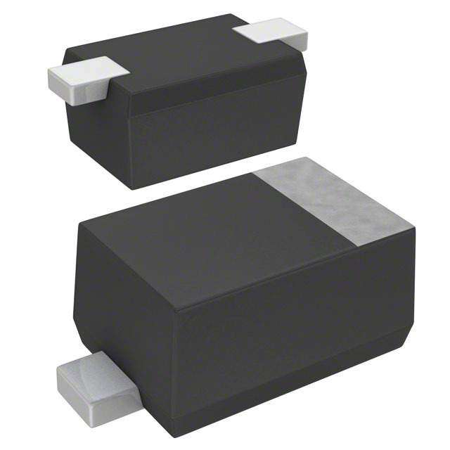
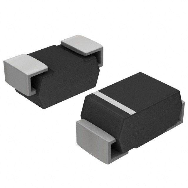
| 描述 | TVS DIODE 5VWM 17.5VC SOT23-6 |
| 产品分类 | |
| 品牌 | Semtech |
| 数据手册 | |
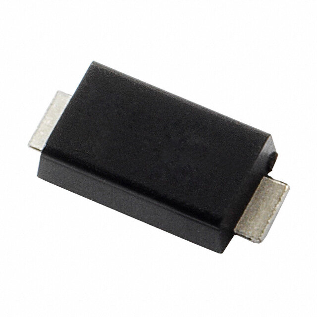
| 产品图片 |
|
| 产品型号 | SRV05-4.TCT |
| PCN组件/产地 | |
| PCN设计/规格 | |
| rohs | 无铅 / 符合限制有害物质指令(RoHS)规范要求 |
| 产品系列 | RailClamp® |
| 不同频率时的电容 | 3pF @ 1MHz |
| 产品目录页面 | |
| 供应商器件封装 | SOT-23-6 |
| 其它名称 | SRV05-4TR |
| 功率-峰值脉冲 | 300W |
| 包装 | 带卷 (TR) |
| 单向通道 | - |
| 双向通道 | 4 |
| 安装类型 | 表面贴装 |
| 封装/外壳 | SOT-23-6 |
| 工作温度 | -55°C ~ 125°C (TJ) |
| 应用 | 通用 |
| 标准包装 | 3,000 |
| 电压-击穿(最小值) | 6V |
| 电压-反向关态(典型值) | 5V(最小值) |
| 电压-箝位(最大值)@Ipp | 17.5V |
| 电流-峰值脉冲(10/1000µs) | 12A (8/20µs) |
| 电源线路保护 | 是 |
| 类型 | 转向装置(轨至轨) |


- 商务部:美国ITC正式对集成电路等产品启动337调查
- 曝三星4nm工艺存在良率问题 高通将骁龙8 Gen1或转产台积电
- 太阳诱电将投资9.5亿元在常州建新厂生产MLCC 预计2023年完工
- 英特尔发布欧洲新工厂建设计划 深化IDM 2.0 战略
- 台积电先进制程称霸业界 有大客户加持明年业绩稳了
- 达到5530亿美元!SIA预计今年全球半导体销售额将创下新高
- 英特尔拟将自动驾驶子公司Mobileye上市 估值或超500亿美元
- 三星加码芯片和SET,合并消费电子和移动部门,撤换高东真等 CEO
- 三星电子宣布重大人事变动 还合并消费电子和移动部门
- 海关总署:前11个月进口集成电路产品价值2.52万亿元 增长14.8%


PDF Datasheet 数据手册内容提取
SRV05-4 RailClamp Low Capacitance TVS Diode Array PROTECTION PRODUCTS Description Features RailClamps are surge rated diode arrays designed to (cid:139) ESD protection for high-speed data lines to protect high speed data interfaces. The SR series has IEC 61000-4-2 (ESD) ±15kV (air), ±8kV (contact) been specifically designed to protect sensitive compo- IEC 61000-4-4 (EFT) 40A (5/50ns) nents which are connected to data and transmission IEC 61000-4-5 (Lightning) 12A (8/20µs) lines from overvoltage caused by electrostatic dis- (cid:139) Array of surge rated diodes with internal TVS Diode charge (ESD), electrical fast transients (EFT), and (cid:139) Small package saves board space lightning. (cid:139) Protects four I/O lines The unique design of the SR series devices incorpo- (cid:139) Low capacitance: 3pF typical rates eight surge rated, low capacitance steering (cid:139) Low clamping voltage diodes and a TVS diode in a single package. During (cid:139) Low operating voltage: 5.0V transient conditions, the steering diodes direct the (cid:139) Solid-state silicon-avalanche technology transient to either the positive side of the power supply Mechanical Characteristics line or to ground. The internal TVS diode prevents over-voltage on the power line, protecting any down- (cid:139) JEDEC SOT-23 6L package stream components. (cid:139) Molding compound flammability rating: UL 94V-0 The SRV05-4 has a low typical capacitance of 3pF and (cid:139) Marking : V05 operates with virtually no insertion loss to 1GHz. This (cid:139) Packaging : Tape and Reel makes the device ideal for protection of high-speed data lines such as USB 2.0, Firewire, DVI, and gigabit Applications Ethernet interfaces. (cid:139) USB 2.0 Power and Data Line Protection The low capacitance array configuration allows the user (cid:139) Video Graphics Cards to protect four high-speed data or transmission lines. (cid:139) Monitors and Flat Panel Displays The low inductance construction minimizes voltage overshoot during high current surges. They may be (cid:139) Digital Video Interface (DVI) used to meet the ESD immunity requirements of IEC (cid:139) 10/100/1000 Ethernet 61000-4-2, Level 4 (±15kV air, ±8kV contact dis- (cid:139) Notebook Computers charge). (cid:139) SIM Ports (cid:139) ATM Interfaces (cid:139) IEEE 1394 Firewire Ports Circuit Diagram Schematic and PIN Configuration 5 1 3 4 6 2 SOT-23 6L (Top View) Revision 01/18/2008 1 www.semtech.com
SRV05-4 PROTECTION PRODUCTS Absolute Maximum Rating Rating Symbol Value Units PeakPulsePower(tp =8/20µs) P 300 Watts pk PeakPulseCurrent (tp =8/20µs) I 12 A PP ESDperIEC61000-4-2(Air) V 15 kV ESD ESDperIEC61000-4-2(Contact) 8 Lead Soldering Temperature T 260(10sec.) °C L Operating Temperature T -55to+125 °C J StorageTemperature T -55to+150 °C STG Electrical Characteristics SRV05-4 Parameter Symbol Conditions Minimum Typical Maximum Units ReverseStand-Off Voltage V Pin 5to2 5 V RWM ReverseBreakdown Voltage V I =1mA 6 V BR t Pin 5to2 ReverseLeakageCurrent I V =5V,T=25°C 5 µA R RWM Pin 5to2 Forward Voltage V I =15mA 1.2 V F f Clamping Voltage V I =1A,tp =8/20µs 12.5 V C PP Any I/Opin toGround Clamping Voltage V I =5A,tp =8/20µs 17.5 V C PP Any I/Opin toGround Junction Capacitance C V =0V,f =1MHz 3 5 pF j R Any I/Opin toGround V =0V,f =1MHz 1.5 pF R Between I/Opins 2008 Semtech Corp. 2 www.semtech.com
SRV05-4 PROTECTION PRODUCTS Typical Characteristics Non-Repetitive Peak Pulse Power vs. Pulse Time Power Derating Curve 10 110 W) 100 ower - P (kPk 1 Power or IPP 67890000 e P ed 50 uls 0.1 Rat 40 ak P % of 30 Pe 20 10 0.01 0 0 25 50 75 100 125 150 0.1 1 10 100 1000 Pulse Duration - tp (µs) Ambient Temperature - TA (oC) Pulse Waveform Clamping Voltage vs. Peak Pulse Current 110 100 Waveform 30.00 Parameters: 90 tr = 8µs V) 25.00 80 td = 20µs (C V of IPP 6700 e-t age - 20.00 ent 50 Volt 15.00 Perc 3400 td = IPP/2 mping 10.00 Waveform a 20 Cl Parameters: 5.00 tr = 8µs 10 td = 20µs 0 0.00 0 5 10 15 20 25 30 0.00 2.00 4.00 6.00 8.00 10.00 12.00 Time (µs) Peak Pulse Current - I (A) PP Forward Voltage vs. Forward Current Normalized Capacitance vs. Reverse Voltage 1.4 7.00 1.2 6.00 V) V (F 5.00 =0) 1 d Voltage - 34..0000 V) / C(VRJR 00..68 orwar 2.00 Waveform C(J 0.4 F Parameters: tr = 8µs 0.2 1.00 td = 20µs f = 1 MHz 0 0.00 0 1 2 3 4 5 0.00 2.00 4.00 6.00 8.00 10.00 12.00 Reverse Voltage - VR (V) Forward Current - I (A) F 2008 Semtech Corp. 3 www.semtech.com
SRV05-4 PROTECTION PRODUCTS Applications Information Insertion Loss S21 Analog Cross Talk CH1 S21 LOG 3 dB/ REF 0 dB CH1 S21 LOG 20 dB/ REF 0 dB START .030 000MHz STOP3000.000000MHz START .030 000MHz STOP3000.000000MHz 2008 Semtech Corp. 4 www.semtech.com
SRV05-4 PROTECTION PRODUCTS Applications Information Data Line and Power Supply Protection Using Vcc as Device Connection Options for Protection of Four reference High-Speed Data Lines The SRV05-4 TVS is designed to protect four data lines from transient over-voltages by clamping them to a fixed reference. When the voltage on the protected line exceeds the reference voltage (plus diode V) the F steering diodes are forward biased, conducting the transient current away from the sensitive circuitry. Data lines are connected at pins 1, 3, 4 and 6. The negative reference (REF1) is connected at pin 2. This pin should be connected directly to a ground plane on the board for best results. The path length is kept as short as possible to minimize parasitic inductance. The positive reference (REF2) is connected at pin 5. The options for connecting the positive reference are as follows: Data Line Protection with Bias and Power Supply Isolation Resistor 1. To protect data lines and the power line, connect pin 5 directly to the positive supply rail (V ). In this CC configuration the data lines are referenced to the supply voltage. The internal TVS diode prevents over-voltage on the supply rail. 2. The SRV05-4 can be isolated from the power supply by adding a series resistor between pin 5 and V . A value of 100kΩ is recommended. The CC internal TVS and steering diodes remain biased, providing the advantage of lower capacitance. 3. In applications where no positive supply reference is available, or complete supply isolation is desired, the internal TVS may be used as the reference. In this case, pin 5 is not connected. The steering diodes will begin to conduct when the voltage on the protected line exceeds the working voltage of Data Line Protection Using Internal TVS Diode as the TVS (plus one diode drop). Reference ESD Protection With RailClamps RailClamps are optimized for ESD protection using the rail-to-rail topology. Along with good board layout, these devices virtually eliminate the disadvantages of using discrete components to implement this topology. Consider the situation shown in Figure 1 where dis- crete diodes or diode arrays are configured for rail-to- rail protection on a high speed line. During positive duration ESD events, the top diode will be forward biased when the voltage on the protected line exceeds 2008 Semtech Corp. 5 www.semtech.com
SRV05-4 PROTECTION PRODUCTS Applications Information (continued) the reference voltage plus the V drop of the diode. F For negative events, the bottom diode will be biased when the voltage exceeds the V of the diode. At first F approximation, the clamping voltage due to the charac- teristics of the protection diodes is given by: PIN Descriptions V = V + V (for positive duration pulses) C CC F V = -V (for negative duration pulses) C F However, for fast rise time transient events, the effects of parasitic inductance must also be consid- ered as shown in Figure 2. Therefore, the actual clamping voltage seen by the protected circuit will be: FFFFFiiiiiggggguuuuurrrrreeeee 11111 ----- “““““RRRRRaaaaaiiiiilllll-----TTTTTooooo-----RRRRRaaaaaiiiiilllll””””” PPPPPrrrrrooooottttteeeeeccccctttttiiiiiooooonnnnn TTTTTooooopppppooooolllllooooogggggyyyyy V = V + V + L di /dt (for positive duration pulses) (((((FFFFFiiiiirrrrrsssssttttt AAAAApppppppppprrrrroooooxxxxxiiiiimmmmmaaaaatttttiiiiiooooonnnnn))))) C CC F P ESD V = -V - L di /dt (for negative duration pulses) C F G ESD ESD current reaches a peak amplitude of 30A in 1ns for a level 4 ESD contact discharge per IEC 61000-4-2. Therefore, the voltage overshoot due to 1nH of series inductance is: V = L di /dt = 1X10⁻⁹ (30 / 1X10⁻⁹) = 30V P ESD Example: Consider a V = 5V, a typical V of 30V (at 30A) for the CC F steering diode and a series trace inductance of 10nH. The clamping voltage seen by the protected IC for a positive 8kV (30A) ESD pulse will be: FFFFFiiiiiggggguuuuurrrrreeeee 22222 ----- TTTTThhhhheeeee EEEEEffffffffffeeeeeccccctttttsssss ooooofffff PPPPPaaaaarrrrraaaaasssssiiiiitttttiiiiiccccc IIIIInnnnnddddduuuuuccccctttttaaaaannnnnccccceeeee WWWWWhhhhheeeeennnnn UUUUUsssssiiiiinnnnnggggg DDDDDiiiiissssscccccrrrrreeeeettttteeeee CCCCCooooommmmmpppppooooonnnnneeeeennnnntttttsssss tttttooooo IIIIImmmmmpppppllllleeeeemmmmmeeeeennnnnttttt V = 5V + 30V + (10nH X 30V/nH) = 335V C RRRRRaaaaaiiiiilllll-----TTTTTooooo-----RRRRRaaaaaiiiiilllll PPPPPrrrrrooooottttteeeeeccccctttttiiiiiooooonnnnn This does not take into account that the ESD current is directed into the supply rail, potentially damaging any components that are attached to that rail. Also note that it is not uncommon for the V of discrete diodes to F exceed the damage threshold of the protected IC. This is due to the relatively small junction area of typical discrete components. It is also possible that the power dissipation capability of the discrete diode will be exceeded, thus destroying the device. The RailClamp is designed to overcome the inherent disadvantages of using discrete signal diodes for ESD suppression. The RailClamp’s integrated TVS diode FFFFFiiiiiggggguuuuurrrrreeeee 33333 ----- RRRRRaaaaaiiiiilllll-----TTTTTooooo-----RRRRRaaaaaiiiiilllll PPPPPrrrrrooooottttteeeeeccccctttttiiiiiooooonnnnn UUUUUsssssiiiiinnnnnggggg RRRRRaaaaaiiiiilllllCCCCClllllaaaaammmmmppppp TTTTTVVVVVSSSSS AAAAArrrrrrrrrraaaaayyyyysssss 2008 Semtech Corp. 6 www.semtech.com
SRV05-4 PROTECTION PRODUCTS Applications Information (continued) helps to mitigate the effects of parasitic inductance in the power supply connection. During an ESD event, the current will be directed through the integrated TVS diode to ground. The maximum voltage seen by the protected IC due to this path will be the clamping voltage of the device. Video Interface Protection Video interfaces are susceptible to transient voltages resulting from electrostatic discharge (ESD) and “hot plugging” cables. If left unprotected, the video interface IC may be damaged or even destroyed. Protecting a high-speed video port presents some unique challenges. First, any added protection device must have extremely low capacitance and low leakage current so that the integrity of the video signal is not compromised. Second, the protection component must be able to absorb high voltage transients without Figure 4 - Video Interface Protection damage or degradation. As a minimum, the device should be rated to handle ESD voltages per IEC 61000-4-2, level 4 (±15kV air, ±8kV contact). The clamping voltage of the device (when conducting high current ESD pulses) must be sufficiently low enough to protect the sensitive CMOS IC. If the clamping voltage SRV05-4 is too high, the “protected” device may latch-up or be destroyed. Finally, the device must take up a relatively small amount of board space, particularly in portable applications such as notebooks and handhelds. The SRV05-4 is designed to meet or exceed all of the above criteria. A typical video interface protection circuit is shown in Figure 4. All exposed lines are protected including R, G, B, H-Sync, V-Sync , and the ID lines for plug and play monitors. Figure 5 - Dual USB Port Protection Universal Serial Bus ESD Protection The SRV05-4 may also be used to protect the USB ports on monitors, computers, peripherals or portable systems. Each device will protect up to two USB ports (Figure 5). When the voltage on the data lines exceed the bus voltage (plus one diode drop), the internal rectifiers are forward biased conducting the transient current away from the protected controller chip. The TVS diode directs the surge to ground. The TVS diode also acts to suppress ESD strikes directly on the voltage bus. Thus, both power and data pins are protected with a single device. Figure 6 - SIM Port 2008 Semtech Corp. 7 www.semtech.com
SRV05-4 PROTECTION PRODUCTS DVI Protection 10/100 ETHERNET PROTECTION The small geometry of a typical digital-visual interface Ethernet ICs are vulnerable to damage from electro- (DVI) graphic chip will make it more susceptible to static discharge (ESD). The internal protection in the electrostatic discharges (ESD) and cable discharge PHY chip, if any, often is not enough due to the high events (CDE). Transient protection of a DVI port can energy of the discharges specified by IEC 61000-4-2. be challenging. Digital-visual interfaces can often If the discharge is catastrophic, it will destroy the transmit and receive at a rate equal to or above protected IC. If it is less severe, it will cause latent 1Gbps. The high-speed data transmission requires the failures that are very difficult to find. protection device to have low capacitance to maintain signal integrity and low clamping voltage to reduce 10/100 Ethernet operates at 125MHz clock over a stress on the protected IC. The SRV05-4 has a low twisted pair interface. In a typical system, the twisted- typical insertion loss of <0.4dB at 1GHz (I/O to ground) pair interface for each port consists of two differential to ensure signal integrity and can protect the DVI signal pairs: one for the transmitter and one for the interface to the 8kV contact and 15kV air ESD per IEC receiver, with the transmitter input being the most 61000-4-2 and CDE. sensitive to damage. The fatal discharge occurs differentially across the transmit or receive line pair Figure 7 shows how to design the SRV05-4 into the and is capacitively coupled through the transformer to DVI circuit on a flat panel display and a PC graphic the Ethernet chip. Figure 8 shows how to design the card. The SRV05-4 is configured to provide common SRV05-4 on the line side of a 10/100 ethernet port to mode and differential mode protection. The internal provide differential mode protection. The common TVS of the SRV05-4 acts as a 5 volt reference. The mode isolation of the transformer will provide common power pin of the DVI circuit does not come out through mode protection to the rating of the transformer the connector and is not subjected to external ESD isolation which is usually >1.5kV. If more common pulse; therefore, pin 5 should be left unconnected. mode protection is needed, figure 9 shows how to Connecting pin 5 to Vcc of the DVI circuit may result in design the SRV05-4 on the IC side of the 10/100 damage to the chip from ESD current. Figure 7 - Digital Video Interface (DVI) Protection 2008 Semtech Corp. 8 www.semtech.com
SRV05-4 PROTECTION PRODUCTS SRV05-4 Figure 8 - 10/100 Ethernet Differential Protection Figure 9 - 10/100 Ethernet Differential and Common Mode Protection 2008 Semtech Corp. 9 www.semtech.com
SRV05-4 PROTECTION PRODUCTS 10/100 ETHERNET PROTECTION CONT’ Ethernet circuit to provide differential and common mode protection. The SRV05-4 can not be grounded on the line side because the hi-pot test requires the line side not to be grounded. 2008 Semtech Corp. 10 www.semtech.com
SRV05-4 PROTECTION PRODUCTS Applications Information - SPICE Model nH SRV05-4 Spice Model SRV05-4Spice Parameters Parameter Unit D1(LCRD) D2(LCRD) D3(TVS) IS Amp 10E-14 10E-14 10E-14 BV Volt 180 20 8.59 VJ Volt 0.62 0.59 0.6 RS Ohm 0.31 0.37 0.500 IBV Amp 1E-3 1E-3 1E-3 CJO Farad 3E-12 1E-12 360E-12 TT sec 2.541E-9 2.541E-9 2.541E-9 M -- 0.01 0.01 0.334 N -- 1.1 1.1 1.1 EG eV 1.11 1.11 1.11 2008 Semtech Corp. 11 www.semtech.com
SRV05-4 PROTECTION PRODUCTS OOuuttlliinnee DDrraawwiinngg --S SOOT-283 6L DIMENSIONS INCHES MILLIMETERS A DIM MIN NOMMAX MIN NOMMAX e1 D A .035 - .057 0.90 - 1.45 A1 .000 - .006 0.00 - 0.15 A2 .035 .045 .051 .90 1.15 1.30 N b .010 - .020 0.25 - 0.50 2X E/2 c .003 - .009 0.08 - 0.22 EI E D .110 .114 .122 2.80 2.90 3.10 E1 .060 .063 .069 1.50 1.60 1.75 1 2 E .110 BSC 2.80 BSC ccc C e .037 BSC 0.95 BSC 2X N/2 TIPS e1 .075 BSC 1.90 BSC e L .012 .018 .024 0.30 0.45 0.60 L1 (.024) (0.60) B N 6 6 01 0° - 10° 0° - 10° aaa .004 0.10 bbb .008 0.20 D ccc .008 0.20 aaa C A2 A SEATING PLANE H C A1 bxN GAGE c bbb C A-B D PLANE 0.25 L 01 (L1) DETAIL A SEE DETAIL A SIDE VIEW NOTES: 1. CONTROLLING DIMENSIONS ARE IN MILLIMETERS (ANGLES IN DEGREES). 2. DATUMS - A - AND - B - TO BE DETERMINED AT DATUM PLANE-H- 3. DIMENSIONS "E1" AND "D" DO NOT INCLUDE MOLD FLASH, PROTRUSIONS OR GATE BURRS. Land Pattern -SOT23 6L X DDIIMMEENNSSIIOONNSS DDIIMM IINNCCHHEESS MMIILLLLIIMMEETTEERRSS CC (.098) (2.50) GG .055 1.40 (C) G Z PP .037 0.95 Y XX .024 0.60 YY .043 1.10 ZZ .141 3.60 P NOTES: 1. THIS LAND PATTERN IS FOR REFERENCE PURPOSES ONLY. CONSULT YOUR MANUFACTURING GROUP TO ENSURE YOUR COMPANY'S MANUFACTURING GUIDELINES ARE MET. 2008 Semtech Corp. 12 www.semtech.com
SRV05-4 PROTECTION PRODUCTS Marking Codes Ordering Information Part Qtyper Lead Finish ReelSize Number Reel V05 SRV05-4.TC SnPb 3,000 7Inch SRV05-4.TCT Pb free 3,000 7Inch Marking Part Number Code SRV05-4 V05 Tape and Reel Specification User Direction of feed A0 B0 K0 3.23+/-0.05mm 3.17+/-0.05mm 1.37+/-0.05mm Tape K B,(Max) D D1 E F P P0 P2 T(MAX) W Width (MAX) 8.0mm 1.0mm 1.750±.10 4.2mm 1.5+0.1mm 3.5±0.05 4.0±0.1 4.0±0.1 2.0±0.05 +0.3mm 8mm ±0.05 mm 2.4mm 0.4mm (.165) -0.0mm mm mm mm mm -0.1mm Contact Information Semtech Corporation Protection Products Division 200 Flynn Road, Camarillo, CA 93012 Phone: (805)498-2111 FAX (805)498-3804 2008 Semtech Corp. 13 www.semtech.com