ICGOO在线商城 > SQL48T20033-NDABG

 Datasheet下载
- 型号: SQL48T20033-NDABG
- 制造商: Power-One
- 库位|库存: xxxx|xxxx
- 要求:
| 数量阶梯 | 香港交货 | 国内含税 |
| +xxxx | $xxxx | ¥xxxx |
查看当月历史价格
查看今年历史价格
SQL48T20033-NDABG产品简介:
ICGOO电子元器件商城为您提供SQL48T20033-NDABG由Power-One设计生产,在icgoo商城现货销售,并且可以通过原厂、代理商等渠道进行代购。 提供SQL48T20033-NDABG价格参考¥147.44-¥168.67以及Power-OneSQL48T20033-NDABG封装/规格参数等产品信息。 你可以下载SQL48T20033-NDABG参考资料、Datasheet数据手册功能说明书, 资料中有SQL48T20033-NDABG详细功能的应用电路图电压和使用方法及教程。
| 参数 | 数值 |
| 产品目录 | |
| 描述 | CONV DC-DC 3.3V 20A 1/8 BRICK隔离式DC/DC转换器 3.3V at 20A baseplate |
| 产品分类 | DC DC ConvertersDC/DC转换器 |
| 品牌 | Bel Power Solutions |
| 产品手册 | |
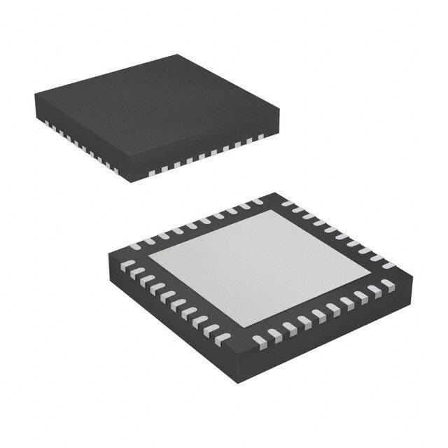
| 产品图片 |
|
| rohs | 符合RoHS无铅 / 符合限制有害物质指令(RoHS)规范要求 |
| 产品系列 | 隔离式DC/DC转换器,Bel Power Solutions SQL48T20033-NDABGSQL48T20033 |
| 数据手册 | |
| 产品型号 | SQL48T20033-NDABG |
| 产品 | Isolated |
| 产品种类 | 隔离式DC/DC转换器 |
| 其它名称 | 179-2427 |
| 功率(W)-制造系列 | 66W |
| 功率(W)-最大值 | 66W |
| 包装 | 散装 |
| 商标 | Bel Power Solutions |
| 大小/尺寸 | 2.30" 长 x 0.90" 宽 x 0.52" 高(58.4mm x 22.8mm x 13.1mm) |
| 安装类型 | 通孔 |
| 安装风格 | Chassis |
| 宽度 | 0.9 in |
| 封装/外壳 | 8-DIP 模块,1/8 砖 |
| 封装/箱体尺寸 | 1/8 Brick |
| 尺寸 | 2.3 in x 0.9 in x 0.5 in |
| 工作温度 | -40°C ~ 85°C |
| 效率 | 91% |
| 标准包装 | 200 |
| 特性 | 具有远程开/关功能和 UVLO |
| 电压-输入(最大值) | 75V |
| 电压-输入(最小值) | 36V |
| 电压-输出1 | 3.3V |
| 电压-输出2 | - |
| 电压-输出3 | - |
| 电压-隔离 | 2.25kV(2250V) |
| 电流-输出(最大值) | 20A |
| 相关产品 | /product-detail/zh/ATS-1178-C1-R0/ATS1489-ND/4146472/product-detail/zh/ATS-1179-C1-R0/ATS1512-ND/4146473/product-detail/zh/ATS-1181-C1-R0/ATS1491-ND/4146474/product-detail/zh/ATS-1183-C1-R0/ATS1492-ND/4146475/product-detail/zh/ATS-1184-C1-R0/ATS1493-ND/4146476/product-detail/zh/ATS-1186-C1-R0/ATS1494-ND/4146477 |
| 类型 | 隔离模块 |
| 绝缘电压 | 2.25 kV |
| 输入电压—公称值 | 48 V |
| 输入电压范围 | 36 V to 75 V |
| 输出数 | 1 |
| 输出电压—通道1 | 3.3 V |
| 输出电流—通道1 | 20 A |
| 输出端数量 | 1 |
| 输出类型 | Isolated |
| 长度 | 2.3 in |
| 高度 | 0.5 in |


- 商务部:美国ITC正式对集成电路等产品启动337调查
- 曝三星4nm工艺存在良率问题 高通将骁龙8 Gen1或转产台积电
- 太阳诱电将投资9.5亿元在常州建新厂生产MLCC 预计2023年完工
- 英特尔发布欧洲新工厂建设计划 深化IDM 2.0 战略
- 台积电先进制程称霸业界 有大客户加持明年业绩稳了
- 达到5530亿美元!SIA预计今年全球半导体销售额将创下新高
- 英特尔拟将自动驾驶子公司Mobileye上市 估值或超500亿美元
- 三星加码芯片和SET,合并消费电子和移动部门,撤换高东真等 CEO
- 三星电子宣布重大人事变动 还合并消费电子和移动部门
- 海关总署:前11个月进口集成电路产品价值2.52万亿元 增长14.8%


PDF Datasheet 数据手册内容提取
The new high performance 20 A SQL48T20033 DC-DC converter provides a high efficiency single output, in a 1/8th brick package that is only 62% the size of the industry-standard quarter-brick. Specifically designed for operation in systems that have limited airflow and increased ambient temperatures, the SQL48T20033 converter utilizes the same pin-out and Input / Output functionality of the industry-standard quarter-bricks. In addition, a heat spreader feature is available (-xxxBx suffix) that provides an effective thermal interface for coldplate and heat sinking options. The SQL48T20033 converter thermal performance is accomplished through the use of patent-pending circuits, packaging, and processing techniques to achieve ultra-high efficiency, excellent thermal management, and a low-body profile. Low-body profile and the preclusion of heat sinks minimize impedance to system airflow, thus enhancing cooling for both upstream and downstream devices. The use of 100% automation for assembly, coupled with advanced electronic circuits and thermal design, results in a product with extremely high reliability. Operating from a wide-range 36-75 V input, the SQL48T20033 converter provides a fully regulated 3.3 V output voltage. The outputs can be trimmed from –20% to +10% of the nominal output voltage, thus providing outstanding design flexibility. Employing a standard power pin-out, the SQL48T20033 converter is an ideal drop-in replacement for existing high current quarter- brick designs. Inclusion of this converter in a new design can result in significant board space and cost savings. The designer can expect reliability improvement over other available converters because of the SQL48T20033’s optimized thermal efficiency. 36-75 VDC Input; 3.3 VDC @ 20 A Output with no derating up to 70°C (@ 48 Vin, ≥ 100 LFM) Withstands 100 V input transient for 100ms Fixed-frequency operation On-board input differential LC-filter Start-up into pre-biased load No minimum load required Fully protected (OTP, OCP, OVP, UVLO) Remote output sense Positive or negative logic ON/OFF option Output voltage trim range: +10%/−20% with Industry Standard trim equations Low height of 0.375” (9.5 mm) Approved to the latest edition of the following standards: UL/CSA60950-1, IEC60950-1 and EN60950-1. All materials meet UL94, V-0 flammability rating RoHS lead-free solder and lead-solder-exempted products are available Telecommunications, Data communications / processing, LAN/WAN, Servers, Workstations
SQL48T20033 2 Conditions: TA = 25 ºC, Airflow = 300 LFM (1.5 m/s), Vin = 48 VDC, unless otherwise specified. PARAMETER CONDITIONS / DESCRIPTION MIN TYP MAX UNITS Absolute Maximum Ratings Continuous -0.3 80 VDC Input Voltage Transient (100ms) 100 VDC Operating Temperature 1 Ambient (TA) -40 85 °C Component (TC) -40 120 °C (See Derating Curves) Baseplate (TB) -40 105 °C Storage Temperature -55 125 °C Isolation Characteristics I/O Isolation 2,250 VDC Isolation Capacitance 270 pF Isolation Resistance 10 MΩ Input to Baseplate 1,500 VDC Output to Baseplate 1,500 VDC Feature Characteristics Switching Frequency 445 kHz Output Voltage Trim Range 2 Industry-std. equations3 -20 +10 % Remote Sense Compensation 2, 4 Percent of VOUT(NOM) +10 % Output Overvoltage Protection Non-latching 120 140 % Over Temperature Shutdown Non-latching 125 °C Auto-Restart Period Applies to all protection features 200 ms Turn-On Time from Vin Time from UVLO to Vo = 90%VOUT(NOM) 5 20 ms Resistive Load Turn-On Time from ON/OFF Control Time from ON to Vo = 90% VOUT(NOM) 5 20 ms Resistive Load Converter Off (logic low) -20 0.8 VDC ON/OFF Control (Positive Logic option) Converter On (logic high) 2.4 20 VDC Converter Off (logic high) 2.4 20 VDC ON/OFF Control (Negative Logic option) Converter On (logic low) -20 0.8 VDC Input Characteristics Operating Input Voltage Range 36 48 75 VDC Turn-on Threshold 31.5 33.5 35.5 VDC Input Undervoltage Lockout Turn-off Threshold 30 32 34 VDC Lockout Hysteresis Voltage 1.0 2.0 VDC 1 Reference Figure H for component (TC and TB) locations. 2 Vout can be increased up to 10% via the sense leads or up to 10% via the trim function. However, the total output voltage trim-up should not exceed 10% of VOUT(NOM). 3 Trim equations are defined within this document’s “Operations” section. 4 When using remote sense a minimum of 100uF ceramic capacitance should be mounted between Vout(+) and Vout(-) close to pin 8 and pin 4. tech.support@psbel.com
SQL48T20033 3 Maximum Input Current 3.3 Vout, Full Load @ 36 VDC In 2.1 ADC Input Standby Current Vin = 48V, converter disabled 5 mADC Input No Load Current (No load on the output) Vin = 48V, converter enabled 45 mADC 200 400 mAPK-PK Input Reflected-Ripple Current, ic Vin = 48 V, 20 MHz bandwidth, 150 mARMS Full Load (resistive) (See Fig. J) 30 mAPK-PK Input Reflected-Ripple Current, iS 5 mARMS Input Voltage Ripple Rejection @ 120 Hz 60 dB Output Characteristics Output Voltage Setpoint VIN = 48 V, IOUT = 0 Amps, TA = 25°C 3.25 3.3 3.35 VDC Over Line: IOUT = 20Amps, TA = 25°C ±2 ±17 mV Output Regulation Over Load: VIN=48V, , TA=25°C ±2 ±17 mV Output Voltage Range Over line, load and temperature 3.2 3.4 VDC Output Ripple and Noise – 20 MHz bandwidth IOUT = 20 Amps, 30 100 mVPK-PK CEXT =10 µF tantalum + 1 µF ceramic 15 30 VRMS External Load Capacitance1 Plus Full Load (resistive) CEXT 0 10,000 µF ESR 1 mOhm Output Current Range 0 20 ADC Current Limit Inception Non-latching 22 26 30 ADC Short-Circuit Current Pk: 30 Amps Non-latching Short = 10 mΩ RMS: 5 10 ARMS Dynamic Response di/dt = 0.1 A/μs ±50 mV Load Change 50%-75%-50% of IOUT Max CdiE/XdTt == 110.0µ FA /tμasn t a lum + 1µF ceramic ±100 mV CEXT = 470µF POS + 1µF ceramic Settling Time to 1% of VOUT 20 µs Efficiency @ 100% Load 48V 91 % @ 50% Load IN, TA = 25°C, 300LFM (1.5 m/s) 90 % Environmental Operating Humidity RH (Non-condensing) 95 % Storage Humidity RH (Non-condensing) 95 % Mechanical No Baseplate 21.4 g Weight With Baseplate 32.9 g Reliability Telcordia SR-332, Method I Case 1 50% MTBF 23.6 MHrs electrical stress, 40°C components EMI and Regulatory Compliance Conducted Emissions CISPR 22 B with external EMI filter network UL60950-1/CSA60950-1, EN60950-1 and Safely Agency Approvals IEC60950-1 Asia-Pacific Europe, Middle East North America +86 755 298 85888 +353 61 225 977 +1 408 785 5200 © 2016 Bel Power Solutions & Protection BCD.00730_AB
SQL48T20033 4 These power converters have been designed to be stable with no external capacitors when used in low inductance input and output circuits. In many applications, the inductance associated with the distribution from the power source to the input of the converter can affect the stability of the converter. The addition of a 33 μF electrolytic capacitor with an ESR <1 Ω across the input helps to ensure stability of the converter. In applications where decoupling capacitance is distributed at the load, the power converter will exhibit stable operation with up to the maximum admissible external load capacitance up to 10,000 µF and ESR > 1mΩ. The ON/OFF pin is used to turn the power converter on or off remotely via a system signal. There are two remote control options available, positive and negative logic, with both referenced to Vin(-). A typical connection is shown in Fig. A. Vin (+) SQL 48 Converter Vout (+) ( T op View ) SENSE (+) ON / O FF TRIM Rload Vin SENSE (-) Vin ( - ) Vout ( - ) CONTRO L INPUT Figure A. Circuit configuration for ON/OFF function. The positive logic version turns on when the ON/OFF pin is at logic high and turns off when at logic low. The converter is on when the ON/OFF pin is left open. See the Electrical Specifications for logic high/low definitions. The negative logic version turns on when the pin is at logic low and turns off when the pin is at logic high. The ON/OFF pin can be hard wired directly to Vin(-) to enable automatic power up of the converter without the need of an external control signal. The ON/OFF pin is internally pulled up to 5 VDC through a resistor. A properly de-bounced mechanical switch, open-collector transistor, or FET can be used to drive the input of the ON/OFF pin. The device must be capable of sinking up to 0.2 mA at a low level voltage of ≤ 0.8 V. An external voltage source (±20 V maximum) may be connected directly to the ON/OFF input, in which case it must be capable of sourcing or sinking up to 1 mA depending on the signal polarity. See the Startup Information section for system timing waveforms associated with use of the ON/OFF pin. The remote sense feature of the converter compensates for voltage drops occurring between the output pins of the converter and the load. The SENSE(-) (Pin 5) and SENSE(+) ( Pin 7) pins should be connected at the load or at the point where regulation is required (see Fig. B). When using remote sense a minimum of 100uF ceramic capacitance should be mounted between Vout(+) and Vout(-) close to the pin 8 and pin 4. Vin (+) SQL 48 Conv e rter Vout (+) Rw (Top View) 100 SENSE (+) Vin ON/OFF SENSET R IM( - ) Rload Vin ( - ) Vout 1( 0 -) Rw Figure B. Remote sense circuit configuration. tech.support@psbel.com
SQL48T20033 5 CAUTION If remote sensing is not utilized, the SENSE(-) pin must be connected to the Vout(-) pin, and the SENSE(+) pin must be connected to the Vout(+) pin to ensure the converter will regulate at the specified output voltage. If these connections are not made, the converter will deliver an output voltage that is slightly higher than the specified data sheet value. Because the sense leads carry minimal current, large traces on the end-user board are not required. However, sense traces should be run side by side and located close to a ground plane to minimize system noise and ensure optimum performance. The converter’s output overvoltage protection (OVP) circuitry senses the voltage across Vout(+) and Vout(-), and not across the sense lines, so the resistance (and resulting voltage drop) between the output pins of the converter and the load should be minimized to prevent unwanted triggering of the OVP. When utilizing the remote sense feature, care must be taken not to exceed the maximum allowable output power capability of the converter, which is equal to the product of the nominal output voltage and the allowable output current for the given conditions. When using remote sense, the output voltage at the converter can be increased by as much as 10% above the nominal rating in order to maintain the required voltage across the load. Therefore, the designer must, if necessary, decrease the maximum current (originally obtained from the derating curves) by the same percentage to ensure the converter’s actual output power remains at or below the maximum allowable output power. The output voltage can be adjusted up 10% or down 20% relative to the rated output voltage by the addition of an externally connected resistor. For output voltage 3.3V, trim-up to 10% is guaranteed at Vin ≥ 40V, and to 8% at Vin ≥ 36V. The TRIM pin should be left open if trimming is not being used. To minimize noise pickup, a 0.1 µF capacitor is connected internally between the TRIM and SENSE(-) pins. To increase the output voltage (Fig. C) a trim resistor, RT-INCR, should be connected between the TRIM (Pin 6) and SENSE(+) (Pin 7), with a value of 5.11(100Δ)V 626 ONOM R 10.22 TINCR 1.225Δ [kΩ], where, RTINCR Required value of trim-up resistor kΩ] VONOM Nominal value of output voltage [V] (VO-REQVO-NOM) Δ X 100 VO -NOM [%] VOREQ Desired (trimmed) output voltage [V]. When trimming up, care must be taken not to exceed the converter‘s maximum allowable output power. See the previous section for a complete discussion of this requirement. Vin (+) SQL (4 T 8 o p C Voienwve ) r t er Vou t (+) Vin ON / O FF SENSET RIM(+ ) R T - IN CR Rload SENSE (-) Vin(-) Vout (-) Figure C. Configuration for increasing output voltage. To decrease the output voltage (Fig. D), a trim resistor, RT-DECR, should be connected between the TRIM (Pin 6) and SENSE(-) (Pin 5), with a value of: Asia-Pacific Europe, Middle East North America +86 755 298 85888 +353 61 225 977 +1 408 785 5200 © 2016 Bel Power Solutions & Protection BCD.00730_AB
SQL48T20033 6 511 R 10.22 TDECR |Δ| [kΩ] where, RTDECR Δ Required value of trim-down resistor [kΩ] and is defined above. Note: The above equations for calculation of trim resistor values match those typically used in conventional industry-standard quarter-bricks, eighth-bricks and sixteenth-brick models. Vin (+) SQL 48 Converter Vout (+) (Top View) SENSE (+) Vin ON / O FF SENSTER I M( - ) R T - D E CR Rload Vin ( - ) Vout ( - ) Figure D. Configuration for decreasing output voltage. Trimming/sensing beyond 110% of the rated output voltage is not an acceptable design practice, as this condition could cause unwanted triggering of the output overvoltage protection (OVP) circuit. The designer should ensure that the difference between the voltages across the converter’s output pins and its sense pins does not exceed 10% of VOUT(nom), or: [VOUT()VOUT()][VSENSE()VSENSE()] VO-NOM X 10% [V] This equation is applicable for any condition of output sensing and/or output trim. tech.support@psbel.com
SQL48T20033 7 Input undervoltage lockout is standard with this converter. The converter will shut down when the input voltage drops below a pre-determined voltage. The input voltage must be typically 34 V for the converter to turn on. Once the converter has been turned on, it will shut off when the input voltage drops typically below 32 V. This feature is beneficial in preventing deep discharging of batteries used in telecom applications. All output circuit protection features are non-latching and operate in a “hiccup” mode. After an output protection event occurs, the converter will be turned off, and held off for approximately 200 ms after which, the protection circuit will reset and the converter will attempt to restart. If the fault is still present, the converter will repeat the above action. Once the fault is removed, the converter will start normally The converter is protected against overcurrent or short circuit conditions. Upon sensing an overcurrent condition, the converter will shut down. Once this occurs, it will enter hiccup mode and attempt to restart approximately every 200 ms with an approximate duty cycle of 9% for overcurrent and 3% for short circuit. The attempted restart will continue indefinitely until the overload or short circuit condition is removed. Once the output current is brought back into its specified range, the converter automatically exits the hiccup mode and resumes normal operation. The converter will shut down if the output voltage across Vout(+) and Vout(-) exceeds the threshold of the OVP circuitry. The OVP circuitry contains its own reference, independent of the output voltage regulation loop. Once the converter has shut down, it will attempt to restart every 200 ms until the OVP condition is removed. The converter will shut down under an overtemperature condition to protect itself from overheating caused by operation outside the thermal derating curves, or operation in abnormal conditions such as system fan failure. The converter will automatically restart after it has cooled to a safe operating temperature. The converters are safety approved to UL/CSA609501, EN60950-1, and IEC60950-1. Basic Insulation is provided between input and output. The converters have no internal fuse. To comply with safety agencies requirements, an input line fuse must be used external to the converter. A 5-A fuse is recommended for use with this product. The SQL converter is UL approved for a maximum fuse rating of 15 A. EMC requirements must be met at the end-product system level, as no specific standards dedicated to EMC characteristics of board mounted component dcdc converters exist. However, Power-One tests its converters to several system level standards, primary of which is the more stringent EN55022, Information technology equipment - Radio disturbance characteristics - Limits and methods of measurement. An effective internal LC differential filter significantly reduces input reflected ripple current, and improves EMC. With the addition of a simple external filter, the SQL48T20033 converter will pass the requirements of Class B conducted emissions per EN55022 and FCC requirements. Refer to Figures 17 – 18 for typical performance with external filter. Asia-Pacific Europe, Middle East North America +86 755 298 85888 +353 61 225 977 +1 408 785 5200 © 2016 Bel Power Solutions & Protection BCD.00730_AB
SQL48T20033 8 Scenario #1: Initial Startup From Bulk Supply ON/OFF function enabled, converter started via application of VIN. See Fig. E. Time Comments t0 ON/OFF pin is ON; system front-end power is toggled on, VIN to converter begins to rise. t1 VIN crosses undervoltage Lockout protection circuit threshold; converter enabled. t2 Converter begins to respond to turn-on command (converter turn-on delay). t3 Converter VOUT reaches 100% of nominal value. For this example, the total converter startup time (t3- t1) is typically 4 ms. Figure E. Startup scenario #1. Scenario #2: Initial Startup Using ON/OFF Pin With VIN previously powered, converter started via ON/OFF pin. See Fig. F. Time Comments t0 VINPUT at nominal value. t1 Arbitrary time when ON/OFF pin is enabled (converter enabled). t2 End of converter turn-on delay. t3 Converter VOUT reaches 100% of nominal value. For this example, the total converter startup time (t3- t1) is typically 5 ms. Figure F. Startup scenario #2. Scenario #3: Turn-off and Restart Using ON/OFF Pin With VIN V IN previously powered, converter is disabled and then enabled via ON/OFF pin. See Fig. G. Time Comments t0 VIN and VOUT are at nominal values; ON/OFF pin ON. t1 ON/OFF pin arbitrarily disabled; converter output falls tinoi tziaetreod; ,t uarnnd- oOnN in/OhiFbFit pdienl aayc tpioenri oisd in(2t0er0n mallsy tiynphiicbaitle) dis. OSNT/AOTFEF OFF 200 ms t2 ON/OFF pin is externally re-enabled. If (t2- t1) ≤ 200 ms, external action of ON/OFF pin is locked out by startup inhibit timer. ON If (t2- t1) > 200 ms, ON/OFF pin action is internally enabled. V O UT t3 Turn-on inhibit delay period ends. If ON/OFF pin is ON, converter begins turn-on; if off, converter awaits ON/OFF pin ON signal; see Figure F. t4 End of converter turn-on delay. For tt5h e conCdoitniovne,r t(et2r- V tO1)U T≤ r2e0a0c hmess ,1 t0h0e% to toafl ncoomnvineartl evra slutaer.t u p time t 0 t 1 t 2 t 3 t 4 t 5 t (t5- t1) is typically 205 ms. For (t2- t1) > 200 ms, startup will be typically 5 ms after release of ON/OFF pin. Figure G. Startup scenario #3. tech.support@psbel.com
SQL48T20033 9 The converter has been characterized for many operational aspects, to include thermal derating (maximum load current as a function of ambient temperature and airflow), efficiency, startup and shutdown parameters, output ripple and noise, transient response to load step-change, overcurrent, and short circuit. The following pages contain specific plots or waveforms associated with the converter. Additional comments for specific data are provided below. All data presented were taken with the converter soldered to a test board, specifically a 0.060” thick printed wiring board (PWB) with four layers. The top and bottom layers were not metalized. The two inner layers, comprised of two-ounce copper, were used to provide traces for connectivity to the converter. The lack of metallization on the outer layers as well as the limited thermal connection ensured that heat transfer from the converter to the PWB was minimized. This provides a worst-case but consistent scenario for thermal derating purposes. All measurements requiring airflow were made in the vertical and/or horizontal wind tunnel using Infrared(IR) thermography and thermocouples for thermometry. Ensuring components on the converter do not exceed their ratings is important to maintaining high reliability. If one anticipates operating the converter at or close to the maximum loads specified in the derating curves, it is prudent to check actual operating temperatures in the application. Thermographic imaging is preferable; if this capability is not available, then thermocouples may be used. The use of AWG #36 gauge thermocouples is recommended to ensure measurement accuracy. Careful routing of the thermocouple leads will further minimize measurement error. Refer to Figure H for the optimum measuring thermocouple location. AIR COOLED Load current vs. ambient temperature and airflow rates are given in Figures 1 - 3. Ambient temperature was varied between 25°C and 85°C, with airflow rates from 30 to 500LFM (0.15 to 2.5m/s). For each set of conditions, the maximum load current was defined as the lowest of: (i) The output current at which any FET junction temperature does not exceed a maximum temperature of 120°C as indicated by the thermal measurement, or (ii) The output current at which the temperature at the thermocouple locations TC do not exceed 120°C. (Fig. H) (iii) The nominal rating of the converter (20A). Thermocouples Thermocouple Area (Tc) (TB) Fig. H: Location of the thermocouple for thermal testing. BASEPLATE w/ COLDPLATE The maximum load current rating vs. baseplate temperature is provided in Figure 4. The baseplate temperature (TB) was maintained ≤ 105°C, with an airflow rate of ≤ 30LFM (≤ 0.15m/s) and ambient temperature ≤ 85°C. Thermocouple measurements (in Fig. H) were recorded with TC ≤ 120°C. The user should design for TB ≤ 105°C. Asia-Pacific Europe, Middle East North America +86 755 298 85888 +353 61 225 977 +1 408 785 5200 © 2016 Bel Power Solutions & Protection BCD.00730_AB
SQL48T20033 10 Efficiency vs. load current is showing in Figure 5 for ambient temperature (TA) of 25ºC, airflow rate of 300LFM (1.5m/s) with vertical mounting and input voltages of 36V, 48V, 65V and 75V. Also, a plot of efficiency vs. load current, as a function of ambient temperature with Vin = 48V, airflow rate of 200 LFM (1 m/s) with vertical mounting is shown in Figure. 6. Power dissipation vs. load current is showing in Figure 7 for TA=25ºC, airflow rate of 300LFM (1.5m/s) with vertical mounting and input voltages of 36V, 48V, 65V and 75V. Also, a plot of power dissipation vs. load current, as a function of ambient temperature with Vin = 48V, airflow rate of 200 LFM (1m/s) with vertical mounting is shown in Figure. 8. Output voltage waveforms, during the turn-on transient using the ON/OFF pin for full rated load currents (resistive load) are shown with and without external load capacitance in Figure 9 and Figure 10. Figure 13 shows the output voltage ripple waveform, measured at full rated load current with a 10µF tantalum and a 1µF ceramic capacitor across the output. Note that all output voltage waveforms are measured across the 1µF ceramic capacitor. The input reflected-ripple current waveforms are obtained using the test setup shown in Fig. J. The corresponding waveforms are shown in Figure 14, and Figure 15. i S i C V s ouinrdcs1euo0 cu tr µacn He c e eclEeaS3cpR3tar co µilt<y Fo t r1ic Ω CSoQDnCLv e - r D t Ce4 r8 CTC aa+epn 1 r 1at a a 0cµmli u Ftµio mc Fr Vout Fig. J: Test setup for measuring input reflected ripple currents, ic and is. 25 20 15 10 500 LFM (2.5 m/s ) 400 LFM (2.0 m/s ) 300 LFM (1.5 m/s ) 5 210000 LLFFMM ((10..05 mm//ss )) 30 LFM (0.15 m/s) 0 20 30 40 50 60 70 80 90 Ambient Temperature [°C] Ambient Temperature [°C] Figure 1. Available load current vs. ambient air temperature Figure 2. Power derating of SQL48T20033 converter with and airflow rates for SQL48T20033 converter mounted baseplate option and 0.25” tall horizontal-fin heatsink. vertically with air flowing from pin 3 to pin 1, (Conditions: same as Figure 1) Tc temperatures ≤ 120 °C, Vin = 48 V. tech.support@psbel.com
SQL48T20033 11 25 20 15 10 5 0 20 30 40 50 60 70 80 90 100 110 Ambient Tem perature [°C] Baseplate Temperature [°C] Figure 3. Power derating of SQL48T20033 converter with Figure 4. Coldplate cooling: Power derating of SQL48T20033- baseplate option and 0.91” tall horizontal-fin heatsink. xxxBx converter with baseplate option and coldplate cooling. (Conditions: same as Figure 1) No thermal derating required. No thermal derating required. (Conditions: Air velocity ≤ 30LFM (≤ 0.15m/s), Vin = 48 V, TB ≤ 105°C) Figure 5. Efficiency vs. load current and input voltage converter Figure 6. Efficiency vs. load current and ambient temperature mounted vertically with air flowing from pin 3 to pin 1 at 300 for converter mounted vertically with Vin = 48 V and air flowing LFM (1.5 m/s) and TA = 25°C. from pin 3 to pin 1 at a rate of 200 LFM (1.0 m/s). Figure 7. Power dissipation vs. load current and input voltage Figure 8. Power dissipation vs. load current and ambient converter mounted vertically with air flowing from pin 3 to pin 1 temperature for converter mounted vertically with Vin = 48V at 300 LFM (1.5 m/s) and TA = 25°C. and air flowing from pin 3 to pin 1 at a rate of 200 LFM (1.0m/s). Asia-Pacific Europe, Middle East North America +86 755 298 85888 +353 61 225 977 +1 408 785 5200 © 2016 Bel Power Solutions & Protection BCD.00730_AB
SQL48T20033 12 Figure 9. Turn-on waveform at full rated load current (resistive) Figure 10. Turn-on waveform at full rated load current with 10,000 uF output capacitor at Vin=48V, triggered via (resistive) with 10uF tant. + 1uF cer. output capacitor at ON/OFF pin. Top trace: ON/OFF signal (5V/div.). Bottom trace: Vin=48V, triggered via ON/OFF pin. Top trace: ON/OFF signal Output voltage (1V/div.). Time scale: 2 ms/div. (5V/div.). Bottom trace: Output voltage (1V/div.). Time scale: 2 ms/div. Figure 11. Output voltage response to load current step Figure 12. Output voltage response to load current step change (10A – 15A – 10A) at Vin = 48 V. Top trace: output change (10A – 15A – 10A) at Vin = 48 V. Top trace: output voltage (50mV/div.) Bottom: load current (5 A/div.). Current voltage (50mV/div.) Bottom: load current (5 A/div.). Current slew rate: 0.1 A/μs. Time scale: 200 μs /div. slew rate: 1 A/μs. Time scale: 200 μs /div. Co = 10μF tantalum + 1μF ceramic Co = 470μF POS + 1μF ceramic Figure 13. Output voltage ripple (20 mV/div.) at full rated load Figure 14. Input reflected-ripple current, is (10 mA/div.), current into a resistive load with Co = 10μF tantalum + 1μF measured through 10 μH at the source at full rated load current ceramic and Vin = 48V. Time scale: 1μs/div. and Vin = 48 V. Refer to Fig. J for test setup. Time scale: 1μs/div. tech.support@psbel.com
SQL48T20033 13 Figure 15. Input reflected ripple-current, ic (100 mA/div.), Figure 16. Load current (top trace, 20 A/div., 100 ms/div.) into a measured at input terminals at full rated load current and Vin = 10 mΩ short circuit during restart, at Vin = 48 V. Bottom trace 48 V. Refer to Fig. J for test setup. Time scale: 1 μs/div. (20 A/div., 5 ms/div.) is an expansion of the on-time portion of the top trace. COMP. DESCRIPTION DES. 3 x 1uF, 100V Ceramic C1 Capacitor 33uF, 100V Electrolytic C3 Capacitor F4810 Bel Power Solutions L1 Input Filter C4, C5 2200pF Ceramic Capacitor C2 Not Assembled Figure 17. Typical input EMI filter circuit to attenuate conducted emissions. Figure 18. Input conducted emissions measurement (Typ.) of SQL48T20033 Conditions: VIN = 48VDC, IOUT = 20 AMPS Asia-Pacific Europe, Middle East North America +86 755 298 85888 +353 61 225 977 +1 408 785 5200 © 2016 Bel Power Solutions & Protection BCD.00730_AB
SQL48T20033 14 2.300±0.020 [58.42±0.51] 0.896±0.020 [22.76±0.51] 1 8 0.300 [7.62] 2 TOP VIEW 76 0.600 [15.24] 0.300 [7.62] 5 3 4 0.450 [11.43] 0.148±0.020 [3.76±0.51] 2.000 [50.80] 0.150 0[.33.0801 ][ 7.62] 0.148 [3.76] 0.140±0.020 [3.56±0.51] SQL48T Pinout (Through-Hole) Minimum Special PAD/PIN CONNECTIONS Height [HT] Clearance Features [CL] Pad/Pin # Function SQL48T Platform Notes 0.375” [9.53] max 0.040” 0 1 Vin (+) • All dimensions are in inches [mm] D [1.02] 0.500”+/-0.020 0.040” 2 ON/OFF • Pins 1-3, 5-7 are Ø 0.040” [1.02] B [12.70+/-0.51] [1.02] with Ø 0.076” [1.93] shoulder 3 Vin (-) • Pins 4 and 8 are Ø 0.062” [1.57] 4 Vout (-) with are Ø 0.096” [2.44] shoulder PL 5 SENSE(-) • Pin Material: Brass Alloy 360 Pin Pin Length • Pin Finish: Tin over Nickel Option ±0.005 [±0.13] 6 TRIM 7 SENSE(+) A 0.188 [4.78] 8 Vout (+) B 0.145 [3.68] HEAT SPREADER INTERFACE INFORMATION tech.support@psbel.com
SQL48T20033 15 Maximum Pin Product Input Mounting Rated Output ON/OFF Height Length Special Features RoHS Series Voltage Scheme Current Voltage Logic [HT] [PL] SQL 48 T 20 033 - N D A B G No Suffix ⇒ RoHS lead- D ⇒ Through hole solder- N ⇒ 0 ⇒ 2250 VDC exemption Negative isolation 1/8th 0.375” for -xxx0x A ⇒ compliant T ⇒ 20 ⇒ 033 ⇒ Brick 36-75 V 0.188” Throughhole 20 ADC 3.3V Format G ⇒ RoHS P ⇒ B ⇒ Baseplate Positive for -xxxBx0.520” B ⇒ option + ‘0’ above compliant for 0.145” all six substances The example above describes P/N SQL48T20033-NDABG: 36-75V input, through-hole, 20 A @ 3.3 V output, negative ON/OFF logic, maximum height of 0.52”, 0.188” pin length, 2250 VDC isolation, integral heat spreader (Baseplate) and RoHS compliant for all 6 substances. Consult factory for availability of other options. NUCLEAR AND MEDICAL APPLICATIONS - Products are not designed or intended for use as critical components in life support systems, equipment used in hazardous environments, or nuclear control systems. TECHNICAL REVISIONS - The appearance of products, including safety agency certifications pictured on labels, may change depending on the date manufactured. Specifications are subject to change without notice. Asia-Pacific Europe, Middle East North America +86 755 298 85888 +353 61 225 977 +1 408 785 5200 © 2016 Bel Power Solutions & Protection BCD.00730_AB
Mouser Electronics Authorized Distributor Click to View Pricing, Inventory, Delivery & Lifecycle Information: B el Power Solutions: SQL48T20033-NDA0G SQL48T20033-NDABG SQL48T20033-NDB0G