ICGOO在线商城 > 集成电路(IC) > 嵌入式 - 微控制器 > SPC5674FF3MVY3
 Datasheet下载
- 型号: SPC5674FF3MVY3
- 制造商: Freescale Semiconductor
- 库位|库存: xxxx|xxxx
- 要求:
| 数量阶梯 | 香港交货 | 国内含税 |
| +xxxx | $xxxx | ¥xxxx |
查看当月历史价格
查看今年历史价格
SPC5674FF3MVY3产品简介:
ICGOO电子元器件商城为您提供SPC5674FF3MVY3由Freescale Semiconductor设计生产,在icgoo商城现货销售,并且可以通过原厂、代理商等渠道进行代购。 SPC5674FF3MVY3价格参考。Freescale SemiconductorSPC5674FF3MVY3封装/规格:嵌入式 - 微控制器, e200z7 微控制器 IC MPC56xx Qorivva 32-位 264MHz 4MB(4M x 8) 闪存 516-PBGA(27x27)。您可以下载SPC5674FF3MVY3参考资料、Datasheet数据手册功能说明书,资料中有SPC5674FF3MVY3 详细功能的应用电路图电压和使用方法及教程。
NXP USA Inc.生产的SPC5674FF3MVY3是一款高性能嵌入式微控制器,主要应用于汽车电子领域。该型号属于Power Architecture系列,专为满足汽车行业的严格要求而设计。以下是其主要应用场景:

1. 动力总成控制:SPC5674FF3MVY3广泛用于发动机和变速器的控制单元(ECU)。它能够处理复杂的算法,实时监控和调整发动机性能,提高燃油效率,减少排放,并优化驾驶体验。

2. 底盘控制系统:该微控制器可用于电子稳定程序(ESP)、防抱死制动系统(ABS)和牵引力控制系统(TCS)等安全关键应用。它提供高精度的数据处理能力,确保车辆在各种行驶条件下保持稳定性和安全性。

3. 车身电子控制:包括车窗升降、门锁控制、灯光系统和空调系统等。SPC5674FF3MVY3支持多种通信协议,如CAN、LIN和FlexRay,可以与其他车载网络无缝集成,实现高效的信息交换和协同工作。

4. 先进驾驶辅助系统(ADAS):随着自动驾驶技术的发展,SPC5674FF3MVY3也被应用于ADAS中,例如自适应巡航控制(ACC)、车道保持辅助(LKA)和自动紧急制动(AEB)。它具备强大的计算能力和丰富的外设接口,能够快速响应传感器数据并执行相应的控制命令。

5. 网关模块:作为车内不同子系统的连接枢纽,网关模块需要强大的处理能力和可靠的通信功能。SPC5674FF3MVY3凭借其多核架构和先进的通信接口,成为理想的网关控制器选择。

总之,SPC5674FF3MVY3凭借其卓越的性能、可靠性和广泛的适用性,在现代汽车电子系统中扮演着重要角色,帮助制造商开发更智能、更安全、更环保的汽车产品。
| 参数 | 数值 |
| 产品目录 | 集成电路 (IC)半导体 |
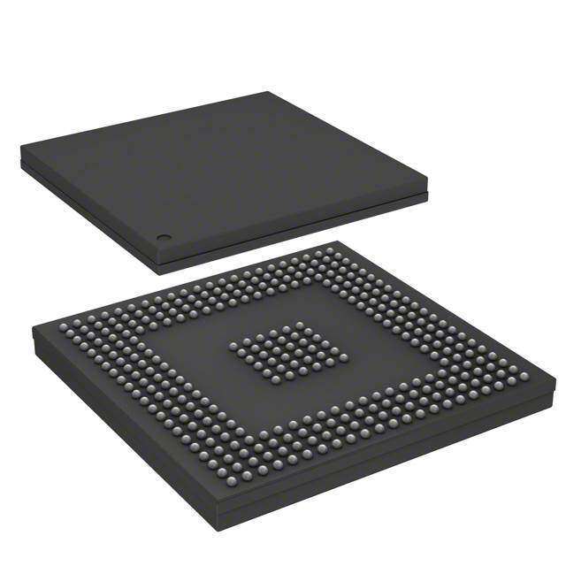
| 描述 | IC MCU 32BIT 4MB FLASH 516PBGA32位微控制器 - MCU 4M FLASH, 256K RAM z7, 264mhz |
| EEPROM容量 | - |
| 产品分类 | |
| I/O数 | 32 |
| 品牌 | Freescale Semiconductor |
| 产品手册 | |
| 产品图片 |
|
| rohs | 符合RoHS无铅 / 符合限制有害物质指令(RoHS)规范要求 |
| 产品系列 | 嵌入式处理器和控制器,微控制器 - MCU,32位微控制器 - MCU,Freescale Semiconductor SPC5674FF3MVY3MPC56xx Qorivva |
| 数据手册 | |
| 产品型号 | SPC5674FF3MVY3 |
| PCN组件/产地 | http://cache.freescale.com/files/shared/doc/pcn/PCN16151.htm |
| PCN设计/规格 | http://cache.freescale.com/files/shared/doc/pcn/PCN15860.htm?fsrch=1&WT_TYPE=Product |
| RAM容量 | 256K x 8 |
| 产品种类 | 32位微控制器 - MCU |
| 供应商器件封装 | 516-PBGA (27x27) |
| 包装 | 托盘 |
| 单位重量 | 4.374 g |
| 商标 | Freescale Semiconductor |
| 处理器系列 | MPC5674F |
| 外设 | DMA,POR,PWM |
| 安装风格 | SMD/SMT |
| 封装 | Tray |
| 封装/外壳 | 516-BBGA |
| 封装/箱体 | PBGA-516 |
| 工作温度 | -40°C ~ 125°C |
| 工作电源电压 | 4.5 V to 5.5 V |
| 工厂包装数量 | 200 |
| 振荡器类型 | 外部 |
| 数据RAM大小 | 16 kB |
| 数据总线宽度 | 32 bit |
| 数据转换器 | A/D 64x12b |
| 最大工作温度 | + 125 C |
| 最大时钟频率 | 264 MHz |
| 最小工作温度 | - 40 C |
| 标准包装 | 200 |
| 核心 | e200z7 |
| 核心处理器 | e200z7 |
| 核心尺寸 | 32-位 |
| 片上ADC | Yes |
| 电压-电源(Vcc/Vdd) | 1.08 V ~ 1.32 V |
| 程序存储器大小 | 4 MB |
| 程序存储器类型 | 闪存 |
| 程序存储容量 | 4MB(4M x 8) |
| 连接性 | CAN,EBI/EMI,SCI,SPI |
| 速度 | 264MHz |


- 商务部:美国ITC正式对集成电路等产品启动337调查
- 曝三星4nm工艺存在良率问题 高通将骁龙8 Gen1或转产台积电
- 太阳诱电将投资9.5亿元在常州建新厂生产MLCC 预计2023年完工
- 英特尔发布欧洲新工厂建设计划 深化IDM 2.0 战略
- 台积电先进制程称霸业界 有大客户加持明年业绩稳了
- 达到5530亿美元!SIA预计今年全球半导体销售额将创下新高
- 英特尔拟将自动驾驶子公司Mobileye上市 估值或超500亿美元
- 三星加码芯片和SET,合并消费电子和移动部门,撤换高东真等 CEO
- 三星电子宣布重大人事变动 还合并消费电子和移动部门
- 海关总署:前11个月进口集成电路产品价值2.52万亿元 增长14.8%


PDF Datasheet 数据手册内容提取
Freescale Semiconductor Document Number: MPC5674F Data Sheet: Advance Information Rev. 10.1, 06/2015 MPC5674F MPC5674F Microcontroller TEPBGA–416 TEPBGA–516 27mmx27mm 27mmx27mm Data Sheet Covers: MPC5674F and MPC5673F TEPBGA–324 23mmx23mm • Dual issue, 32-bit CPU core complex (e200z7) single action, double action, pulse width modulation – Compliant with the Power Architecture® embedded (PWM) and modulus counter operation category • Four enhanced queued analog-to-digital converters – 16KB I-Cache and 16KB D-Cache (eQADC) – Includes an instruction set enhancement allowing – Support for 64 analog channels variable length encoding (VLE), optional encoding of – Includes one absolute reference ADC channel mixed 16-bit and 32-bit instructions, for code size – Includes eight decimation filters footprint reduction • Four deserial serial peripheral interface (DSPI) modules – Includes signal processing extension (SPE2) instruction • Three enhanced serial communication interface (eSCI) support for digital signal processing (DSP) and modules single-precision floating point operations • Four controller area network (FlexCAN) modules • 4MB on-chip flash • Dual-channel FlexRay controller – Supports read during program and erase operations, and • Nexus development interface (NDI) per IEEE-ISTO multiple blocks allowing EEPROM emulation 5001-2003/5001-2008 standard • 256KB on-chip general-purpose SRAM including 32KB • Device and board test support per Joint Test Action Group of standby RAM (JTAG) (IEEE 1149.1) • Two direct memory access controller (eDMA2) blocks • On-chip voltage regulator controller regulates supply – One supporting 64 channels voltage down to 1.2V for core logic – One supporting 32 channels • Interrupt controller (INTC) • Frequency modulated phase-locked loop (FMPLL) • Crossbar switch architecture for concurrent access to peripherals, flash, or RAM from multiple bus masters • External bus interface (EBI) for calibration and application development (not available on all packages) • System integration unit (SIU) • Error correction status module (ECSM) • Boot assist module (BAM) supports serial bootload via CAN or SCI • Two second-generation enhanced time processor units (eTPU2) that share code and data RAM. – 32 standard channels per eTPU2 – 24KB code RAM – 6KB parameter (data) RAM • Enhanced modular input output system supporting 32 unified channels (eMIOS) with each channel capable of ©Freescale Semiconductor, Inc., 2008-2015. All rights reserved.
Table of Contents 1 Ordering Information. . . . . . . . . . . . . . . . . . . . . . . . . . . . . . . . .3 4.7.3 LVDS Pad Specifications . . . . . . . . . . . . . . . . . 35 1.1 Orderable Parts. . . . . . . . . . . . . . . . . . . . . . . . . . . . . . . .3 4.8 Oscillator and FMPLL Electrical Characteristics . . . . . 35 1.2 MPC567xF Family Differences. . . . . . . . . . . . . . . . . . . .4 4.9 eQADC Electrical Characteristics . . . . . . . . . . . . . . . . 37 2 MPC5674F Blocks . . . . . . . . . . . . . . . . . . . . . . . . . . . . . . . . . .5 4.9.1 ADC Internal Resource Measurements . . . . . . 39 2.1 Block Diagram. . . . . . . . . . . . . . . . . . . . . . . . . . . . . . . . .5 4.10 C90 Flash Memory Electrical Characteristics . . . . . . . 40 3 Pin Assignments. . . . . . . . . . . . . . . . . . . . . . . . . . . . . . . . . . . .5 4.11 AC Specifications. . . . . . . . . . . . . . . . . . . . . . . . . . . . . 42 3.1 324-ball TEPBGA Pin Assignments . . . . . . . . . . . . . . . .6 4.11.1 Clocking. . . . . . . . . . . . . . . . . . . . . . . . . . . . . . 42 3.2 416-ball TEPBGA Pin Assignments . . . . . . . . . . . . . . . .9 4.11.2 Pad AC Specifications . . . . . . . . . . . . . . . . . . . 44 3.3 516-ball TEPBGA Pin Assignments . . . . . . . . . . . . . . .14 4.12 AC Timing . . . . . . . . . . . . . . . . . . . . . . . . . . . . . . . . . . 45 3.4 Signal Properties and Muxing. . . . . . . . . . . . . . . . . . . .19 4.12.1 Generic Timing Diagrams. . . . . . . . . . . . . . . . . 45 4 Electrical Characteristics . . . . . . . . . . . . . . . . . . . . . . . . . . . .20 4.12.2 Reset and Configuration Pin Timing. . . . . . . . . 46 4.1 Maximum Ratings. . . . . . . . . . . . . . . . . . . . . . . . . . . . .20 4.12.3 IEEE 1149.1 Interface Timing. . . . . . . . . . . . . . 47 4.2 Thermal Characteristics . . . . . . . . . . . . . . . . . . . . . . . .21 4.12.4 Nexus Timing. . . . . . . . . . . . . . . . . . . . . . . . . . 50 4.2.1 General Notes for Specifications at 4.12.5 External Bus Interface (EBI) Timing. . . . . . . . . 53 Maximum Junction Temperature . . . . . . . . . . . .23 4.12.6 External Interrupt Timing (IRQ Pin) . . . . . . . . . 57 4.3 EMI (Electromagnetic Interference) Characteristics. . .24 4.12.7 eTPU Timing . . . . . . . . . . . . . . . . . . . . . . . . . . 57 4.4 ESD Characteristics . . . . . . . . . . . . . . . . . . . . . . . . . . .25 4.12.8 eMIOS Timing . . . . . . . . . . . . . . . . . . . . . . . . . 58 4.5 PMC/POR/LVI Electrical Specifications . . . . . . . . . . . .25 4.12.9 DSPI Timing. . . . . . . . . . . . . . . . . . . . . . . . . . . 59 4.6 Power Up/Down Sequencing . . . . . . . . . . . . . . . . . . . .29 5 Package Information. . . . . . . . . . . . . . . . . . . . . . . . . . . . . . . 65 4.6.1 Power-Up. . . . . . . . . . . . . . . . . . . . . . . . . . . . . .29 5.1 324-Pin Package. . . . . . . . . . . . . . . . . . . . . . . . . . . . . 66 4.6.2 Power-Down . . . . . . . . . . . . . . . . . . . . . . . . . . .30 5.2 416-Pin Package. . . . . . . . . . . . . . . . . . . . . . . . . . . . . 68 4.6.3 Power Sequencing and POR Dependent on V 5.3 516-Pin Package. . . . . . . . . . . . . . . . . . . . . . . . . . . . . 70 DDA 30 6 Product Documentation. . . . . . . . . . . . . . . . . . . . . . . . . . . . . 72 4.7 DC Electrical Specifications . . . . . . . . . . . . . . . . . . . . .30 AppendixASignal Properties and Muxing. . . . . . . . . . . . . . . . . . 73 4.7.1 I/O Pad Current Specifications . . . . . . . . . . . . .33 AppendixBRevision History . . . . . . . . . . . . . . . . . . . . . . . . . . . 125 4.7.2 I/O Pad V Current Specifications . . . . . . . .34 DD33 MPC5674F Microcontroller Data Sheet, Rev. 10.1 2 Freescale Semiconductor
Ordering Information 1 Ordering Information 1.1 Orderable Parts Figure1 and Table1 describe and list the orderable part numbers for the MPC5674F. M PC5674F F 3 MVR 3 R Qualification status Core code Note:Not all options are available on all Device number devices. Refer to Fab Revision ID Table1. Revision of Silicon Temperature range Package identifier Operating frequency (MHz) Tape and reel status Temperature Range Package Identifier Operating Frequency Tape and Reel Status M=–40 °C to 125 °C VZ=324 BGA Pb-free 2=200MHz R=Tape and reel VR=416 BGA Pb-free 3=264MHz (blank)=Trays VY=516 BGA Pb-free VV=516 BGA SnPb Qualification Status Revision of Silicon Fab Revision ID P=Pre qualification 3=Rev 3 (ATMC) F=ATMC M=Fully spec. qualified, general market flow 0 = Rev 0 (TSMC14) K = TSMC14 S=Fully spec. qualified, automotive flow Figure1. MPC5674F Orderable Part Number Description Table1. Orderable Part Numbers Speed (MHz)1 Operating Temperature2 Freescale Part Number Package Description Nominal Max3 (f ) Min (T ) Max (T ) MAX L H SPC5674FK0MVR3 416 PBGA, no EBI, Pb-free 264 270 –40 °C 125 °C SPC5674FK0MVY3 516 PBGA, w/EBI, Pb-free 264 270 –40 °C 125 °C SPC5674FK0MVV3R 516 PBGA, w/EBI, SnPb 264 270 –40 °C 125 °C SPC5674FK0MVV3 516 PBGA, w/EBI, SnPb 264 200 –40 °C 125 °C SPC5674FK0MVY3R 516 PBGA, w/EBI, Pb-free 264 270 –40 °C 125 °C SPC5674FK0MVY3 516 PBGA, w/EBI, Pb-free 264 270 –40 °C 125 °C SPC5673FK0MVR2R 416 PBGA, no EBI, Pb-free 200 200 –40 °C 125 °C SPC5673FK0MVR2 416 PBGA, no EBI, Pb-free 200 200 –40 °C 125 °C SPC5673FK0MVV2R 324 PBGA, no EBI, Pb-free 200 200 –40 °C 125 °C SPC5673FK0MVV2 324 PBGA, no EBI, Pb-free 200 200 –40 °C 125 °C 1 For the operating mode frequency of various blocks on the device, see Table28. MPC5674F Microcontroller Data Sheet, Rev. 10.1 Freescale Semiconductor 3
Ordering Information 2 The lowest ambient operating temperature is referenced by T ; the highest ambient operating temperature is referenced by T . L H 3 Speed is the nominal maximum frequency. Max speed is the maximum speed allowed including frequency modulation (FM). 270MHz parts allow for 264MHz system clock + 2% FM. 1.2 MPC567xF Family Differences Table2 lists the differences between the MPC567xF devices. Refer to the MPC5674F Reference Manual for a full feature list and comparison. Table2. MPC567xF Family Differences Feature MPC5674F MPC5674F MPC5673F MPC5673F Package 416 BGA 324 BGA 416 BGA 324 BGA 516 BGA 516 BGA Flash 4 MB 4 MB 3 MB 3 MB SRAM 256 KB 256 KB 192 KB 192 KB External bus Yes No Yes No (516 BGA only) (516 BGA only) Serial 3 2 3 2 eSCI_A Yes Yes Yes Yes eSCI_B Yes Yes Yes Yes eSCI_C Yes No Yes No SPI 4 3 4 3 DSPI_A Yes No Yes No DSPI_B Yes Yes Yes Yes DSPI_C Yes Yes Yes Yes DSPI_D Yes Yes Yes Yes eMIOS 32 channel 22 channel 32 channel 22 channel eTPU2 64 channel 47 channel 64 channel 47 channel eTPU_A Yes (32 ch) Yes (26 ch) Yes Yes (26 ch) eTPU_B Yes (32 ch) Yes (21 ch, no Yes Yes (21 ch, no TCRCLK) TCRCLK) ADC 64 channel 48 channel 64 channel 48 channel eQADC_A Yes (24 ch) Yes (24 ch) Yes (64 ch)1 Yes (64 ch)1 eQADC_B Yes (24 ch) Yes (24 ch) 1 There are are two pairs of 24 channels plus 16 shared channels. This gives 64 channels total: 40 per ADC (since 16 are shared). MPC5674F Microcontroller Data Sheet, Rev. 10.1 4 Freescale Semiconductor
MPC5674F Blocks 2 MPC5674F Blocks 2.1 Block Diagram Figure2 shows a top-level block diagram of the MPC5674F device. MPC5674F Power™ e200z7 Core SPE2 Interrupt Nexus Controller VLE JTAG MMU eDMA2 eDMA2 16K 16K 64 Channel 32 Channel I-Cache D-Cache FlexRay EBI (Calibration & Crossbar Switch Development Use) MPU 4MB I/O 256KB SRAM Boot Assist I/O SIU ECSM Flash Bridge (32K S/B) Module Bridge 6KB N N N N x8 eQADC eQADC eM3I2OS eT3P2U2 RDAatMa eT3P2U2 eSCI eSCI eSCI DSPI DSPI DSPI DSPI FlexCA FlexCA FlexCA FlexCA DECFIL CADCCi CADCCi Channel Channel 24KB Channel D D D D Code A A A A RAM AMux LEGEND ADC – Analog to digital convertor eSCI – Enhanced serial communications interface ADCi – ADC interface eTPU2 – Enhanced time processing unit 2 AMux – Analog multiplexer FlexCAN– Controller area network DECFIL – Decimation filter MMU – Memory management unit DSPI – Deserial/serial peripheral interface MPU – Memory protection unit EBI – External bus interface S/B – Stand-by ECSM – Error correction status module SIU – System integration unit eDMA2 – Enhanced direct memory access SPE2 – Signal processing engine 2 eMIOS – Enhanced modular I/O system SRAM – General-purpose static RAM eQADC – Enhanced queued A/D converter module VLE – Variable length instruction encoding Figure2. Block Diagram 3 Pin Assignments The figures in this section show the primary pin function. For the full signal properties and muxing table, see AppendixA, Signal Properties and Muxing. MPC5674F Microcontroller Data Sheet, Rev. 10.1 Freescale Semiconductor 5
Pin Assignments 3.1 324-ball TEPBGA Pin Assignments Figure3 shows the 324-ball TEPBGA pin assignments. The same information is shown in Figure4 through Figure5. 1 2 3 4 5 6 7 8 9 10 11 12 13 14 15 16 17 18 19 20 21 22 REF– REF– A VSS VDD RSTOUT ANA0 ANA1 ANA4 ANA5 ANA15 VDDA_A0 VRH_A VRL_A VDDA_ B0 VRL_B VRH_B ANB2 ANB3 ANB6 ANB7 ANB22 VSS A BYPCB1 BYPCB1 REF– REF– B VDDEH1 VSS VDD TEST ANA2 ANA3 ANA6 ANA7 VDDA_A0VSSA_A1 BYPCA BYPCBVDDA_ B1VSSA_ B0 ANB0 ANB1 ANB4 ANB5 ANB19 ANB23 VSS TCRCLKCB C ETPUA21ETPUA26 VSS VDD ANA8 ANA10 ANA9 ANA13 ANA17 ANA19 ANA21 ANA23 ANB10 ANB9 ANB11 ANB12 ANB14 ANB16 ANB20 VSS ETPUC0 VDDEH7 C D ETPUA23ETPUA25ETPUA31 VSS VDD ANA11 ANA12 ANA14 ANA16 ANA18 ANA20 ANA22 ANB8 ANB13 ANB15 ANB17 ANB18 ANB21 VSS ETPUC1 ETPUC3 ETPUC2 D E ETPUA20ETPUA22ETPUA24ETPUA30 ETPUC5ETPUC10ETPUC11 ETPUC4 E F ETPUA13ETPUA14ETPUA15ETPUA27 MPC5674F 324 TEPBGA ETPUC12ETPUC14ETPUC13ETPUC9 F (as viewed from top through the package) G ETPUA10ETPUA11ETPUA12ETPUA17 ETPUC20ETPUC18ETPUC19ETPUC17G H ETPUA5 ETPUA6 ETPUA9ETPUA16 VDDEH7ETPUC23ETPUC22ETPUC21H J ETPUA1 ETPUA2 ETPUA3 ETPUA4 VSS VSS VSS VSS VSS VSS ETPUC27ETPUC28ETPUC26ETPUC24J KTCRCLKAETPUA0 VDD VSTBY VSS VSS VSS VSS VSS VSS ETPUC31ETPUC30ETPUC29ETPUC25K BOOT- L PLLCFG1PLLCFG2VDDEH1 VSS VSS VSS VSS VSS VSS ETPUB12ETPUB13ETPUB14VDDEH7 L CFG1 M JCOMP RESET PLLCFG0 RDY VDDE2 VSS VSS VSS VSS VSS ETPUB7ETPUB10ETPUB11ETPUB9 M N VDDE2 MCKO MSEO1 EVTI VDDE2 VDDE2 VSS VSS VSS VSS ETPUB0 VDDEH6 ETPUB8 ETPUB6 N P EVTO MSEO0 MDO0 MDO1 VDDE2 VDDE2 VSS VSS VSS VSS TCRCLKBETPUB16ETPUB5 ETPUB4 P R MDO2 MDO3 MDO4 MDO5 ETPUB1ETPUB17ETPUB3 ETPUB2 R T MDO6 MDO7 MDO8 VDDE2 ETPUB19ETPUB18VDDEH6REGCTL T U MDO9 MDO10 MDO11 MDO15 ETPUB31ETPUB30VDDREGVSSSYN U V MDO12 VDDE2 MDO14 VDD33_2 VDD REGSEL VSSFL EXTAL V W TDO MDO13 TMS VSS VDD VDDE2 PCSB2 VDDEH4 VDD EMIOS8 EMIOS9 EMIOS18EMIOS22EMIOS27EMIOS31 CNTXC CNRXC CNRXB VSS VDD VDD33_3 XTAL W FR_A_ FR_B_ Y TCK TDI VSS VDD SCKA SCKB PCSB0 EMIOS2 EMIOS5EMIOS14EMIOS15EMIOS19EMIOS23EMIOS26EMIOS30 CNTXB CNRXD VSS VDD VDDSYN Y TX TX FR_A_ FR_B_ AA ENGCLK VSS VDD PCSA5 SINA SINB EMIOS0 EMIOS3EMIOS10EMIOS13EMIOS17EMIOS21EMIOS25EMIOS28EMIOS29 CNRXA SCKC SINC VSS VDD AA RX RX FR_A_ FR_B_ AB VSS VDD TX_EN VDDE2 TX_EN PCSA0 SOUTA SOUTB EMIOS1 EMIOS4 EMIOS7EMIOS11EMIOS12EMIOS16EMIOS20EMIOS24 CNTXA SOUTC PCSC0 VDDEH4 CNTXD VSS AB 1 2 3 4 5 6 7 8 9 10 11 12 13 14 15 16 17 18 19 20 21 22 Figure3. MPC5674F 324-ball TEPBGA (full diagram) MPC5674F Microcontroller Data Sheet, Rev. 10.1 6 Freescale Semiconductor
Pin Assignments 1 2 3 4 5 6 7 8 9 10 11 A VSS VDD RSTOUT ANA0 ANA1 ANA4 ANA5 ANA15 VDDA_A0 VRH_A VRL_A A REF– B VDDEH1 VSS VDD TEST ANA2 ANA3 ANA6 ANA7 VDDA_A0VSSA_A1 B BYPCA C ETPUA21ETPUA26 VSS VDD ANA8 ANA10 ANA9 ANA13 ANA17 ANA19 ANA21 C D ETPUA23ETPUA25ETPUA31 VSS VDD ANA11 ANA12 ANA14 ANA16 ANA18 ANA20 D E ETPUA20ETPUA22ETPUA24ETPUA30 F ETPUA13ETPUA14ETPUA15ETPUA27 MPC5674F 324 TEPBGA (as viewed from top through the package) G ETPUA10ETPUA11ETPUA12ETPUA17 H ETPUA5 ETPUA6 ETPUA9 ETPUA16 J ETPUA1 ETPUA2 ETPUA3 ETPUA4 VSS VSS VSS J KTCRCLKA ETPUA0 VDD VSTBY VSS VSS VSS K BOOT- L PLLCFG1PLLCFG2 VDDEH1 VSS VSS VSS L CFG1 M JCOMP RESET PLLCFG0 RDY VDDE2 VSS VSS M N VDDE2 MCKO MSEO1 EVTI VDDE2 VDDE2 VSS N P EVTO MSEO0 MDO0 MDO1 VDDE2 VDDE2 VSS P R MDO2 MDO3 MDO4 MDO5 T MDO6 MDO7 MDO8 VDDE2 U MDO9 MDO10 MDO11 MDO15 V MDO12 VDDE2 MDO14 VDD33_2 W TDO MDO13 TMS VSS VDD VDDE2 PCSB2 VDDEH4 VDD EMIOS8 EMIOS9 W FR_A_ FR_B_ Y TCK TDI VSS VDD SCKA SCKB PCSB0 EMIOS2 EMIOS5 Y TX TX FR_A_ FR_B_ AA ENGCLK VSS VDD PCSA5 SINA SINB EMIOS0 EMIOS3 EMIOS10 AA RX RX FR_A_ FR_B_ AB VSS VDD TX_EN VDDE2 TX_EN PCSA0 SOUTA SOUTB EMIOS1 EMIOS4 EMIOS7 AB 1 2 3 4 5 6 7 8 9 10 11 Figure4. MPC5674F 324-ball TEPBGA (1 of 2) MPC5674F Microcontroller Data Sheet, Rev. 10.1 Freescale Semiconductor 7
Pin Assignments 12 13 14 15 16 17 18 19 20 21 22 REF– REF– A VDDA_ B0 VRL_B VRH_B ANB2 ANB3 ANB6 ANB7 ANB22 VSS A BYPCB1 BYPCB1 REF– B BYPCB VDDA_ B1VSSA_ B0 ANB0 ANB1 ANB4 ANB5 ANB19 ANB23 VSS TCRCLKCB C ANA23 ANB10 ANB9 ANB11 ANB12 ANB14 ANB16 ANB20 VSS ETPUC0 VDDEH7 C D ANA22 ANB8 ANB13 ANB15 ANB17 ANB18 ANB21 VSS ETPUC1 ETPUC3 ETPUC2 D ETPUC5 ETPUC10ETPUC11 ETPUC4 E MPC5674F 324 TEPBGA ETPUC12ETPUC14ETPUC13 ETPUC9 F (as viewed from top through the package) ETPUC20ETPUC18ETPUC19ETPUC17 G VDDEH7 ETPUC23ETPUC22ETPUC21 H J VSS VSS VSS ETPUC27ETPUC28ETPUC26ETPUC24J K VSS VSS VSS ETPUC31ETPUC30ETPUC29ETPUC25K L VSS VSS VSS ETPUB12ETPUB13ETPUB14 VDDEH7 L M VSS VSS VSS ETPUB7 ETPUB10ETPUB11 ETPUB9 M N VSS VSS VSS ETPUB0 VDDEH6 ETPUB8 ETPUB6 N P VSS VSS VSS TCRCLKBETPUB16 ETPUB5 ETPUB4 P ETPUB1 ETPUB17 ETPUB3 ETPUB2 R ETPUB19ETPUB18 VDDEH6 REGCTL T ETPUB31ETPUB30VDDREG VSSSYN U VDD REGSEL VSSFL EXTAL V W EMIOS18EMIOS22EMIOS27EMIOS31 CNTXC CNRXC CNRXB VSS VDD VDD33_3 XTAL W Y EMIOS14EMIOS15EMIOS19EMIOS23EMIOS26EMIOS30 CNTXB CNRXD VSS VDD VDDSYN Y AA EMIOS13EMIOS17EMIOS21EMIOS25EMIOS28EMIOS29 CNRXA SCKC SINC VSS VDD AA AB EMIOS11 EMIOS12EMIOS16EMIOS20EMIOS24 CNTXA SOUTC PCSC0 VDDEH4 CNTXD VSS AB 12 13 14 15 16 17 18 19 20 21 22 Figure5. MPC5674F 324-ball TEPBGA (2 of 2) MPC5674F Microcontroller Data Sheet, Rev. 10.1 8 Freescale Semiconductor
Pin Assignments 3.2 416-ball TEPBGA Pin Assignments Figure6 shows the 416-ball TEPBGA pin assignments in one figure. The same information is shown in Figure7 through Figure10. 1 2 3 4 5 6 7 8 9 10 11 12 13 14 15 16 17 18 19 20 21 22 23 24 25 26 REF– REF– A VSS VDD RSTOUT ANA0 ANA4 ANA8 ANA11 ANA15 VDDA_A0 VRL_A VRH_A AN28 AN32 AN36 VDDA_B0 VRL_B VRH_B ANB7 ANB11 ANB14 ANB17 ANB21 ANB23 VSS A BYPCA1 BYPCB1 REF– REF– B VDDEH1 VSS VDD TEST ANA1 ANA5 ANA10 ANA14 VDDA_A1VSSA_A1 AN24 AN27 AN29 AN33 VDDA_B1VSSA_B0 ANB6 ANB8 ANB10 ANB15 ANB18 ANB22 VSS TCRCLKCB BYPCA BYPCB CETPUA30ETPUA31 VSS VDD ANA2 ANA6 ANA9 ANA13 ANA17 ANA19 ANA21 ANA23 AN26 AN30 AN34 AN37 AN38 ANB0 ANB4 ANB5 ANB12 ANB16 ANB19 VSS ETPUC0 ETPUC1 C DETPUA27ETPUA28ETPUA29 VSS VDD ANA3 ANA7 ANA12 ANA16 ANA18 ANA20 ANA22 AN25 AN31 AN35 AN39 ANB1 ANB2 ANB3 ANB9 ANB13 ANB20 VSS VDDEH7ETPUC2 ETPUC3 D EETPUA23ETPUA24ETPUA25ETPUA26 VDDEH7ETPUC4 ETPUC5 ETPUC6 E FETPUA19ETPUA20ETPUA21ETPUA22 ETPUC7 ETPUC8 ETPUC9ETPUC10F MPC5674F 416-ball TEPBGA GETPUA15ETPUA16ETPUA17ETPUA18 ETPUC11ETPUC12ETPUC13ETPUC14G (as viewed from top through the package) HETPUA11ETPUA12ETPUA14ETPUA13 ETPUC15ETPUC16ETPUC17ETPUC18H J ETPUA7 ETPUA8 ETPUA9ETPUA10 ETPUC19ETPUC20ETPUC21ETPUC22J K ETPUA3ETPUA4ETPUA5ETPUA6 VSS VSS VSS VSS VSS VSS VSS VSS ETPUC23ETPUC24ETPUC25ETPUC26K LTCRCLKAETPUA0ETPUA1ETPUA2 VSS VSS VSS VSS VSS VSS VSS VSS ETPUC27ETPUC28ETPUC29ETPUC30L MVDD33_1 TXDA RXDA VSTBY VSS VSS VSS VSS VSS VSS VSS VSS ETPUC31ETPUB15ETPUB14VDDEH7 M BOOT– N RXDB WKPCFG VDD VDDE2 VSS VSS VSS VSS VSS VSS VSS VDDEH6ETPUB11ETPUB12ETPUB13N CFG1 P TXDB PLLCFG1PLLCFG2VDDEH1 VDDE2 VDDE2 VSS VSS VSS VSS VSS VSS ETPUB7 ETPUB8ETPUB9ETPUB10P R JCOMP RESET PLLCFG0 RDY VDDE2 VDDE2 VSS VSS VSS VSS VSS VSS ETPUB3 ETPUB4 ETPUB5ETPUB6 R T VDDE2 MCKO MSEO1 EVTI VDDE2 VDDE2 VDDE2 VSS VSS VSS VSS VSS TCRCLKBETPUB0 ETPUB1 ETPUB2 T U EVTO MSEO0 MDO0 MDO1 VDDE2 VDDE2 VDDE2 VSS VSS VSS VSS VSS ETPUB19ETPUB18ETPUB17ETPUB16U V MDO2 MDO3 MDO4 MDO5 ETPUB26ETPUB22ETPUB21ETPUB20V W MDO6 MDO7 MDO8 VDDE2 REGSELETPUB25ETPUB24ETPUB23W Y MDO9 MDO10 MDO11 MDO15 ETPUB29ETPUB28ETPUB27REGCTL Y AA MDO12 MDO13 MDO14VDD33_2 VDD33_3ETPUB30VDDREGVSSSYN AA AB TDO TCK TMS VDD VDD ETPUB31 VSSFL EXTAL AB AC VDDE2 TDI VDD VSS VDDE2 PCSA1 PCSA2 PCSB4 PCSB1 VDDEH3VDDEH4 VDD EMIOS8EMIOS14EMIOS18EMIOS22EMIOS27EMIOS31CNRXB CNRXD VDDEH5 PCSC1 VSS VDD VDDEH6 XTAL AC FR_A_ FR_B_ ADENGCLK VDD VSS PCSA5 SOUTA SCKA PCSB0 PCSB3 EMIOS2 EMIOS5 EMIOS9EMIOS15EMIOS19EMIOS23EMIOS26EMIOS30 CNTXB CNTXD SCKC RXDC PCSC3 VSS VDD VDDSYNAD TX TX FR_A_ FR_B_ AE VDD VSS PCSA4 PCSA0 PCSA3 SCKB SINB EMIOS0 EMIOS3 EMIOS6EMIOS10EMIOS13EMIOS17EMIOS21EMIOS25EMIOS29CNRXA CNRXC PCSC0 SINC PCSC2 PCSC5 VSS VDD AE RX RX FR_A_ FR_B_ AF VSS VDDE2 VDDEH3 PCSB5 SINA PCSB2 SOUTB EMIOS1 EMIOS4 EMIOS7EMIOS11EMIOS12EMIOS16EMIOS20EMIOS24EMIOS28 CNTXA CNTXC SOUTC VDDEH4 TXDC PCSC4 VDDEH5 VSS AF TX_EN TX_EN 1 2 3 4 5 6 7 8 9 10 11 12 13 14 15 16 17 18 19 20 21 22 23 24 25 26 Figure6. MPC5674F 416-ball TEPBGA (full diagram) MPC5674F Microcontroller Data Sheet, Rev. 10.1 Freescale Semiconductor 9
Pin Assignments 1 2 3 4 5 6 7 8 9 10 11 12 13 REFBYP- A VSS VDD RSTOUT ANA0 ANA4 ANA8 ANA11 ANA15 VDDA_A0 VRL_A VRH_A AN28 A CA1 B VDDEH1 VSS VDD TEST ANA1 ANA5 ANA10 ANA14 VDDA_A1VSSA_A1REFBYPCA AN24 AN27 B C ETPUA30 ETPUA31 VSS VDD ANA2 ANA6 ANA9 ANA13 ANA17 ANA19 ANA21 ANA23 AN26 C D ETPUA27 ETPUA28 ETPUA29 VSS VDD ANA3 ANA7 ANA12 ANA16 ANA18 ANA20 ANA22 AN25 D E ETPUA23 ETPUA24 ETPUA25 ETPUA26 E F ETPUA19 ETPUA20 ETPUA21 ETPUA22 F MPC5674F 416-ball TEPBGA G ETPUA15 ETPUA16 ETPUA17 ETPUA18 (as viewed from top through the package) G (1 of 4) H ETPUA11 ETPUA12 ETPUA14 ETPUA13 H J ETPUA7 ETPUA8 ETPUA9 ETPUA10 J K ETPUA3 ETPUA4 ETPUA5 ETPUA6 VSS VSS VSS VSS K L TCRCLKA ETPUA0 ETPUA1 ETPUA2 VSS VSS VSS VSS L M VDD33_1 TXDA RXDA VSTBY VSS VSS VSS VSS M N RXDB BOOTCFG1WKPCFG VDD VDDE2 VSS VSS VSS N 1 2 3 4 5 6 7 8 9 10 11 12 13 Figure7. MPC5674F 416-ball TEPBGA (1 of 4) MPC5674F Microcontroller Data Sheet, Rev. 10.1 10 Freescale Semiconductor
Pin Assignments 14 15 16 17 18 19 20 21 22 23 24 25 26 REFBYP- A AN32 AN36 VDDA_B0 VRL_B VRH_B ANB7 ANB11 ANB14 ANB17 ANB21 ANB23 VSS A CB1 B AN29 AN33 VDDA_B1VSSA_B0REFBYPCB ANB6 ANB8 ANB10 ANB15 ANB18 ANB22 VSS TCRCLKC B C AN30 AN34 AN37 AN38 ANB0 ANB4 ANB5 ANB12 ANB16 ANB19 VSS ETPUC0 ETPUC1 C D AN31 AN35 AN39 ANB1 ANB2 ANB3 ANB9 ANB13 ANB20 VSS VDDEH7 ETPUC2 ETPUC3 D E VDDEH7 ETPUC4 ETPUC5 ETPUC6 E F ETPUC7 ETPUC8 ETPUC9 ETPUC10 F MPC5674F 416-ball TEPBGA G (as viewed from top through the package) ETPUC11 ETPUC12 ETPUC13 ETPUC14 G (2 of 4) H ETPUC15 ETPUC16 ETPUC17 ETPUC18 H J ETPUC19 ETPUC20 ETPUC21 ETPUC22 J K VSS VSS VSS VSS ETPUC23 ETPUC24 ETPUC25 ETPUC26 K L VSS VSS VSS VSS ETPUC27 ETPUC28 ETPUC29 ETPUC30 L M VSS VSS VSS VSS ETPUC31 ETPUB15 ETPUB14 VDDEH7 M N VSS VSS VSS VSS VDDEH6 ETPUB11 ETPUB12 ETPUB13 N 14 15 16 17 18 19 20 21 22 23 24 25 26 Figure8. MPC5674F 416-ball TEPBGA (2 of 4) MPC5674F Microcontroller Data Sheet, Rev. 10.1 Freescale Semiconductor 11
Pin Assignments 1 2 3 4 5 6 7 8 9 10 11 12 13 P TXDB PLLCFG1 PLLCFG2 VDDEH1 VDDE2 VDDE2 VSS VSS P R JCOMP RESET PLLCFG0 RDY VDDE2 VDDE2 VSS VSS R T VDDE2 MCKO MSEO1 EVTI VDDE2 VDDE2 VDDE2 VSS T U EVTO MSEO0 MDO0 MDO1 U VDDE2 VDDE2 VDDE2 VSS V MDO2 MDO3 MDO4 MDO5 V W MDO6 MDO7 MDO8 VDDE2 W MPC5674F 416-ball TEPBGA Y MDO9 MDO10 MDO11 MDO15 (as viewed from top through the package) Y (3 of 4) AA MDO12 MDO13 MDO14 VDD33_2 AA AB TDO TCK TMS VDD AB AC VDDE2 TDI VDD VSS VDDE2 PCSA1 PCSA2 PCSB4 PCSB1 VDDEH3 VDDEH4 VDD EMIOS8 AC AD ENGCLK VDD VSS FR_A_TX FR_B_TX PCSA5 SOUTA SCKA PCSB0 PCSB3 EMIOS2 EMIOS5 EMIOS9 AD AE VDD VSS FR_A_RX FR_B_RX PCSA4 PCSA0 PCSA3 SCKB SINB EMIOS0 EMIOS3 EMIOS6 EMIOS10 AE FR_A_ FR_B_ AF VSS VDDE2 VDDEH3 PCSB5 SINA PCSB2 SOUTB EMIOS1 EMIOS4 EMIOS7 EMIOS11 AF TX_EN TX_EN 1 2 3 4 5 6 7 8 9 10 11 12 13 Figure9. MPC5674F 416-ball TEPBGA (3 of 4) MPC5674F Microcontroller Data Sheet, Rev. 10.1 12 Freescale Semiconductor
Pin Assignments 14 15 16 17 18 19 20 21 22 23 24 25 26 P VSS VSS VSS VSS ETPUB7 ETPUB8 ETPUB9 ETPUB10 P R VSS VSS VSS VSS ETPUB3 ETPUB4 ETPUB5 ETPUB6 R T VSS VSS VSS VSS TCRCLKB ETPUB0 ETPUB1 ETPUB2 T U VSS VSS VSS VSS ETPUB19 ETPUB18 ETPUB17 ETPUB16 U V ETPUB26 ETPUB22 ETPUB21 ETPUB20 V W REGSEL ETPUB25 ETPUB24 ETPUB23 W MPC5674F 416-ball TEPBGA Y (as viewed from top through the package) ETPUB29 ETPUB28 ETPUB27 REGCTL Y (4 of 4) AA VDD33_3 ETPUB30 VDDREG VSSSYN AA AB VDD ETPUB31 VSSFL EXTAL AB AC EMIOS14 EMIOS18 EMIOS22 EMIOS27 EMIOS31 CNRXB CNRXD VDDEH5 PCSC1 VSS VDD VDDEH6 XTAL AC AD EMIOS15 EMIOS19 EMIOS23 EMIOS26 EMIOS30 CNTXB CNTXD SCKC RXDC PCSC3 VSS VDD VDDSYN AD AE EMIOS13 EMIOS17 EMIOS21 EMIOS25 EMIOS29 CNRXA CNRXC PCSC0 SINC PCSC2 PCSC5 VSS VDD AE AF EMIOS12 EMIOS16 EMIOS20 EMIOS24 EMIOS28 CNTXA CNTXC SOUTC VDDEH4 TXDC PCSC4 VDDEH5 VSS AF 14 15 16 17 18 19 20 21 22 23 24 25 26 Figure10. MPC5674F 416-ball TEPBGA (4 of 4) MPC5674F Microcontroller Data Sheet, Rev. 10.1 Freescale Semiconductor 13
Pin Assignments 3.3 516-ball TEPBGA Pin Assignments Figure11 shows the 516-ball TEPBGA pin assignments in one figure. The same information is shown split into four quadrants in Figure12 through Figure15. 1 2 3 4 5 6 7 8 9 10 11 12 13 14 15 16 17 18 19 20 21 22 23 24 25 26 REF– REF– A VDD RSTOUT ANA0 ANA4 ANA9 ANA11 ANA15 VDDA_A0 VRL_A VRH_A AN28 AN29 AN36 VDDA_B0 VRL_B VRH_B ANB5 ANB9 ANB12 ANB18 ANB21 VSS A BYPCA1 BYPCB1 REF– REF– B VDDEH1 VSS VDD TEST ANA1 ANA5 ANA10 ANA14 VDDA_A1VSSA_A1 AN24 AN27 AN30 AN32 VDDA_B1VSSA_B0 ANB4 ANB8 ANB10 ANB13 ANB19 ANB22 VSS VSS B BYPCA BYPCB CETPUA30ETPUA31 VSS VDD ANA2 ANA6 ANA7 ANA13 ANA17 ANA19 ANA21 ANA22 AN25 AN31 AN34 AN39 AN37 ANB0 ANB7 ANB6 ANB11 ANB15 ANB20 VSS ETPUC0ETPUC1 C DETPUA27ETPUA28ETPUA29 VSS VDD ANA3 ANA8 ANA12 ANA16 ANA18 ANA20 ANA23 AN26 AN33 AN35 AN38 ANB1 ANB2 ANB3 ANB14 ANB16 ANB17 VSS VDDEH7ETPUC2ETPUC3 D EETPUA23ETPUA24ETPUA25ETPUA26 VSS VDD VSS VSS VSS VSS VSS VSS VSS VSS VSS VSS VSS VSS VSS ANB23 VSS VSS VDDEH7ETPUC4ETPUC5ETPUC6 E FETPUA19ETPUA20ETPUA21ETPUA22 VSS VDDE8 VDDE8 VDDE8 VDDE8 VSS VSS VDDE10VDDE10 VDDE10 VDDE10TCRCLKCETPUC7ETPUC8ETPUC9ETPUC10F GETPUA11ETPUA13ETPUA15ETPUA17ETPUA18 MPC5674F 516-ball TEPBGA ETPUC11ETPUC12ETPUC13ETPUC14ETPUC15G H ETPUA5ETPUA7ETPUA8ETPUA3ETPUA14ETPUA16 ETPUC19ETPUC16ETPUC17ETPUC18ETPUC20ETPUC21H (as viewed from top through the package) J ETPUA1ETPUA2ETPUA9ETPUA4ETPUA12 ETPUC22ETPUC23ETPUC24ETPUC26ETPUC27J K TXDB TXDA RXDA TCRCLKAETPUA6ETPUA10 VSS VSS VSS VSS VSS VSS VSS VSS ETPUC25ETPUC28ETPUC29ETPUC30ETPUC31D_DAT15K BOOT– BOOT– LPLLCFG1PLLCFG2 RXDB ETPUA0 VSS VSS VSS VSS VSS VSS VSS VSS VDD33_6D_DAT14D_DAT13D_DAT12D_DAT11D_DAT10L CFG1 CFG0 MVDD33_1D_BDIPPLLCFG0 VSTBY WKPCFG VSS VSS VSS VSS VSS VSS VSS VSS D_DAT9 D_DAT8 D_DAT7 D_DAT5VDDEH7 M N D_WE0 D_WE2 D_WE3 VDD RESET VDDE8 VDDE2 VSS VSS VSS VSS VSS VSS VSS VDDE10 D_DAT6VDDEH6 D_DAT2 D_DAT3 D_DAT4 N P D_ADD9D_ADD10D_ADD11VDDEH1 D_WE1VDD33_1 VDDE2 VDDE2 VSS VSS VSS VSS VSS VSS VDDE10ETPUB13 D_OE D_ALE D_DAT0 D_DAT1 P D_RD_ RD_ADD12D_ADD13D_ADD14D_ADD15D_ADD16 VDDE2 VDDE2 VSS VSS VSS VSS VSS VSS ETPUB9ETPUB12ETPUB14ETPUB15 R WR T VDDE2 D_ADD18D_ADD19D_ADD20D_ADD17 D_CS3 VDDE2 VDDE2 VDDE2 VSS VSS VSS VSS VSS ETPUB17ETPUB3ETPUB7ETPUB8ETPUB10ETPUB11T U D_CS2 JCOMP RDY MCKO MSEO1 MSEO0 VDDE2 VDDE2 VDDE2 VSS VSS VSS VSS VSS ETPUB23ETPUB1ETPUB2ETPUB4ETPUB5ETPUB6 U V EVTI EVTO MDO0 MDO2 MDO3 ETPUB21ETPUB22ETPUB16TCRCLKBETPUB0 V W MDO4 MDO5 MDO6 VDDE2 MDO8 MDO1 ETPUB25ETPUB29REGSELETPUB20ETPUB19ETPUB18W Y MDO7 MDO9 MDO10 MDO11 MDO12 ETPUB31ETPUB26ETPUB27ETPUB24REGCTL Y AA MDO13 MDO14 MDO15VDD33_1 VDDE8 VSS PCSA5 SOUTBVDD33_4 VDDE9 VDD33_4 EMIOS23EMIOS31 CNRXB VSS VDDE10VDD33_3ETPUB28VDDREGVSSSYN AA AB TDO TCK TMS VDD VSS VDDE9 VDDE9 SCKA SINB D_CS1 D_ADD21D_ADD29EMIOS1EMIOS11EMIOS17EMIOS19EMIOS29 VDDE9 VDDE9 VDDE9 VDDE9 VSS VDD ETPUB30 VSSFL EXTAL AB AC VDDE2 TDI VDD VSS VDDE2 PCSA1 SOUTA SCKB PCSB3 VDDEH3VDDEH4 VDD EMIOS0 EMIOS8EMIOS13EMIOS22EMIOS24EMIOS28 CNTXB CNRXD VDDEH5 PCSC1 VSS VDD VDDEH6 XTAL AC FR_A_ FR_B_ ADENGCLK VDD VSS PCSA0 PCSA3 PCSB2 D_CS0 D_ADD22D_ADD25D_ADD28EMIOS2 EMIOS7EMIOS12EMIOS16EMIOS18EMIOS27CNRXA CNTXD SCKC RXDC PCSC3 VSS VDD VDDSYNAD TX TX FR_A_ FR_B_ AE VDD VSS PCSA4 PCSB5 SINA PCSB1 D_TS D_ADD23D_ADD26D_ADD30EMIOS3 EMIOS6EMIOS10EMIOS15EMIOS21EMIOS26 CNTXA CNRXC PCSC0 SINC PCSC2 PCSC5 VSS VDD AE RX RX FR_A_ FR_B_ D_ AF VDDE2 TX_EN TX_EN VDDEH3 PCSA2 PCSB4 PCSB0 D_TA D_ADD24D_ADD27CLKOUTEMIOS4 EMIOS5 EMIOS9EMIOS20EMIOS14EMIOS25EMIOS30CNTXC SOUTC VDDEH4 TXDC PCSC4 VDDEH5 AF 1 2 3 4 5 6 7 8 9 10 11 12 13 14 15 16 17 18 19 20 21 22 23 24 25 26 Figure11. MPC5674F 516-ball TEPBGA (full diagram) MPC5674F Microcontroller Data Sheet, Rev. 10.1 14 Freescale Semiconductor
Pin Assignments 1 2 3 4 5 6 7 8 9 10 11 12 13 REF- A VDD RSTOUT ANA0 ANA4 ANA9 ANA11 ANA15 VDDA_A0 VRL_A VRH_A AN28 A BYPCA1 B VDDEH1 VSS VDD TEST ANA1 ANA5 ANA10 ANA14 VDDA_A1 VSSA_A1REFBYPCA AN24 AN27 B C ETPUA30 ETPUA31 VSS VDD ANA2 ANA6 ANA7 ANA13 ANA17 ANA19 ANA21 ANA22 AN25 C D ETPUA27 ETPUA28 ETPUA29 VSS VDD ANA3 ANA8 ANA12 ANA16 ANA18 ANA20 ANA23 AN26 D E ETPUA23 ETPUA24 ETPUA25 ETPUA26 VSS VDD VSS VSS VSS VSS VSS VSS VSS E F ETPUA19 ETPUA20 ETPUA21 ETPUA22 VSS VDDE8 VDDE8 VDDE8 VDDE8 VSS F G ETPUA11 ETPUA13 ETPUA15 ETPUA17 ETPUA18 MPC5674F 516-ball TEPBGA G (as viewed from top through the package) (1 of 4) H ETPUA5 ETPUA7 ETPUA8 ETPUA3 ETPUA14 ETPUA16 H J ETPUA1 ETPUA2 ETPUA9 ETPUA4 ETPUA12 J K TXDB TXDA RXDA TCRCLKA ETPUA6 ETPUA10 VSS VSS VSS VSS K L PLLCFG1 PLLCFG2 BOOTCFG1BOOTCFG0 RXDB ETPUA0 VSS VSS VSS VSS L M VDD33_1 D_BDIP PLLCFG0 VSTBY WKPCFG VSS VSS VSS VSS M N D_WE0 D_WE2 D_WE3 VDD RESET VDDE8 VDDE2 VSS VSS VSS N 1 2 3 4 5 6 7 8 9 10 11 12 13 Figure12. MPC5674F 516-ball TEPBGA (1 of 4) MPC5674F Microcontroller Data Sheet, Rev. 10.1 Freescale Semiconductor 15
Pin Assignments 14 15 16 17 18 19 20 21 22 23 24 25 26 REF- A AN29 AN36 VDDA_B0 VRL_B VRH_B ANB5 ANB9 ANB12 ANB18 ANB21 VSS A BYPCB1 B AN30 AN32 VDDA_B1 VSSA_B0REFBYPCB ANB4 ANB8 ANB10 ANB13 ANB19 ANB22 VSS VSS B C AN31 AN34 AN39 AN37 ANB0 ANB7 ANB6 ANB11 ANB15 ANB20 VSS ETPUC0 ETPUC1 C D AN33 AN35 AN38 ANB1 ANB2 ANB3 ANB14 ANB16 ANB17 VSS VDDEH7 ETPUC2 ETPUC3 D E VSS VSS VSS VSS VSS VSS ANB23 VSS VSS VDDEH7 ETPUC4 ETPUC5 ETPUC6 E F VSS VDDE10 VDDE10 VDDE10 VDDE10 TCRCLKC ETPUC7 ETPUC8 ETPUC9 ETPUC10 F MPC5674F 516-ball TEPBGA G (as viewed from top through the package) ETPUC11 ETPUC12 ETPUC13 ETPUC14 ETPUC15 G (2 of 4) H ETPUC19 ETPUC16 ETPUC17 ETPUC18 ETPUC20 ETPUC21 H J ETPUC22 ETPUC23 ETPUC24 ETPUC26 ETPUC27 J K VSS VSS VSS VSS ETPUC25 ETPUC28 ETPUC29 ETPUC30 ETPUC31 D_DAT15 K L VSS VSS VSS VSS VDD33_6 D_DAT14 D_DAT13 D_DAT12 D_DAT11 D_DAT10 L M VSS VSS VSS VSS D_DAT9 D_DAT8 D_DAT7 D_DAT5 VDDEH7 M N VSS VSS VSS VSS VDDE10 D_DAT6 VDDEH6 D_DAT2 D_DAT3 D_DAT4 N 14 15 16 17 18 19 20 21 22 23 24 25 26 Figure13. MPC5674F 516-ball TEPBGA (2 of 4) MPC5674F Microcontroller Data Sheet, Rev. 10.1 16 Freescale Semiconductor
Pin Assignments 1 2 3 4 5 6 7 8 9 10 11 12 13 P D_ADD9 D_ADD10 D_ADD11 VDDEH1 D_WE1 VDD33_1 VDDE2 VDDE2 VSS VSS P R D_ADD12 D_ADD13 D_ADD14 D_ADD15 D_ADD16 VDDE2 VDDE2 VSS VSS R T VDDE2 D_ADD18 D_ADD19 D_ADD20 D_ADD17 D_CS3 VDDE2 VDDE2 VDDE2 VSS T U D_CS2 JCOMP RDY MCKO MSEO1 MSEO0 VDDE2 VDDE2 VDDE2 VSS U V EVTI EVTO MDO0 MDO2 MDO3 V MPC5674F 516-ball TEPBGA (as viewed from top through the package) (3 of 4) W MDO4 MDO5 MDO6 VDDE2 MDO8 MDO1 W Y MDO7 MDO9 MDO10 MDO11 MDO12 Y AA MDO13 MDO14 MDO15 VDD33_1 VDDE8 VSS PCSA5 SOUTB VDD33_4 VDDE9 AA AB TDO TCK TMS VDD VSS VDDE9 VDDE9 SCKA SINB D_CS1 D_ADD21 D_ADD29 EMIOS1 AB AC VDDE2 TDI VDD VSS VDDE2 PCSA1 SOUTA SCKB PCSB3 VDDEH3 VDDEH4 VDD EMIOS0 AC AD ENGCLK VDD VSS FR_A_TX FR_B_TX PCSA0 PCSA3 PCSB2 D_CS0 D_ADD22 D_ADD25 D_ADD28 EMIOS2 AD AE VDD VSS FR_A_RX FR_B_RX PCSA4 PCSB5 SINA PCSB1 D_TS D_ADD23 D_ADD26 D_ADD30 EMIOS3 AE FR_A_ FR_B_ AF VDDE2 VDDEH3 PCSA2 PCSB4 PCSB0 D_TA D_ADD24 D_ADD27D_CLKOUT EMIOS4 AF TX_EN TX_EN 1 2 3 4 5 6 7 8 9 10 11 12 13 Figure14. MPC5674F 516-ball TEPBGA (3 of 4) MPC5674F Microcontroller Data Sheet, Rev. 10.1 Freescale Semiconductor 17
Pin Assignments 14 15 16 17 18 19 20 21 22 23 24 25 26 P VSS VSS VSS VSS VDDE10 ETPUB13 D_OE D_ALE D_DAT0 D_DAT1 P R VSS VSS VSS VSS ETPUB9 ETPUB12 ETPUB14 ETPUB15 D_RD_WR R T VSS VSS VSS VSS ETPUB17 ETPUB3 ETPUB7 ETPUB8 ETPUB10 ETPUB11 T U VSS VSS VSS VSS ETPUB23 ETPUB1 ETPUB2 ETPUB4 ETPUB5 ETPUB6 U MPC5674F 516-ball TEPBGA V ETPUB21 ETPUB22 ETPUB16 TCRCLKB ETPUB0 V (as viewed from top through the package) (4 of 4) W ETPUB25 ETPUB29 REGSEL ETPUB20 ETPUB19 ETPUB18 W Y ETPUB31 ETPUB26 ETPUB27 ETPUB24 REGCTL Y AA VDD33_4 EMIOS23 EMIOS31 CNRXB VSS VDDE10 VDD33_3 ETPUB28 VDDREG VSSSYN AA AB EMIOS11 EMIOS17 EMIOS19 EMIOS29 VDDE9 VDDE9 VDDE9 VDDE9 VSS VDD ETPUB30 VSSSFL EXTAL AB AC EMIOS8 EMIOS13 EMIOS22 EMIOS24 EMIOS28 CNTXB CNRXD VDDEH5 PCSC1 VSS VDD VDDEH6 XTAL AC AD EMIOS7 EMIOS12 EMIOS16 EMIOS18 EMIOS27 CNRXA CNTXD SCKC RXDC PCSC3 VSS VDD VDDSYN AD AE EMIOS6 EMIOS10 EMIOS15 EMIOS21 EMIOS26 CNTXA CNRXC PCSC0 SINC PCSC2 PCSC5 VSS VDD AE AF EMIOS5 EMIOS9 EMIOS20 EMIOS14 EMIOS25 EMIOS30 CNTXC SOUTC VDDEH4 TXDC PCSC4 VDDEH5 AF 14 15 16 17 18 19 20 21 22 23 24 25 26 Figure15. MPC5674F 516-ball TEPBGA (4 of 4) MPC5674F Microcontroller Data Sheet, Rev. 10.1 18 Freescale Semiconductor
Pin Assignments 3.4 Signal Properties and Muxing See AppendixA, Signal Properties and Muxing, for a listing and description of the pin functions and properties. MPC5674F Microcontroller Data Sheet, Rev. 10.1 Freescale Semiconductor 19
Electrical Characteristics 4 Electrical Characteristics This section contains detailed information on power considerations, DC/AC electrical characteristics, and AC timing specifications for the MPC5674F. The electrical specifications are preliminary and are from previous designs, design simulations, or initial evaluation. These specifications may not be fully tested or guaranteed at this stage of the product life cycle, however for production silicon these specifications will be met. Finalized specifications will be published after complete characterization and device qualifications have been completed. 4.1 Maximum Ratings Table3. Absolute Maximum Ratings1 Spec Characteristic Symbol Min Max Unit 1 1.2V Core Supply Voltage V –0.3 2.0 2 V DD 2 SRAM Standby Voltage V –0.3 6.4 3,4 V STBY 3 Clock Synthesizer Voltage V –0.3 5.3 4,5 V DDSYN 4 I/O Supply Voltage (I/O buffers and predrivers) V –0.3 5.3 4,5 V DD33 5 Analog Supply Voltage (reference to V 6) V 7 –0.3 6.4 3,4 V SSA DDA 6 I/O Supply Voltage (fast I/O pads) V –0.3 5.3 4,5 V DDE 7 I/O Supply Voltage (medium I/O pads) V –0.3 6.4 3,4 V DDEH 8 Voltage Regulator Input Supply Voltage V –0.3 6.4 3,4 V DDREG 9 Analog Reference High Voltage (reference to V 8) V 9 –0.3 6.4 3,4 V RL RH 10 V to V 8 Differential Voltage V –V –0.1 0.1 V SS SSA SS SSA 11 V Differential Voltage V –V –0.3 6.4 3,4 V REF RH RL 12 V to V Differential Voltage V –V –0.3 0.3 V RL SSA RL SSA 13 V to V Differential Voltage V –V –0.1 0.1 V DD33 DDSYN DD33 DDSYN 14 V to V Differential Voltage V –V –0.1 0.1 V SSSYN SS SSSYN SS 15 Maximum Digital Input Current 10 (per pin, applies to all I –3 11 3 11 mA MAXD digital pins) 16 Maximum Analog Input Current 12 (per pin, applies to all I – 3 7 3 7,11 mA MAXA analog pins) 17 Maximum Operating Temperature Range 13 – Die Junction T –40.0 150.0 oC J Temperature 18 Storage Temperature Range T –55.0 150.0 oC stg 19 Maximum Solder Temperature 14 T oC sdr Pb-free package — 260.0 SnPb package — 245.0 20 Moisture Sensitivity Level 15 MSL — 3 — MPC5674F Microcontroller Data Sheet, Rev. 10.1 20 Freescale Semiconductor
Electrical Characteristics 1 Functional operating conditions are given in the DC electrical specifications. Absolute maximum ratings are stress ratings only, and functional operation at the maxima is not guaranteed. Stress beyond the listed maxima may affect device reliability or cause permanent damage to the device. 2 2.0V for 10 hours cumulative time, 1.2V+10% for time remaining. 3 6.4V for 10 hours cumulative time, 5.0V+10% for time remaining. 4 Voltage overshoots during a high-to-low or low-to-high transition must not exceed 10 seconds per instance. 5 5.3V for 10 hours cumulative time, 3.3V+10% for time remaining. 6 MPC5674F has two analog power supply pins on the pinout: VDDA_A and VDDA_B. 7 MPC5674F has two analog ground supply pins on the pinout: VSSA_A and VSSA_B. 8 MPC5674F has two analog low reference voltage pins on the pinout: VRL_A and VRL_B. 9 MPC5674F has two analog high reference voltage pins on the pinout: VRH_A and VRH_B. 10Total injection current for all pins must not exceed 25mA at maximum operating voltage. 11Injection current of ±5mA allowed for limited duration for analog (ADC) pads and digital 5V pads. The maximum accumulated time at this current shall be 60 hours. This includes an assumption of a 5.25V maximum analog or V supply when under DDEH this stress condition. 12Total injection current for all analog input pins must not exceed 15mA. 13Lifetime operation at these specification limits is not guaranteed. 14Solder profile per CDF-AEC-Q100. 15Moisture sensitivity per JEDEC test method A112. 4.2 Thermal Characteristics Table4. Thermal Characteristics, 416-pin TEPBGA Package1 Characteristic Symbol Value Unit Junction to Ambient 2,3 Natural Convection (Single layer board) RθJA 24 °C/W Junction to Ambient 2,4 Natural Convection (Four layer board 2s2p) RθJA 18 °C/W Junction to Ambient (@200 ft./min., Single layer board) RθJMA 19 °C/W Junction to Ambient (@200 ft./min., Four layer board 2s2p) RθJMA 14 °C/W Junction to Board 5 RθJB 9 °C/W Junction to Case 6 RθJC 6 °C/W Junction to Package Top 7 Natural Convection Ψ 2 °C/W JT 1 Thermal characteristics are targets based on simulation that are subject to change per device characterization. This data is PRELIMINARY based on similar package used on other devices. 2 Junction temperature is a function of on-chip power dissipation, package thermal resistance, mounting site (board) temperature, ambient temperature, air flow, power dissipation of other components on the board, and board thermal resistance. 3 Per JEDEC JESD51-2 with the single layer board horizontal. Board meets JESD51-9 specification. 4 Per JEDEC JESD51-6 with the board horizontal. 5 Thermal resistance between the die and the printed circuit board per JEDEC JESD51-8. Board temperature is measured on the top surface of the board near the package. 6 Indicates the average thermal resistance between the die and the case top surface as measured by the cold plate method (MIL SPEC-883 Method 1012.1) with the cold plate temperature used for the case temperature. 7 Thermal characterization parameter indicating the temperature difference between package top and the junction temperature per JEDEC JESD51-2. MPC5674F Microcontroller Data Sheet, Rev. 10.1 Freescale Semiconductor 21
Electrical Characteristics Table5. Thermal Characteristics, 516-pin TEPBGA Package1 Characteristic Symbol Value Unit Junction to Ambient 2,3 Natural Convection (Single layer board) RθJA 25 °C/W Junction to Ambient 2,4 Natural Convection (Four layer board 2s2p) RθJA 18 °C/W Junction to Ambient (@200 ft./min., Single layer board) RθJMA 20 °C/W Junction to Ambient (@200 ft./min., Four layer board 2s2p) RθJMA 15 °C/W Junction to Board 5 RθJB 10 °C/W Junction to Case 6 RθJC 6 °C/W Junction to Package Top 7 Natural Convection Ψ 2 °C/W JT 1 Thermal characteristics are targets based on simulation that are subject to change per device characterization. This data is PRELIMINARY based on similar package used on other devices. 2 Junction temperature is a function of on-chip power dissipation, package thermal resistance, mounting site (board) temperature, ambient temperature, air flow, power dissipation of other components on the board, and board thermal resistance. 3 Per JEDEC JESD51-2 with the single layer board horizontal. Board meets JESD51-9 specification. 4 Per JEDEC JESD51-6 with the board horizontal. 5 Thermal resistance between the die and the printed circuit board per JEDEC JESD51-8. Board temperature is measured on the top surface of the board near the package. 6 Indicates the average thermal resistance between the die and the case top surface as measured by the cold plate method (MIL SPEC-883 Method 1012.1) with the cold plate temperature used for the case temperature. 7 Thermal characterization parameter indicating the temperature difference between package top and the junction temperature per JEDEC JESD51-2. Table6. Thermal Characteristics, 324-pin Package1 MPC5674F Thermal Characteristic Symbol Value Unit Junction to ambient 2, 3, natural convection (one-layer board) RθJA 29 °C/W Junction to ambient 1, 4, natural convection (four-layer board 2s2p) RθJA 19 °C/W Junction to ambient (@200 ft./min., one-layer board) RθJMA 23 °C/W Junction to ambient (@200 ft./min., four-layer board 2s2p) RθJMA 16 °C/W Junction to board 5 (four-layer board 2s2p) RθJB 10 °C/W Junction to case 6 RθJC 7 °C/W Junction to package top 7, natural convection Ψ 2 °C/W JT 1 Thermal characteristics are targets based on simulation that are subject to change per device characterization. This data is PRELIMINARY based on similar package used on other devices. 2 Junction temperature is a function of on-chip power dissipation, package thermal resistance, mounting site (board) temperature, ambient temperature, air flow, power dissipation of other components on the board, and board thermal resistance. 3 Per SEMI G38-87 and JEDEC JESD51-2 with the single-layer board horizontal. 4 Per JEDEC JESD51-6 with the board horizontal. 5 Thermal resistance between the die and the printed circuit board per JEDEC JESD51-8. Board temperature is measured on the top surface of the board near the package. MPC5674F Microcontroller Data Sheet, Rev. 10.1 22 Freescale Semiconductor
Electrical Characteristics 6 Indicates the average thermal resistance between the die and the case top surface as measured by the cold plate method (MIL SPEC-883 Method 1012.1) with the cold plate temperature used for the case temperature. 7 Thermal characterization parameter indicating the temperature difference between package top and the junction temperature per JEDEC JESD51-2. 4.2.1 General Notes for Specifications at Maximum Junction Temperature An estimation of the chip junction temperature, T , can be obtained from the equation: J TJ=TA + (RθJA * PD) Eqn.1 where: T =ambient temperature for the package (oC) A RθJA=junction to ambient thermal resistance (oC/W) P =power dissipation in the package (W) D The junction to ambient thermal resistance is an industry standard value that provides a quick and easy estimation of thermal performance. Unfortunately, there are two values in common usage: the value determined on a single layer board and the value obtained on a board with two planes. For packages such as the TEPBGA, these values can be different by a factor of two. Which value is closer to the application depends on the power dissipated by other components on the board. The value obtained on a single layer board is appropriate for the tightly packed printed circuit board. The value obtained on the board with the internal planes is usually appropriate if the board has low power dissipation and the components are well separated. When a heat sink is used, the thermal resistance is expressed as the sum of a junction to case thermal resistance and a case to ambient thermal resistance: RθJA=RθJC + RθCA Eqn.2 where: RθJA=junction to ambient thermal resistance (oC/W) RθJC=junction to case thermal resistance (oC/W) RθCA=case to ambient thermal resistance (oC/W) RθJC is device related and cannot be influenced by the user. The user controls the thermal environment to change the case to ambient thermal resistance, RθCA. For instance, the user can change the size of the heat sink, the air flow around the device, the interface material, the mounting arrangement on printed circuit board, or change the thermal dissipation on the printed circuit board surrounding the device. To determine the junction temperature of the device in the application when heat sinks are not used, the Thermal Characterization Parameter (Ψ ) can be used to determine the junction temperature with a measurement of the temperature at JT the top center of the package case using the following equation: T =T + (Ψ x P ) Eqn.3 J T JT D where: T =thermocouple temperature on top of the package (oC) T Ψ =thermal characterization parameter (oC/W) JT P =power dissipation in the package (W) D The thermal characterization parameter is measured per JESD51-2 specification using a 40 gauge type T thermocouple epoxied to the top center of the package case. The thermocouple should be positioned so that the thermocouple junction rests on the MPC5674F Microcontroller Data Sheet, Rev. 10.1 Freescale Semiconductor 23
Electrical Characteristics package. A small amount of epoxy is placed over the thermocouple junction and over about 1 mm. of wire extending from the junction. The thermocouple wire is placed flat against the package case to avoid measurement errors caused by cooling effects of the thermocouple wire. References: Semiconductor Equipment and Materials International 3081 Zanker Road San Jose, CA 95134 (408) 943-6900 MIL-SPEC and EIA/JESD (JEDEC) specifications are available from Global Engineering Documents at 800-854-7179 or 303-397-7956. JEDEC specifications are available on the WEB at http://www.jedec.org. • C.E. Triplett and B. Joiner, “An Experimental Characterization of a 272 PBGA Within an Automotive Engine Controller Module,” Proceedings of SemiTherm, San Diego, 1998, pp. 47-54. • G. Kromann, S. Shidore, and S. Addison, “Thermal Modeling of a PBGA for Air-Cooled Applications,” Electronic Packaging and Production, pp. 53-58, March 1998. • B. Joiner and V. Adams, “Measurement and Simulation of Junction to Board Thermal Resistance and Its Application in Thermal Modeling,” Proceedings of SemiTherm, San Diego, 1999, pp. 212-220. 4.3 EMI (Electromagnetic Interference) Characteristics To find application notes that provide guidance on designing your system to minimize interference from radiated emissions, go to www.freescale.com and perform a keyword search for “radiated emissions.” The following tables list the values of the device's radiated emissions operating behaviors. Table7. EMC Radiated Emissions Operating Behaviors: 416 BGA f Frequency Level Symbol Description Conditions OSC Unit Notes f band (MHz) (max.) SYS V Radiated emissions, V = 1.2 V 40 MHz crystal 0.15–50 26 dBμV 1 RE_TEM DD electric field and V = 3.3 V 264 MHz DDE 50–150 30 magnetic field V = 5 V (f =66 DDEH EBI_CAL TA = 25 °C MHz) 150–500 34 416 BGA 500–1000 30 EBI off CLK on IEC and SAE level I2 — 1, 3 FM off V Radiated emissions, V = 1.2 V 40 MHz crystal 0.15–50 24 dBμV 1 RE_TEM DD electric field and V = 3.3 V 264 MHz DDE 50–150 25 magnetic field V = 5 V (f =66 DDEH EBI_CAL TA = 25 °C MHz) 150–500 25 416 BGA 500–1000 21 EBI off CLK off IEC and SAE level K5 — 1,3 FM on4 1 Determined according to IEC Standard 61967-2, Measurement of Radiated Emissions—TEM Cell and Wideband TEM Cell Method, and SAE Standard J1752-3, Measurement of Radiated Emissions from Integrated Circuits—TEM/Wideband TEM (GTEM) Cell Method. 2 I = 36 dBμV 3 Specified according to Annex D of IEC Standard 61967-2, Measurement of Radiated Emissions—TEM Cell and Wideband TEM Cell Method, and Appendix D of SAE Standard J1752-3, Measurement of Radiated Emissions from Integrated Circuits—TEM/Wideband TEM (GTEM) Cell Method. MPC5674F Microcontroller Data Sheet, Rev. 10.1 24 Freescale Semiconductor
Electrical Characteristics 4 “FM on” = FM depth of ±2% 5 K = 30 dBμV Table8. EMC Radiated Emissions Operating Behaviors: 516 BGA f Frequency Level Symbol Description Conditions OSC Unit Notes f band (MHz) (max.) SYS V Radiated emissions, V = 1.2 V 40 MHz crystal 0.15–50 40 dBμV 1 RE_TEM DD electric field and V = 3.3 V 264 MHz DDE 50–150 48 magnetic field V = 5 V (f =66 DDEH EBI_CAL TA = 25 °C MHz) 150–500 48 516 BGA 500–1000 47 EBI on CLK on IEC and SAE level G2 — 1, 3 FM off V Radiated emissions, V = 1.2 V 40 MHz crystal 0.15–50 40 dBμV 1 RE_TEM DD electric field and V = 3.3 V 264 MHz DDE 50–150 44 magnetic field V = 5 V (f =66 DDEH EBI_CAL TA = 25 °C MHz) 150–500 41 516 BGA 500–1000 36 EBI on CLK on IEC and SAE level G2 — 1, 3 FM on4 1 Determined according to IEC Standard 61967-2, Measurement of Radiated Emissions—TEM Cell and Wideband TEM Cell Method, and SAE Standard J1752-3, Measurement of Radiated Emissions from Integrated Circuits—TEM/Wideband TEM (GTEM) Cell Method. 2 G = 48 dBμV 3 Specified according to Annex D of IEC Standard 61967-2, Measurement of Radiated Emissions—TEM Cell and Wideband TEM Cell Method, and Appendix D of SAE Standard J1752-3, Measurement of Radiated Emissions from Integrated Circuits—TEM/Wideband TEM (GTEM) Cell Method. 4 “FM on” = FM depth of ±2% 4.4 ESD Characteristics Table9. ESD Ratings1,2 Spec Characteristic Symbol Value Unit 1 ESD for Human Body Model (HBM) V 2000 V HBM 2 ESD for Charged Device Model (CDM) V 750 (corners) V CDM 500 (other) 1 All ESD testing is in conformity with CDF-AEC-Q100 Stress Test Qualification for Automotive Grade Integrated Circuits. 2 A device will be defined as a failure if after exposure to ESD pulses the device no longer meets the device specification requirements. Complete DC parametric and functional testing shall be performed per applicable device specification at room temperature followed by hot temperature, unless specified otherwise in the device specification. 4.5 PMC/POR/LVI Electrical Specifications Note:For ADC internal resource measurements, see Table21 in Section4.9.1, “ADC Internal Resource Measurements.” MPC5674F Microcontroller Data Sheet, Rev. 10.1 Freescale Semiconductor 25
Electrical Characteristics Table10. PMC Operating conditions Name Parameter Condition Min Typ Max Unit Note V Supply voltage VDDREG LDO5V / SMPS5V mode 4.5 5 5.5 V 1 DDREG 5V nominal V Supply voltage VDDREG LDO3V mode 3.0 3.3 3.6 V 1 DDREG 3V nominal V Supply voltage VDDSYN / LDO3V mode 3.0 3.3 3.6 V 2 DD33 V 3.3V nominal DD33 V Core supply voltage — 1.14 1.2 1.32 V 3 DD 1 Voltage should be higher than maximum V to avoid LVD event LVDREG 2 Applies to both V (flash supply) and VDDSYN (PLL supply) pads. Voltage should be higher than maximum V DD33 LVD33 to avoid LVD event 3 Voltage should be higher than maximum V to avoid LVD event LVD12 NOTE In the following table, "untrimmed” means “at reset" and "trimmed” means “after reset". Table11. PMC Electrical Specifications ID Name Parameter Min Typ Max Unit 1 V Nominal bandgap reference voltage 0.608 0.620 0.632 V BG 1a — Untrimmed bandgap reference voltage V – 5% V V + 5% V BG BG BG 2 V Nominal VRC regulated 1.2V output VDD — 1.27 — V DD12OUT 2a — Untrimmed VRC 1.2V output variation before band V – 14% V V +10% V DD12OUT DD12OUT DD12OUT gap trim (unloaded) Note:Voltage should be higher than maximum V to avoid LVD event LVD12 2b — Trimmed VRC 1.2V output variation after band gap V – 10% V V + 5% V DD12OUT DD12OUT DD12OUT trim (REGCTL load max. 20mA, VDD load max. 1A)1 2c V Trimming step V — 10 — mV STEPV12 DD12OUT 3 V POR rising VDD 1.2V — 0.7 — V PORC 3a — POR VDD 1.2V variation V – 30% V V + 30% PORC PORC PORC 3b — POR 1.2V hysteresis — 75 — mV 4 V Nominal rising LVD 1.2V — 1.100 — V LVD12 Note:~V × 0.87 DD12OUT 4a — Untrimmed LVD 1.2V variation before band gap trim V – 6% V V + 6% V LVD12 LVD12 LVD12 Note:Rising VDD 4b — Trimmed LVD 1.2V variation after band gap trim V – 3% V V + 3% V LVD12 LVD12 LVD12 Rising VDD MPC5674F Microcontroller Data Sheet, Rev. 10.1 26 Freescale Semiconductor
Electrical Characteristics Table11. PMC Electrical Specifications (continued) ID Name Parameter Min Typ Max Unit 4c — LVD 1.2V Hysteresis 15 20 25 mV 4d V Trimming step LVD 1.2V — 10 — mV LVDSTEP12 5 I VRC DC current output on REGCTL — — 20 mA REGCTL 6 — Voltage regulator 1.2V current consumption — 3 — mA VDDREG 7 V Nominal V 3.3V output — 3.3 — V DD33OUT REG 7a — Untrimmed V 3.3V output variation before band V – 6% V V + 10% V REG DD33OUT DD33OUT DD33OUT gap trim (unloaded) Note:Rising VDDSYN 7b — Trimmed V 3.3V output variation after band gap V – 5% V V + 10% V REG DD33OUT DD33OUT DD33OUT trim (max. load 80mA) 7c V Trimming step VDDSYN — 30 — mV STEPV33 8 V Nominal rising LVD 3.3V — 2.950 — V LVD33 Note:~V × 0.872 DD33OUT 8a — Untrimmed LVD 3.3V variation before band gap trim V – 5% V V + 5% V LVD33 LVD33 LVD33 Note:Rising VDDSYN 8b — Trimmed LVD 3.3V variation after bad gap trim V – 3% V V + 3% V LVD33 LVD33 LVD33 Note:Rising VDDSYN 8c — LVD 3.3V Hysteresis — 30 — mV 8d V Trimming step LVD 3.3V — 30 — mV LVDSTEP33 9 I V 4.5V, max DC output current — — 80 mA DD33 REG= V =4.25V, max DC output current, crank — — 40 mA REG condition Note:Max current supplied by VDDSYN that does not cause it to drop below V LVD33 10 — Voltage regulator 3.3V current consumption — 2 — mA VDDREG Note:Except I DD33 11 V POR rising on VDDREG — 2.00 — V PORREG 11a — POR VDDREG variation V – 30% V V + 30% V PORREG PORREG PORREG 11b — POR VDDREG hysteresis — 250 — mV 12 V Nominal rising LVD VDDREG — 2.950 — V LVDREG (LDO3V / LDO5V mode) 12a — Untrimmed LVD VDDREG variation before band V – 5% V V + 5% V LVDREG LVDREG LVDREG gap trim Note:Rising VDDREG 12b — Trimmed LVD VDDREG variation after band gap V – 3% V V + 3% V LVDREG LVDREG LVDREG trim Note:Rising VDDREG MPC5674F Microcontroller Data Sheet, Rev. 10.1 Freescale Semiconductor 27
Electrical Characteristics Table11. PMC Electrical Specifications (continued) ID Name Parameter Min Typ Max Unit 12c — LVD VDDREG Hysteresis — 30 — mV (LDO3V / LDO5V mode) 12d V Trimming step LVD VDDREG — 30 — mV LVDSTEPREG (LDO3V / LDO5V mode) 13 V Nominal rising LVD VDDREG — 4.360 — V LVDREG (SMPS5V mode) 13a — Untrimmed LVD VDDREG variation before band V – 5% V V + 5% V LVDREG LVDREG LVDREG gap trim Note:Rising VDDREG 13b — Trimmed LVD VDDREG variation after band gap V – 3% V V + 3% V LVDREG LVDREG LVDREG trim Note:Rising VDDREG 13c — LVD VDDREG Hysteresis — 50 — mV (SMPS5V mode) 13d V Trimming step LVD VDDREG — 50 — mV LVDSTEPREG (SMPS5V mode) 14 V Nominal rising LVD VDDA — 4.60 — V LVDA 14a — Untrimmed LVD VDDA variation before band gap V – 5% V V + 5% V LVDA LVDA LVDA trim 14b — Trimmed LVD VDDA variation after band gap trim V – 3% V V + 3% V LVDA LVDA LVDA 14c — LVD VDDA Hysteresis — 150 — mV 14d V Trimming step LVD VDDA — 20 — mV LVDASTEP 15 — SMPS regulator output resistance — 15 25 Ohm Note:Pulup to VDDREG when high, pulldown to VSSREG when low. 16 — SMPS regulator clock frequency (after reset) 1.0 1.5 2.4 MHz 17 — SMPS regulator overshoot at start-up2 — 1.32 1.4 V 18 — SMPS maximum output current — 1.0 — A 19 — Voltage variation on current step2 (20% to 80% of — — 0.1 V maximum current with 4 usec constant time) 1 VRC linear regulator is capable of sourcing a current up to 20 mA and sinking a current up to 500 uA. When using the recommended ballast transistor the maximum output current provided by the voltage regulator VRC/ballast to the VDD core voltage is up to 1A. 2 Parameter cannot be tested; this value is based on simulation and characterization. MPC5674F Microcontroller Data Sheet, Rev. 10.1 28 Freescale Semiconductor
Electrical Characteristics 4.6 Power Up/Down Sequencing There is no power sequencing required among power sources during power up and power down in order to operate within specification as long as the following two rules are met: • When VDDREG is tied to a nominal 3.3V supply, VDD33 and VDDSYN must be both shorted to VDDREG. • When VDDREG is tied to a 5V supply, VDD33 and VDDSYN must be tied together and shall be powered by the internal 3.3V regulator. The recommended power supply behavior is as follows: Use 25V/millisecond or slower rise time for all supplies. Power up each V /V first and then power up V . For power down, drop V to 0V first, and then drop all V /V DDE DDEH DD DD DDE DDEH supplies. There is no limit on the fall time for the power supplies. Although there are no power up/down sequencing requirements to prevent issues like latch-up, excessive current spikes, etc., the state of the I/O pins during power up/down varies according to Table12 and Table13. Table12. Power Sequence Pin States for MH and AE pads VDD VDD33 VDDE MH Pad MH+LVDS Pads1 AE/up-down Pads High High High Normal operation Normal operation Normal operation — Low High Pin is tri-stated (output buffer, Outputs disabled Pull-ups enabled, input buffer, and weak pulls pull-downs disabled disabled) Low High Low Output low, Outputs disabled Output low, pin unpowered pin unpowered Low High High Pin is tri-stated (output buffer, Outputs disabled Pull-ups enabled, input buffer, and weak pulls pull-downs disabled disabled) 1 MH+LVDS pads are output-only. Table13. Power Sequence Pin States for F and FS pads VDD VDD33 VDDE F and FS pads low low high Outputs Disabled low high — Outputs Disabled high low low Outputs Disabled high low high Outputs Disabled high high low Normal operation - except no drive current and input buffer output is unknown.1 high high high Normal Operation 1 The pad pre-drive circuitry will function normally but since VDDE is unpowered the outputs will not drive high even though the output pmos can be enabled. 4.6.1 Power-Up If V /V is powered up first, then a threshold detector tristates all drivers connected to V /V . There is no limit DDE DDEH DDE DDEH to how long after V /V powers up before V must power up. If there are multiple V /V supplies, they can DDE DDEH DD DDE DDEH be powered up in any order. For each V /V supply not powered up, the drivers in that V /V segment exhibit DDE DDEH DDE DDEH the characteristics described in the next paragraph. MPC5674F Microcontroller Data Sheet, Rev. 10.1 Freescale Semiconductor 29
Electrical Characteristics If V is powered up first, then all pads are loaded through the drain diodes to V /V . This presents a heavy load that DD DDE DDEH pulls the pad down to a diode above V . Current injected by external devices connected to the pads must meet the current SS injection specification. There is no limit to how long after V powers up before V /V must power up. DD DDE DDEH The rise times on the power supplies are to be no faster than 25V/millisecond. 4.6.2 Power-Down If V is powered down first, then all drivers are tristated. There is no limit to how long after V powers down before DD DD V /V must power down. DDE DDEH If V /V is powered down first, then all pads are loaded through the drain diodes to V /V . This presents a heavy DDE DDEH DDE DDEH load that pulls the pad down to a diode above V . Current injected by external devices connected to the pads must meet the SS current injection specification. There is no limit to how long after V /V powers down before V must power down. DDE DDEH DD There are no limits on the fall times for the power supplies. 4.6.3 Power Sequencing and POR Dependent on V DDA During power up or down, V can lag other supplies (of magnitude greater than V /2) within 1V to prevent any DDA DDEH forward-biasing of device diodes that causes leakage current and/or POR. If the voltage difference between V and V DDA DDEH is more than 1V, the following will result: • Triggers POR (ADC monitors on V segment which powers the RESET pin) if the leakage current path created, DDEH1 when V is sufficiently low, causes sufficient voltage drop on V node monitored crosses low-voltage detect DDA DDEH1 level. • If V is between 0–2V, powering all the other segments (especially V ) will not be sufficient to get the part DDA DDEH1 out of reset. • Each V will have a leakage current to V of a magnitude of ((V –V –1V(diode drop)/200KOhms) DDEH DDA DDEH DDA up to (V /2=V +1V). DDEH DDA • Each V has the same behavior; however, the leakage will be small even though there is no current limiting resistor DD since V =1.32V max. DD 4.7 DC Electrical Specifications Table14. DC Electrical Specifications Spec Characteristic Symbol Min Max Unit 1 Core Supply Voltage (External Regulation) V 1.14 1.321,2 V DD 1a Core Supply Voltage (Internal Regulation)3 V 1.08 1.32 V DD 2 I/O Supply Voltage (fast I/O pads) V 3.0 3.61,4 V DDE 3 I/O Supply Voltage (medium I/O pads) V 3.0 5.251,5 V DDEH 4 3.3V I/O Buffer Voltage V 3.0 3.61,4 V DD33 5 Analog Supply Voltage V 4.75 5.251,5 V DDA 6a SRAM Standby Voltage V 0.956 1.2 V STBY_LOW Keep-out Range: 1.2V–2V 6b SRAM Standby Voltage V 2 6 V STBY_HIGH Keep-out Range: 1.2V–2V 7 Voltage Regulator Control Input Voltage7 V 2.78 5.51,5 V DDREG MPC5674F Microcontroller Data Sheet, Rev. 10.1 30 Freescale Semiconductor
Electrical Characteristics Table14. DC Electrical Specifications (continued) Spec Characteristic Symbol Min Max Unit 8 Clock Synthesizer Operating Voltage9 V 3.0 3.61,4 V DDSYN 9 Fast I/O Input High Voltage V V +0.3 V IH_F DDE Hysteresis enabled 0.65×V DDE Hysteresis disabled 0.55×V DDE 10 Fast I/O Input Low Voltage V V –0.3 V IL_F SS Hysteresis enabled 0.35×V DDE Hysteresis disabled 0.40×V DDE 11 Medium I/O Input High Voltage V V +0.3 V IH_S DDEH Hysteresis enabled 0.65×V DDEH Hysteresis disabled 0.55×V DDEH 12 Medium I/O Input Low Voltage V V –0.3 V IL_S SS Hysteresis enabled 0.35×V DDEH Hysteresis disabled 0.40×V DDEH 13 Fast I/O Input Hysteresis V 0.1×V — V HYS_F DDE 14 Medium I/O Input Hysteresis V 0.1×V — V HYS_S DDEH 15 Analog Input Voltage V V –0.1 V +0.1 V INDC SSA DDA 16 Fast I/O Output High Voltage10 V 0.8×V — V OH_F DDE 17 Medium I/O Output High Voltage11 V 0.8×V — V OH_S DDEH 18 Fast I/O Output Low Voltage10 V — 0.2×V V OL_F DDE 19 Medium I/O Output Low Voltage11 V — 0.2×V V OL_S DDEH 20 Load Capacitance (Fast I/O)12 C L DSC(PCR[8:9])=0b00 — 10 pF DSC(PCR[8:9])=0b01 — 20 pF DSC(PCR[8:9])=0b10 — 30 pF DSC(PCR[8:9])=0b11 — 50 pF 21 Input Capacitance (Digital Pins) C — 7 pF IN 22 Input Capacitance (Analog Pins) C — 10 pF IN_A 24 Operating Current 1.2V Supplies @ f =264MHz sys V @1.32V I — 850 mA DD DD V 13 @1.2V and 85oC I — 0.10 mA STBY DDSTBY V @6.0V and 85oC I — 0.15 mA STBY DDSTBY6 25 Operating Current 3.3V Supplies @ f =264MHz sys V 14 I — note14 mA DD33 DD33 V I — 715 mA DDSYN DDSYN 26 Operating Current 5.0V Supplies @ f =264MHz sys V I — 5016 mA DDA DDA Analog Reference Supply Current (Transient) I — 1.0 mA REF V I — 22 mA DDREG REG MPC5674F Microcontroller Data Sheet, Rev. 10.1 Freescale Semiconductor 31
Electrical Characteristics Table14. DC Electrical Specifications (continued) Spec Characteristic Symbol Min Max Unit 27 Operating Current V /V 17 Supplies DDE DDEH V I — mA DDE2 DD2 V I — mA DDEH1 DD1 V I — mA DDEH3 DD3 V I — note17 mA DDEH4 DD4 V I — mA DDEH5 DD5 V I — mA DDEH6 DD6 V I — mA DDEH7 DD7 28 Fast I/O Weak Pull Up/Down Current18 3.0V–3.6V I 42 158 μA ACT_F 29 Medium I/O Weak Pull Up/Down Current19 I ACT_S 3.0V–3.6V 15 95 μA 4.5V–5.5V 35 200 μA 30 I/O Input Leakage Current20 I –2.5 2.5 μA INACT_D 31 DC Injection Current (per pin) I –1.0 1.0 mA IC 32 Analog Input Current, Channel Off21, AN[0:7], AN38, I –250 250 nA INACT_A AN39 Analog Input Current, Channel Off, all other analog –150 150 nA inputs AN[x] 33 V Differential Voltage V –V –100 100 mV SS SS SSA 34 Analog Reference Low Voltage V V V +100 mV RL SSA SSA 35 V Differential Voltage V –V –100 100 mV RL RL SSA 36 Analog Reference High Voltage V V –100 V mV RH DDA DDA 37 V Differential Voltage V –V 4.75 5.25 V REF RH RL 38 V to V Differential Voltage V –V –100 100 mV SSSYN SS SSSYN SS ο 39 Operating Temperature Range—Ambient (Packaged) T (T to T ) –40.0 125.0 C A L H 40 Slew rate on power supply pins — — 25 V/ms 41 Weak Pull-Up/Down Resistance22, 200 K Option R 130 280 kΩ PUPD200K 42 Weak Pull-Up/Down Resistance22, 100 K Option R 65 140 kΩ PUPD100K 43 Weak Pull-Up/Down Resistance22, 5 K Option R 1.4 7.5 kΩ PUPD5K 44 Pull-Up/Down Resistance Matching Ratios23 R –2.5 +2.5 % PUPDMTCH (100K/200K) 1 Voltage overshoots during a high-to-low or low-to-high transition must not exceed 10 seconds per instance. 2 2.0V for 10 hours cumulative time, 1.2V+10% for time remaining. 3 Assumed with DC load. 4 5.3V for 10 hours cumulative time, 3.3V+10% for time remaining. 5 6.4V for 10 hours cumulative time, 5.0V+10% for time remaining. 6 V below 0.95V the RAM will not retain states, but will be operational. V can be 0V when bypass standby mode. STBY STBY 7 Regulator is functional with derated performance, with supply voltage down to 4.0V for system with V =4.5V (min). DDREG 8 2.7V minimum operating voltage allowed during vehicle crank for system with V =3.0V (min). Normal operating voltage DDREG should be either V =3.0V (min) or 4.5V (min) depending on the user regulation voltage system selected. DDREG 9 Required to be supplied when 3.3V regulator is disabled. See Section4.5, “PMC/POR/LVI Electrical Specifications.” MPC5674F Microcontroller Data Sheet, Rev. 10.1 32 Freescale Semiconductor
Electrical Characteristics 10I ={16,32,47,77}mA and I ={24,48,71,115}mA for {00,01,10,11} drive mode with V =3.0V. This spec is for OH_F OL_F DDE characterization only. 11I ={11.6}mA and IOL_S={17.7}mA for {medium} I/O with V =4.5V; OH_S DDE I ={5.4}mA and IOL_S={8.1}mA for {medium} I/O with V =3.0V. These specs are for characterization only. OH_S DDE 12Applies to D_CLKOUT, external bus pins, and Nexus pins. 13V current specified at 1.0V at a junction temperature of 85 oC. V current is 700µA maximum at a junction STBY STBY temperature of 150 oC. 14Power requirements for the V supply depend on the frequency of operation and load of all I/O pins, and the voltages on DD33 the I/O segments. See Section4.7.2, “I/O Pad V Current Specifications,” for information on both fast (F, FS) and medium DD33 (MH) pads. Also refer to Table16 for values to calculate power dissipation for specific operation. 15This value is a target that is subject to change. 16This value allows a 5V reference to supply ADC+REF. 17Power requirements for each I/O segment depend on the frequency of operation and load of the I/O pins on a particular I/O segment, and the voltage of the I/O segment. See Section4.7.1, “I/O Pad Current Specifications,” for information on I/O pad power. Also refer to Table15 for values to calculate power dissipation for specific operation. The total power consumption of an I/O segment is the sum of the individual power consumptions for each pin on the segment. 18Absolute value of current, measured at V and V . IL IH 19Absolute value of current, measured at V and V . IL IH 20Weak pull up/down inactive. Measured at V =3.6V and V =5.25V. Applies to pad types F and MH. DDE DDEH 21Maximum leakage occurs at maximum operating temperature. Leakage current decreases by approximately one-half for each 8to12oC, in the ambient temperature range of 50 to 125oC. Applies to pad types AE and AE/up-down. See AppendixA, Signal Properties and Muxing. 22This programmable option applies only to eQADC differential input channels and is used for biasing and sensor diagnostics 23Pull-up and pull-down resistances are both enabled and settings are equal. 4.7.1 I/O Pad Current Specifications The power consumption of an I/O segment is dependent on the usage of the pins on a particular segment. The power consumption is the sum of all output pin currents for a particular segment. The output pin current can be calculated from Table15 based on the voltage, frequency, and load on the pin. Use linear scaling to calculate pin currents for voltage, frequency, and load parameters that fall outside the values given in Table15. The AC timing of these pads are described in the Section4.11.2, “Pad AC Specifications.” Table15. V /V I/O Pad Average DC Current1 DDE DDEH Frequency Load2 Voltage Drive/Slew Spec Pad Type Symbol Current (mA) (MHz) (pF) (V) Rate Select 1 Medium I 50 50 5.25 11 16.0 DRV_MH 2 20 50 5.25 01 6.3 3 3.0 50 5.25 00 1.1 4 2.0 200 5.25 00 2.4 5 Fast I 66 10 3.6 00 7.4 DRV_FC 6 66 20 3.6 01 10.5 7 66 30 3.6 10 12.3 8 66 50 3.6 11 35.2 MPC5674F Microcontroller Data Sheet, Rev. 10.1 Freescale Semiconductor 33
Electrical Characteristics Table15. V /V I/O Pad Average DC Current1 (continued) DDE DDEH Frequency Load2 Voltage Drive/Slew Spec Pad Type Symbol Current (mA) (MHz) (pF) (V) Rate Select 9 Fast w/ Slew I 66 50 3.6 11 12.7 DRV_FSR Control 10 50 50 3.6 10 6.7 11 33.33 50 3.6 01 4.2 12 20 50 3.6 00 2.6 13 20 200 3.6 00 9.1 1 These are average IDDE numbers for worst case PVT from simulation. Currents apply to output pins only. 2 All loads are lumped. 4.7.2 I/O Pad V Current Specifications DD33 The power consumption of the V supply is dependent on the usage of the pins on all I/O segments. The power consumption DD33 is the sum of all input and output pin V currents for all I/O segments. The V current draw on fast speed pads can be DD33 DD33 calculated from Table16 dependent on the voltage, frequency, and load on all F type pins. The V current draw on medium DD33 pads can be calculated from Table16 dependent on voltage and independent on the frequency and load on all MH type pins. Use linear scaling to calculate pin currents for voltage, frequency, and load parameters that fall outside the values given in Table16. The AC timing of these pads are described in the Section4.11.2, “Pad AC Specifications.” Table16. V Pad Average DC Current1 DD33 Frequency Load2 V V Drive/Slew Spec Pad Type Symbol DD33 DDE Current (mA) (MHz) (pF) (V) (V) Rate Select 1 Medium I — — 3.6 5.5 — 0.0007 33_MH 2 Fast I 66 10 3.6 3.6 00 0.92 33_FC 3 66 20 3.6 3.6 01 1.14 4 66 30 3.6 3.6 10 1.50 5 66 50 3.6 3.6 11 2.19 6 Fast w/ Slew I 66 50 3.6 3.6 11 0.74 33_FSR Control 7 50 50 3.6 3.6 10 0.52 8 33.33 50 3.6 3.6 00 0.19 9 20 50 3.6 3.6 00 0.19 10 20 200 3.6 3.6 00 0.19 1 These are average IDDE for worst case PVT from simulation. Currents apply to output pins only for the fast pads and to input pins only for the medium pads. 2 All loads are lumped. MPC5674F Microcontroller Data Sheet, Rev. 10.1 34 Freescale Semiconductor
Electrical Characteristics 4.7.3 LVDS Pad Specifications LVDS pads are implemented to support the MSC (Microsecond Channel) protocol, which is an enhanced feature of the DSPI module. Table17. DSPI LVDS pad specification Min. Typ. Max. # Characteristic Symbol Condition Unit Value Value Value Data Rate 1 Data Frequency f — — 50 — MHz LVDSCLK Driver Specs 2 Differential output voltage V SRC=0b00 or 0b11 150 — 400 mV OD SRC=0b01 90 — 320 SRC=0b10 160 — 480 3 Common mode voltage (LVDS), V — 1.06 1.2 1.39 V OS VOS 4 Rise/Fall time T /T — — 2 — ns R F 5 Propagation delay (Low to High) T — — 4 — ns PLH 6 Propagation delay (High to Low) T — — 4 — ns PHL 7 Delay (H/L), sync Mode t — — 4 — ns PDSYNC 8 Delay, Z to Normal (High/Low) T — — 500 — ns DZ 9 Diff Skew Itphla-tplhbI or T — — — 0.5 ns SKEW Itplhb-tphlaI Termination 10 Trans. Line (differential Zo) — — 95 100 105 ohms 11 Temperature — — –40 — 150 °C 4.8 Oscillator and FMPLL Electrical Characteristics Table18. FMPLL Electrical Specifications1 (V =3.0V to 3.6V, V =V =0V, T =T to T ) DDSYN SS SSSYN A L H Spec Characteristic Symbol Min Max Unit 1 PLL Reference Frequency Range2 (Normal Mode) MHz Crystal Reference (PLLCFG2 = 0b0) f 8 20 ref_crystal Crystal Reference (PLLCFG2 = 0b1) f 16 403 ref_crystal External Reference (PLLCFG2 = 0b0) f 8 20 ref_ext External Reference (PLLCFG2 = 0b1) f 16 40 ref_ext 2 Loss of Reference Frequency4 f 100 1000 kHz LOR 3 Self Clocked Mode Frequency5 f 4 16 MHz SCM 4 PLL Lock Time6 t — <400 μs LPLL MPC5674F Microcontroller Data Sheet, Rev. 10.1 Freescale Semiconductor 35
Electrical Characteristics Table18. FMPLL Electrical Specifications1 (continued) (V =3.0V to 3.6V, V =V =0V, T =T to T ) DDSYN SS SSSYN A L H Spec Characteristic Symbol Min Max Unit 5 Duty Cycle of Reference 7 t 40 60 % DC 6 Frequency un-LOCK Range f –4.0 4.0 % f UL sys 7 Frequency LOCK Range f –2.0 2.0 % f LCK sys 8 D_CLKOUT Period Jitter8, 9 Measured at f Max C –5 5 %f SYS Jitter clkout Cycle-to-cycle Jitter 9 Peak-to-Peak Frequency Modulation Range Limit 10,11 C 0 4 %f mod sys (f Max must not be exceeded) sys 10 FM Depth Tolerance12 C –0.25 0.25 %f mod_err sys 11 VCO Frequency f 192 600 MHz VCO 12 Modulation Rate Limits13 f 0.400 1 MHz mod 13 Predivider output frequency range14 f 4 10 MHz prediv 1 All values given are initial design targets and subject to change. 2 Crystal and External reference frequency limits depend on device relying on PLL to lock prior to release of reset, default PREDIV/EPREDIV, MFD/EMFD default settings, and VCO frequency range. Absolute minimum loop frequency is 4MHz. 3 Upper tolerance of less than 1% is allowed on 40MHz crystal. 4 “Loss of Reference Frequency” is the reference frequency detected internally, which transitions the PLL into self clocked mode. 5 Self clocked mode frequency is the frequency that the PLL operates at when the reference frequency falls below f . This LOR frequency is measured at D_CLKOUT. A default RFD value of (0x05) is used in SCM mode, and the programmed MFD and RFD values have no effect 6 This specification applies to the period required for the PLL to re-lock after changing the MFD frequency control bits in the synthesizer control register (SYNCR). From power up with crystal oscillator reference, lock time will be additive with crystal startup time. 7 For Flexray operation, duty cycle requirements are higher. 8 Jitter is the average deviation from the programmed frequency measured over the specified interval at maximum f . sys Measurements are made with the device powered by filtered supplies and clocked by a stable external clock signal. Noise injected into the PLL circuitry via V and V and variation in crystal oscillator frequency increase the Cjitter DDSYN SSSYN percentage for a given interval. D_CLKOUT divider set to divide-by-2. 9 Values are with frequency modulation disabled. If frequency modulation is enabled, jitter is the sum of C +C . jitter mod 10Modulation depth selected must not result in f value greater than the f maximum specified value. pll pll 11Maximum and minimum variation from programmed modulation depth is pending characterization. Depth settings available in control register are: 2%, 3%, and 4% peak-to-peak. 12Depth tolerance is the programmed modulation depth ±0.25% of F . Violating the VCO min/max range may prevent the sys system from exiting reset. 13Modulation rates less than 400kHz will result in exceedingly long FM calibration durations. Modulation rates greater than 1MHz will result in reduced calibration accuracy. 14Violating this range will cause the VCO max/min range to be violated with the default MFD settings out of reset. MPC5674F Microcontroller Data Sheet, Rev. 10.1 36 Freescale Semiconductor
Electrical Characteristics Table19. Oscillator Electrical Specifications1 (V =3.0V to 3.6V, V =V =0V, T =T to T ) DDSYN SS SSSYN A L H Spec Characteristic Symbol Min Max Unit 1 Crystal Mode Differential Amplitude2 V | V – V | >0.4V — V crystal_diff_amp extal xtal (Min differential voltage between EXTAL and XTAL) 2 Crystal Mode: Internal Differential Amplifier Noise V — | V – V | <0.2V V crystal_diff_amp_nr extal xtal Rejection 3 EXTAL Input High Voltage V ((V /2)+0.4V) — V IHEXT DD33 Bypass mode, External Reference 4 EXTAL Input Low Voltage V — (V /2)–0.4V V ILEXT DD33 Bypass mode, External Reference 5 XTAL Current3 I 1 3 mA XTAL 6 Total On-chip stray capacitance on XTAL C — 1.5 pF S_XTAL 7 Total On-chip stray capacitance on EXTAL C — 1.5 pF S_EXTAL 8 Crystal manufacturer’s recommended capacitive load C See crystal spec See crystal spec pF L 9 Discrete load capacitance to be connected to EXTAL C — (2×C –C pF L_EXTAL L S_EXTAL –C 4 PCB_EXTAL ) 10 Discrete load capacitance to be connected to XTAL C — (2×C –C pF L_XTAL L S_XTAL –C 4 PCB_XTAL ) 1 All values given are initial design targets and subject to change. 2 This parameter is meant for those who do not use quartz crystals or resonators, but instead use CAN oscillators in crystal mode. In that case, V –V ≥ 400mV criterion has to be met for oscillator’s comparator to produce output clock. extal xtal 3 I is the oscillator bias current out of the XTAL pin with both EXTAL and XTAL pins grounded. xtal 4 C and C are the measured PCB stray capacitances on EXTAL and XTAL, respectively. PCB_EXTAL PCB_XTAL 4.9 eQADC Electrical Characteristics Table20. eQADC Conversion Specifications (Operating) Spec Characteristic Symbol Min Max Unit 1 ADC Clock (ADCLK) Frequency f 2 16 MHz ADCLK 2 Conversion Cycles CC ADCLK cycles Single Ended Conversion Cycles 12 bit resolution 2+14 128+14 Single Ended Conversion Cycles 10 bit resolution Single Ended Conversion Cycles 8 bit resolution 2+12 128+12 Note:Differential conversion (min) is one clock cycle less than the single-ended 2+10 128+10 conversion values listed here. 3 Stop Mode Recovery Time1 T 10 — μs SR 4 Resolution2 — 1.25 — mV 5 INL: 8MHz ADC Clock3 INL8 –44 44 LSB5 6 INL: 16MHz ADC Clock3 INL16 –84 84 LSB 7 DNL: 8MHz ADC Clock3 DNL8 –34 34 LSB 8 DNL: 16MHz ADC Clock3 DNL16 –34 34 LSB MPC5674F Microcontroller Data Sheet, Rev. 10.1 Freescale Semiconductor 37
Electrical Characteristics Table20. eQADC Conversion Specifications (Operating) (continued) Spec Characteristic Symbol Min Max Unit 9 Offset Error without Calibration OFFNC 04 1004 LSB 10 Offset Error with Calibration OFFWC –44 44 LSB 11 Full Scale Gain Error without Calibration GAINNC –1204 04 LSB 12 Full Scale Gain Error with Calibration GAINWC –44,6 44,6 LSB 13 Non-Disruptive Input Injection Current 7, 8, 9, 10 I –3 3 mΑ INJ 14 Incremental Error due to injection current11, 12 E –44 44 Counts INJ 15 TUE value at 8MHz 13, 14(with calibration) TUE8 –44,6 44,6 Counts 16 TUE value at 16MHz 13, 14 (with calibration) TUE16 –8 8 Counts 17 Maximum differential voltage15 (DANx+-DANx-) or (DANx--DANx+) PREGAIN set to 1X setting DIFF — (V –V )/2 V max RH RL PREGAIN set to 2X setting DIFF — (V –V )/4 V max2 RH RL PREGAIN set to 4X setting DIFF — (V -V )/8 V max4 RH RL 18 Differential input Common mode voltage15 DIFF (V –V )/2 (V –V )/2 V cmv RH RL RH RL (DANx-+DANx+)/2 –5% +5% 1 Stop mode recovery time is the time from the setting of either of the enable bits in the ADC Control Register to the time that the ADC is ready to perform conversions. Delay from power up to full accuracy=8 ms. 2 At V –V =5.12V, one count=1.25mV without using pregain. RH RL 3 INL and DNL are tested from V +50LSB to V –50LSB. The eQADC is guaranteed to be monotonic at 10 bit accuracy RL RH (12 bit resolution selected). 4 New design target. Actual specification will change following characterization. Margin for manufacturing has not been fully included. 5 At V –V =5.12V, one LSB=1.25mV. RH RL 6 The value is valid at 8MHz, it is ±8 counts at 16Mhz. 7 Below disruptive current conditions, the channel being stressed has conversion values of $3FF for analog inputs greater than V and $000 for values less than V . Other channels are not affected by non-disruptive conditions. RH RL 8 Exceeding limit may cause conversion error on stressed channels and on unstressed channels. Transitions within the limit do not affect device reliability or cause permanent damage. 9 Input must be current limited to the value specified. To determine the value of the required current-limiting resistor, calculate resistance values using V =V +0.5V and V =–0.3V, then use the larger of the calculated values. POSCLAMP DDA NEGCLAMP 10Condition applies to two adjacent pins at injection limits. 11Performance expected with production silicon. 12All channels have same 10kΩ<Rs<100kΩ Channel under test has Rs=10kΩ, I =I ,I . INJ INJMAX INJMIN 13The TUE specification is always less than the sum of the INL, DNL, offset, and gain errors due to cancelling errors. 14TUE does not apply to differential conversions. 15Voltages between VRL and VRH will not cause damage to the pins. However, they may not be converted accurately if the differential voltage is above the maximum differential voltage. In addition, conversion errors may occur if the common mode voltage of the differential signal violates the Differential Input common mode voltage specification. MPC5674F Microcontroller Data Sheet, Rev. 10.1 38 Freescale Semiconductor
Electrical Characteristics 4.9.1 ADC Internal Resource Measurements Table21. Power Management Control (PMC) Specification Spec Characteristic Symbol Min Typical Max Unit PMC Normal Mode 1 Bandgap 0.62V V — 0.62 — V ADC145 ADC0 channel 145 2 Bandgap 1.2V V — 1.22 — V ADC146 ADC0 channel 146 3 Vreg1p2 Feedback V — V /2.045 — V ADC147 DD ADC0 channel 147 4 LVD 1.2V V — V /1.774 — V ADC180 DD ADC0 channel 180 5 Vreg3p3 Feedback V — Vreg3p3/5.460 — V ADC181 ADC0 channel 181 6 LVD 3.3V V — Vreg3p3/4.758 — V ADC182 ADC0 channel 182 7 LVD 5.0V V — — V ADC183 ADC0 channel 183 — LDO mode V /4.758 DDREG — SMPS mode V /7.032 DDREG Table22. Standby RAM Regulator Electrical Specifications Spec Characteristic Symbol Min Typ Max Unit Normal Mode 1 Standby Regulator Output VADC194 — 1.2 — V ADC1 channel 194 2 Standby Source Bias VADC195 150 — 360 mV 150mV to 360mV (30mV Increment @ vref_sel) ADC1 channel 195 Default Value 150mV (@vref_sel = 1 1 1) 3 Standby Brownout Reference VADC195 500 — 850 mV ADC1 channel 195 MPC5674F Microcontroller Data Sheet, Rev. 10.1 Freescale Semiconductor 39
Electrical Characteristics Table23. ADC Band Gap Reference / LVI Electrical Specifications Spec Characteristic Symbol Min Typ Max Unit 1 4.75LVD (from VDDA) VADC196 — 4.75 — V ADC1 channel 196 2 ADC Bandgap V 1.171 1.220 1.269 V ADC45 ADC0 channel 45 ADC1 channel 45 Table24. Temperature Sensor Electrical Specifications Spec Characteristic Symbol Min Typ Max Unit 1 Slope VSADC1281 — 5.8 — mV/°C –40°C to 100°C ±1.0°C 100°C to 150°C ±1.6°C ADC0 channel 128 ADC1 channel 128 2 Accuracy — — — °C –40°C to 150°C ±10.0 ADC0 channel 128 ADC1 channel 128 1 Slope is the measured voltage change per °C. 4.10 C90 Flash Memory Electrical Characteristics Table25. Flash Program and Erase Specifications Initial Spec Characteristic Symbol Min Typ1 Max3 Unit Max2 1 Double Word (64 bits) Program Time4 t — 38 — 500 μs dwprogram 2 Page Program Time4,5 t — 45 160 500 μs pprogram 3 16 KB Block Pre-program and Erase Time t — 270 1000 5000 ms 16kpperase 4 64 KB Block Pre-program and Erase Time t — 800 1800 5000 ms 64kpperase 5 128 KB Block Pre-program and Erase Time t — 1500 2600 7500 ms 128kpperase 6 256 KB Block Pre-program and Erase Time t — 3000 5200 15000 ms 256kpperase 1 Typical program and erase times assume nominal supply values and operation at 25oC. 2 Initial factory condition: ≤100 program/erase cycles, 25oC, typical supply voltage, 80MHz minimum system frequency. 3 The maximum erase time occurs after the specified number of program/erase cycles. This maximum value is characterized but not guaranteed. 4 Program times are actual hardware programming times and do not include software overhead. 5 Page size is 128 bits (4 words). MPC5674F Microcontroller Data Sheet, Rev. 10.1 40 Freescale Semiconductor
Electrical Characteristics Table26. Flash EEPROM Module Life Spec Characteristic Symbol Min Typical1 Unit 1 Number of program/erase cycles per block for 16 KB and 64 P/E 100,000 — cycles KB blocks over the operating temperature range (T ) J 2 Number of program/erase cycles per block for 128 KB and 256 P/E 1,000 100,000 cycles KB blocks over the operating temperature range (T ) J 3 Minimum Data Retention at 85°C ambient temperature2 Retention years Blocks with 0–1,000 P/E cycles 20 — Blocks with 1,001–10,000 P/E cycles 10 — Blocks with 10,001–100,000 P/E cycles 5 — 1 Typical endurance is evaluated at 25°C. Product qualification is performed to the minimum specification. For additional information on the Freescale definition of Typical Endurance, please refer to Engineering Bulletin EB619, Typical Endurance for Nonvolatile Memory. 2 Ambient temperature averaged over duration of application, not to exceed product operating temperature range. Table27 shows the Platform Flash Configuration Register 1 (PFCPR1) settings versus frequency of operation. Refer to the device reference manual for definitions of these bit fields. Table27. PFCPR1 Settings vs. Frequency of Operation1 Maximum Frequency2 (MHz) Clock APC= Spec WWSC DPFEN3 IPFEN3 PFLIM4 BFEN5 Mode RWSC Core Platform f f sys platf 1 Enhanced 264MHz6 132MHz6 0b011 0b01 0b0 0b0 0b00 0b0 0b1 0b1 0b01 0b1 0b1x 2 Enhanced/ 200MHz 100MHz 0b010 0b01 0b0 0b0 0b00 0b0 Full 0b1 0b1 0b01 0b1 0b1x 3 Legacy 132MHz 132MHz 0b100 0b01 0b0 0b0 0b00 0b0 0b1 0b1 0b01 0b1 0b1x Default setting after reset: 0b111 0b11 0b00 0b00 0b00 0b0 1 Illegal combinations exist. Use entries from the same row in this table. 2 This is the nominal maximum frequency of operation: platform runs at f /2 in Enhanced Mode . sys 3 For maximum flash performance, set to 0b1. 4 For maximum flash performance, set to 0b10. 5 For maximum flash performance, set to 0b1. 6 This is the nominal maximum frequency of operation in Enchanced Mode. Max speed is the maximum speed allowed including frequency modulation (FM). 270MHz parts allow for 264MHz system core clock(f )+2% FM sys and 132Mhz platform clock (f )+ 2% FM. platf MPC5674F Microcontroller Data Sheet, Rev. 10.1 Freescale Semiconductor 41
Electrical Characteristics 4.11 AC Specifications 4.11.1 Clocking The Figure16 shows the operating frequency domains of various blocks on MPC5674F. PLLCFG[0:1] CORE f SYSDIV sys ÷ 2 EXTAL PLL ÷ X fplatf PLATFORM / IPG DIV SEL BLOCKS / f periph FLASH SIU_SYSDIV[SYSCLKDIV[0:1]] X=2, 4, 8, or 16 f etpu eTPU / ETPU DIV SEL SIU_SYSDIV[BYPASS] NDEDI X=1 f SIU_SYSDIV[IPCLKDIV[0:1]] ebi_cal EBI DIV CAL BUS SIU_ECCR[EBDF[0:1]] Note:t =1 / f cycsys sys t =1 / f cyc platf ÷ 2=divide-by-2 D_CLKOUT ÷ X=divide-by-X, depending on SIU_SYSDIV[BYPASS] (D_CLKOUT is not available and SIU_SYSDIV[SYSCLKDIV]. on all packages and cannot be programmed for faster than fsys/2.) Figure16. MPC5674F Block Operating Frequency Domain Diagram Table28 shows the operating frequencies of various blocks depending on the device’s clocking mode configuration settings (see Table29 and Table30 for descriptions of bit settings). Table28. MPC5674F Operating Frequencies1, 2 f f SIU_ECCR f platf etpu Mode [EBDF[0:1]]3 (csoyres) (platform and all blocks (eTPU, eTPU RAM, febi_cal4,5 Unit except eTPU) and NDEDI) Enhanced 01 264 132 132 66 MHz 11 264 132 132 33 Full 01 200 100 200 50 MHz 11 200 100 200 25 Legacy 01 132 132 132 66 MHz 11 132 132 132 33 1 The values in the table are specified at: V =1.02V to 1.32V DD V =3.0V to 3.6V DDE V =4.5V to 5.5V DDEH V and V =3.0V to 3.6V DD33 DDSYN T =T to T . A L H MPC5674F Microcontroller Data Sheet, Rev. 10.1 42 Freescale Semiconductor
Electrical Characteristics 2 Up to the maximum frequency rating of the device (refer to Table1). The f speed is the nominal maximum frequency. sys 270Mhz parts allow for 264Mhz system clock + 2% FM. 3 See the MPC5674F Reference Manual for full description as not all bit combinations are valid. 4 EBI/Calibration bus is not available in all packages. 5 The EBI/Calibration Bus operating frequency, f , depends on clock divider settings of block’s max allowed ebi_cal frequency of operation. Normally f =f /2, but can be limited to < f /2 in Full Mode. ebi_cal platf platf Table29. IPCLKDIV Settings SIU_SYSDIV Mode Description [IPCLKDIV[0:1]] 00 Enhanced CPU frequency is doubled (Max 264Mhz). Platform, peripheral, and eTPU clocks are 1/2 of CPU frequency 01 Full CPU and eTPU frequency is doubled (Max 200Mhz). Platform and peripheral clocks are 1/2 of CPU frequency. 10 — Reserved 11 Legacy CPU, eTPU, platform, and peripheral’s clocks all run at same speed (Max 132Mhz). Table30. SYSCLKDIV Settings SIU_SYSDIV Description [SYSCLKDIV[0:1]] 00 Divide by 2. 01 Divide by 4. 10 Divide by 8. 11 Divide by 16. MPC5674F Microcontroller Data Sheet, Rev. 10.1 Freescale Semiconductor 43
Electrical Characteristics 4.11.2 Pad AC Specifications Table31. Pad AC Specifications (V =5.0V, V =3.3V)1 DDEH DDE Out Delay2,4 Rise/Fall3,4 Load Drive Spec Pad SRC/DSC L→H/H→L (ns) (ns) (pF) 1 Medium5 00 152/165 70/74 50 2 205/220 96/96 200 3 01 28/34 12/15 50 4 52/59 28/31 200 5 11 12/12 5.3/5.9 50 6 32/32 22/22 200 7 Fast6 00 10 8 01 20 2.5 1.2 9 10 30 10 11 50 11 Fast with Slew Rate 00 40/40 16/16 50 12 50/50 21/21 200 13 01 13/13 5/5 50 14 19/19 8/8 200 15 10 8/8 2.4/2.4 50 16 12/12 5/5 200 17 11 5/5 1.1/1/1 50 18 8/8 2.6 2.6 19 Pull Up/Down (3.6V max) — — 7500 50 20 Pull Up/Down (5.25V max) — 6000 5000/5000 50 1 These are worst case values that are estimated from simulation and not tested. The values in the table are simulated at V =1.02V to 1.32V, V =3.0V to 3.6V, V =4.75V to 5.25V, V and V =3.0V to 3.6V, T =T to T . DD DDE DDEH DD33 DDSYN A L H 2 This parameter is supplied for reference and is not guaranteed by design and not tested. 3 This parameter is guaranteed by characterization before qualification rather than 100% tested. 4 Delay and rise/fall are measured to 20% or 80% of the respective signal. 5 Out delay is shown in Figure17. Add a maximum of one system clock to the output delay for delay with respect to system clock. 6 Out delay is shown in Figure17. Add a maximum of one system clock to the output delay for delay with respect to system clock. MPC5674F Microcontroller Data Sheet, Rev. 10.1 44 Freescale Semiconductor
Electrical Characteristics Table32. Derated Pad AC Specifications (V =3.3V)1 DDEH Out Delay2,3 Rise/Fall4,3 Load Drive Spec Pad SRC/DSC L→H/H→L (ns) (ns) (pF) 1 Medium5 00 200/210 86/86 50 2 270/285 120/120 200 3 01 37/45 15.5/19 50 4 69/82 38/43 200 5 11 18/17 7.6/8.5 50 6 46/49 30/34 200 1 These are worst case values that are estimated from simulation and not tested. The values in the table are simulated at V =1.08V to 1.32V, V =3.0V to 3.6V, V =3.0V to 3.6V, V and V =3.0V to 3.6V, T =T to T . DD DDE DDEH DD33 DDSYN A L H 2 This parameter is supplied for reference and is not guaranteed by design and not tested. 3 Delay and rise/fall are measured to 20% or 80% of the respective signal. 4 This parameter is guaranteed by characterization before qualification rather than 100% tested. 5 Out delay is shown in Figure17. Add a maximum of one system clock to the output delay for delay with respect to system clock. V / 2 DDEn Pad VDDEHn / 2 Data Input Rising Falling Edge Edge Output Output Delay Delay V OH Pad V OL Output Figure17. Pad Output Delay 4.12 AC Timing 4.12.1 Generic Timing Diagrams The generic timing diagrams in Figure18 and Figure19 apply to all I/O pins with pad types F and MH. See AppendixA, Signal Properties and Muxing, for the pad type for each pin. MPC5674F Microcontroller Data Sheet, Rev. 10.1 Freescale Semiconductor 45
Electrical Characteristics D_CLKOUT V / 2 DDE A B I/O Outputs V / 2 DDEn V / 2 DDEHn A–Maximum Output Delay Time B–Minimum Output Hold Time Figure18. Generic Output Delay/Hold Timing D_CLKOUT V / 2 DDE B A I/O Inputs V / 2 DDEn V / 2 DDEHn A–Minimum Input Setup Time B–Minimum Input Hold Time Figure19. Generic Input Setup/Hold Timing 4.12.2 Reset and Configuration Pin Timing Table33. Reset and Configuration Pin Timing1 Spec Characteristic Symbol Min Max Unit 1 RESET Pulse Width t 10 — t 2 RPW cyc 2 RESET Glitch Detect Pulse Width t 2 — t 2 GPW cyc 3 PLLCFG, BOOTCFG, WKPCFG Setup Time to RSTOUT Valid t 10 — t 2 RCSU cyc 4 PLLCFG, BOOTCFG, WKPCFG Hold Time to RSTOUT Valid t 0 — t 2 RCH cyc 1 Reset timing specified at: V =3.0V to 5.25V, V =1.08V to 1.32V, T =T to T . DDEH DD A L H MPC5674F Microcontroller Data Sheet, Rev. 10.1 46 Freescale Semiconductor
Electrical Characteristics 2 See Notes on t on Figure16 and Table28 in Section4.11.1, “Clocking.” cyc 2 RESET 1 RSTOUT 3 PLLCFG BOOTCFG WKPCFG 4 Figure20. Reset and Configuration Pin Timing 4.12.3 IEEE 1149.1 Interface Timing Table34. JTAG Pin AC Electrical Characteristics1 Spec Characteristic Symbol Min Max Unit 1 TCK Cycle Time t 100 — ns JCYC 2 TCK Clock Pulse Width (Measured at V / 2) t 40 60 ns DDE JDC 3 TCK Rise and Fall Times (40%–70%) t — 3 ns TCKRISE 4 TMS, TDI Data Setup Time t t 5 — ns TMSS, TDIS 5 TMS, TDI Data Hold Time t t 25 — ns TMSH, TDIH 6 TCK Low to TDO Data Valid t — 10 ns TDOV 7 TCK Low to TDO Data Invalid t 0 — ns TDOI 8 TCK Low to TDO High Impedance t — 20 ns TDOHZ 9 JCOMP Assertion Time t 100 — ns JCMPPW 10 JCOMP Setup Time to TCK Low t 40 — ns JCMPS 11 TCK Falling Edge to Output Valid t — 50 ns BSDV 12 TCK Falling Edge to Output Valid out of High Impedance t — 50 ns BSDVZ 13 TCK Falling Edge to Output High Impedance t — 50 ns BSDHZ 14 Boundary Scan Input Valid to TCK Rising Edge t 50 — ns BSDST 15 TCK Rising Edge to Boundary Scan Input Invalid t 50 — ns BSDHT MPC5674F Microcontroller Data Sheet, Rev. 10.1 Freescale Semiconductor 47
Electrical Characteristics 1 JTAG timing specified at V =1.08V to 1.32V, V =3.0V to 3.6V, V and V =3.0V to 3.6V, T =T to T , and DD DDE DD33 DDSYN A L H C =30pF with DSC=0b10, SRC=0b00. These specifications apply to JTAG boundary scan only. See Table35 for L functional specifications. TCK 2 2 3 1 3 Figure21. JTAG Test Clock Input Timing TCK 4 5 TMS, TDI 6 7 8 TDO Figure22. JTAG Test Access Port Timing MPC5674F Microcontroller Data Sheet, Rev. 10.1 48 Freescale Semiconductor
Electrical Characteristics TCK 10 JCOMP 9 Figure23. JTAG JCOMP Timing TCK 11 13 Output Signals 12 Output Signals 14 15 Input Signals Figure24. JTAG Boundary Scan Timing MPC5674F Microcontroller Data Sheet, Rev. 10.1 Freescale Semiconductor 49
Electrical Characteristics 4.12.4 Nexus Timing Table35. Nexus Debug Port Timing1 Spec Characteristic Symbol Min Max Unit 1 MCKO Cycle Time t 22 8 t 3 MCYC CYC 2 MCKO Duty Cycle t 40 60 % MDC 3 MCKO Low to MDO Data Valid4 t –0.1 0.2 t MDOV MCYC 4 MCKO Low to MSEO Data Valid4 t –0.1 0.2 t MSEOV MCYC 5 MCKO Low to EVTO Data Valid4 t –0.1 0.2 t EVTOV MCYC 6 EVTI Pulse Width t 4.0 — t 3 EVTIPW TCYC 7 EVTO Pulse Width t 1 — t EVTOPW MCYC 8 TCK Cycle Time t 45 — t 3 TCYC CYC 9 TCK Duty Cycle t 40 60 % TDC 10 TDI, TMS Data Setup Time t t 8 — ns NTDIS, NTMSS 11 TDI, TMS Data Hold Time T t 5 — ns NTDIH, NTMSH 12 TCK Low to TDO Data Valid t 0 10 ns NTDOV 13 RDY Valid to MCKO6 — — — — 1 All Nexus timing relative to MCKO is measured from 50% of MCKO and 50% of the respective signal. Nexus timing specified at V =1.08V to 1.32V, V =3.0V to 3.6V, V and V =3.0V to 3.6V, T =T to T , and C =30pF with DD DDE DD33 DDSYN A L H L DSC=0b10. 2 The Nexus AUX port runs up to 82 MHz (pending characterization). Set NPC_PCR[MKCO_DIV] to correct division depending on the system frequency, not to exceed maximum Nexus AUX port frequency. 3 See Notes on t in Table28 in Section4.11.1Clocking. cyc 4 MDO, MSEO, and EVTO data is held valid until next MCKO low cycle. 5 Lower frequency is required to be fully compliant to standard. 6 The RDY pin timing is asynchronous to MCKO. The timing is guaranteed by design to function correctly. MPC5674F Microcontroller Data Sheet, Rev. 10.1 50 Freescale Semiconductor
Electrical Characteristics 1 2 MCKO 3 4 5 MDO MSEO Output Data Valid EVTO 7 6 EVTI Figure25. Nexus Timings MPC5674F Microcontroller Data Sheet, Rev. 10.1 Freescale Semiconductor 51
Electrical Characteristics 8 9 TCK 10 11 TMS, TDI 12 TDO Figure26. Nexus TCK, TDI, TMS, TDO Timing MPC5674F Microcontroller Data Sheet, Rev. 10.1 52 Freescale Semiconductor
Electrical Characteristics 4.12.5 External Bus Interface (EBI) Timing Table36. Bus Operation Timing 1 66MHz (Ext. Bus Freq)2 3 Spec Characteristic Symbol Unit Notes Min Max 1 D_CLKOUT Period t 15.2 — ns Signals are measured at 50% V . C DDE 2 D_CLKOUT Duty Cycle t 45% 55% t CDC C 3 D_CLKOUT Rise Time t — —4 ns CRT 4 D_CLKOUT Fall Time t — —4 ns CFT 5 D_CLKOUT Posedge to Output t 1.0/1.5 — ns Hold time selectable via COH Signal Invalid or High Z (Hold Time) SIU_ECCR[EBTS] bit: EBTS=0: 1.0ns D_ADD[9:30] EBTS=1: 1.5ns D_BDIP D_CS[0:3] D_DAT[0:15] D_OE D_RD_WR D_TA D_TS D_WE[0:3]/D_BE[0:3] 6 D_CLKOUT Posedge to Output t — 7.0/7.5 ns Output valid time selectable via COV Signal Valid (Output Delay) SIU_ECCR[EBTS] bit: EBTS=0: 7.0ns D_ADD[9:30] EBTS=1: 7.5ns D_BDIP D_CS[0:3] D_DAT[0:15] D_OE D_RD_WR D_TA D_TS D_WE[0:3]/D_BE[0:3] MPC5674F Microcontroller Data Sheet, Rev. 10.1 Freescale Semiconductor 53
Electrical Characteristics Table36. Bus Operation Timing 1 (continued) 66MHz (Ext. Bus Freq)2 3 Spec Characteristic Symbol Unit Notes Min Max 7 Input Signal Valid to D_CLKOUT t 5.0/4.5 — ns Input setup time selectable via CIS Posedge (Setup Time) SIU_ECCR[EBTS] bit: EBTS = 0; 5.0ns D_ADD[9:30] EBTS = 1; 4.5ns D_DAT[0:15] D_RD_WR D_TA D_TS 8 D_CLKOUT Posedge to Input t 1.0 — ns CIH Signal Invalid (Hold Time) D_ADD[9:30] D_DAT[0:15] D_RD_WR D_TA D_TS 9 D_ALE Pulse Width t 6.5 — ns The timing is for Asynchronous APW external memory system. 10 D_ALE Negated to Address Invalid t 2.0/1.0 5 — ns The timing is for Asynchronous AAI external memory system. ALE is measured at 50% of VDDE. 1 EBI timing specified at V =1.08V to 1.32V, V =3.0V to 3.6V, V and V =3.0V to 3.6V, T =T to T , and DD DDE DD33 DDSYN A L H C =30pF with DSC=0b10. L 2 Speed is the nominal maximum frequency. Max speed is the maximum speed allowed including frequency modulation (FM). 270MHz parts allow for 264MHz system clock +2% FM. 3 Depending on the internal bus speed, set the SIU_ECCR[EBDF] bits correctly not to exceed maximum external bus frequency. The maximum external bus frequency is 66MHz. 4 Refer to Fast pad timing in Table31 and Table32. 5 ALE hold time spec is temperature dependant. 1.0ns spec applies for temperature range -40 to 0 °C. 2.0ns spec applies to temperatures > 0 °C. This spec has no dependency on SIU_ECCR[EBTS] bit. V OH_F V / 2 DDE V OL_F D_CLKOUT 2 3 2 4 1 Figure27. D_CLKOUT Timing MPC5674F Microcontroller Data Sheet, Rev. 10.1 54 Freescale Semiconductor
Electrical Characteristics D_CLKOUT VDDE / 2 6 5 5 Output V / 2 Bus DDE 6 5 5 Output V / 2 DDE Signal 6 Output Signal VDDE / 2 Figure28. Synchronous Output Timing MPC5674F Microcontroller Data Sheet, Rev. 10.1 Freescale Semiconductor 55
Electrical Characteristics D_CLKOUT V / 2 DDE 7 8 Input V / 2 Bus DDE 7 8 Input Signal V / 2 DDE Figure29. Synchronous Input Timing ipg_clk D_CLKOUT D_ALE D_TS D_ADD/D_DAT ADDR DATA 9 10 Figure30. ALE Signal Timing MPC5674F Microcontroller Data Sheet, Rev. 10.1 56 Freescale Semiconductor
Electrical Characteristics 4.12.6 External Interrupt Timing (IRQ Pin) Table37. External Interrupt Timing1 Spec Characteristic Symbol Min Max Unit 1 IRQ Pulse Width Low t 3 — t 2 IPWL cyc 2 IRQ Pulse Width High t 3 — t 2 IPWH cyc 3 IRQ Edge to Edge Time3 t 6 — t 2 ICYC cyc 1 IRQ timing specified at V =1.08V to 1.32V, V =3.0V to 5.5V, V and V =3.0V to 3.6V, T =T DD DDEH DD33 DDSYN A L to T . H 2 See Notes on t on Figure16 and Table28 in Section4.11.1Clocking. cyc 3 Applies when IRQ pins are configured for rising edge or falling edge events, but not both. IRQ 1 2 3 Figure31. External Interrupt Timing 4.12.7 eTPU Timing Table38. eTPU Timing1 Spec Characteristic Symbol Min Max Unit 1 eTPU Input Channel Pulse Width t 4 — t 2 ICPW cyc 2 eTPU Output Channel Pulse Width t 13 — t 2 OCPW cyc 1 eTPU timing specified at V =1.08V to 1.32V, V =3.0V to 5.5V, V and V =3.0V to 3.6V, T =T to T , DD DDEH DD33 DDSYN A L H and C =200pF with SRC=0b00. L 2 See Notes on t on Figure16 and Table28 in Section4.11.1Clocking. cyc 3 This specification does not include the rise and fall times. When calculating the minimum eTPU pulse width, include the rise and fall times defined in the slew rate control fields (SRC) of the pad configuration registers (PCR). MPC5674F Microcontroller Data Sheet, Rev. 10.1 Freescale Semiconductor 57
Electrical Characteristics eTPU Input and TCRCLK 1 2 eTPU Output Figure32. eTPU Timing 4.12.8 eMIOS Timing Table39. eMIOS Timing1 Spec Characteristic Symbol Min Max Unit 1 eMIOS Input Pulse Width t 4 — t 2 MIPW cyc 2 eMIOS Output Pulse Width t 13 — t 2 MOPW cyc 1 eMIOS timing specified at V =1.08V to 1.32V, V =3.0V to 5.5V, V and V =3.0V to 3.6V, T =T to T , DD DDEH DD33 DDSYN A L H and C =50pF with SRC=0b00. L 2 See Notes on t on Figure16 and Table28 in Section4.11.1Clocking. cyc 3 This specification does not include the rise and fall times. When calculating the minimum eMIOS pulse width, include the rise and fall times defined in the slew rate control fields (SRC) of the pad configuration registers (PCR). MPC5674F Microcontroller Data Sheet, Rev. 10.1 58 Freescale Semiconductor
Electrical Characteristics eMIOS Input 1 2 eMIOS Output Figure33. eMIOS Timing 4.12.9 DSPI Timing Table40. DSPI Timing1 2 Peripheral Bus Freq: 132MHz Spec Characteristic Symbol Unit Min Max 1 DSPI Cycle Time3, 4 t t * 2 t *32768*7 ns SCK SYS SYS Master (MTFE=0) Slave (MTFE=0) Master (MTFE=1) Slave (MTFE=1) 2 PCS to SCK Delay5 t 12 — ns CSC 3 After SCK Delay6 t ns ASC Master mode t * 2 — SYS Slave mode t *3 – SYS constraints 7 4 SCK Duty Cycle t 0.33 * t 0.66 * t ns SDC SCK SCK 5 Slave Access Time t — 25 ns A (SS active to SOUT valid) 6 Slave SOUT Disable Time t — 25 ns DIS (SS inactive to SOUT High-Z or invalid) 7 PCSx to PCSS time t t * 2 t * 7 ns PCSC SYS SYS 8 PCSS to PCSx time t t * 2 t * 7 ns PASC SYS SYS MPC5674F Microcontroller Data Sheet, Rev. 10.1 Freescale Semiconductor 59
Electrical Characteristics Table40. DSPI Timing1 2 (continued) Peripheral Bus Freq: 132MHz Spec Characteristic Symbol Unit Min Max 9 Data Setup Time for Inputs t SUI Master (MTFE=0) 20 — ns Slave 4 — ns Master (MTFE=1, CPHA=0)8 6 — ns Master (MTFE=1, CPHA=1) 20 — ns 10 Data Hold Time for Inputs t HI Master (MTFE=0) –3 — ns Slave 7 — ns Master (MTFE=1, CPHA=0)8 12 — ns Master (MTFE=1, CPHA=1) –3 — ns 11 Data Valid (after SCK edge) t SUO Master (MTFE=0) — 5 ns Slave — 25 ns Master (MTFE=1, CPHA=0) — 13 ns Master (MTFE=1, CPHA=1) — 5 ns 12 Data Hold Time for Outputs t HO Master (MTFE=0) –5 — ns Slave 2.5 — ns Master (MTFE=1, CPHA=0) 3 — ns Master (MTFE=1, CPHA=1) –5 — ns 1 DSPI timing specified at V =1.08V to 1.32V, V =3.0V to 5.5V, V and V =3.0V to 3.6V, and T =T to T DD DDEH DD33 DDSYN A L H 2 Speed is the nominal maximum frequency of platform clock (f ). Max speed is the maximum speed allowed including platf frequency modulation (FM). 270MHz parts allow for 264Mhz for system core clock (f ) + 2% FM. sys 3 The minimum DSPI Cycle Time restricts the baud rate selection for given system clock rate. These numbers are calculated based on two devices communicating over a DSPI link. 4 The actual minimum SCK cycle time is limited by pad performance. 5 The maximum value is programmable in DSPI_CTARn[PSSCK] and DSPI_CTARn[CSSCK]. 6 The maximum value is programmable in DSPI_CTARn[PASC] and DSPI_CTARn[ASC]. 7 For example, external master should start SCK clock not earlier than 3 system clock periods after assertion SS 8 This number is calculated assuming the SMPL_PT bitfield in DSPI_MCR is set to 0b10. The DSPI in this device can be configured to serialize data to an external device that implements the Microsecond Bus protocol. DSPI pins support 5V logic levels or Low Voltage Differential Signalling (LVDS) for data and clock signals to improve high speed operation. Table41. DSPI LVDS Timing1, 2 Characteristic Symbol Min Max Unit LVDS Clock to Data/Chip Select Outputs t –0.25 × +0.25 × ns LVDSDATA t t SCYC SCYC 1 These are typical values that are estimated from simulation. 2 See DSPI LVDS Pad related data in Table17. MPC5674F Microcontroller Data Sheet, Rev. 10.1 60 Freescale Semiconductor
Electrical Characteristics 2 3 PCSx 4 1 SCK Output (CPOL=0) 4 SCK Output (CPOL=1) 10 9 SIN First Data Data Last Data 12 11 SOUT First Data Data Last Data Figure34. DSPI Classic SPI Timing — Master, CPHA=0 PCSx SCK Output (CPOL=0) 10 SCK Output (CPOL=1) 9 SIN First Data Data Last Data 12 11 SOUT First Data Data Last Data Figure35. DSPI Classic SPI Timing — Master, CPHA=1 MPC5674F Microcontroller Data Sheet, Rev. 10.1 Freescale Semiconductor 61
Electrical Characteristics 3 2 SS 1 4 SCK Input (CPOL=0) 4 SCK Input (CPOL=1) 5 12 11 6 SOUT First Data Data Last Data 9 10 SIN First Data Data Last Data Figure36. DSPI Classic SPI Timing — Slave, CPHA=0 SS SCK Input (CPOL=0) SCK Input (CPOL=1) 11 5 6 12 SOUT First Data Data Last Data 9 10 SIN First Data Data Last Data Figure37. DSPI Classic SPI Timing — Slave, CPHA=1 MPC5674F Microcontroller Data Sheet, Rev. 10.1 62 Freescale Semiconductor
Electrical Characteristics 3 PCSx 4 1 2 SCK Output (CPOL=0) 4 SCK Output (CPOL=1) 9 10 SIN First Data Data Last Data 12 11 SOUT First Data Data Last Data Figure38. DSPI Modified Transfer Format Timing — Master, CPHA=0 PCSx SCK Output (CPOL=0) SCK Output (CPOL=1) 10 9 SIN First Data Data Last Data 12 11 SOUT First Data Data Last Data Figure39. DSPI Modified Transfer Format Timing — Master, CPHA=1 MPC5674F Microcontroller Data Sheet, Rev. 10.1 Freescale Semiconductor 63
Electrical Characteristics 3 2 SS 1 SCK Input (CPOL=0) 4 4 SCK Input (CPOL=1) 5 11 12 6 SOUT First Data Data Last Data 9 10 SIN First Data Data Last Data Figure40. DSPI Modified Transfer Format Timing — Slave, CPHA=0 SS SCK Input (CPOL=0) SCK Input (CPOL=1) 11 5 6 12 SOUT First Data Data Last Data 9 10 SIN First Data Data Last Data Figure41. DSPI Modified Transfer Format Timing — Slave, CPHA=1 7 8 PCSS PCSx Figure42. DSPI PCS Strobe (PCSS) Timing MPC5674F Microcontroller Data Sheet, Rev. 10.1 64 Freescale Semiconductor
Package Information 5 Package Information The latest package outline drawings are available on the product summary pages on our website: http://www.freescale.com/powerarchitecture. The following table lists the package case number. Use these numbers in the webpage’s keyword search engine to find the latest package outline drawings. Table42. Package Information Package Type Case Outline Number 324 TEPBGA 98ASS23840W 416 TEPBGA 98ARE10523D 516 TEPBGA 98ARS10503D MPC5674F Microcontroller Data Sheet, Rev. 10.1 Freescale Semiconductor 65
Package Information 5.1 324-Pin Package The package drawings of the 324-pin TEPBGA package are shown in Figure43 and Figure44. Figure43. 324 TEPBGA Package (1 of 2) MPC5674F Microcontroller Data Sheet, Rev. 10.1 66 Freescale Semiconductor
Package Information Figure44. 324 TEPBGA Package (2 of 2) MPC5674F Microcontroller Data Sheet, Rev. 10.1 Freescale Semiconductor 67
Package Information 5.2 416-Pin Package The package drawings of the 416-pin TEPBGA package are shown in Figure45 and Figure46. Figure45. 416 TEPBGA Package (1 of 2) MPC5674F Microcontroller Data Sheet, Rev. 10.1 68 Freescale Semiconductor
Package Information Figure46. 416 TEPBGA Package (2 of 2) MPC5674F Microcontroller Data Sheet, Rev. 10.1 Freescale Semiconductor 69
Package Information 5.3 516-Pin Package The package drawings of the 516-pin TEPBGA package are shown in Figure47 and Figure48. Figure47. 516 TEPBGA Package (1 of 2) MPC5674F Microcontroller Data Sheet, Rev. 10.1 70 Freescale Semiconductor
Package Information Figure48. 516 TEPBGA Package (2 of 2) MPC5674F Microcontroller Data Sheet, Rev. 10.1 Freescale Semiconductor 71
Product Documentation 6 Product Documentation This data sheet is labeled as a particular type: Product Preview, Advance Information, or Technical Data. Definitions of these types are available at: http://www.freescale.com. The following documents are required for a complete description of the device and are necessary to design properly with the parts: • MPC5674F Microprocessor Reference Manual (document number MPC5674FRM). MPC5674F Microcontroller Data Sheet, Rev. 10.1 72 Freescale Semiconductor
Signal Properties and Muxing Appendix A Signal Properties and Muxing The following table shows the signals properties for each pin on the MPC5674F. For each port pin that has an associated SIU_PCRn register to control its pin properties, the supported functions column lists the functions associated with the programming of the SIU_PCRn[PA] bit in the order: Primary function (P), Function2 (F2), Function3 (F3), and GPIO (G). See Figure49. U Table 2. Signal Properties Summary P/ GPIO/ F/ Pad PCR1 Signal Name2 G Function3 Function Summary I/O Type Primary Functions are listed First 113 TCRCLKA_IRQ7_GPIO113 P TCRCLKA eTPU A TCR clock I 5V M Secondary Functions A1 IRQ7 External interrupt request I are alternate functions A2 — — — GPIO Functions are G GPIO113 GPIO I/O listed Last Function not implemented on this device Figure49. Supported Functions Example MPC5674F Microcontroller Data Sheet, Rev. 10.1 Freescale Semiconductor 73
7 4 Table43. Signal Properties and Muxing Summary 1R n 5e 6 Package Location GPIO/PC Signal Name2 3P/A/G Function4 Function Summary Directio Pad Typ Voltage StaRtEeS dEuTri7ng afterS RtaEteSET8 324 416 516 eTPU_A 113 TCRCLKA_IRQ7_ P TCRCLKA eTPU A TCR clock I MH V —/Up —/Up K1 L1 K4 DDEH1 GPIO113 A1 IRQ7 External interrupt request I A2 — — — M P G GPIO113 GPIO I/O C 5 67 114 ETPUA0_ETPUA12_ P ETPUA0 eTPU A channel I/O MH VDDEH1 —/WKPCFG —/WKPCFG K2 L2 L6 4 GPIO114 F A1 ETPUA12 eTPU A channel (output only) O M ic A2 — — — r o c G GPIO114 GPIO I/O o n tr 115 ETPUA1_ETPUA13_ P ETPUA1 eTPU A channel I/O MH VDDEH1 —/WKPCFG —/WKPCFG J1 L3 J1 o lle GPIO115 A1 ETPUA13 eTPU A channel (output only) O r D a A2 — — — ta S G GPIO115 GPIO I/O h ee 116 ETPUA2_ETPUA14_ P ETPUA2 eTPU A channel I/O MH VDDEH1 —/WKPCFG —/WKPCFG J2 L4 J2 t, R GPIO116 A1 ETPUA14 eTPU A channel (output only) O e v . 1 A2 — — — 0 .1 G GPIO116 GPIO I/O 117 ETPUA3_ETPUA15_ P ETPUA3 eTPU A channel I/O MH V —/WKPCFG —/WKPCFG J3 K1 H4 DDEH1 GPIO117 A1 ETPUA15 eTPU A channel (output only) O A2 — — — F ree G GPIO117 GPIO I/O s c ale S 118 EGTPPIOU1A148_ETPUA16_ PA1 EETTPPUUAA146 eeTTPPUU AA cchhaannnneell (output only) IO/O MH VDDEH1 —/WKPCFG —/WKPCFG J4 K2 J4 e m ic A2 — — — o n d G GPIO118 GPIO I/O u c to r
F Table43. Signal Properties and Muxing Summary (continued) re e sc 1R n 5e 6 Package Location ale Semic GPIO/PC Signal Name2 3P/A/G Function4 Function Summary Directio Pad Typ Voltage StaRtEeS dEuTri7ng afterS RtaEteSET8 324 416 516 o nd 119 ETPUA5_ETPUA17_ P ETPUA5 eTPU A channel I/O MH VDDEH1 —/WKPCFG —/WKPCFG H1 K3 H1 u GPIO119 c A1 ETPUA17 eTPU A channel (output only) O to r A2 — — — G GPIO119 GPIO I/O 120 ETPUA6_ETPUA18_ P ETPUA6 eTPU A channel I/O MH V —/WKPCFG —/WKPCFG H2 K4 K5 DDEH1 GPIO120 M A1 ETPUA18 eTPU A channel (output only) O P C 5 A2 — — — 6 7 4 G GPIO120 GPIO I/O F M 121 ETPUA7_ETPUA19_ P ETPUA7 eTPU A channel I/O MH V —/WKPCFG —/WKPCFG — J1 H2 ic GPIO121 DDEH1 ro A1 ETPUA19 eTPU A channel (output only) O c o n A2 — — — tr o lle G GPIO121 GPIO I/O r D 122 ETPUA8_ETPUA20_ P ETPUA8 eTPU A channel I/O MH VDDEH1 —/WKPCFG —/WKPCFG — J2 H3 a GPIO122 ta A1 ETPUA20 eTPU A channel (output only) O S h A2 — — — e e t, R G GPIO122 GPIO I/O e v. 1 123 GETPPIOU1A293_ETPUA21_ P ETPUA9 eTPU A channel I/O MH VDDEH1 —/WKPCFG —/WKPCFG H3 J3 J3 0 A1 ETPUA21 eTPU A channel (output only) O .1 A2 — — — G GPIO123 GPIO I/O 124 ETPUA10_ETPUA22_ P ETPUA10 eTPU A channel I/O MH V —/WKPCFG —/WKPCFG G1 J4 K6 DDEH1 GPIO124 A1 ETPUA22 eTPU A channel (output only) O A2 — — — G GPIO124 GPIO I/O 7 5
7 Table43. Signal Properties and Muxing Summary (continued) 6 1R n 5e 6 Package Location GPIO/PC Signal Name2 3P/A/G Function4 Function Summary Directio Pad Typ Voltage StaRtEeS dEuTri7ng afterS RtaEteSET8 324 416 516 125 ETPUA11_ETPUA23_ P ETPUA11 eTPU A channel I/O MH V —/WKPCFG —/WKPCFG G2 H1 G1 DDEH1 GPIO125 A1 ETPUA23 eTPU A channel (output only) O A2 — — — G GPIO125 GPIO I/O 126 ETPUA12_PCSB1_ P ETPUA12 eTPU A channel I/O MH V —/WKPCFG —/WKPCFG G3 H2 J5 DDEH1 GPIO126 M A1 PCSB1 DSPI B peripheral chip select O P C 5 A2 — — — 6 7 4 G GPIO126 GPIO I/O F M 127 ETPUA13_PCSB3_ P ETPUA13 eTPU A channel I/O MH V —/WKPCFG —/WKPCFG F1 H4 G2 ic GPIO127 DDEH1 ro A1 PCSB3 DSPI B peripheral chip select O c o n A2 — — — tr o lle G GPIO127 GPIO I/O r D 128 ETPUA14_PCSB4_ P ETPUA14 eTPU A channel I/O MH VDDEH1 —/WKPCFG —/WKPCFG F2 H3 H5 a GPIO128 ta A1 PCSB4 DSPI B peripheral chip select O S h A2 — — — e e t, R G GPIO128 GPIO I/O e v. 1 129 GETPPIOU1A2195_PCSB5_ P ETPUA15 eTPU A channel I/O MH VDDEH1 —/WKPCFG —/WKPCFG F3 G1 G3 0 A1 PCSB5 DSPI B peripheral chip select O .1 A2 — — — G GPIO129 GPIO I/O 130 ETPUA16_PCSD1_ P ETPUA16 eTPU A channel I/O MH V —/WKPCFG —/WKPCFG H4 G2 H6 DDEH1 F GPIO130 re A1 PCSD1 DSPI D peripheral chip select O e sc A2 — — — a le S G GPIO130 GPIO I/O e m ic o n d u c to r
F Table43. Signal Properties and Muxing Summary (continued) re e sc 1R n 5e 6 Package Location ale Semic GPIO/PC Signal Name2 3P/A/G Function4 Function Summary Directio Pad Typ Voltage StaRtEeS dEuTri7ng afterS RtaEteSET8 324 416 516 o nd 131 ETPUA17_PCSD2_ P ETPUA17 eTPU A channel I/O MH VDDEH1 —/WKPCFG —/WKPCFG G4 G3 G4 u GPIO131 c A1 PCSD2 DSPI D peripheral chip select O to r A2 — — — G GPIO131 GPIO I/O 132 ETPUA18_PCSD3_ P ETPUA18 eTPU A channel I/O MH V —/WKPCFG —/WKPCFG — G4 G5 DDEH1 GPIO132 M A1 PCSD3 DSPI D peripheral chip select O P C 5 A2 — — — 6 7 4 G GPIO132 GPIO I/O F M 133 ETPUA19_PCSD4_ P ETPUA19 eTPU A channel I/O MH V —/WKPCFG —/WKPCFG — F1 F1 ic GPIO133 DDEH1 ro A1 PCSD4 DSPI D peripheral chip select O c o n A2 — — — tr o lle G GPIO133 GPIO I/O r D 134 ETPUA20_IRQ8_ P ETPUA20 eTPU A channel I/O MH VDDEH1 —/WKPCFG —/WKPCFG E1 F2 F2 a GPIO134 ta A1 IRQ8 External interrupt request I S h A2 — — — e e t, R G GPIO134 GPIO I/O e v. 1 135 GETPPIOU1A3251_IRQ9_ P ETPUA21 eTPU A channel I/O MH VDDEH1 —/WKPCFG —/WKPCFG C1 F3 F3 0 A1 IRQ9 External interrupt request I .1 A2 — — — G GPIO135 GPIO I/O 136 ETPUA22_IRQ10_ P ETPUA22 eTPU A channel I/O MH V —/WKPCFG —/WKPCFG E2 F4 F4 DDEH1 GPIO136 A1 IRQ10 External interrupt request I A2 — — — G GPIO136 GPIO I/O 7 7
7 Table43. Signal Properties and Muxing Summary (continued) 8 1R n 5e 6 Package Location GPIO/PC Signal Name2 3P/A/G Function4 Function Summary Directio Pad Typ Voltage StaRtEeS dEuTri7ng afterS RtaEteSET8 324 416 516 137 ETPUA23_IRQ11_ P ETPUA23 eTPU A channel I/O MH V —/WKPCFG —/WKPCFG D1 E1 E1 DDEH1 GPIO137 A1 IRQ11 External interrupt request I A2 — — — G GPIO137 GPIO I/O 138 ETPUA24_IRQ12_ P ETPUA24 eTPU A channel I/O MH V —/WKPCFG —/WKPCFG E3 E2 E2 DDEH1 GPIO138 M A1 IRQ12 External interrupt request I P C 5 A2 — — — 6 7 4 G GPIO138 GPIO I/O F M 139 ETPUA25_IRQ13_ P ETPUA25 eTPU A channel I/O MH V —/WKPCFG —/WKPCFG D2 E3 E3 ic GPIO139 DDEH1 ro A1 IRQ13 External interrupt request I c o n A2 — — — tr o lle G GPIO139 GPIO I/O r D 140 ETPUA26_IRQ14_ P ETPUA26 eTPU A channel I/O MH VDDEH1 —/WKPCFG —/WKPCFG C2 E4 E4 a GPIO140 ta A1 IRQ14 External interrupt request I S h A2 — — — e e t, R G GPIO140 GPIO I/O e v. 1 141 GETPPIOU1A4217_IRQ15_ P ETPUA27 eTPU A channel I/O MH VDDEH1 —/WKPCFG —/WKPCFG F4 D1 D1 0 A1 IRQ15 External interrupt request I .1 A2 — — — G GPIO141 GPIO I/O 142 ETPUA28_PCSC1_ P ETPUA28 eTPU A channel I/O MH V —/WKPCFG —/WKPCFG — D2 D2 DDEH1 F GPIO142 re A1 PCSC1 DSPI C peripheral chip select O e sc A2 — — — a le S G GPIO142 GPIO I/O e m ic o n d u c to r
F Table43. Signal Properties and Muxing Summary (continued) re e sc 1R n 5e 6 Package Location ale Semic GPIO/PC Signal Name2 3P/A/G Function4 Function Summary Directio Pad Typ Voltage StaRtEeS dEuTri7ng afterS RtaEteSET8 324 416 516 o nd 143 ETPUA29_PCSC2_ P ETPUA29 eTPU A channel I/O MH VDDEH1 —/WKPCFG —/WKPCFG — D3 D3 u GPIO143 c A1 PCSC2 DSPI C peripheral chip select O to r A2 — — — G GPIO143 GPIO I/O 144 ETPUA30_PCSC3_ P ETPUA30 eTPU A channel I/O MH V —/WKPCFG —/WKPCFG E4 C1 C1 DDEH1 GPIO144 M A1 PCSC3 DSPI C peripheral chip select O P C 5 A2 — — — 6 7 4 G GPIO144 GPIO I/O F M 145 ETPUA31_PCSC4_ P ETPUA31 eTPU A channel I/O MH V —/WKPCFG —/WKPCFG D3 C2 C2 ic GPIO145 DDEH1 ro A1 PCSC4 DSPI C peripheral chip select O c o n A2 — — — tr o lle G GPIO145 GPIO I/O r D eTPU_B a ta S 146 TCRCLKB_IRQ6_ P TCRCLKB eTPU B TCR clock I MH VDDEH6 —/Up —/Up P19 T23 V25 h GPIO146 e A1 IRQ6 External interrupt request I e t, R A2 — — — e v . 1 G GPIO146 GPIO I/O 0 .1 147 ETPUB0_ETPUB16_ P ETPUB0 eTPU B channel I/O MH VDDEH6 —/WKPCFG —/WKPCFG N19 T24 V26 GPIO147 A1 ETPUB16 eTPU B channel (output only) O A2 — — — G GPIO147 GPIO I/O 148 ETPUB1_ETPUB17_ P ETPUB1 eTPU B channel I/O MH V —/WKPCFG —/WKPCFG R19 T25 U22 DDEH6 GPIO148 A1 ETPUB17 eTPU B channel (output only) O A2 — — — G GPIO148 GPIO I/O 7 9
8 Table43. Signal Properties and Muxing Summary (continued) 0 1R n 5e 6 Package Location GPIO/PC Signal Name2 3P/A/G Function4 Function Summary Directio Pad Typ Voltage StaRtEeS dEuTri7ng afterS RtaEteSET8 324 416 516 149 ETPUB2_ETPUB18_ P ETPUB2 eTPU B channel I/O MH V —/WKPCFG —/WKPCFG R22 T26 U23 DDEH6 GPIO149 A1 ETPUB18 eTPU B channel (output only) O A2 — — — G GPIO149 GPIO I/O 150 ETPUB3_ETPUB19_ P ETPUB3 eTPU B channel I/O MH V —/WKPCFG —/WKPCFG R21 R23 T22 DDEH6 GPIO150 M A1 ETPUB19 eTPU B channel (output only) O P C 5 A2 — — — 6 7 4 G GPIO150 GPIO I/O F M 151 ETPUB4_ETPUB20_ P ETPUB4 eTPU B channel I/O MH V —/WKPCFG —/WKPCFG P22 R24 U24 ic GPIO151 DDEH6 ro A1 ETPUB20 eTPU B channel (output only) O c o n A2 — — — tr o lle G GPIO151 GPIO I/O r D 152 ETPUB5_ETPUB21_ P ETPUB5 eTPU B channel I/O MH VDDEH6 —/WKPCFG —/WKPCFG P21 R25 U25 a GPIO152 ta A1 ETPUB21 eTPU B channel (output only) O S h A2 — — — e e t, R G GPIO152 GPIO I/O e v. 1 153 GETPPIOU1B563_ETPUB22_ P ETPUB6 eTPU B channel I/O MH VDDEH6 —/WKPCFG —/WKPCFG N22 R26 U26 0 A1 ETPUB22 eTPU B channel (output only) O .1 A2 — — — G GPIO153 GPIO I/O 154 ETPUB7_ETPUB23_ P ETPUB7 eTPU B channel I/O MH V —/WKPCFG —/WKPCFG M19 P23 T23 DDEH6 F GPIO154 re A1 ETPUB23 eTPU B channel (output only) O e sc A2 — — — a le S G GPIO154 GPIO I/O e m ic o n d u c to r
F Table43. Signal Properties and Muxing Summary (continued) re e sc 1R n 5e 6 Package Location ale Semic GPIO/PC Signal Name2 3P/A/G Function4 Function Summary Directio Pad Typ Voltage StaRtEeS dEuTri7ng afterS RtaEteSET8 324 416 516 o nd 155 ETPUB8_ETPUB24_ P ETPUB8 eTPU B channel I/O MH VDDEH6 —/WKPCFG —/WKPCFG N21 P24 T24 u GPIO155 c A1 ETPUB24 eTPU B channel (output only) O to r A2 — — — G GPIO155 GPIO I/O 156 ETPUB9_ETPUB25_ P ETPUB9 eTPU B channel I/O MH V —/WKPCFG —/WKPCFG M22 P25 R22 DDEH6 GPIO156 M A1 ETPUB25 eTPU B channel (output only) O P C 5 A2 — — — 6 7 4 G GPIO156 GPIO I/O F M 157 ETPUB10_ETPUB26_ P ETPUB10 eTPU B channel I/O MH V —/WKPCFG —/WKPCFG M20 P26 T25 ic GPIO157 DDEH6 ro A1 ETPUB26 eTPU B channel (output only) O c o n A2 — — — tr o lle G GPIO157 GPIO I/O r D 158 ETPUB11_ETPUB27_ P ETPUB11 eTPU B channel I/O MH VDDEH6 —/WKPCFG —/WKPCFG M21 N24 T26 a GPIO158 ta A1 ETPUB27 eTPU B channel (output only) O S h A2 — — — e e t, R G GPIO158 GPIO I/O e v. 1 159 GETPPIOU1B5192_ETPUB28_ P ETPUB12 eTPU B channel I/O MH VDDEH6 —/WKPCFG —/WKPCFG L19 N25 R23 0 A1 ETPUB28 eTPU B channel (output only) O .1 A2 — — — G GPIO159 GPIO I/O 160 ETPUB13_ETPUB29_ P ETPUB13 eTPU B channel I/O MH V —/WKPCFG —/WKPCFG L20 N26 P22 DDEH6 GPIO160 A1 ETPUB29 eTPU B channel (output only) O A2 — — — G GPIO160 GPIO I/O 8 1
8 Table43. Signal Properties and Muxing Summary (continued) 2 1R n 5e 6 Package Location GPIO/PC Signal Name2 3P/A/G Function4 Function Summary Directio Pad Typ Voltage StaRtEeS dEuTri7ng afterS RtaEteSET8 324 416 516 161 ETPUB14_ETPUB30_ P ETPUB14 eTPU B channel I/O MH V —/WKPCFG —/WKPCFG L21 M25 R24 DDEH6 GPIO161 A1 ETPUB30 eTPU B channel (output only) O A2 — — — G GPIO161 GPIO I/O 162 ETPUB15_ETPUB31_ P ETPUB15 eTPU B channel I/O MH V —/WKPCFG —/WKPCFG — M24 R25 DDEH6 GPIO162 M A1 ETPUB31 eTPU B channel (output only) O P C 5 A2 — — — 6 7 4 G GPIO162 GPIO I/O F M 163 ETPUB16_PCSA1_ P ETPUB16 eTPU B channel I/O MH V —/WKPCFG —/WKPCFG P20 U26 V24 ic GPIO163 DDEH6 ro A1 PCSA1 DSPI A peripheral chip select O c o n A2 — — — tr o lle G GPIO163 GPIO I/O r D 164 ETPUB17_PCSA2_ P ETPUB17 eTPU B channel I/O MH VDDEH6 —/WKPCFG —/WKPCFG R20 U25 T21 a GPIO164 ta A1 PCSA2 DSPI A peripheral chip select O S h A2 — — — e e t, R G GPIO164 GPIO I/O e v. 1 165 GETPPIOU1B6158_PCSA3_ P ETPUB18 eTPU B channel I/O MH VDDEH6 —/WKPCFG —/WKPCFG T20 U24 W26 0 A1 PCSA3 DSPI A peripheral chip select O .1 A2 — — — G GPIO165 GPIO I/O 166 ETPUB19_PCSA4_ P ETPUB19 eTPU B channel I/O MH V —/WKPCFG —/WKPCFG T19 U23 W25 DDEH6 F GPIO166 re A1 PCSA4 DSPI A peripheral chip select O e sc A2 — — — a le S G GPIO166 GPIO I/O e m ic o n d u c to r
F Table43. Signal Properties and Muxing Summary (continued) re e sc 1R n 5e 6 Package Location ale Semic GPIO/PC Signal Name2 3P/A/G Function4 Function Summary Directio Pad Typ Voltage StaRtEeS dEuTri7ng afterS RtaEteSET8 324 416 516 o nd 167 ETPUB20_ P ETPUB20 eTPU B channel I/O MH VDDEH6 —/WKPCFG —/WKPCFG — V26 W24 u GPIO167 c A1 — — — to r A2 — — — G GPIO167 GPIO I/O 168 ETPUB21_ P ETPUB21 eTPU B channel I/O MH V —/WKPCFG —/WKPCFG — V25 V22 DDEH6 GPIO168 M A1 — — — P C 5 A2 — — — 6 7 4 G GPIO168 GPIO I/O F M 169 ETPUB22_ P ETPUB22 eTPU B channel I/O MH V —/WKPCFG —/WKPCFG — V24 V23 ic GPIO169 DDEH6 ro A1 — — — c o n A2 — — — tr o lle G GPIO169 GPIO I/O r D 170 ETPUB23_ P ETPUB23 eTPU B channel I/O MH VDDEH6 —/WKPCFG —/WKPCFG — W26 U21 a GPIO170 ta A1 — — — S h A2 — — — e e t, R G GPIO170 GPIO I/O e v. 1 171 EGTPPIOU1B7214_ P ETPUB24 eTPU B channel I/O MH VDDEH6 —/WKPCFG —/WKPCFG — W25 Y25 0 A1 — — — .1 A2 — — — G GPIO171 GPIO I/O 172 ETPUB25_ P ETPUB25 eTPU B channel I/O MH V —/WKPCFG —/WKPCFG — W24 W21 DDEH6 GPIO172 A1 — — — A2 — — — G GPIO172 GPIO I/O 8 3
8 Table43. Signal Properties and Muxing Summary (continued) 4 1R n 5e 6 Package Location GPIO/PC Signal Name2 3P/A/G Function4 Function Summary Directio Pad Typ Voltage StaRtEeS dEuTri7ng afterS RtaEteSET8 324 416 516 173 ETPUB26_ P ETPUB26 eTPU B channel I/O MH V —/WKPCFG —/WKPCFG — V23 Y23 DDEH6 GPIO173 A1 — — — A2 — — — G GPIO173 GPIO I/O 174 ETPUB27_ P ETPUB27 eTPU B channel I/O MH V —/WKPCFG —/WKPCFG — Y25 Y24 DDEH6 GPIO174 M A1 — — — P C 5 A2 — — — 6 7 4 G GPIO174 GPIO I/O F M 175 ETPUB28_ P ETPUB28 eTPU B channel I/O MH V —/WKPCFG —/WKPCFG — Y24 AA24 ic GPIO175 DDEH6 ro A1 — — — c o n A2 — — — tr o lle G GPIO175 GPIO I/O r D 176 ETPUB29_ P ETPUB29 eTPU B channel I/O MH VDDEH6 —/WKPCFG —/WKPCFG — Y23 W22 a GPIO176 ta A1 — — — S h A2 — — — e e t, R G GPIO176 GPIO I/O e v. 1 177 EGTPPIOU1B7370_ P ETPUB30 eTPU B channel I/O MH VDDEH6 —/WKPCFG —/WKPCFG U20 AA24 AB24 0 A1 — — — .1 A2 — — — G GPIO177 GPIO I/O 178 ETPUB31_ P ETPUB31 eTPU B channel I/O MH V —/WKPCFG —/WKPCFG U19 AB24 Y22 DDEH6 F GPIO178 re A1 — — — e sc A2 — — — a le S G GPIO178 GPIO I/O e m ic o n d u c to r
F Table43. Signal Properties and Muxing Summary (continued) re e sc 1R n 5e 6 Package Location ale Semic GPIO/PC Signal Name2 3P/A/G Function4 Function Summary Directio Pad Typ Voltage StaRtEeS dEuTri7ng afterS RtaEteSET8 324 416 516 o n GPIO, IRQ, FlexRay d u c to 440 TCRCLKC_ P — — — MH VDDEH7 —/Up —/Up B22 B26 F22 r GPIO4409 A1 — — — A2 — — — G GPIO440 GPIO I/O M P 441 ETPUC0_ P — — — MH VDDEH7 —/WKPCFG —/WKPCFG C21 C25 C25 C GPIO4419 56 A1 — — — 7 4 F A2 — — — M ic G GPIO441 GPIO I/O r o con 442 EGTPPIOU4C412_9 P — — — MH VDDEH7 —/WKPCFG —/WKPCFG D20 C26 C26 tr A1 — — — o lle A2 — — — r D G GPIO442 GPIO I/O a ta S 443 ETPUC2_ P — — — MH VDDEH7 —/WKPCFG —/WKPCFG D22 D25 D25 h GPIO4439 e A1 — — — e t, R A2 — — — e v . 1 G GPIO443 GPIO I/O 0 .1 444 ETPUC3_ P — — — MH VDDEH7 —/WKPCFG —/WKPCFG D21 D26 D26 GPIO4449 A1 — — — A2 — — — G GPIO444 GPIO I/O 445 ETPUC4_ P — — — MH V —/WKPCFG —/WKPCFG E22 E24 E24 DDEH7 GPIO4459 A1 — — — A2 — — — G GPIO445 GPIO I/O 8 5
8 Table43. Signal Properties and Muxing Summary (continued) 6 1R n 5e 6 Package Location GPIO/PC Signal Name2 3P/A/G Function4 Function Summary Directio Pad Typ Voltage StaRtEeS dEuTri7ng afterS RtaEteSET8 324 416 516 446 ETPUC5_ P — — I/O MH V —/WKPCFG —/WKPCFG E19 E25 E25 DDEH7 GPIO4469 A1 — — — A2 — — — G GPIO446 GPIO I/O 447 ETPUC6_ P — — I/O MH V —/WKPCFG —/WKPCFG — E26 E26 DDEH7 GPIO4479 M A1 — — — P C 5 A2 — — — 6 7 4 G GPIO447 GPIO I/O F M 448 ETPUC7_ P — — I/O MH V —/WKPCFG —/WKPCFG — F23 F23 ic GPIO4489 DDEH7 ro A1 — — — c o n A2 — — — tr o lle G GPIO448 GPIO I/O r D 449 ETPUC8_ P — — I/O MH VDDEH7 —/WKPCFG —/WKPCFG — F24 F24 a GPIO4499 ta A1 — — — S h A2 — — — e e t, R G GPIO449 GPIO I/O e v. 1 450 EGTPPIOU4C590_9IRQ0_ P — — — MH VDDEH7 —/WKPCFG —/WKPCFG F22 F25 F25 0 A1 IRQ0 External interrupt request I .1 A2 — — — G GPIO450 GPIO I/O 451 ETPUC10__IRQ1_ P — — — MH V —/WKPCFG —/WKPCFG E20 F26 F26 DDEH7 F GPIO4519 re A1 IRQ1 External interrupt request I e sc A2 — — — a le S G GPIO451 GPIO I/O e m ic o n d u c to r
F Table43. Signal Properties and Muxing Summary (continued) re e sc 1R n 5e 6 Package Location ale Semic GPIO/PC Signal Name2 3P/A/G Function4 Function Summary Directio Pad Typ Voltage StaRtEeS dEuTri7ng afterS RtaEteSET8 324 416 516 o ndu 452 EGTPPIOU4C51219_IRQ2_ P — — — MH VDDEH7 —/WKPCFG —/WKPCFG E21 G23 G22 c A1 IRQ2 External interrupt request I to r A2 — — — G GPIO452 GPIO I/O 453 ETPUC12_IRQ3_ P — — — MH V —/WKPCFG —/WKPCFG F19 G24 G23 DDEH7 GPIO4539 M A1 IRQ3 External interrupt request I P C 5 A2 — — — 6 7 4 G GPIO453 GPIO I/O F M 454 ETPUC13_3_IRQ4_ P — — — MH V —/WKPCFG —/WKPCFG F21 G25 G24 ic GPIO4549 DDEH7 ro A1 IRQ4 External interrupt request I c o n A2 — — — tr o lle G GPIO454 GPIO I/O r D 455 ETPUC14_4_IRQ5_ P — — — MH VDDEH7 —/WKPCFG —/WKPCFG F20 G26 G25 a GPIO4559 ta A1 IRQ5 External interrupt request I S h A2 — — — e e t, R G GPIO455 GPIO I/O e v. 1 456 EGTPPIOU4C51659__ P — — — MH VDDEH7 —/WKPCFG —/WKPCFG — H23 G26 0 A1 — — — .1 A2 — — — G GPIO456 GPIO I/O 457 ETPUC16_FR_A_TX_ P — — — MH V —/WKPCFG —/WKPCFG — H24 H22 DDEH7 GPIO4579 A1 FR_A_TX FlexRay A transfer O A2 — — — G GPIO457 GPIO I/O 8 7
8 Table43. Signal Properties and Muxing Summary (continued) 8 1R n 5e 6 Package Location GPIO/PC Signal Name2 3P/A/G Function4 Function Summary Directio Pad Typ Voltage StaRtEeS dEuTri7ng afterS RtaEteSET8 324 416 516 458 ETPUC17_FR_A_RX_ P — — — MH V —/WKPCFG —/WKPCFG G22 H25 H23 DDEH7 GPIO4589 A1 FR_A_RX FlexRay A receive I A2 — — — G GPIO458 GPIO I/O 459 ETPUC18_FR_A_TX_EN_ P — — — MH V —/WKPCFG —/WKPCFG G20 H26 H24 DDEH7 GPIO4599 M A1 FR_A_TX_EN FlexRay A transfer enable O P C 5 A2 — — — 6 7 4 G GPIO459 GPIO I/O F M 460 ETPUC19_TXDA_ P — — — MH V —/WKPCFG —/WKPCFG G21 J23 H21 ic GPIO4609 DDEH7 ro A1 TXDA eSCI A transmit O c o n A2 — — — tr o lle G GPIO460 GPIO I/O r D 461 ETPUC20_RXDA _ P — — — MH VDDEH7 —/WKPCFG —/WKPCFG G19 J24 H25 a GPIO4619 ta A1 RXDA eSCI A receive I S h A2 — — — e e t, R G GPIO461 GPIO I/O e v. 1 462 EGTPPIOU4C62219_TXDB_ P — — — MH VDDEH7 —/WKPCFG —/WKPCFG H22 J25 H26 0 A1 TXDB eSCI B transmit O .1 A2 — — — G GPIO462 GPIO I/O 463 ETPUC22_RXDB_ P — — — MH V —/WKPCFG —/WKPCFG H21 J26 J22 DDEH7 F GPIO4639 re A1 RXDB eSCI B receive I e sc A2 — — — a le S G GPIO463 GPIO I/O e m ic o n d u c to r
F Table43. Signal Properties and Muxing Summary (continued) re e sc 1R n 5e 6 Package Location ale Semic GPIO/PC Signal Name2 3P/A/G Function4 Function Summary Directio Pad Typ Voltage StaRtEeS dEuTri7ng afterS RtaEteSET8 324 416 516 o ndu 464 EGTPPIOU4C62439_PCSD5_ P — — — MH VDDEH7 —/WKPCFG —/WKPCFG H20 K23 J23 c A1 PCSD5 DSPI D peripheral chip select O to r A2 MAA0 ADC A Mux Address 0 O A3 MAB0 ADC B Mux Address 0 O G GPIO464 GPIO I/O M 465 ETPUC24_PCSD4_ P — — — MH V —/WKPCFG —/WKPCFG J22 K24 J24 PC GPIO4659 DDEH7 5 A1 PCSD4 DSPI D peripheral chip select O 6 7 4 A2 MAA1 ADC A Mux Address 1 O F M A4 MAB1 ADC B Mux Address 1 O ic ro G GPIO465 GPIO I/O c o ntro 466 EGTPPIOU4C62659_PCSD3_ P — — — MH VDDEH7 —/WKPCFG —/WKPCFG K22 K25 K21 lle A1 PCSD3 DSPI D peripheral chip select O r D A2 MAA2 ADC A Mux Address 2 O a ta A3 MAB2 ADC B Mux Address 2 O S h G GPIO466 GPIO I/O e e t, Re 467 EGTPPIOU4C62769_PCSD2_ P — — — MH VDDEH7 —/WKPCFG —/WKPCFG J21 K26 J25 v A1 PCSD2 DSPI D peripheral chip select O . 1 0 A2 — — — .1 G GPIO467 GPIO I/O 468 ETPUC27_PCSD1_ P — — — MH V —/WKPCFG —/WKPCFG J19 L23 J26 DDEH7 GPIO4689 A1 PCSD1 DSPI D peripheral chip select O A2 — — — G GPIO468 GPIO I/O 469 ETPUC28_PCSD0_ P — — — MH V —/WKPCFG —/WKPCFG J20 L24 K22 DDEH7 GPIO4699 A1 PCSD0 DSPI D peripheral chip select I/O A2 — — — G GPIO469 GPIO I/O 8 9
9 Table43. Signal Properties and Muxing Summary (continued) 0 1R n 5e 6 Package Location GPIO/PC Signal Name2 3P/A/G Function4 Function Summary Directio Pad Typ Voltage StaRtEeS dEuTri7ng afterS RtaEteSET8 324 416 516 470 ETPUC29_SCKD_ P — — — MH V —/WKPCFG —/WKPCFG K21 L25 K23 DDEH7 GPIO4709 A1 SCKD DSPI D clock I/O A2 — — — G GPIO470 GPIO I/O 471 ETPUC30_SOUTD_ P — — — MH V —/WKPCFG —/WKPCFG K20 L26 K24 DDEH7 GPIO4719 M A1 SOUTD DSPI D data output O P C 5 A2 — — — 6 7 4 G GPIO471 GPIO I/O F M 472 ETPUC31_SIND_ P — — — MH V —/WKPCFG —/WKPCFG K19 M23 K25 ic GPIO4729 DDEH7 ro A1 SIND DSPI D data input I c o n A2 — — — tr o lle G GPIO472 GPIO I/O r D eMIOS a ta S 179 EMIOS0_ETPUA0_ P EMIOS0 eMIOS channel I/O MH VDDEH4 —/WKPCFG —/WKPCFG AA9 AE10 AC13 h GPIO179 e A1 ETPUA0 eTPU A channel O e t, R A2 — — — e v . 1 G GPIO179 GPIO I/O 0 .1 180 EMIOS1_ETPUA1_ P EMIOS1 eMIOS channel I/O MH VDDEH4 —/WKPCFG —/WKPCFG AB9 AF10 AB13 GPIO180 A1 ETPUA1 eTPU A channel O A2 — — — G GPIO180 GPIO I/O F re 181 EMIOS2_ETPUA2_ P EMIOS2 eMIOS channel I/O MH V —/WKPCFG —/WKPCFG Y10 AD11 AD13 e DDEH4 s GPIO181 ca A1 ETPUA2 eTPU A channel O le S A2 — — — e m ic G GPIO181 GPIO I/O o n d u c to r
F Table43. Signal Properties and Muxing Summary (continued) re e sc 1R n 5e 6 Package Location ale Semic GPIO/PC Signal Name2 3P/A/G Function4 Function Summary Directio Pad Typ Voltage StaRtEeS dEuTri7ng afterS RtaEteSET8 324 416 516 o nd 182 EMIOS3_ETPUA3_ P EMIOS3 eMIOS channel I/O MH VDDEH4 —/WKPCFG —/WKPCFG AA10 AE11 AE13 u GPIO182 c A1 ETPUA3 eTPU A channel O to r A2 — — — G GPIO182 GPIO I/O 183 EMIOS4_ETPUA4_ P EMIOS4 eMIOS channel I/O MH V —/WKPCFG —/WKPCFG AB10 AF11 AF13 DDEH4 GPIO183 M A1 ETPUA4 eTPU A channel O P C 5 A2 — — — 6 7 4 G GPIO183 GPIO I/O F M 184 EMIOS5_ETPUA5_ P EMIOS5 eMIOS channel I/O MH V —/WKPCFG —/WKPCFG Y11 AD12 AF14 ic GPIO184 DDEH4 ro A1 ETPUA5 eTPU A channel O c o n A2 — — — tr o lle G GPIO184 GPIO I/O r D 185 EMIOS6_ETPUA6_ P EMIOS6 eMIOS channel I/O MH VDDEH4 —/WKPCFG —/WKPCFG — AE12 AE14 a GPIO185 ta A1 ETPUA6 eTPU A channel O S h A2 — — — e e t, R G GPIO185 GPIO I/O e v. 1 186 GEMPIIOO1S876_ETPUA7_ P EMIOS7 eMIOS channel I/O MH VDDEH4 —/WKPCFG —/WKPCFG AB11 AF12 AD14 0 A1 ETPUA7 eTPU A channel O .1 A2 — — — G GPIO186 GPIO I/O 187 EMIOS8_ETPUA8_ P EMIOS8 eMIOS channel I/O MH V —/WKPCFG —/WKPCFG W10 AC13 AC14 DDEH4 GPIO187 A1 ETPUA8 eTPU A channel O A2 — — — G GPIO187 GPIO I/O 9 1
9 Table43. Signal Properties and Muxing Summary (continued) 2 1R n 5e 6 Package Location GPIO/PC Signal Name2 3P/A/G Function4 Function Summary Directio Pad Typ Voltage StaRtEeS dEuTri7ng afterS RtaEteSET8 324 416 516 188 EMIOS9_ETPUA9_ P EMIOS9 eMIOS channel I/O MH V —/WKPCFG —/WKPCFG W11 AD13 AF15 DDEH4 GPIO188 A1 ETPUA9 eTPU A channel O A2 — — — G GPIO188 GPIO I/O 189 EMIOS10_SCKD_ P EMIOS10 eMIOS channel I/O MH V —/WKPCFG —/WKPCFG AA11 AE13 AE15 DDEH4 GPIO189 M A1 SCKD DSPI D clock O P C 5 A2 — — — 6 7 4 G GPIO189 GPIO I/O F M 190 EMIOS11_SIND_ P EMIOS11 eMIOS channel I/O MH V —/WKPCFG —/WKPCFG AB12 AF13 AB14 ic GPIO190 DDEH4 ro A1 SIND DSPI D data input I c o n A2 — — — tr o lle G GPIO190 GPIO I/O r D 191 EMIOS12_SOUTC_ P EMIOS12 eMIOS channel O MH VDDEH4 —/WKPCFG —/WKPCFG AB13 AF14 AD15 a GPIO191 ta A1 SOUTC DSPI C data output O S h A2 — — — e e t, R G GPIO191 GPIO I/O e v. 1 192 GEMPIIOO1S9123_SOUTD_ P EMIOS13 eMIOS channel O MH VDDEH4 —/WKPCFG —/WKPCFG AA12 AE14 AC15 0 A1 SOUTD DSPI D data output O .1 A2 — — — G GPIO192 GPIO I/O 193 EMIOS14_IRQ0_ P EMIOS14 eMIOS channel O MH V —/WKPCFG —/WKPCFG Y12 AC14 AF17 DDEH4 F GPIO193 re A1 IRQ0 External interrupt request I e sc A2 CNTXD FlexCAN D transmit O a le S G GPIO193 GPIO I/O e m ic o n d u c to r
F Table43. Signal Properties and Muxing Summary (continued) re e sc 1R n 5e 6 Package Location ale Semic GPIO/PC Signal Name2 3P/A/G Function4 Function Summary Directio Pad Typ Voltage StaRtEeS dEuTri7ng afterS RtaEteSET8 324 416 516 o nd 194 EMIOS15_IRQ1_ P EMIOS15 eMIOS channel O MH VDDEH4 —/WKPCFG —/WKPCFG Y13 AD14 AE16 u GPIO194 c A1 IRQ1 External interrupt request I to r A2 CNRXD FlexCAN D receive I G GPIO194 GPIO I/O 195 EMIOS16_ETPUB0_ P EMIOS16 eMIOS channel I/O MH V —/WKPCFG —/WKPCFG AB14 AF15 AD16 DDEH4 GPIO195 M A1 ETPUB0 eTPU B channel O P C 5 A2 FR_DBG[3] FlexRay debug O 6 7 4 G GPIO195 GPIO I/O F M 196 EMIOS17_ETPUB1_ P EMIOS17 eMIOS channel I/O MH V —/WKPCFG —/WKPCFG AA13 AE15 AB15 ic GPIO196 DDEH4 ro A1 ETPUB1 eTPU B channel O c o n A2 FR_DBG[2] FlexRay debug O tr o lle G GPIO196 GPIO I/O r D 197 EMIOS18_ETPUB2_ P EMIOS18 eMIOS channel I/O MH VDDEH4 —/WKPCFG —/WKPCFG W12 AC15 AD17 a GPIO197 ta A1 ETPUB2 eTPU B channel O S h A2 FR_DBG[1] FlexRay debug O e e t, R G GPIO197 GPIO I/O e v. 1 198 EGMPIIOO1S9189_ETPUB3_ P EMIOS19 eMIOS channel I/O MH VDDEH4 —/WKPCFG —/WKPCFG Y14 AD15 AB16 0 A1 ETPUB3 eTPU B channel O .1 A2 FR_DBG[0] FlexRay debug O G GPIO198 GPIO I/O 199 EMIOS20_ETPUB4_ P EMIOS20 eMIOS channel I/O MH V —/WKPCFG —/WKPCFG AB15 AF16 AF16 DDEH4 GPIO199 A1 ETPUB4 eTPU B channel O A2 — — — G GPIO199 GPIO I/O 9 3
9 Table43. Signal Properties and Muxing Summary (continued) 4 1R n 5e 6 Package Location GPIO/PC Signal Name2 3P/A/G Function4 Function Summary Directio Pad Typ Voltage StaRtEeS dEuTri7ng afterS RtaEteSET8 324 416 516 200 EMIOS21_ETPUB5_ P EMIOS21 eMIOS channel I/O MH V —/WKPCFG —/WKPCFG AA14 AE16 AE17 DDEH4 GPIO200 A1 ETPUB5 eTPU B channel O A2 — — — G GPIO200 GPIO I/O 201 EMIOS22_ETPUB6_ P EMIOS22 eMIOS channel I/O MH V —/WKPCFG —/WKPCFG W13 AC16 AC16 DDEH4 GPIO201 M A1 ETPUB6 eTPU B channel O P C 5 A2 — — — 6 7 4 G GPIO201 GPIO I/O F M 202 EMIOS23_ETPUB7_ P EMIOS23 eMIOS channel I/O MH V —/WKPCFG —/WKPCFG Y15 AD16 AA16 ic GPIO202 DDEH4 ro A1 ETPUB7 eTPU B channel O c o n A2 — — — tr o lle G GPIO202 GPIO I/O r D 203 EMIOS24_PCSB0_ P EMIOS24 eMIOS channel I/O MH VDDEH4 —/WKPCFG —/WKPCFG AB16 AF17 AC17 a GPIO203 ta A1 PCSB0 DSPI B peripheral chip select I/O S h A2 — — — e e t, R G GPIO203 GPIO I/O e v. 1 204 GEMPIIOO2S0245_PCSB1_ P EMIOS25 eMIOS channel I/O MH VDDEH4 —/WKPCFG —/WKPCFG AA15 AE17 AF18 0 A1 PCSB1 DSPI B peripheral chip select O .1 A2 — — — G GPIO204 GPIO I/O 432 EMIOS26_PCSB2_ P EMIOS26 eMIOS channel I/O MH V —/WKPCFG —/WKPCFG Y16 AD17 AE18 DDEH4 F GPIO432 re A1 PCSB2 DSPI B peripheral chip select O e sc A2 — — — a le S G GPIO432 GPIO I/O e m ic o n d u c to r
F Table43. Signal Properties and Muxing Summary (continued) re e sc 1R n 5e 6 Package Location ale Semic GPIO/PC Signal Name2 3P/A/G Function4 Function Summary Directio Pad Typ Voltage StaRtEeS dEuTri7ng afterS RtaEteSET8 324 416 516 o nd 433 EMIOS27_PCSB3_ P EMIOS27 eMIOS channel I/O MH VDDEH4 —/WKPCFG —/WKPCFG W14 AC17 AD18 u GPIO433 c A1 PCSB3 DSPI B peripheral chip select O to r A2 — — — G GPIO433 GPIO I/O 434 EMIOS28_PCSC0_ P EMIOS28 eMIOS channel I/O MH V —/WKPCFG —/WKPCFG AA16 AF18 AC18 DDEH4 GPIO434 M A1 PCSC0 DSPI C peripheral chip select I/O P C 5 A2 — — — 6 7 4 G GPIO434 GPIO I/O F M 435 EMIOS29_PCSC1_ P EMIOS29 eMIOS channel I/O MH V —/WKPCFG —/WKPCFG AA17 AE18 AB17 ic GPIO435 DDEH4 ro A1 PCSC1 DSPI C peripheral chip select O c o n A2 — — — tr o lle G GPIO435 GPIO I/O r D 436 EMIOS30_PCSC2_ P EMIOS30 eMIOS channel I/O MH VDDEH4 —/WKPCFG —/WKPCFG Y17 AD18 AF19 a GPIO436 ta A1 PCSC2 DSPI C peripheral chip select O S h A2 — — — e e t, R G GPIO436 GPIO I/O e v. 1 437 EGMPIIOO4S3371_PCSC5_ P EMIOS31 eMIOS channel I/O MH VDDEH4 —/WKPCFG —/WKPCFG W15 AC18 AA17 0 A1 PCSC5 DSPI C peripheral chip select O .1 A2 — — — G GPIO437 GPIO I/O eQADC — ANA0 P ANA010 eQADC A analog input I AE/up- V ANA0 ANA0 A4 A4 A4 DDA_A1 down — ANA1 P ANA110 eQADC A analog input I AE/up- V ANA1 ANA1 A5 B5 B5 DDA_A1 down — ANA2 P ANA210 eQADC A analog input I AE/up- V ANA2 ANA2 B5 C5 C5 DDA_A1 down 9 5
9 Table43. Signal Properties and Muxing Summary (continued) 6 1R n 5e 6 Package Location GPIO/PC Signal Name2 3P/A/G Function4 Function Summary Directio Pad Typ Voltage StaRtEeS dEuTri7ng afterS RtaEteSET8 324 416 516 — ANA3 P ANA310 eQADC A analog input I AE/up- V ANA3 ANA3 B6 D6 D6 DDA_A1 down — ANA4 P ANA410 eQADC A analog input I AE/up- V ANA4 ANA4 A6 A5 A5 DDA_A1 down — ANA5 P ANA510 eQADC A analog input I AE/up- V ANA5 ANA5 A7 B6 B6 DDA_A1 down M — ANA6 P ANA610 eQADC A analog input I AE/up- VDDA_A1 ANA6 ANA6 B7 C6 C6 P down C 5 6 — ANA7 P ANA710 eQADC A analog input I AE/up- V ANA7 ANA7 B8 D7 C7 7 DDA_A1 4 down F M — ANA8 P ANA8 eQADC A analog input I AE V ANA8 ANA8 C5 A6 D7 ic DDA_A1 r o — ANA9 P ANA9 eQADC A analog input I AE V ANA9 ANA9 C7 C7 A6 c DDA_A1 o n — ANA10 P ANA10 eQADC A analog input I AE V ANA10 ANA10 C6 B7 B7 tr DDA_A1 o lle — ANA11 P ANA11 eQADC A analog input I AE VDDA_A1 ANA11 ANA11 D6 A7 A7 r D — ANA12 P ANA12 eQADC A analog input I AE V ANA12 ANA12 D7 D8 D8 DDA_A1 a ta — ANA13 P ANA13 eQADC A analog input I AE V ANA13 ANA13 C8 C8 C8 S DDA_A1 h e — ANA14 P ANA14 eQADC A analog input I AE VDDA_A1 ANA14 ANA14 D8 B8 B8 e t, R — ANA15 P ANA15 eQADC A analog input I AE VDDA_A1 ANA15 ANA15 A8 A8 A8 e v — ANA16 P ANA16 eQADC A analog input I AE V ANA16 ANA16 D9 D9 D9 . 1 DDA_A1 0.1 — ANA17 P ANA17 eQADC A analog input I AE VDDA_A1 ANA17 ANA17 C9 C9 C9 — ANA18 P ANA18 eQADC A analog input I AE V ANA18 ANA18 D10 D10 D10 DDA_A1 — ANA19 P ANA19 eQADC A analog input I AE V ANA19 ANA19 C10 C10 C10 DDA_A1 — ANA20 P ANA20 eQADC A analog input I AE V ANA20 ANA20 D11 D11 D11 DDA_A1 F re — ANA21 P ANA21 eQADC A analog input I AE VDDA_A1 ANA21 ANA21 C11 C11 C11 e s c — ANA22 P ANA22 eQADC A analog input I AE V ANA22 ANA22 D12 D12 C12 a DDA_A1 le S — ANA23 P ANA23 eQADC A analog input I AE VDDA_A1 ANA23 ANA23 C12 C12 D12 e m — AN24 P AN24 eQADC A and B shared analog input I AE V AN24 AN24 — B12 B12 ic DDA_A0 o nd — AN25 P AN25 eQADC A and B shared analog input I AE VDDA_A0 AN25 AN25 — D13 C13 u c — AN26 P AN26 eQADC A and B shared analog input I AE V AN26 AN26 — C13 D13 to DDA_A0 r
F Table43. Signal Properties and Muxing Summary (continued) re e sc 1R n 5e 6 Package Location ale Semic GPIO/PC Signal Name2 3P/A/G Function4 Function Summary Directio Pad Typ Voltage StaRtEeS dEuTri7ng afterS RtaEteSET8 324 416 516 o nd — AN27 P AN27 eQADC A and B shared analog input I AE VDDA_A0 AN27 AN27 — B13 B13 u c — AN28 P AN28 eQADC A and B shared analog input I AE V AN28 AN28 — A13 A13 to DDA_A0 r — AN29 P AN29 eQADC A and B shared analog input I AE V AN29 AN29 — B14 A14 DDA_A0 — AN30 P AN30 eQADC A and B shared analog input I AE V AN30 AN30 — C14 B14 DDA_B1 — AN31 P AN31 eQADC A and B shared analog input I AE V AN31 AN31 — D14 C14 DDA_B1 M — AN32 P AN32 eQADC A and B shared analog input I AE V AN32 AN32 — A14 B15 P DDA_B1 C 5 — AN33 P AN33 eQADC A and B shared analog input I AE VDDA_B0 AN33 AN33 — B15 D14 6 7 4F — AN34 P AN34 eQADC A and B shared analog input I AE VDDA_B0 AN34 AN34 — C15 C15 M — AN35 P AN35 eQADC A and B shared analog input I AE V AN35 AN35 — D15 D15 ic DDA_B0 roc — AN36 P AN36 eQADC A and B shared analog input I AE VDDA_B1 AN36 AN36 — A15 A15 o ntr — AN37 P AN37 eQADC A and B shared analog input I AE VDDA_B0 AN37 AN37 — C16 C17 o lle — AN38 P AN38 eQADC A and B shared analog input I AE VDDA_B0 AN38 AN38 — C17 D16 r D — AN39 P AN39 eQADC A and B shared analog input I AE VDDA_B0 AN39 AN39 — D16 C16 a ta S — ANB0 P ANB0 eQADC B analog input I AdEo/wupn- VDDA_B0 ANB0 ANB0 B15 C18 C18 h e e — ANB1 P ANB1 eQADC B analog input I AE/up- V ANB1 ANB1 B16 D17 D17 t, R down DDA_B0 e v . 1 — ANB2 P ANB2 eQADC B analog input I AE/up- VDDA_B0 ANB2 ANB2 A17 D18 D18 0 down .1 — ANB3 P ANB3 eQADC B analog input I AE/up- V ANB3 ANB3 A18 D19 D19 DDA_B0 down — ANB4 P ANB4 eQADC B analog input I AE/up- V ANB4 ANB4 B17 C19 B19 DDA_B0 down — ANB5 P ANB5 eQADC B analog input I AE/up- V ANB5 ANB5 B18 C20 A20 DDA_B0 down — ANB6 P ANB6 eQADC B analog input I AE/up- V ANB6 ANB6 A19 B19 C20 DDA_B0 down — ANB7 P ANB7 eQADC B analog input I AE/up- V ANB7 ANB7 A20 A20 C19 DDA_B0 down — ANB8 P ANB8 eQADC B analog input I AE V ANB8 ANB8 D13 B20 B20 DDA_B0 9 7
9 Table43. Signal Properties and Muxing Summary (continued) 8 1R n 5e 6 Package Location GPIO/PC Signal Name2 3P/A/G Function4 Function Summary Directio Pad Typ Voltage StaRtEeS dEuTri7ng afterS RtaEteSET8 324 416 516 — ANB9 P ANB9 eQADC B analog input I AE V ANB9 ANB9 C14 D20 A21 DDA_B0 — ANB10 P ANB10 eQADC B analog input I AE V ANB10 ANB10 C13 B21 B21 DDA_B0 — ANB11 P ANB11 eQADC B analog input I AE V ANB11 ANB11 C15 A21 C21 DDA_B0 — ANB12 P ANB12 eQADC B analog input I AE V ANB12 ANB12 C16 C21 A22 DDA_B0 — ANB13 P ANB13 eQADC B analog input I AE V ANB13 ANB13 D14 D21 B22 DDA_B0 M — ANB14 P ANB14 eQADC B analog input I AE V ANB14 ANB14 C17 A22 D20 P DDA_B0 C 5 — ANB15 P ANB15 eQADC B analog input I AE VDDA_B0 ANB15 ANB15 D15 B22 C22 6 7 4F — ANB16 P ANB16 eQADC B analog input I AE VDDA_B0 ANB16 ANB16 C18 C22 D21 M — ANB17 P ANB17 eQADC B analog input I AE V ANB17 ANB17 D16 A23 D22 ic DDA_B0 roc — ANB18 P ANB18 eQADC B analog input I AE VDDA_B0 ANB18 ANB18 D17 B23 A23 o ntr — ANB19 P ANB19 eQADC B analog input I AE VDDA_B0 ANB19 ANB19 B19 C23 B23 o lle — ANB20 P ANB20 eQADC B analog input I AE VDDA_B0 ANB20 ANB20 C19 D22 C23 r D — ANB21 P ANB21 eQADC B analog input I AE VDDA_B0 ANB21 ANB21 D18 A24 A24 a ta S — ANB22 P ANB22 eQADC B analog input I AE VDDA_B0 ANB22 ANB22 A21 B24 B24 h — ANB23 P ANB23 eQADC B analog input I AE V ANB23 ANB23 B20 A25 E20 e DDA_B0 e t, R — VRH_A P VRH_A ADC A Voltage reference high I VDDINT VRH_A VRH_A VRH_A A10 A12 A12 e v. 1 — VRL_A P VRL_A ADC A Voltage reference low I VSSINT VRL_A VRL_A VRL_A A11 A11 A11 0 — VRH_B P VRH_B ADC B Voltage reference high I VDDINT V VRH_B VRH_B A16 A19 A19 .1 RH_B — VRL_B P VRL_B ADC B Voltage reference low I VSSINT V VRL_B VRL_B A15 A18 A18 RL_B — REFBYPCB P REFBYPCB ADC B Reference bypass capacitor I AE V REFBYPCB REFBYPCB B12 B18 B18 DDA_B0 — REFBYPCA P REFBYPCA ADC A Reference bypass capacitor I AE V REFBYPCA REFBYPCA B11 B11 B11 DDA_A1 F re — VDDA_A0 P VDDA_A Internal logic supply input I VDDE VDDA_A0 VDDA_A0 VDDA_A0 A9 A9 A9 e sc — VDDA_A1 P VDDA_A Internal logic supply input I VDDE VDDA_A1 VDDA_A1 VDDA_A1 B9 B9 B9 a le S — REFBYPCA1 P REFBYPCA1 ADC A Reference bypass capacitor I AE VDDA_A1 REFBYPCA1 REFBYPCA1 A12 A10 A10 e m — VSSA_A1 P VSSA_A Ground I VSSE V VSSA_A1 VSSA_A1 B10 B10 B10 SSA_A1 ic on — VDDA_B0 P VDDA_B Internal logic supply input I VDDE VDDA_B0 VDDA_B0 VDDA_B0 A13 A16 A16 d u c — VDDA_B1 P VDDA_B Internal logic supply input I VDDE VDDA_B1 VDDA_B1 VDDA_B1 B13 B16 B16 to r
F Table43. Signal Properties and Muxing Summary (continued) re e sc 1R n 5e 6 Package Location ale Semic GPIO/PC Signal Name2 3P/A/G Function4 Function Summary Directio Pad Typ Voltage StaRtEeS dEuTri7ng afterS RtaEteSET8 324 416 516 o nd — VSSA_B0 P VSSA_B Ground I VSSE VSSA_B0 VSSA_B0 VSSA_B0 B14 B17 B17 u c — REFBYPCB1 P REFBYPCB1 ADC B Reference bypass capacitor I AE V REFBYPCB1 REFBYPCB1 A14 A17 A17 to DDA_B0 r FlexRay 248 FR_A_TX_ P FR_A_TX FlexRay A transfer O FS V —/Up —/Up Y5 AD4 AD4 DDE2 GPIO248 (–/– for Rev.1 of (–/– for Rev.1 of A1 — — — the device) the device) M P A2 — — — C 56 G GPIO248 GPIO I/O 7 4 F 249 FR_A_RX_ P FR_A_RX FlexRay A receive I FS VDDE2 —/Up —/Up AA4 AE3 AE3 M GPIO249 (–/– for Rev.1 of (–/– for Rev.1 of ic A1 — — — the device) the device) r o c A2 — — — o n tr G GPIO249 GPIO I/O o lle 250 FR_A_TX_EN_ P FR_A_TX_EN FlexRay A transfer enable O FS VDDE2 —/Up —/Up AB3 AF3 AF3 r D GPIO250 A1 — — — (–/– for Rev.1 of (–/– for Rev.1 of a the device) the device) ta S A2 — — — h e G GPIO250 GPIO I/O e t, R 251 FR_B_TX_ P FR_B_TX FlexRay B transfer O FS VDDE2 —/Up —/Up Y6 AD5 AD5 e v GPIO251 (–/– for Rev.1 of (–/– for Rev.1 of . 1 A1 — — — the device) the device) 0 .1 A2 — — — G GPIO251 GPIO I/O 252 FR_B_RX_ P FR_B_RX FlexRay B receive I FS V —/Up —/Up AA5 AE4 AE4 DDE2 GPIO252 (–/– for Rev.1 of (–/– for Rev.1 of A1 — — — the device) the device) A2 — — — G GPIO252 GPIO I/O 9 9
1 Table43. Signal Properties and Muxing Summary (continued) 0 0 1R n 5e 6 Package Location GPIO/PC Signal Name2 3P/A/G Function4 Function Summary Directio Pad Typ Voltage StaRtEeS dEuTri7ng afterS RtaEteSET8 324 416 516 253 FR_B_TX_EN_ P FR_B_TX_EN FlexRay B transfer enable O FS V —/Up —/Up AB5 AF4 AF4 DDE2 GPIO253 (–/– for Rev.1 of (–/– for Rev.1 of A1 — — — the device) the device) A2 — — — G GPIO253 GPIO I/O FlexCAN M P 83 CNTXA_TXDA_ P CNTXA FlexCAN A transmit O MH VDDEH4 —/Up —/Up AB17 AF19 AE19 C GPIO83 56 A1 TXDA eSCI A transmit O 7 4 F A2 — — — M ic G GPIO83 GPIO I/O r o co 84 CNRXA_RXDA_ P CNRXA FlexCAN A receive I MH VDDEH4 —/Up —/Up AA18 AE19 AD19 n GPIO84 tr A1 RXDA eSCI A receive I o lle A2 — — — r D G GPIO84 GPIO I/O a ta S 85 CNTXB_PCSC3_ P CNTXB FlexCAN B transmit O MH VDDEH4 —/Up —/Up Y18 AD19 AC19 h GPIO85 e A1 PCSC3 DSPI C peripheral chip select O e t, R A2 — — — e v . 1 G GPIO85 GPIO I/O 0 .1 86 CNRXB_PCSC4_ P CNRXB FlexCAN B receive I MH VDDEH4 —/Up —/Up W18 AC19 AA19 GPIO86 A1 PCSC4 DSPI C peripheral chip select O A2 — — — G GPIO86 GPIO I/O F re 87 CNTXC_PCSD3_ P CNTXC FlexCAN C transmit O MH V —/Up —/Up W16 AF20 AF20 e DDEH4 s GPIO87 ca A1 PCSD3 DSPI D peripheral chip select O le S A2 — — — e m ic G GPIO87 GPIO I/O o n d u c to r
F Table43. Signal Properties and Muxing Summary (continued) re e sc 1R n 5e 6 Package Location ale Semic GPIO/PC Signal Name2 3P/A/G Function4 Function Summary Directio Pad Typ Voltage StaRtEeS dEuTri7ng afterS RtaEteSET8 324 416 516 o nd 88 CNRXC_PCSD4_ P CNRXC FlexCAN C receive I MH VDDEH4 —/Up —/Up W17 AE20 AE20 u GPIO88 c A1 PCSD4 DSPI D peripheral chip select O to r A2 — — — G GPIO88 GPIO I/O 246 CNTXD_ P CNTXD FlexCAN D transmit O MH V —/Up —/Up AB21 AD20 AD20 DDEH4 GPIO246 M A1 — — — P C 5 A2 — — — 6 7 4 G GPIO246 GPIO I/O F M 247 CNRXD_ P CNRXD FlexCAN D receive I MH V —/Up —/Up Y19 AC20 AC20 ic GPIO247 DDEH4 ro A1 — — — c o n A2 — — — tr o lle G GPIO247 GPIO I/O r D eSCI a ta S 89 TXDA_ P TXDA eSCI A transmit O MH VDDEH1 —/Up —/Up — M2 K2 h GPIO89 e A1 — — — e t, R A2 — — — e v . 1 G GPIO89 GPIO I/O 0 .1 90 RXDA _ P RXDA eSCI A receive I MH VDDEH1 —/Up —/Up — M3 K3 GPIO90 A1 — — — A2 — — — G GPIO90 GPIO I 91 TXDB_PCSD1_ P TXDB eSCI B transmit O MH V —/Up —/Up — P1 K1 DDEH1 GPIO91 A1 PCSD1 DSPI D peripheral chip select O A2 — — — G GPIO91 GPIO I/O 1 0 1
1 Table43. Signal Properties and Muxing Summary (continued) 0 2 1R n 5e 6 Package Location GPIO/PC Signal Name2 3P/A/G Function4 Function Summary Directio Pad Typ Voltage StaRtEeS dEuTri7ng afterS RtaEteSET8 324 416 516 92 RXDB_PCSD5_ P RXDB eSCI B receive I MH V —/Up —/Up — N1 L5 DDEH1 GPIO92 A1 PCSD5 DSPI D peripheral chip select O A2 — — — G GPIO92 GPIO I/O 244 TXDC_ETRIG0_ P TXDC eSCI C transmit O MH V —/Up —/Up — AF23 AF23 DDEH4 GPIO244 M A1 ETRIG0 eQADC trigger input I P C 5 A2 — — — 6 7 4 G GPIO244 GPIO I/O F M 245 RXDC_ P RXDC eSCI C receive I MH V —/Up —/Up — AD22 AD22 ic GPIO245 DDEH5 ro A1 — — — c o n A2 — — — tr o lle G GPIO245 GPIO I/O r D DSPI a ta S 93 SCKA_PCSC1_ P SCKA DSPI A clock I/O MH VDDEH3 —/Up —/Up Y7 AD8 AB8 h GPIO93 e A1 PCSC1 DSPI C peripheral chip select O e t, R A2 — — — e v . 1 G GPIO93 GPIO I/O 0 .1 94 SINA_PCSC2_ P SINA DSPI A data input I MH VDDEH3 —/Up —/Up AA7 AF7 AE7 GPIO94 A1 PCSC2 DSPI C peripheral chip select O A2 — — — G GPIO94 GPIO I/O F re 95 SOUTA_PCSC5_ P SOUTA DSPI A data output O MH V —/Up —/Up AB7 AD7 AC7 e DDEH3 s GPIO95 ca A1 PCSC5 DSPI C peripheral chip select O le S A2 — — — e m ic G GPIO95 GPIO I/O o n d u c to r
F Table43. Signal Properties and Muxing Summary (continued) re e sc 1R n 5e 6 Package Location ale Semic GPIO/PC Signal Name2 3P/A/G Function4 Function Summary Directio Pad Typ Voltage StaRtEeS dEuTri7ng afterS RtaEteSET8 324 416 516 o nd 96 PCSA0_PCSD2_ P PCSA0 DSPI A peripheral chip select I/O MH VDDEH3 —/Up —/Up AB6 AE6 AD6 u GPIO96 c A1 PCSD2 DSPI D peripheral chip select O to r A2 — — — G GPIO96 GPIO I/O 97 PCSA1_ P PCSA1 DSPI A peripheral chip select O MH V —/Up —/Up — AC6 AC6 DDEH3 GPIO97 M A1 — — — P C 5 A2 — — — 6 7 4 G GPIO97 GPIO I/O F M 98 PCSA2_ P PCSA2 DSPI A peripheral chip select O MH V —/Up —/Up — AC7 AF6 ic GPIO98 DDEH3 ro A1 — — — c o n A2 — — — tr o lle G GPIO98 GPIO I/O r D 99 PCSA3_ P PCSA3 DSPI A peripheral chip select O MH VDDEH3 —/Up —/Up — AE7 AD7 a GPIO99 ta A1 — — — S h A2 — — — e e t, R G GPIO99 GPIO I/O e v. 1 100 GPCPSIOA140_0 P PCSA4 DSPI A peripheral chip select O MH VDDEH3 —/Up —/Up — AE5 AE5 0 A1 — — — .1 A2 — — — G GPIO100 GPIO I/O 101 PCSA5_ETRIG1_ P PCSA5 DSPI A peripheral chip select O MH V —/Up —/Up AA6 AD6 AA8 DDEH3 GPIO101 A1 ETRIG1 eQADC trigger input I A2 — — — G GPIO101 GPIO I/O 1 0 3
1 Table43. Signal Properties and Muxing Summary (continued) 0 4 1R n 5e 6 Package Location GPIO/PC Signal Name2 3P/A/G Function4 Function Summary Directio Pad Typ Voltage StaRtEeS dEuTri7ng afterS RtaEteSET8 324 416 516 102 SCKB_ P SCKB DSPI B clock I/O MH V —/Up —/Up Y8 AE8 AC8 DDEH3 GPIO102 A1 — — — A2 — — — G GPIO102 GPIO I/O 103 SINB_ P SINB DSPI B data input I MH V —/Up —/Up AA8 AE9 AB9 DDEH3 GPIO103 M A1 — — — P C 5 A2 — — — 6 7 4 G GPIO103 GPIO I/O F M 104 SOUTB_ P SOUTB DSPI B data output O MH V —/Up —/Up AB8 AF9 AA10 ic GPIO104 DDEH3 ro A1 — — — c o n A2 — — — tr o lle G GPIO104 GPIO I/O r D 105 PCSB0_PCSD2_ P PCSB0 DSPI B peripheral chip select I/O MH VDDEH3 —/Up —/Up Y9 AD9 AF8 a GPIO105 ta A1 PCSD2 DSPI D peripheral chip select O S h A2 — — — e e t, R G GPIO105 GPIO I/O e v. 1 106 GPCPSIOB110_6PCSD0_ P PCSB1 DSPI B peripheral chip select O MH VDDEH3 —/Up —/Up — AC9 AE8 0 A1 PCSD0 DSPI D peripheral chip select I/O .1 A2 — — — G GPIO106 GPIO I/O 107 PCSB2_SOUTC_ P PCSB2 DSPI B peripheral chip select O MH V —/Up —/Up W7 AF8 AD8 DDEH3 F GPIO107 re A1 SOUTC DSPI C data output O e sc A2 — — — a le S G GPIO107 GPIO I/O e m ic o n d u c to r
F Table43. Signal Properties and Muxing Summary (continued) re e sc 1R n 5e 6 Package Location ale Semic GPIO/PC Signal Name2 3P/A/G Function4 Function Summary Directio Pad Typ Voltage StaRtEeS dEuTri7ng afterS RtaEteSET8 324 416 516 o nd 108 PCSB3_SINC_ P PCSB3 DSPI B peripheral chip select O MH VDDEH3 —/Up —/Up — AD10 AC9 u GPIO108 c A1 SINC DSPI C data input I to r A2 — — — G GPIO108 GPIO I/O 109 PCSB4_SCKC_ P PCSB4 DSPI B peripheral chip select O MH V —/Up —/Up — AC8 AF7 DDEH3 GPIO109 M A1 SCKC DSPI C clock I/O P C 5 A2 — — — 6 7 4 G GPIO109 GPIO I/O F M 110 PCSB5_PCSC0_ P PCSB5 DSPI B peripheral chip select O MH V —/Up —/Up — AF6 AE6 ic GPIO110 DDEH3 ro A1 PCSC0 DSPI C peripheral chip select I/O c o n A2 — — — tr o lle G GPIO110 GPIO I/O r D 235 SCKC_SCK_C_LVDSP_ P SCKC DSPI C clock I/O MH+ VDDEH4 —/Up —/Up AA19 AD21 AD21 a GPIO235 LVDS ta A1 SCK_C_LVDSP LVDS+ downstream signal positive O S output clock h e e A2 — — — t, R e G GPIO235 GPIO I/O v . 1 236 SINC_SCK_C_LVDSM_ P SINC DSPI C data input I MH+ V —/Up —/Up AA20 AE22 AE22 0 DDEH4 .1 GPIO236 LVDS A1 SCK_C_LVDSM LVDS– downstream signal negative O output clock A2 — — — G GPIO236 GPIO I/O 237 SOUTC_SOUT_C_LVDSP_ P SOUTC DSPI C data output O MH+ V —/Up —/Up AB18 AF21 AF21 DDEH4 GPIO237 LVDS A1 SOUT_C_LVDSP LVDS+ downstream signal positive O output data A2 — — — G GPIO237 GPIO I/O 1 0 5
1 Table43. Signal Properties and Muxing Summary (continued) 0 6 1R n 5e 6 Package Location GPIO/PC Signal Name2 3P/A/G Function4 Function Summary Directio Pad Typ Voltage StaRtEeS dEuTri7ng afterS RtaEteSET8 324 416 516 238 PCSC0_SOUT_C_LVDSM_ P PCSC0 DSPI C peripheral chip select I/O MH+ V —/Up —/Up AB19 AE21 AE21 DDEH4 GPIO238 LVDS A1 SOUT_C_LVDSM LVDS– downstream signal negative O output data A2 — — — G GPIO238 GPIO I/O 239 PCSC1_ P PCSC1 DSPI C peripheral chip select O MH V —/Up —/Up — AC22 AC22 M DDEH4 P GPIO239 C A1 — — — 5 67 A2 — — — 4 F M G GPIO239 GPIO I/O ic 240 PCSC2_GPIO240 P PCSC2 DSPI C peripheral chip select O MH V —/Up —/Up — AE23 AE23 r DDEH5 o c o A1 — — — n tro A2 — — — ller G GPIO240 GPIO I/O D a 241 PCSC3_GPIO241 P PCSC3 DSPI C peripheral chip select O MH V —/Up —/Up — AD23 AD23 ta DDEH5 S A1 — — — h e e A2 — — — t, R e G GPIO241 GPIO I/O v . 1 242 PCSC4_GPIO242 P PCSC4 DSPI C peripheral chip select O MH V —/Up —/Up — AF24 AF24 0 DDEH5 .1 A1 — — — A2 — — — G GPIO242 GPIO I/O F 243 PCSC5_GPIO243 P PCSC5 DSPI C peripheral chip select O MH VDDEH5 —/Up —/Up — AE24 AE24 re e A1 — — — s c a le A2 — — — S e G GPIO243 GPIO I/O m ic o n d u c to r
F Table43. Signal Properties and Muxing Summary (continued) re e sc 1R n 5e 6 Package Location ale Semic GPIO/PC Signal Name2 3P/A/G Function4 Function Summary Directio Pad Typ Voltage StaRtEeS dEuTri7ng afterS RtaEteSET8 324 416 516 o n EBI d u c to 256 D_CS0_ P D_CS0 EBI chip select 0 O F VDDE9 —/Up —/Up — — AD9 r GPIO256 A1 — — — A2 — — — G GPIO256 GPIO I/O M P 257 D_CS2_D_ADD_DAT31_ P D_CS2 EBI chip select 2 O F VDDE8 —/Up —/Up — — U1 C GPIO257 56 A1 D_ADD_DAT31 EBI data only in non-mux mode. I/O 74 Address and data in mux mode. F M A2 — — — ic ro G GPIO257 GPIO I/O c o n 258 D_CS3_D_TEA_ P D_CS3 EBI chip select 3 O F VDDE8 —/Up —/Up — — T6 tr GPIO258 o A1 D_TEA EBI transfer error acknowledge I lle r D A2 — — — a ta G GPIO258 GPIO I/O S h 259 D_ADD12_ P D_ADD12 EBI address bus I/O F V —/Up —/Up — — R1 e DDE8 e GPIO259 t, R A1 — — — e v A2 — — — . 1 0 G GPIO259 GPIO I/O .1 260 D_ADD13_ P D_ADD13 EBI address bus I/O F V —/Up —/Up — — R2 DDE8 GPIO260 A1 — — — A2 — — — G GPIO260 GPIO I/O 261 D_ADD14_ P D_ADD14 EBI address bus I/O F V —/Up —/Up — — R3 DDE8 GPIO261 A1 — — — A2 — — — G GPIO261 GPIO I/O 1 0 7
1 Table43. Signal Properties and Muxing Summary (continued) 0 8 1R n 5e 6 Package Location GPIO/PC Signal Name2 3P/A/G Function4 Function Summary Directio Pad Typ Voltage StaRtEeS dEuTri7ng afterS RtaEteSET8 324 416 516 262 D_ADD15_ P D_ADD15 EBI address bus I/O F V —/Up —/Up — — R4 DDE8 GPIO262 A1 — — — A2 — — — G GPIO262 GPIO I/O 263 D_ADD16_D_ADD_DAT16_ P D_ADD16 EBI address bus I/O F V —/Up —/Up — — R5 DDE8 GPIO263 M A1 D_ADD_DAT16 EBI data only in non-mux mode. I/O P C Address and data in mux mode. 5 67 A2 — — — 4 F M G GPIO263 GPIO I/O ic 264 D_ADD17_D_ADD_DAT17_ P D_ADD17 EBI address bus I/O F V —/Up —/Up — — T5 r DDE8 o c GPIO264 o A1 D_ADD_DAT17 EBI data only in non-mux mode. I/O n tr Address and data in mux mode. o lle A2 — — — r D G GPIO264 GPIO I/O a ta S 265 D_ADD18_D_ADD_DAT18_ P D_ADD18 EBI address bus I/O F VDDE8 —/Up —/Up — — T2 h GPIO265 e A1 D_ADD_DAT18 EBI data only in non-mux mode. I/O e t, R Address and data in mux mode. ev A2 — — — . 1 0 G GPIO265 GPIO I/O .1 266 D_ADD19_D_ADD_DAT19_ P D_ADD19 EBI address bus I/O F V —/Up —/Up — — T3 DDE8 GPIO266 A1 D_ADD_DAT19 EBI data only in non-mux mode. I/O Address and data in mux mode. F A2 — — — re e G GPIO266 GPIO I/O s c a 267 D_ADD20_D_ADD_DAT20_ P D_ADD20 EBI address bus I/O F V —/Up —/Up — — T4 le DDE8 S GPIO267 e A1 D_ADD_DAT20 EBI data only in non-mux mode. I/O m Address and data in mux mode. ic o n A2 — — — d u c G GPIO267 GPIO I/O to r
F Table43. Signal Properties and Muxing Summary (continued) re e sc 1R n 5e 6 Package Location ale Semic GPIO/PC Signal Name2 3P/A/G Function4 Function Summary Directio Pad Typ Voltage StaRtEeS dEuTri7ng afterS RtaEteSET8 324 416 516 o nd 268 D_ADD21_D_ADD_DAT21_ P D_ADD21 EBI address bus I/O F VDDE9 —/Up —/Up — — AB11 u GPIO268 c A1 D_ADD_DAT21 EBI data only in non-mux mode. I/O to r Address and data in mux mode. A2 — — — G GPIO268 GPIO I/O 269 D_ADD22_D_ADD_DAT22_ P D_ADD22 EBI address bus I/O F V —/Up —/Up — — AD10 M DDE9 P GPIO269 C A1 D_ADD_DAT22 EBI data only in non-mux mode. I/O 5 Address and data in mux mode. 6 7 4F A2 — — — M ic G GPIO269 GPIO I/O r o c 270 D_ADD23_D_ADD_DAT23_ P D_ADD23 EBI address bus I/O F VDDE9 —/Up —/Up — — AE10 on GPIO270 tr A1 D_ADD_DAT23 EBI data only in non-mux mode. I/O o Address and data in mux mode. lle r D A2 — — — a ta G GPIO270 GPIO I/O S h 271 D_ADD24_D_ADD_DAT24_ P D_ADD24 EBI address bus I/O F V —/Up —/Up — — AF10 e DDE9 e GPIO271 t, R A1 D_ADD_DAT24 AEdBdI rdeastsa aonndly d ina tnao inn -mmuuxx mmooddee.. I/O e v . 1 A2 — — — 0 .1 G GPIO271 GPIO I/O 272 D_ADD25_D_ADD_DAT25_ P D_ADD25 EBI address bus I/O F V —/Up —/Up — — AD11 DDE9 GPIO272 A1 D_ADD_DAT25 EBI data only in non-mux mode. I/O Address and data in mux mode. A2 — — — G GPIO272 GPIO I/O 1 0 9
1 Table43. Signal Properties and Muxing Summary (continued) 1 0 1R n 5e 6 Package Location GPIO/PC Signal Name2 3P/A/G Function4 Function Summary Directio Pad Typ Voltage StaRtEeS dEuTri7ng afterS RtaEteSET8 324 416 516 273 D_ADD26_D_ADD_DAT26_ P D_ADD26 EBI address bus I/O F V —/Up —/Up — — AE11 DDE9 GPIO273 A1 D_ADD_DAT26 EBI data only in non-mux mode. I/O Address and data in mux mode. A2 — — — G GPIO273 GPIO I/O 274 D_ADD27_D_ADD_DAT27_ P D_ADD27 EBI address bus I/O F V —/Up —/Up — — AF11 M DDE9 P GPIO274 C A1 D_ADD_DAT27 EBI data only in non-mux mode. I/O 5 Address and data in mux mode. 6 7 4F A2 — — — M ic G GPIO274 GPIO I/O r o c 275 D_ADD28_D_ADD_DAT28_ P D_ADD28 EBI address bus I/O F VDDE9 —/Up —/Up — — AD12 on GPIO275 tr A1 D_ADD_DAT28 EBI data only in non-mux mode. I/O o Address and data in mux mode. lle r D A2 — — — a ta G GPIO275 GPIO I/O S h 276 D_ADD29_D_ADD_DAT29_ P D_ADD29 EBI address bus I/O F V —/Up —/Up — — AB12 e DDE9 e GPIO276 t, R A1 D_ADD_DAT29 AEdBdI rdeastsa aonndly d ina tnao inn -mmuuxx mmooddee.. I/O e v . 1 A2 — — — 0 .1 G GPIO276 GPIO I/O 277 D_ADD30_D_ADD_DAT30_ P D_ADD30 EBI address bus I/O F V —/Up —/Up — — AE12 DDE9 GPIO277 A1 D_ADD_DAT30 EBI data only in non-mux mode. I/O Address and data in mux mode. F re A2 — — — e s c G GPIO277 GPIO I/O a le S e m ic o n d u c to r
F Table43. Signal Properties and Muxing Summary (continued) re e sc 1R n 5e 6 Package Location ale Semic GPIO/PC Signal Name2 3P/A/G Function4 Function Summary Directio Pad Typ Voltage StaRtEeS dEuTri7ng afterS RtaEteSET8 324 416 516 o nd 278 D_ADD_DAT0_ P D_ADD_DAT0 EBI data only in non-mux mode. I/O F VDDE10 —/Up —/Up — — P25 u GPIO278 Address and data in mux mode. c to r A1 — — — A2 — — — G GPIO278 GPIO I/O 279 D_ADD_DAT1_ P D_ADD_DAT1 EBI data only in non-mux mode. I/O F V —/Up —/Up — — P26 M DDE10 P GPIO279 Address and data in mux mode. C 5 A1 — — — 6 7 4F A2 — — — M ic G GPIO279 GPIO I/O r o c 280 D_ADD_DAT2_ P D_ADD_DAT2 EBI data only in non-mux mode. I/O F VDDE10 —/Up —/Up — — N24 on GPIO280 Address and data in mux mode. tr o A1 — — — lle r D A2 — — — a ta G GPIO280 GPIO I/O S h 281 D_ADD_DAT3_ P D_ADD_DAT3 EBI data only in non-mux mode. I/O F V —/Up —/Up — — N25 e DDE10 e GPIO281 Address and data in mux mode. t, R A1 — — — e v . 1 A2 — — — 0 .1 G GPIO281 GPIO I/O 282 D_ADD_DAT4_ P D_ADD_DAT4 EBI data only in non-mux mode. I/O F V —/Up —/Up — — N26 DDE10 GPIO282 Address and data in mux mode. A1 — — — A2 — — — G GPIO282 GPIO I/O 1 1 1
1 Table43. Signal Properties and Muxing Summary (continued) 1 2 1R n 5e 6 Package Location GPIO/PC Signal Name2 3P/A/G Function4 Function Summary Directio Pad Typ Voltage StaRtEeS dEuTri7ng afterS RtaEteSET8 324 416 516 283 D_ADD_DAT5_ P D_ADD_DAT5 EBI data only in non-mux mode. I/O F V —/Up —/Up — — M25 DDE10 GPIO283 Address and data in mux mode. A1 — — — A2 — — — G GPIO283 GPIO I/O 284 D_ADD_DAT6_ P D_ADD_DAT6 EBI data only in non-mux mode. I/O F V —/Up —/Up — — N22 M DDE10 P GPIO284 Address and data in mux mode. C 5 A1 — — — 6 7 4F A2 — — — M ic G GPIO284 GPIO I/O r o c 285 D_ADD_DAT7_ P D_ADD_DAT7 EBI data only in non-mux mode. I/O F VDDE10 —/Up —/Up — — M24 on GPIO285 Address and data in mux mode. tr o A1 — — — lle r D A2 — — — a ta G GPIO285 GPIO I/O S h 286 D_ADD_DAT8_ P D_ADD_DAT8 EBI data only in non-mux mode. I/O F V —/Up —/Up — — M23 e DDE10 e GPIO286 Address and data in mux mode. t, R A1 — — — e v . 1 A2 — — — 0 .1 G GPIO286 GPIO I/O 287 D_ADD_DAT9_ P D_ADD_DAT9 EBI data only in non-mux mode. I/O F V —/Up —/Up — — M22 DDE10 GPIO287 Address and data in mux mode. A1 — — — F re A2 — — — e s c G GPIO287 GPIO I/O a le S e m ic o n d u c to r
F Table43. Signal Properties and Muxing Summary (continued) re e sc 1R n 5e 6 Package Location ale Semic GPIO/PC Signal Name2 3P/A/G Function4 Function Summary Directio Pad Typ Voltage StaRtEeS dEuTri7ng afterS RtaEteSET8 324 416 516 o nd 288 D_ADD_DAT10_ P D_ADD_DAT10 EBI data only in non-mux mode. I/O F VDDE10 —/Up —/Up — — L26 u GPIO288 Address and data in mux mode. c to r A1 — — — A2 — — — G GPIO288 GPIO I/O 289 D_ADD_DAT11_ P D_ADD_DAT11 EBI data only in non-mux mode. I/O F V —/Up —/Up — — L25 M DDE10 P GPIO289 Address and data in mux mode. C 5 A1 — — — 6 7 4F A2 — — — M ic G GPIO289 GPIO I/O r o c 290 D_ADD_DAT12_ P D_ADD_DAT12 EBI data only in non-mux mode. I/O F VDDE10 —/Up —/Up — — L24 on GPIO290 Address and data in mux mode. tr o A1 — — — lle r D A2 — — — a ta G GPIO290 GPIO I/O S h 291 D_ADD_DAT13 P D_ADD_DAT13 EBI data only in non-mux mode. I/O F V —/Up —/Up — — L23 e DDE10 e _GPIO291 Address and data in mux mode. t, R A1 — — — e v . 1 A2 — — — 0 .1 G GPIO291 GPIO I/O 292 D_ADD_DAT14_GPIO292 P D_ADD_DAT14 EBI data only in non-mux mode. I/O F V —/Up —/Up — — L22 DDE10 Address and data in mux mode. A1 — — — A2 — — — G GPIO292 GPIO I/O 1 1 3
1 Table43. Signal Properties and Muxing Summary (continued) 1 4 1R n 5e 6 Package Location GPIO/PC Signal Name2 3P/A/G Function4 Function Summary Directio Pad Typ Voltage StaRtEeS dEuTri7ng afterS RtaEteSET8 324 416 516 293 D_ADD_DAT15_GPIO293 P D_ADD_DAT15 EBI data only in non-mux mode. I/O F V —/Up —/Up — — K26 DDE10 Address and data in mux mode. A1 — — — A2 — — — G GPIO293 GPIO I/O 294 D_RD_WR_GPIO294 P D_RD_WR EBI read/write O F V —/Up —/Up — — R26 M DDE10 P C A1 — — — 5 67 A2 — — — 4 F M G GPIO294 GPIO I/O ic 295 D_WE0_GPIO295 P D_WE0 EBI write enable O F V —/Up —/Up — — N1 r DDE8 o c o A1 — — — n tro A2 — — — ller G GPIO295 GPIO I/O D a 296 D_WE1_GPIO296 P D_WE1 EBI write enable O F V —/Up —/Up — — P5 ta DDE8 S A1 — — — h e e A2 — — — t, R e G GPIO296 GPIO I/O v . 1 297 D_OE_GPIO297 P D_OE EBI output enable O F V —/Up —/Up — — P23 0 DDE10 .1 A1 — — — A2 — — — G GPIO297 GPIO I/O F 298 D_TS_GPIO298 P D_TS EBI transfer start O F VDDE9 —/Up —/Up — — AE9 re e A1 — — — s c a le A2 — — — S e G GPIO298 GPIO I/O m ic o n d u c to r
F Table43. Signal Properties and Muxing Summary (continued) re e sc 1R n 5e 6 Package Location ale Semic GPIO/PC Signal Name2 3P/A/G Function4 Function Summary Directio Pad Typ Voltage StaRtEeS dEuTri7ng afterS RtaEteSET8 324 416 516 o nd 299 D_ALE_GPIO299 P D_ALE EBI Address Latch Enable O F VDDE10 —/Up —/Up — — P24 u c A1 — — — to r A2 — — — G GPIO299 GPIO I/O 300 D_TA_GPIO300 P D_TA EBI transfer acknowledge I/O F V —/Up —/Up — — AF9 DDE9 M A1 — — — P C 5 A2 — — — 6 7 4 G GPIO300 GPIO I/O F M 301 D_CS1_GPIO301 P D_CS1 EBI chip select O F V —/Up —/Up — — AB10 ic DDE9 ro A1 — — — c o n A2 — — — tr o lle G GPIO301 GPIO I/O r D 302 D_BDIP_GPIO302 P D_BDIP EBI burst data in progress O F VDDE8 —/Up —/Up — — M2 a ta A1 — — — S h A2 — — — e e t, R G GPIO302 GPIO I/O e v. 1 303 D_WE2_GPIO303 P D_WE2 EBI write enable O F VDDE8 —/Up —/Up — — N2 0 A1 — — — .1 A2 — — — G GPIO303 GPIO I/O 304 D_WE3_GPIO304 P D_WE3 EBI write enable O F V —/Up —/Up — — N3 DDE8 A1 — — — A2 — — — G GPIO304 GPIO I/O 1 1 5
1 Table43. Signal Properties and Muxing Summary (continued) 1 6 1R n 5e 6 Package Location GPIO/PC Signal Name2 3P/A/G Function4 Function Summary Directio Pad Typ Voltage StaRtEeS dEuTri7ng afterS RtaEteSET8 324 416 516 305 D_ADD9_GPIO305 P D_ADD9 EBI address bus I/O F V —/Up —/Up — — P1 DDE8 A1 — — — A2 — — — G GPIO305 GPIO I/O 306 D_ADD10_GPIO306 P D_ADD10 EBI address bus I/O F V —/Up —/Up — — P2 DDE8 M A1 — — — P C 5 A2 — — — 6 7 4 G GPIO306 GPIO I/O F M 307 D_ADD11_GPIO307 P D_ADD11 EBI address bus I/O F V —/Up —/Up — — P3 ic DDE8 ro A1 — — — c o n A2 — — — tr o lle G GPIO307 GPIO I/O r D Reset and Clocks a ta S — RESET P RESET External reset input I MH VDDEH1 RESET/Up RESET/Up M2 R2 N5 h e 230 RSTOUT P RSTOUT External reset output O MH V RSTOUT/Low RSTOUT/ A3 A3 A3 e DDEH1 t, R High e v. 1 211 BGOPIOOT2C11FG0_IRQ2_ P BOOTCFG0 Boot configuration I MH VDDEH1 BODOoTwCnFG/ BODOoTwCnFG/ — — L4 0 A1 IRQ2 I .1 A2 — — — G GPIO211 GPIO I/O 212 BOOTCFG1_IRQ3_ P BOOTCFG1 Boot configuration I MH V BOOTCFG/ Input/Down L1 N2 L3 DDEH1 F GPIO212 Down re A1 IRQ3 External interrupt request I e sc A2 — — — a le G GPIO212 GPIO I/O S e m ic o n d u c to r
F Table43. Signal Properties and Muxing Summary (continued) re e sc 1R n 5e 6 Package Location ale Semic GPIO/PC Signal Name2 3P/A/G Function4 Function Summary Directio Pad Typ Voltage StaRtEeS dEuTri7ng afterS RtaEteSET8 324 416 516 o nd 213 WKPCFG_NMI_ P WKPCFG Weak pull configuration input I MH VDDEH1 WKPCFG/Up Input/Up — N3 M5 u GPIO213 c A1 NMI Critical interrupt to core11 I to r A2 — — — G GPIO213 GPIO I 208 PLLCFG0_IRQ4_ P PLLCFG0 FMPLL mode configuration input I MH V PLLCFG/Up Input/Up M3 R3 M3 DDEH1 GPIO208 M A1 IRQ4 External interrupt request I P C 5 A2 — — — 6 7 4 G GPIO208 GPIO I/O F M 209 PLLCFG1_IRQ5_ P PLLCFG1 FMPLL mode configuration input I MH V PLLCFG/Up Input/Up L2 P2 L1 ic GPIO209 DDEH1 (for Rev2 of the ro A1 IRQ5 External interrupt request I c device: —/Up) o n A2 SOUTD DSPI D data output O tr o lle G GPIO209 GPIO I/O r D — PLLCFG2 P PLLCFG2 FMPLL mode configuration input I MH VDDEH1 PLLCFG/ PLLCFG/ L3 P3 L2 a Down Down ta S — XTAL P XTAL Crystal oscillator output O AE V XTAL XTAL W22 AC26 AC26 h DD33 e e — EXTAL P EXTAL Crystal oscillator input I AE V EXTAL EXTAL V22 AB26 AB26 t, R DD33 e 229 D_CLKOUT P D_CLKOUT EBI system clock output O F VDDE9 CLKOUT/ CLKOUT/ — — AF12 v . 1 Enabled Enabled 0 .1 214 ENGCLK P ENGCLK EBI engineering clock output O F VDDE2 ENGCLK/ ENGCLK/ AA1 AD1 AD1 Note: EXTCLK (External clock input) Enabled Enabled selected through SIU register) JTAG and Nexus (see footnote12 about resets) — EVTI –13 EVTI Nexus event in I F V —/Up EVTI/Up N4 T4 V1 DDE2 227 EVTO –13 EVTO Nexus event out O F V ABS/Up EVTO/HI P1 U1 V2 DDE2 (the BAM uses this pin to select if auto baud rate is on or off) 219 MCKO –13 MCKO Nexus message clock out O F V O/Low Disabled14 N2 T2 U4 DDE2 1 1 7
1 Table43. Signal Properties and Muxing Summary (continued) 1 8 1R n 5e 6 Package Location GPIO/PC Signal Name2 3P/A/G Function4 Function Summary Directio Pad Typ Voltage StaRtEeS dEuTri7ng afterS RtaEteSET8 324 416 516 220 MDO0_GPIO220 –13 MDO015 Nexus message data out O F V O/Low MDO0/Low P3 U3 V3 DDE2 (GPIO function on this pin is A1 — — — only available on Rev.2 of the device) A2 — — — G GPIO220 GPIO I/O 221 MDO1_GPIO221 –13 MDO115 Nexus message data out O F V O/Low —/Down P4 U4 W6 DDE2 (GPIO function on this pin is M A1 — — — P only available on Rev.2 of the C5 device) A2 — — — 6 7 4 G GPIO221 GPIO I/O F M 222 MDO2_GPIO222 –13 MDO215 Nexus message data out O F V O/Low —/Down R1 V1 V4 ic (GPIO function on this pin is DDE2 ro A1 — — — c only available on Rev.2 of the on device) A2 — — — tr o lle G GPIO222 GPIO I/O r D 223 MDO3_GPIO223 –13 MDO315 Nexus message data out O F VDDE2 O/Low —/Down R2 V2 V5 a (GPIO function on this pin is ta A1 — — — S only available on Rev.2 of the h device) A2 — — — e e t, R G GPIO223 GPIO I/O ev. 1 75 (MGDPOIO4 _fuGnPcItOio7n5 on this pin is –13 MDO415 Nexus message data out O F VDDE2 O/Low —/Down R3 V3 W1 0 A1 — — — .1 only available on Rev.2 of the device) A2 — — — G GPIO75 GPIO I/O 76 MDO5_GPIO76 –13 MDO515 Nexus message data out O F V O/Low —/Down R4 V4 W2 DDE2 F (GPIO function on this pin is re only available on Rev.2 of the A1 — — — e sc device) A2 — — — a le S G GPIO76 GPIO I/O e m ic o n d u c to r
F Table43. Signal Properties and Muxing Summary (continued) re e sc 1R n 5e 6 Package Location ale Semic GPIO/PC Signal Name2 3P/A/G Function4 Function Summary Directio Pad Typ Voltage StaRtEeS dEuTri7ng afterS RtaEteSET8 324 416 516 ond 77 MDO6_GPIO77 –13 MDO615 Nexus message data out O F VDDE2 O/Low —/Down T1 W1 W3 u (GPIO function on this pin is c A1 — — — to only available on Rev.2 of the r device) A2 — — — G GPIO77 GPIO I/O 78 MDO7_GPIO78 –13 MDO715 Nexus message data out O F V O/Low —/Down T2 W2 Y1 DDE2 (GPIO function on this pin is M A1 — — — P only available on Rev.2 of the C5 device) A2 — — — 6 7 4 G GPIO78 GPIO I/O F M 79 MDO8_GPIO79 –13 MDO815 Nexus message data out O F V O/Low —/Down T3 W3 W5 ic (GPIO function on this pin is DDE2 ro A1 — — — c only available on Rev.2 of the on device) A2 — — — tr o lle G GPIO79 GPIO I/O r D 80 MDO9_GPIO80 –13 MDO915 Nexus message data out O F VDDE2 O/Low —/Down U1 Y1 Y2 a (GPIO function on this pin is ta A1 — — — S only available on Rev.2 of the h device) A2 — — — e e t, R G GPIO80 GPIO I/O ev. 1 81 (MGDPOIO1 0fu_nGcPtiIoOn8 o1n this pin is –13 MDO1015 Nexus message data out O F VDDE2 O/Low —/Down U2 Y2 Y3 0 A1 — — — .1 only available on Rev.2 of the device) A2 — — — G GPIO81 GPIO I/O 82 MDO11_GPIO82 –13 MDO1115 Nexus message data out O F V O/Low —/Down U3 Y3 Y4 DDE2 (GPIO function on this pin is A1 — — — only available on Rev.2 of the device) A2 — — — G GPIO82 GPIO I/O 1 1 9
1 Table43. Signal Properties and Muxing Summary (continued) 2 0 1R n 5e 6 Package Location GPIO/PC Signal Name2 3P/A/G Function4 Function Summary Directio Pad Typ Voltage StaRtEeS dEuTri7ng afterS RtaEteSET8 324 416 516 231 MDO12_GPIO231 –13 MDO1215 Nexus message data out O F V O/Low —/Down V1 AA1 Y5 DDE2 A1 — — — A2 — — — G GPIO231 GPIO I/O 232 MDO13_GPIO232 –13 MDO1315 Nexus message data out O F V O/Low —/Down W2 AA2 AA1 DDE2 M A1 — — — P C 5 A2 — — — 6 7 4 G GPIO232 GPIO I/O F M 233 MDO14_GPIO233 –13 MDO1415 Nexus message data out O F V O/Low —/Down V3 AA3 AA2 ic DDE2 ro A1 — — — c o n A2 — — — tr o lle G GPIO233 GPIO I/O r D 234 MDO15_GPIO234 –13 MDO1515 Nexus message data out O F VDDE2 O/Low —/Down U4 Y4 AA3 a ta A1 — — — S h A2 — — — e e t, R G GPIO234 GPIO I/O ev. 1 224 MSEO0 –13 MSEO015 Nexus message start/end out O F VDDE2 O/Low MSEO/HI P2 U2 U6 0 225 MSEO1 –13 MSEO115 Nexus message start/end out O F V O/Low MSEO/HI N3 T3 U5 .1 DDE2 226 RDY –13 RDY Nexus ready output O F V O/Low RDY/HI M4 R4 U3 DDE2 — TCK –13 TCK JTAG test clock input I F V TCK/Down TCK/Down Y1 AB2 AB2 DDE2 — TDI –13 TDI JTAG test data input I F V TDI/Up TDI/Up Y2 AC2 AC2 DDE2 F re 228 TDO –13 TDO JTAG test data output O F VDDE2 TDO/Up TDO/Up W1 AB1 AB1 e sc — TMS –13 TMS JTAG test mode select input I F VDDE2 TMS/Up TMS/Up W3 AB3 AB3 a le S — JCOMP –13 JCOMP JTAG TAP controller enable I F VDDE2 JCOMP/Down JCOMP/Down M1 R1 U2 e m — TEST — TEST Test mode select (not for customer I F V TEST/Down TEST/Down B4 B4 B4 DDEH1 ic use) o n du — VDDSYN — VDDSYN Clock synthesizer power input I VDDE VDDSYN VDDSYN VDDSYN Y22 AD26 AD26 c to r
F Table43. Signal Properties and Muxing Summary (continued) re e sc 1R n 5e 6 Package Location ale Semic GPIO/PC Signal Name2 3P/A/G Function4 Function Summary Directio Pad Typ Voltage StaRtEeS dEuTri7ng afterS RtaEteSET8 324 416 516 o nd — VSSSYN — VSSSYN Clock synthesizer ground input I VSSE VDDSYN VSSSYN VSSSYN U22 AA26 AA26 u c — VSTBY — VSTBY SRAM standby power input I VHV V VSTBY VSTBY K4 M4 M4 to DDEH1 r — REGSEL — REGSEL Selects regulator mode (Linear/Switch I AE V REGSEL REGSEL V20 W23 W23 DDREG mode) — REGCTL — REGCTL Regulator controller output to O AE V REGCTL REGCTL T22 Y26 Y26 DDREG base/gate of power transistor M P — VSSFL — VSSFL Tie to VSS I VSS VDDREG VSSFL VSSFL V21 AB25 AB25 C 5 — VDDREG — VDDREG Source voltage for on-chip regulators I VDDINT V VDDREG VDDREG U21 AA25 AA25 6 DDREG 7 and Low voltage detect circuits 4 F M 1 The GPIO number is the same as the corresponding pad configuration register (SIU_PCRn) number in pins that have GPIO functionality. For pins that do not have GPIO ic functionality, this number is the PCR number. r o c 2 The primary signal name is used as the pin label on the BGA map for identification purposes. However, the primary signal function is not available on all devices and o n is indicated by a dash in the following table columns: Signal Functions, P/F/G, and I/O Type. tro 3 P/A/G stands for Primary/Alternate/GPIO . This column indicates which function on a pin is Primary, Alternate 1, Alternate 2, (Alternate n) and GPIO. ller 4 Each line in the Function column corresponds to a separate signal function on the pin. For all device I/O pins, the primary, alternate, or GPIO signal functions are D a designated in the PA field of the SIU_PCRn registers except where explicitly noted. ta S 5 MH = High voltage, medium speed h F = Fast speed e e FS = Fast speed with slew t, R AE = Analog with ESD protection circuitry (up/down = pull up and pull down circuits included in the pad) e v VHV = Very high voltage . 10 6 VDDE (fast I/O) and VDDEH (slow I/O) power supply inputs are grouped into segments. Each segment of VDDEH pins can connect to a separate 3.3–5.0 V (+5%/–10%) .1 power supply input. Each segment of VDDE pins can connect to a separate 1.8–3.3 V (±10%) power supply. 7 The Status During Reset pin is sampled after the internal POR is negated. Prior to exiting POR, the signal has a high impedance. The terminology used in this column is: O – output, I – input, Up – weak pull up enabled, Down – weak pulldown enabled, Low – output driven low, High – output driven high, ABS — Auto Baud Select (during Reset or until JCOMP assertion). A dash on the left side of the slash denotes that both the input and output buffers for the pin are off. A dash on the right side of the slash denotes that there is no weak pull up/down enabled on the pin. The signal name to the left or right of the slash indicates the pin is enabled. 8 The Function After Reset of a GPI function is general purpose input. A dash on the left side of the slash denotes that both the input and output buffers for the pin are off. A dash on the right side of the slash denotes that there is no weak pull up/down enabled on the pin. 9 This signal name includes eTPU_C functionality that this device does not have. This is for forward compatibility with devices that have an eTPU_C. 10 During and just after POR negates, internal pull resistors can be enabled, resulting in as much as 4mA of current draw. The pull resistors are disabled when the system clock propagates through the device. 11NMI does not have a PCR PA configuration; it is enabled when NMI is enabled through the SIU_IREER and SIU_IFEER registers. 1 2 1
1 12Nexus reset is different than system reset; MDO 1-11 are enabled when trace (RPM or FPM) is enabled, and MDO 12-15 when FPM trace is enabled. MSEO and MCKO 2 2 are also dependent on trace (RPM or FPM) being enabled. 13The Nexus pins don’t have a “primary” function as they are not configured by the SIU. The pins are selected by asserting JCOMP and configuring the NPC. SIU values have no effect on the function of these pins once enabled. 14MCKO is disabled from reset; it can be enabled from the tool (controlled by Nexus NPC_PCR register). 15Do not connect pin directly to a power supply or ground. M P C 5 6 7 4 F M ic r o c o n tr o lle r D a ta S h e e t, R e v . 1 0 .1 F re e s c a le S e m ic o n d u c to r
F Table45 lists the pin locations of the power and ground signals on the 324 TEPBGA package. re e Table44. 324-pin Power Supply Locations s c a le VDD S e A2 B3 C4 D5 K3 V19 W5 W9 W20 Y4 Y21 AA3 AA22 AB2 m ic o n d VDD33 u c to W21 V4 r VDDE2 AB4 M9 N1 N10 N9 P10 P9 T4 W6 V2 M P C 5 VDDEH1 VDDEH4 VDDEH6 VDDEH7 6 7 4 B1 L4 AB20 W8 N20 T21 C22 H19 L22 F M ic r VSS o c o A1 A22 AA2 AA21 AB1 AB22 B2 B21 C20 C3 D19 D4 J10 J11 J12 J13 J14 J9 n tr o K10 K11 K12 K13 K14 K9 L10 L11 L12 L13 L14 L9 M10 M11 M12 M13 M14 N11 lle r D N12 N13 N14 P11 P12 P13 P14 W19 W4 Y20 Y3 a ta S h e e t, R e v . 1 0 .1 1 2 3
1 Table45 lists the pin locations of the power and ground signals on the 416 TEPBGA package. 2 4 Table45. 416-pin Power Supply Locations VDD A2 B3 C4 D5 N4 AB4 AB23 AC3 AC12 AC24 AD2 AD25 AE1 AE26 VDD33 M1 AA4 AA23 VDDE2 N10 P10 P11 R10 R11 T1 T10 T11 T12 U10 U11 U12 W4 AC1 AC5 AF2 M P C 5 VDDEH1 VDDEH3 VDDEH4 VDDEH5 6 7 4 B1 P4 AC10 AF5 AC11 AF22 AC21 AF25 F M ic r VDDEH6 VDDEH7 o c o N23 AC25 D24 E23 M26 n tr o lle VSS r D a A1 A26 B2 B25 C3 C24 D4 D23 K10 K11 K12 K13 K14 K15 K16 K17 L10 L11 ta S L12 L13 L14 L15 L16 L17 M10 M11 M12 M13 M14 M15 M16 M17 N11 N12 N13 N14 h e e t, R N15 N16 N17 P12 P13 P14 P15 P16 P17 R12 R13 R14 R15 R16 R17 T13 T14 T15 e T16 T17 U13 U14 U15 U16 U17 AC4 AC23 AD3 AD24 AE2 AE25 AF1 AF26 v . 1 0 .1 F re e s c a le S e m ic o n d u c to r
F Table46 lists the pin locations of the power and ground signals on the 516 TEPBGA package. re e Table46. 516-pin Power Supply Locations s c a le VDD S e A2 B3 C4 D5 E6 N4 AB4 AB23 AC3 AC12 AC24 AD2 AD25 AE1 AE26 m ic o n d VDD33 VDDE10 u c to M1 P6 L21 AA4 AA11 AA14 AA23 F16 F17 F19 F21 N21 P21 AA22 r VDDE2 N10 P10 P11 R10 R11 T1 T10 T11 T12 U10 U11 U12 W4 AC1 AC5 AF2 M P C 5 VDDE8 VDDE9 6 7 4 F6 F8 F10 F11 N6 AA5 AA13 AB6 AB7 AB18 AB19 AB20 AB21 F M ic r VDDEH1 VDDEH3 VDDEH4 VDDEH5 o c o B1 P4 AC10 AF5 AC11 AF22 AC21 AF25 n tr o lle VDDEH6 VDDEH7 r D a N23 AC25 D24 E23 M26 ta S h ee VSS t, R A25 B2 B25 B26 C3 C24 D4 D23 E5 E7 E8 E9 E10 E11 E12 E13 E14 E15 e v . 1 E16 E17 E18 E19 E21 E22 F5 F13 F14 K10 K11 K12 K13 K14 K15 K16 K17 L10 0 .1 L11 L12 L13 L14 L15 L16 L17 M10 M11 M12 M13 M14 M15 M16 M17 N11 N12 N13 N14 N15 N16 N17 P12 P13 P14 P15 P16 P17 R12 R13 R14 R15 R16 R17 T13 T14 T15 T16 T17 U13 U14 U15 U16 U17 AA6 AA21 AB5 AB22 AC4 AC23 AD3 AD24 AE2 AE25 1 2 5
Revision History Appendix B Revision History Table47 describes the changes made to this document between revisions. Table47. Revision History Revision Description of changes (Date) 2 Initial release, NDA Required. (Sept 2008) 3 Changes between Rev.2 and Rev. 3: (Nov 2009) Added 516-pin package figures. Signals table: Updates throughout entire table. Updated Section4.6, “Power Up/Down Sequencing” Updated features list. Updated flash PFCPR1 settings table. Fixed JTAG Test Clock Input Timing figure so the spec #’s in table matched figure. Updated Orderable Part numbers table. Moved signals table to be an appendix. Added 324-pin package thermals. Updated part numbers in orderable parts table (missing F: MPC5674F). FMPLL Electrical Spec table: Spec #1 changed min values of 4 to 8 Removed last sentence of footnote 2 Added note "Upper tolerance of less than 1% is allowed on 40MHz crystal." Oscillator Electrical Spec table: Moved predivider op. frequency spec from this table to the FMPLL Electrical Spec table Removed footnote #3 (since VDDE9 is an external supply and has no relation to the oscillator, PMC, or PLL). Added maximum solder temperature to Absolute Max Ratings table. PMC Operating Conditions table: Removed JTemp row. Changed VDDR to VDDREG (naming consistency) Changed VDD12 to VDD (naming consistency) PMC Electrical Spec table: Added VDDREG to this parameter “Trimmed bandgap reference voltage / voltage dependence (V )” DDREG Changed VDDSTEP to LVDSTEP12 (naming consistency) Added two conditons to the opening statements of Section4.6, “Power Up/Down Sequencing.” DC Electrical Specifications table: spec #9 (Fast I/O Input High Voltage) spec #10 (Fast I/O Input Low Voltage) spec #24 (Operating Current 1.2 V Supplies; IDD) spec #25 (Operating Current 3.3 V Supplies; IDDSYN) spec #32 (Analog Input Current, Channel Off; IINACT_A) footnote #12 ("IOH_S = {11.6} mA...") MPC5674F Microcontroller Data Sheet, Rev. 10.1 126 Freescale Semiconductor
Revision History Table47. Revision History (continued) Revision Description of changes (Date) 3 eQADC Conversion Specifications table: (cont.) Spec #7, 8: both +/-3, no dependency on frequency Spec #15, 16: added "(with calibration)" to both Flash Program and Erase Specifications table: Added footnote 4 to spec #2. Updated all initial max value times. Updated entire AC Specifications: Clocking section. Pad AC Specifications table: updated Medium pad specs Derated Pad AC Specifications table: updated all specs Updated entire Section4.6, “Power Up/Down Sequencing.” Updated Absolute Maximum Ratings (AMR) specs 1–11, 15, 16. Changed name of IDDC to IREGCTL since it is the REGCTL max drive current. Added two EMC Radiated Emissions Operating Behaviors tables and removed “EMI Testing Specifications” table. PMC Electrical Specifications table: 1b: Changed 1% to 2% 1c: Changed 150 to 300 ppm/C 2b: added footnote 2c: Changed from "Trimming step VDD" to "Trimming step VDD12OUT" DC Electrical Specifications table: 6: Updated min value and added keep-out range Standby RAM Regulator Electrical Specifications table: Added brownout spec PMC electrical spec table, added new specs: SMPS regulator output resistance, SPMS regulator clock frequency, SMPS regulator overshoot at start-up, SMPS max output current, and voltage variation on current step. Added LVD VDDA specs to the PMC electrical spec table. Removed specs for VDDF and VFLASH since those supplies are shorted with others in the package. 4 Changes between Rev.3 and Rev.4: (Aug 2010) Table “Derated Pad AC Specifications”, Spec #1: Changed 20ns to 200ns. Added “324-ball TEPBGA Pin Assignments” section and mechanical drawings. Appendix A (Signals): Added “(the BAM uses this pin to select if auto baud rate is on or off)” to the EVTO pin description. Added 324 pinout column. Changed footnote from “NMI does not have a PCR PA configuration; it is enabled when NMI is enabled through the SIU DIRER register.“ to “NMI does not have a PCR PA configuration; it is enabled when NMI is enabled through the SIU_IREER and SIU_IFEER registers.” Updated eQADC signals to show that eQADC A and B each have dedicated channels (ANx0-23) and shared channels (AN24-39). MPC5674F Microcontroller Data Sheet, Rev. 10.1 Freescale Semiconductor 127
Revision History Table47. Revision History (continued) Revision Description of changes (Date) 4 “Temperature Sensor Electrical Specifications” table: Changed spec #2 to have one temperature range (-40 - 150 (cont) C) and changed spec value from ±1.0 to ±10.0 C. “eQADC Conversion Specifications (Operating)” table: Changed spec #13 (non-disruptive injection current) values from ±1 to ±3. "IPCLKDIV Settings" table, removed footnote "eMIOS and DMA are not considered peripherals here." 5 Note 4 in Maximum Ratings updated from 2.0 V to 1.65 V. (Feb-2011) Changed I/O Supply Voltage spec in DC Electrical specs, Spec 2, from 1.62 V min to 3.0 V min. Changed the APC=RWSC value in line 1 of PFCPR1 Settings vs. Frequency of Operation table from 0b011 to 0b100 Changed note 1 for Pad AC Specifications table from Vdde = 1.62 V to 1.98 V to read Vdde = 3.0 V to 3.6 V Changed note 6 for Signal Properties and Muxing Summary table by removing the voltage range 1.8 V - 3.3 V to have 3.3 V instead of the range. Spec 2 in Table 9 “ESD Ratings“ the spec for “ESD for Charged Device Model (CDM)” changed to 250 V (other) from 500 V (other) Removed voltage ranges 1.62-1.98 V and 2.25-2.75 V from spec 28 in Table 14 6 Same content as for Rev. 5 (Feb-2011) 7 Added entry for Rev. 6 and Rev. 7 to this table to fix a revision-numbering issue. (Mar-2011) 8 Added the following footnotes to the “Signal Properties and Muxing Summary” table: (Jun-2011) • Footnote 10, for the ANA[0:7] signals, “During and just after POR negates, internal pull resistors can be enabled, resulting in as much as 4mA of current draw. The pull resistors are disabled when the system clock propagates through the device.” • Footnote 15, for MDO[0:15] and MSEO[0:1] signals, “Do not connect pin directly to a power supply or ground.” Changed min and max values of ID 1 “Nominal bandgap reference voltage“ in Table 11 (PMC Electrical Specifications) to 0.608 V min and 0.632 V max. Changed min and max values of Spec 2 “ADC Bandgap” in Table 23 (ADC Band Gap Reference/LVI Electrical Specifications) to 1.171 V min and 1.269 V max. Changed Spec 3 of Table 26 (Flash EEPROM Module Life) from 'Minimum Data Retention at 25 °C ambient temperature' to 'Minimum Data Retention at 85 °C ambient temperature' Added Spec 41, 42, 43 and 44 to the “DC Electrical Specifications” table Added Note 25 to the “DC Electrical Specifications” table for Spec 41, 42 and 43 Added Note 26 to the “DC Electrical Specifications” for Spec 44 Added Spec 17 to the “eQADC Conversion Specifications (Operating)” table. Added Spec 18 to the “eQADC Conversion Specifications (Operating)” table. Added Note 15 to the “eQADC Conversion Specifications (Operating)” table for Spec 17 and 18. MPC5674F Microcontroller Data Sheet, Rev. 10.1 128 Freescale Semiconductor
Revision History Table47. Revision History (continued) Revision Description of changes (Date) 8 Removed spec 3 from Table 27 “PFCPR1 Settings vs Frequency of Operation” (Jun-2011) Updated spec 2a (Untrimmed VRC 1.2V) in Table 11 “PMC Electrical Specifications“ to a max value of VDD12OUT+17%. Updated item 26 (Operating Current VDDA Supply) in table 14 “Electrical Specifications” from 30 mA to 40 mA. Updated Note 11 for Table 14 (Electrical Specifications) to read IOH_F={16,32,47,77}mA and IOL_F={24,48,71,115}mA for {00,01,10,11} drive mode with VDDE = 3.0 V. Updated ID 9 in Table 11 (PMC Electrical Specifications) to V 4.5V, max DC output current with a max of 80 mA REG= V =4.25V, max DC output current, crank condition with a max of 40 mA REG Updated Table 17 (DSPI LVDS Pad Specification) with the following: • Spec 1 typical value updated from 40 MHz to 50 MHz • Spec 2 added SRC conditions and associated values: – SRC=0b00 or SRC=0b11 Min 150 mV Max 400 mV – SRC=0b01 Min 90 mV Max 320 mV – SRC=0b10 Min 160 mV Max 480 mV • Spec 3 - Min value from 1.075 V to 1.06 V - Max value from 1.325 V to 1.39 V • Added Spec 5, 6 and 7 Updated table 17 "DSPI LVDS pad specification" to include Temperature with a min value of -40 C and max of 150 C Updated Spec 5 of Table 18, "FMPLL Electrical Specifications" to < 400 us as the Max vaule. Added the sentence "Violating the VCO min/max range may prevent the system from exiting reset." to the end of Footnote 16 of Table 18, "FMPLL Electrical Specifications" Updated Spec 1 of Table 18, "FMPLL Electrical Specifications", Crystal Reference (PLLCFG2 = 0b1) minimum value from 40 MHz to 16 MHz. Updated Spec 1 of Table 18, "FMPLL Electrical Specifications", External Reference (PLLCFG2 = 0b1) minimum value from 40 MHz to 16 MHz. Removed Note 9, 'Duty cycle can be 20–80% when PLL is used with a pre-divider greater than 1', from Table 18, "FMPLL Electrical Specifications". Updated ID 16 in Table 11, “PMC Electrical Specifications”, SMPS regulator clock frequency (after reset) 2.4MHz Max Updated Table 16 “Flash EEPROM Module Life”, spec 3, ‘Blocks with 10,001–100,000 P/E cycles’ to 5 Years. Added Typ column to Table 25, “Flash Program and Erase Specifications” Updated Table 3, “Absolute Maximum Ratings” with the following: - Spec 1, ‘1.2 V Core Supply Voltage’, to a Max of 2.0 V - Spec 3, ‘Clock Synthesizer Voltage’, to a Max of 5.3 V - Spec 4, ‘I/O Supply Voltage’ to a Max of 5.3 V - Spec 5, ‘Analog Supply Voltage’ to a Max of 5.3 V - Note 2 to read, “2.0 V for 10 hours cumulative time, 1.32 V +10% for time remaining.“ - Note 3, “... 5.0 V + 10% ...” to “... 5.25 V + 10 % ...” - Note 5, “... 3.3 V + 10% ...” to “... 3.60 V + 10 % ...” Updated Spec 2 (ESD for Charged Device Model (CDM)) of Table 9, “ESD Ratings”, to 500 V Updated Table 27, “PFCPR1 Settings vs. Frequency of Operation“, Spec 3, APC=RWSC column to 0b100. Updated Spec 26, “Operating Current 5.0V Supplies @ f =264MHz“ for I to 50 mA, in Table 14, “DC sys DDA electrical specifications”. MPC5674F Microcontroller Data Sheet, Rev. 10.1 Freescale Semiconductor 129
Revision History Table47. Revision History (continued) Revision Description of changes (Date) 9 UpdatedTable1.,"Orderable Part Numbers" with actual available parts. Added new part number SPC5673FF3MVY2 ,Package description 516 PBGA, w/EBI, Pb-free.Speed is 200 MHz nom and max.—Removed note attached to “Orderable Part Numbers” and “Freescale Part Number”. Updated footnotes of Table3.,"Absolute Maximum Ratings" to: • 2.0 V for 10 hours cumulative time, 1.2V +10% for time remaining. • 6.4 V for 10 hours cumulative time, 5.0V +10% for time remaining. • 5.3 V for 10 hours cumulative time, 3.3V +10% for time remaining. Updated Table6.,"Thermal Characteristics, 324-pin Package" to show MPC5674F thermal characteristics. In Table10.,"PMC Operating conditions", updated the parameter “Supply voltage VDD 1.2V nominal" to “Core supply voltage". In Table11.,"PMC Electrical Specifications", updated the following rows: • Parameter “Nominal VRC regulated 1.2V output VDD” updated column “Typ” to 1.27 V. • The minimum and maximum value of “Untrimmed VRC 1.2V output variation before band gap trim (unloaded)” updated to “-14%” and “+10%”, respectively. • The minimum and maximum value of “Trimmed VRC 1.2V output variation after band gap trim (REGCTL load max. 20mA, VDD load max 1A)” updated to “-10%” and “+5%”, respectively. In Table12.,"Power Sequence Pin States for MH and AE pads", updated the row (VDD33 = low, VDDE = high), parameter “MH+LVDS Pads” to “Outputs disabled”. In Table13.,"Power Sequence Pin States for F and FS pads", updated the rows (VDD = low, VDD33 = low, VDDE = high) and (VDD = high, VDD33 = low, VDDE = high), parameter “F and FS pad” to “Outputs Disabled”. In Table14.,"DC Electrical Specifications", updated the spec 'Operating Current 1.2 V Supplies @ f = 264 SYS MHz' with 'V @ 1.32 V' Max value to 850 mA from 1.0 A, and deleted corresponding footnote stating that the DD previous information was preliminary. Updated current (mA) values in Table15.,"V /V I/O Pad Average DC Current" from Spec 5 to 13: DDE DDEH • Spec 5 Current (mA) from 6.5 to 7.4 • Spec 6 Current (mA) from 9.4 to 10.5 • Spec 7 Current (mA) from 10.8 to 12.3 • Spec 8 Current (mA) from 33.3 to 35.2 • Spec 9 Current (mA) from 12.0 to 12.7 • Spec 10 Current (mA) from 6.2 to 6.7 • Spec 11 Current (mA) from 4.0 to 4.2 • Spec 12 Current (mA) from 2.4 to 2.6 • Spec 13 Current (mA) from8.9 to 9. InTable35.,"Nexus Debug Port Timing", updated the footnote of parameter “tCYC” to “See Notes on tcyc in Table27”. Removed references to “Section I/O Pad VDD33 Current Specifications” . 10 Updated Figure1.,"MPC5674F Orderable Part Number Description" with changes in “Revision of Silicon” and “Fab Revision ID”. UpdatedTable1.,"Orderable Part Numbers" with changes in Part numbers and Package Description. 10.1 In Figure1.,"MPC5674F Orderable Part Number Description", replaced “Revision of Silicon for TSMC is 0 for now. In future, it will be revision 1” with “0 = Rev 0 (TSMC14)”. MPC5674F Microcontroller Data Sheet, Rev. 10.1 130 Freescale Semiconductor
How to Reach Us: Information in this document is provided solely to enable system and software implementers to use Freescale products. There are no express or implied copyright Home Page: freescale.com licenses granted hereunder to design or fabricate any integrated circuits based on the Web Support: information in this document. freescale.com/support Freescale reserves the right to make changes without further notice to any products herein. Freescale makes no warranty, representation, or guarantee regarding the suitability of its products for any particular purpose, nor does Freescale assume any liability arising out of the application or use of any product or circuit, and specifically disclaims any and all liability, including without limitation consequential or incidental damages. “Typical” parameters that may be provided in Freescale data sheets and/or specifications can and do vary in different applications, and actual performance may vary over time. All operating parameters, including “typicals,” must be validated for each customer application by customer’s technical experts. Freescale does not convey any license under its patent rights nor the rights of others. Freescale sells products pursuant to standard terms and conditions of sale, which can be found at the following address:freescale.com/SalesTermsandConditions. Freescale, the Freescale logo, are trademarks of Freescale Semiconductor, Inc., Reg. U.S. Pat. & Tm. Off. All other product or service names are the property of their respective owners. The Power Architecture and Power.org word marks and the Power and Power.org logos and related marks are trademarks and service marks licensed by Power.org. © 2008-2015 Freescale Semiconductor, Inc. Document Number: MPC5674F Rev. 10.1 06/2015
Mouser Electronics Authorized Distributor Click to View Pricing, Inventory, Delivery & Lifecycle Information: N XP: SPC5674FF3MVR3 SPC5674FF3MVY3 SPC5673FF3MVR3 SPC5674FF3MVV3 SPC5674FF3MVZ2 SPC5673FF3MVY2 SPC5674FF3MVY3R SPC5673FF3MVR2R SPC5674FK0MVY3 SPC5673FF3MVR2 SPC5673FK0MVR2R SPC5674FAMVY3 SPC5674FAMVR3R SPC5673FK0MVR2 SPC5674FAMVR3 SPC5674FAMVY3R SPC5674FK0MVY3R SPC5674FK0MVR3 SPC5674FF3MVV3R SPC5674FF3MVR3R