ICGOO在线商城 > 集成电路(IC) > 接口 - 驱动器,接收器,收发器 > SP26LV431CN-L

 Datasheet下载
- 型号: SP26LV431CN-L
- 制造商: Exar
- 库位|库存: xxxx|xxxx
- 要求:
| 数量阶梯 | 香港交货 | 国内含税 |
| +xxxx | $xxxx | ¥xxxx |
查看当月历史价格
查看今年历史价格
SP26LV431CN-L产品简介:
ICGOO电子元器件商城为您提供SP26LV431CN-L由Exar设计生产,在icgoo商城现货销售,并且可以通过原厂、代理商等渠道进行代购。 SP26LV431CN-L价格参考。ExarSP26LV431CN-L封装/规格:接口 - 驱动器,接收器,收发器, 驱动器 4/0 RS422,RS485 16-SOIC。您可以下载SP26LV431CN-L参考资料、Datasheet数据手册功能说明书,资料中有SP26LV431CN-L 详细功能的应用电路图电压和使用方法及教程。
MaxLinear, Inc. 的 SP26LV431CN-L 是一款属于接口类别的驱动器、接收器和收发器芯片。其主要应用场景包括以下方面:

1. 工业通信:
   该型号适用于工业自动化设备中的数据传输,例如可编程逻辑控制器 (PLC) 和分布式控制系统 (DCS)。它支持高速信号传输,确保工业环境中可靠的数据交换。

2. 消费电子:
   在消费电子产品中,SP26LV431CN-L 可用于音频/视频设备之间的接口连接,如 HDMI 或 DisplayPort 等高带宽数据链路,提供稳定的信号传输性能。

3. 汽车电子:
   该芯片可用于车载信息娱乐系统和高级驾驶辅助系统 (ADAS) 中的信号处理与传输,满足汽车环境对温度范围和抗干扰能力的严格要求。

4. 网络与通信设备:
   在路由器、交换机和其他网络设备中,SP26LV431CN-L 能够实现高效的数据转发和信号调理功能,支持多通道同步操作。

5. 医疗设备:
   对于需要高精度和低延迟信号传输的医疗仪器(如超声波设备或监护仪),这款收发器可以提供稳定且准确的信号处理能力。

总结来说,SP26LV431CN-L 凭借其卓越的电气特性及可靠性,广泛应用于需要高性能信号传输的各种领域,从工业控制到消费类电子产品,再到汽车和医疗行业,都能发挥重要作用。
| 参数 | 数值 |
| 产品目录 | 集成电路 (IC)半导体 |
| 描述 | IC DVR RS422 DIFF QUAD 16NSOICRS-422接口集成电路 HIGH SPD +3.3V QUAD RS-422 DIFFERENTIAL |
| 产品分类 | |
| 品牌 | Exar Corporation |
| 产品手册 | |
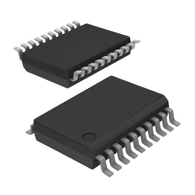
| 产品图片 |
|
| rohs | 符合RoHS无铅 / 符合限制有害物质指令(RoHS)规范要求 |
| 产品系列 | 接口 IC,RS-422接口集成电路,Exar SP26LV431CN-L- |
| 数据手册 | http://www.exar.com/Common/Content/Document.ashx?id=758 |
| 产品型号 | SP26LV431CN-L |
| 产品种类 | RS-422接口集成电路 |
| 传播延迟时间ns | 11 ns |
| 供应商器件封装 | 16-SOIC |
| 关闭 | No |
| 其它名称 | 1016-1040-5 |
| 功能 | Transceiver |
| 包装 | 管件 |
| 协议 | RS422 |
| 双工 | - |
| 商标 | Exar |
| 安装类型 | 表面贴装 |
| 安装风格 | SMD/SMT |
| 封装/外壳 | 16-SOIC(0.154",3.90mm 宽) |
| 封装/箱体 | SOIC-16 Narrow |
| 工作温度 | 0°C ~ 70°C |
| 工作电源电压 | 3.3 V |
| 工厂包装数量 | 49 |
| 接收器滞后 | - |
| 接收机数量 | 10 |
| 数据速率 | 60Mbps |
| 最大功率耗散 | 1100 mW |
| 最大工作温度 | + 70 C |
| 最小工作温度 | 0 C |
| 标准包装 | 49 |
| 激励器数量 | 4 |
| 电压-电源 | 3.3V |
| 电源电流 | 100 uA |
| 类型 | 驱动器 |
| 输出电压 | 2.9 V |
| 输出电流 | 150 mA |
| 驱动器/接收器数 | 4/0 |


- 商务部:美国ITC正式对集成电路等产品启动337调查
- 曝三星4nm工艺存在良率问题 高通将骁龙8 Gen1或转产台积电
- 太阳诱电将投资9.5亿元在常州建新厂生产MLCC 预计2023年完工
- 英特尔发布欧洲新工厂建设计划 深化IDM 2.0 战略
- 台积电先进制程称霸业界 有大客户加持明年业绩稳了
- 达到5530亿美元!SIA预计今年全球半导体销售额将创下新高
- 英特尔拟将自动驾驶子公司Mobileye上市 估值或超500亿美元
- 三星加码芯片和SET,合并消费电子和移动部门,撤换高东真等 CEO
- 三星电子宣布重大人事变动 还合并消费电子和移动部门
- 海关总署:前11个月进口集成电路产品价值2.52万亿元 增长14.8%


PDF Datasheet 数据手册内容提取
SP26LV431 HIGH SPEED +3.3V QUAD RS-422 DIFFERENTIAL LINE DRIVER JUNE 2011 REV. 1.1.1 GENERAL DESCRIPTION FEATURES The SP26LV431 is a quad differential line driver that • Quad Differential Line Drivers meets the specifications of the EIA standard RS-422 • Compatible with the EIA standard for RS-422 serial serial protocol. The SP26LV431 features Exar's protocol BiCMOS process allowing low power operational characteristics of CMOS technology while meeting all • High-Z Output Control of the demands of the RS-422 serial protocol over • At Least 60Mbps Transmission Rates 60Mbps under load. The RS-422 protocol allows up to 10 receivers to be connected to a multipoint bus • 11ns Typical Driver Propagation Delays transmission line. The SP26LV431 features a driver • Less than 1ns Typical Output Skew enable control common to all four drivers that places the output pins in a high impedance state. Since the • Single +3.3V Supply Operation cabling can be as long as 4,000 feet, the RS-422 • Common Driver Enable Control drivers of the SP26LV431 are equipped with a wide common-mode output voltage range to accommodate • Compatibility with the industry standard 26LV31 ground potential differences. • Ideal For Use with SP26LV432, Quad Receivers FIGURE 1. TYPICAL APPLICATION CIRCUIT Exar Corporation 48720 Kato Road, Fremont CA, 94538 • (510) 668-7000 • FAX (510) 668-7017 • www.exar.com
SP26LV431 HIGH SPEED +3.3V QUAD RS-422 DIFFERENTIAL LINE DRIVER REV. 1.1.1 FIGURE 2. PIN OUT ASSIGNMENT ORDERING INFORMATION OPERATING TEMPERATURE PART NUMBER PACKAGE DEVICE STATUS RANGE SP26LV431CN-L 16-pin Narrow SOIC 0°C to +70°C Active SP26LV431CN-L/TR 16-pin Narrow SOIC 0°C to +70°C Active SP26LV431EN-L 16-pin Narrow SOIC -40°C to +85°C Active SP26LV431EN-L/TR 16-pin Narrow SOIC -40°C to +85°C Active 2
SP26LV431 REV. 1.1.1 HIGH SPEED +3.3V QUAD RS-422 DIFFERENTIAL LINE DRIVER PIN DESCRIPTIONS Pin Assignments PIN NUMBER PIN NAME TYPE DESCRIPTION 1 DI1 I Driver 1 TTL input. 2 DO1A O Non-inverted driver 1 output. 3 DO1B O Inverted driver 1 output. 4 ENABLE I Driver output enable, active HIGH. 5 DO2B O Inverted driver 2 output. 6 DO2A O Non-inverted driver 2 output. 7 DI2 I Driver 2 TTL input. 8 GND Pwr Ground. 9 DI3 I Driver 3 TTL input. 10 DO3A O Non-inverted driver 3 output. 11 DO3B O Inverted driver 3 output. 12 ENABLE I Driver output enable, active LOW. 13 DO4B O Inverted driver 4 output. 14 DO4A O Non-inverted driver 4 output. 15 DI4 I Driver 4 TTL input. 16 VCC Pwr +3.0V to +3.6V power supply. Pin type: I=Input, O=Output. 3
SP26LV431 HIGH SPEED +3.3V QUAD RS-422 DIFFERENTIAL LINE DRIVER REV. 1.1.1 ABSOLUTE MAXIMUM RATINGS These are stress ratings only and functional operation of the device at these ratings or any other above those indicated in the operation sections to the specifications below is not implied. Exposure to absolute maximum rating conditions for extended periods of time may affect reliability and cause permanent damage to the device. V 0.5V to 7.0V CC V (DC Input Voltage) -1.5V to (V + 1.5V) IN CC V (DC Output Voltage) -0.5V to 7V OUT I , I (Clamp Diode Current) ±20mA IK OK I (DC Output Current, per pin) ±150mA OUT I (DC V or GND Current, per pin) ±150mA CC CC Storage Temperature Range -65°C to + 150°C Power Dissipation 16-pin PDIP 1150mW (derate 14.3mW/°C above +70°C) Power Dissipation 16-pin NSOIC 1100mW (derate 13.6mW/°C above +70°C) CAUTION: ESD (Electrostatic Discharge) sensitive device. Permanent damage may occur on unconnected devices subject to high energy electrostatic fields. Unused devices must be stored in conductive foam or shunts. Personnel should be properly grounded prior to handling this device. The protective foam should be discharged to the destination socket before devices are removed. ELECTRICAL CHARACTERISTICS UNLESS OTHERWISE NOTED: THE FOLLOWING SPECIFICATIONS APPLY FOR VCC = +3.0V TO +3.6V WITH TA = +25OC AND ALL MIN AND MAX LIMITS APPLY ACROSS THE RECOMMENDED OPERATING TEMPERATURE RANGE. SYMBOL PARAMETERS MIN. TYP. MAX. UNITS CONDITIONS V Supply Voltage 3.0 3.6 V CC V or V DC Input or Output Voltage VCC V IN OUT Input Electrical Characteristics t or t Input Rise or Fall Times 3 ns r f V HIGH Level Input Voltage 2.0 V IH V LOW Level Input Voltage 0.8 V IL Output Electrical Characteristics V HIGH Level Output Voltage 2.5 2.9 V V = V or V , I = -20mA OH IN IH IL OUT V LOW Level Output Voltage 0.2 0.5 V V = V or V , I = 20mA OL IN IH IL OUT V Differential Output Voltage 2.0 2.7 V R = 100Ω, Note 1 T L Differential Output Voltage 0.4 V R = 100Ω, Note 1 V – V L T T V Common Mode Output Voltage 3.0 V R = 100Ω, Note 1 OS L Difference in Common Mode Output 0.4 V R = 100Ω, Note 1 V –V L OS OS I Quiescent Supply Current 100 uA V = V or GND, Note 2 CC IN CC 4
SP26LV431 REV. 1.1.1 HIGH SPEED +3.3V QUAD RS-422 DIFFERENTIAL LINE DRIVER UNLESS OTHERWISE NOTED: THE FOLLOWING SPECIFICATIONS APPLY FOR VCC = +3.0V TO +3.6V WITH TA = +25OC AND ALL MIN AND MAX LIMITS APPLY ACROSS THE RECOMMENDED OPERATING TEMPERATURE RANGE. SYMBOL PARAMETERS MIN. TYP. MAX. UNITS CONDITIONS I Tri-state Output Leakage Current ±2.0 uA V = V or GND, OZ OUT CC ENABLE = V , ENABLE = V IL IH I Output Short Circuit Current -30 -150 mA V = V or GND, Notes 1 & 3 SC IN CC I Output Leakage Current Power Off 100 uA V = 0V, V = 6V, Note 1 OFF CC OUT I Output Leakage Current Power Off -100 uA V = 0V, V = -0.25V, Note OFF CC OUT 1 Switching Characteristics t , t Propagation Delays 11 18 ns Figure 5 PLHD PHLD t Skew, SP26LV431C_ 0.8 2 ns Figure 5, Note 4, SKEW tSKEW Skew, SP26LV431E_ 3 ns Figure 5, Note 4 t , t Differential Output Rise/Fall Times 4 10 ns Figure 5 TLH THL t Output Enable Time 40 ns Figure 7 PZH t Output Enable Time 40 ns Figure 7 PZL t Output Disable Time 35 ns Figure 7, Note 5 PHZ t Output Disable Time 35 ns Figure 7, Note 5 PLZ C Power Dissipation Capacitance 50 pF Note 6 PD C Input Capacitance 6 pF IN NOTE: 1. Refer to EIA specifications for RS-422 serial protocol for exact test conditions. 2. Measured per input. All other inputs at V or GND. CC 3. This is the current sourced when a high output is shorted to GND. Only one output at a time should be shorted. 4. Skew is defined as the difference in propagation delays between complementary outputs at the 50% input. 5. Output disable time is the delay from ENABLE or ENABLE being switched to the output transistors turning off. The actual disable times are less than indicated due to the delay added by the RC time constant of the load. 6. C determines the no load dynamic power consumption, P = (C V 2f) + (I V ), and the no load dynamic PD D PD CC CC CC power consumption, I = (C V f) + I . S PD CC CC 5
SP26LV431 HIGH SPEED +3.3V QUAD RS-422 DIFFERENTIAL LINE DRIVER REV. 1.1.1 FIGURE 3. SP431 BLOCK DIAGRAM FIGURE 4. AC TEST CIRCUIT 6
SP26LV431 REV. 1.1.1 HIGH SPEED +3.3V QUAD RS-422 DIFFERENTIAL LINE DRIVER FIGURE 5. PROPAGATION DELAYS FIGURE 6. DRIVER SINGLE-ENDED TRI-STATE TEST CIRCUIT 7
SP26LV431 HIGH SPEED +3.3V QUAD RS-422 DIFFERENTIAL LINE DRIVER REV. 1.1.1 FIGURE 7. DRIVER SINGLE-ENDED TRI-STATE WAVEFORMS FIGURE 8. DIFFERENTIAL RISE AND FALL TIMES 8
SP26LV431 REV. 1.1.1 HIGH SPEED +3.3V QUAD RS-422 DIFFERENTIAL LINE DRIVER 1.0 PRODUCT DESCRIPTION The SP26LV431 is a low-power quad differential line driver designed for digital data transmission meeting the specifications of the EIA standard RS-422 serial protocol. The SP26LV431 features Exar's BiCMOS process allowing low power operational characteristics of CMOS technology while meeting all of the demands of the RS-422 serial protocol up to 60Mbps under load in harsh environments. The RS-422 standard is ideal for multi-drop applications and for long-distance communication. The RS-422 protocol allows up to 10 receivers to be connected to a data bus, making it an ideal choice for multi-drop applications. Since the cabling can be as long as 4,000 feet, RS-422 drivers are equipped with a wide common mode output range to accommodate ground potential differences. Because the RS-422 is a differential interface, data is virtually immune to noise in the transmission line. The SP26LV431 accepts TTL or CMOS input levels and translates these to RS-422 output levels. The SP26LV431 features active HIGH and active LOW driver enable controls common to all four driver channels see Table 1. A logic HIGH on the ENABLE pin (pin 4) or a logic LOW on the ENABLE pin (pin 12) will enable the differential driver outputs. A logic LOW on the ENABLE pin (pin 4) and a logic HIGH on the ENABLE pin (pin 12) will force the driver outputs into high impedance (high-Z). Refer to the truth table in Table 1. All drivers are internally protected against short circuits on their outputs. The driver outputs are short-circuit limited to 150mA. The driver output skew times are typically 0.8ns. To minimize reflections, the multipoint bus transmission line should be terminated at both ends in its characteristic impedance, and stub lengths off the main line should be kept as short as possible. FIGURE 9. TWO-WIRE BALANCED SYSTEM, RS-422 TABLE 1: TRUTH TABLE, ENABLE/DISABLE FUNCTION COMMON TO ALL FOUR RS-422 DRIVERS NON-INVERTING A ENABLE ENABLE INPUT INVERTING B OUTPUT OUTPUT LOW HIGH don’t care high-Z high-Z HIGH don’t care LOW LOW HIGH don’t care LOW HIGH HIGH LOW 9
SP26LV431 HIGH SPEED +3.3V QUAD RS-422 DIFFERENTIAL LINE DRIVER REV. 1.1.1 FIGURE 10. DIFFERENTIAL PROPAGATION DELAY VS TEMPERATURE FIGURE 11. DIFFERENTIAL PROPAGATION DELAY VS VOLTAGE 10
SP26LV431 REV. 1.1.1 HIGH SPEED +3.3V QUAD RS-422 DIFFERENTIAL LINE DRIVER FIGURE 12. DIFFERENTIAL SKEW VS TEMPERATURE FIGURE 13. DIFFERENTIAL SKEW VS VOLTAGE 11
SP26LV431 HIGH SPEED +3.3V QUAD RS-422 DIFFERENTIAL LINE DRIVER REV. 1.1.1 FIGURE 14. DIFFERENTIAL TRANSITION TIME VS TEMPERATURE FIGURE 15. DIFFERENTIAL TRANSITION TIME VS VOLTAGE 12
SP26LV431 REV. 1.1.1 HIGH SPEED +3.3V QUAD RS-422 DIFFERENTIAL LINE DRIVER FIGURE 16. COMPLEMENTARY SKEW VS TEMPERATURE FIGURE 17. COMPLEMENTARY SKEW VS VOLTAGE 13
SP26LV431 HIGH SPEED +3.3V QUAD RS-422 DIFFERENTIAL LINE DRIVER REV. 1.1.1 FIGURE 18. DIFFERENTIAL VOUT VS IOUT (TEMPERATURE) FIGURE 19. DIFFERENTIAL VOUT VS IOUT (VCC) 14
SP26LV431 REV. 1.1.1 HIGH SPEED +3.3V QUAD RS-422 DIFFERENTIAL LINE DRIVER FIGURE 20. VOUT HIGH VS IOUT (TEMPERATURE) FIGURE 21. VOUT HIGH VS IOUT (VCC) 15
SP26LV431 HIGH SPEED +3.3V QUAD RS-422 DIFFERENTIAL LINE DRIVER REV. 1.1.1 FIGURE 22. VOUT LOW VS CURRENT (TEMPERATURE) FIGURE 23. VOUT LOW VS CURRENT (VCC) 16
SP26LV431 REV. 1.1.1 HIGH SPEED +3.3V QUAD RS-422 DIFFERENTIAL LINE DRIVER FIGURE 24. SUPPLY CURRENT VS TEMPERATURE FIGURE 25. SUPPLY CURRENT VS VOLTAGE 17
SP26LV431 HIGH SPEED +3.3V QUAD RS-422 DIFFERENTIAL LINE DRIVER REV. 1.1.1 FIGURE 26. SUPPLY CURRENT VS DATA RATE FIGURE 27. ICC (LOADED) VS DATA RATE 18
SP26LV431 REV. 1.1.1 HIGH SPEED +3.3V QUAD RS-422 DIFFERENTIAL LINE DRIVER FIGURE 28. SHORT CIRCUIT CURRENT VS TEMPERATURE FIGURE 29. SHORT CIRCUIT CURRENT VS VOLTAGE 19
SP26LV431 HIGH SPEED +3.3V QUAD RS-422 DIFFERENTIAL LINE DRIVER REV. 1.1.1 PACKAGE DIMENSIONS (16 PIN NSOIC) 20
SP26LV431 HIGH SPEED +3.3V QUAD RS-422 DIFFERENTIAL LINE DRIVER REV. 1.1.1 REVISION HISTORY DATE REVISION DESCRIPTION 3/08/04 A Production Release. 2/24/05 B Include tape and reel p/n’s. 9/05/08 1.0.0 Converted to Exar standard datasheet format. Add -40C to +85C temperature range option. Changed revision to 1.0.0. 2/19/09 1.1.0 Add 3ns maximum driver skew for industrial temperature option. 6/03/11 1.1.1 Remove SP26LV431CP-L option per PDN 110510-01 NOTICE EXAR Corporation reserves the right to make changes to the products contained in this publication in order to improve design, performance or reliability. EXAR Corporation assumes no responsibility for the use of any circuits described herein, conveys no license under any patent or other right, and makes no representation that the circuits are free of patent infringement. Charts and schedules contained here in are only for illustration purposes and may vary depending upon a user’s specific application. While the information in this publication has been carefully checked; no responsibility, however, is assumed for inaccuracies. EXAR Corporation does not recommend the use of any of its products in life support applications where the failure or malfunction of the product can reasonably be expected to cause failure of the life support system or to significantly affect its safety or effectiveness. Products are not authorized for use in such applications unless EXAR Corporation receives, in writing, assurances to its satisfaction that: (a) the risk of injury or damage has been minimized; (b) the user assumes all such risks; (c) potential liability of EXAR Corporation is adequately protected under the circumstances. Copyright 2011 EXAR Corporation Datasheet June 2011. Send your Serial Transceiver technical inquiry with technical details to: serialtechsupport@exar.com. Reproduction, in part or whole, without the prior written consent of EXAR Corporation is prohibited. 21