 Datasheet下载
- 型号: SP1002-01JTG
- 制造商: Littelfuse
- 库位|库存: xxxx|xxxx
- 要求:
| 数量阶梯 | 香港交货 | 国内含税 |
| +xxxx | $xxxx | ¥xxxx |
查看当月历史价格
查看今年历史价格
SP1002-01JTG产品简介:
ICGOO电子元器件商城为您提供SP1002-01JTG由Littelfuse设计生产,在icgoo商城现货销售,并且可以通过原厂、代理商等渠道进行代购。 SP1002-01JTG价格参考。LittelfuseSP1002-01JTG封装/规格:TVS - 二极管, 。您可以下载SP1002-01JTG参考资料、Datasheet数据手册功能说明书,资料中有SP1002-01JTG 详细功能的应用电路图电压和使用方法及教程。
Littelfuse Inc.生产的SP1002-01JTG是一款TVS(瞬态电压抑制)二极管,主要应用于各种电子设备中以提供过电压保护。该型号的二极管具有快速响应时间和低电容特性,使其在高速数据线和信号线的保护中表现出色。

 应用场景:

1. 通信设备:
   - 在手机、路由器、交换机等通信设备中,SP1002-01JTG用于保护天线接口、USB端口和其他高速数据传输接口免受静电放电(ESD)、雷击感应脉冲和电源浪涌的影响。

2. 消费电子产品:
   - 适用于电视、音响、平板电脑等消费电子产品中的HDMI、USB、DisplayPort等接口,防止因外部环境或用户误操作引起的过电压损坏。

3. 工业控制系统:
   - 在工业自动化设备、PLC(可编程逻辑控制器)、传感器和执行器中,SP1002-01JTG可以保护控制信号线和通信总线,确保系统在恶劣环境下稳定运行。

4. 汽车电子:
   - 用于车载娱乐系统、导航系统、CAN总线等关键部件的保护,抵御由点火系统、发电机或其他电气设备产生的瞬态电压波动。

5. 医疗设备:
   - 在医疗仪器如监护仪、超声波设备等中,SP1002-01JTG为敏感电路提供可靠的过电压保护,确保设备的安全性和可靠性。

6. 物联网(IoT)设备:
   - 在智能家居、智能穿戴设备等IoT产品中,该二极管可用于保护Wi-Fi模块、蓝牙模块和Zigbee模块等无线通信接口,防止外界干扰和电压突变对设备造成损害。

7. 电力电子设备:
   - 在电源适配器、充电器等电力电子设备中,SP1002-01JTG可以保护输入输出端口,防止由于电网波动或插拔瞬间产生的电压尖峰导致的元件损坏。

总之,SP1002-01JTG TVS二极管凭借其卓越的性能和广泛的应用范围,成为众多电子设备中不可或缺的保护元件。
| 参数 | 数值 |
| 产品目录 | |
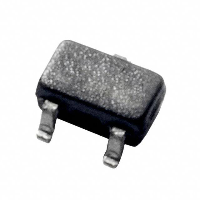
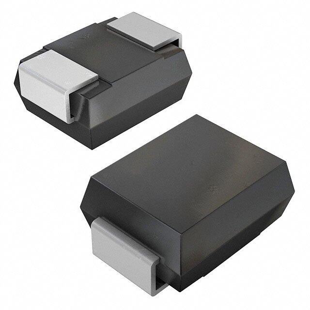
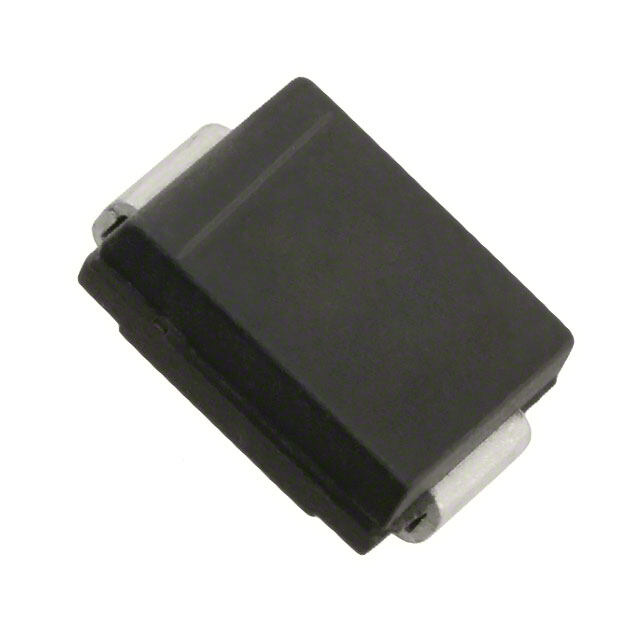
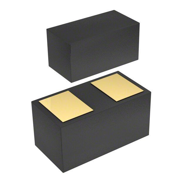
| 描述 | TVS DIODE 6VWM 16VC SC703TVS 二极管 - 瞬态电压抑制器 1 channel bi-directional |
| 产品分类 | |
| 品牌 | Littelfuse Inc |
| 产品手册 | |
| 产品图片 |
|
| rohs | 符合RoHS无铅 / 符合限制有害物质指令(RoHS)规范要求 |
| 产品系列 | 二极管与整流器,TVS二极管,TVS 二极管 - 瞬态电压抑制器,Littelfuse SP1002-01JTGSP1002, SPA® |
| 数据手册 | |
| 产品型号 | SP1002-01JTG |
| 不同频率时的电容 | - |
| 产品培训模块 | http://www.digikey.cn/PTM/IndividualPTM.page?site=cn&lang=zhs&ptm=22970http://www.digikey.cn/PTM/IndividualPTM.page?site=cn&lang=zhs&ptm=25590 |
| 产品目录绘图 |
|
| 产品目录页面 | |
| 产品种类 | TVS 二极管 - 瞬态电压抑制器 |
| 供应商器件封装 | SC-70-3 |
| 其它名称 | F2899TR |
| 击穿电压 | 6 V |
| 功率-峰值脉冲 | - |
| 包装 | 带卷 (TR) |
| 单向通道 | - |
| 双向通道 | 1 |
| 商标 | Littelfuse |
| 商标名 | SPA |
| 安装类型 | 表面贴装 |
| 安装风格 | SMD/SMT |
| 封装 | Reel |
| 封装/外壳 | SC-70,SOT-323 |
| 封装/箱体 | SC-70-3 |
| 尺寸 | 1.35 mm W x 2.25 mm L x 1 mm H |
| 峰值浪涌电流 | 2 A |
| 工作温度 | -40°C ~ 125°C |
| 工作电压 | 6 V |
| 工厂包装数量 | 3000 |
| 应用 | 通用 |
| 最大工作温度 | + 85 C |
| 最小工作温度 | - 40 C |
| 极性 | Bidirectional |
| 标准包装 | 3,000 |
| 特色产品 | http://www.digikey.com/cn/zh/ph/Littelfuse/SP1000.html |
| 电压-击穿(最小值) | 8V |
| 电压-反向关态(典型值) | 6V (最小值) |
| 电压-箝位(最大值)@Ipp | 16V |
| 电容 | 5 pF |
| 电流-峰值脉冲(10/1000µs) | 2A (8/20µs) |
| 电源线路保护 | 无 |
| 端接类型 | SMD/SMT |
| 类型 | 齐纳 |
| 系列 | SP1002 |
| 钳位电压 | 11.2 V |


- 商务部:美国ITC正式对集成电路等产品启动337调查
- 曝三星4nm工艺存在良率问题 高通将骁龙8 Gen1或转产台积电
- 太阳诱电将投资9.5亿元在常州建新厂生产MLCC 预计2023年完工
- 英特尔发布欧洲新工厂建设计划 深化IDM 2.0 战略
- 台积电先进制程称霸业界 有大客户加持明年业绩稳了
- 达到5530亿美元!SIA预计今年全球半导体销售额将创下新高
- 英特尔拟将自动驾驶子公司Mobileye上市 估值或超500亿美元
- 三星加码芯片和SET,合并消费电子和移动部门,撤换高东真等 CEO
- 三星电子宣布重大人事变动 还合并消费电子和移动部门
- 海关总署:前11个月进口集成电路产品价值2.52万亿元 增长14.8%


PDF Datasheet 数据手册内容提取
TVS Diode Array General Purpose ESD Protection - SP1002 Series SP1002 Series 5pF 8kV Bidirectional TVS Array RoHS Pb GREEN Description Back-to-Back Zener diodes fabricated in a proprietary silicon avalanche technology protect each I/O pin to provide a high level of protection for electronic equipment that may experience destructive electrostatic discharges (ESD). These robust diodes can safely absorb repetitive ESD strikes at the maximum level specified in the IEC 61000-4- 2 international standard (Level 4, ±8kV contact discharge) without performance degradation. Their very low loading capacitance also makes them ideal for protecting high- speed signal pins. Pinout Features SP1002-01JTG SP1002-02JTG • Low capacitance of 5pF • Small package saves (TYP) I/O to I/O board space (SC70-3) (SC70-5) • ESD protection of ±8kV • Lightning Protection, IEC 1 1 5 contact discharge, ±15kV 61000-4-5, 2nd edition 2A air discharge, (Level 4, (8/20µs) NC NC IEC 61000-4-2) • RoHS compliant and lead • EFT protection, IEC free 2 3 4 61000-4-4, 40A • AEC-Q101 qualified (5/50ns) • Low leakage current of 0.5μA (MAX) at 5V Functional Block Diagram Applications SP1002-01JTG SP1002-02JTG • Computer Peripherals • LCD/PDP TVs • Mobile Phones • Set Top Boxes 1 1 3 • Digital Cameras • DVD Players • Desktops/Notebooks • MP3/PMP Application Example 2 5 4 MultiMedia MultiMedia Device Device Audio Out L Audio In L Additional Information Audio Out R Audio In R 2 x SP1002-01 Datasheet Resources Samples SCART MultiMedia Application of SP1002-01 Life Support Note: Not Intended for Use in Life Support or Life Saving Applications The products shown herein are not designed for use in life sustaining or life saving applications unless otherwise expressly indicated. © 2019 Littelfuse, Inc. Specifications are subject to change without notice. Revised: 09/06/19
TVS Diode Array General Purpose ESD Protection - SP1002 Series Absolute Maximum Ratings Thermal Information Symbol Parameter Value Units Parameter Rating Units I Peak Current (t=8/20μs) 2 A Storage Temperature Range –55 to 150 °C PP p T Operating Temperature –40 to 125 °C Maximum Junction Temperature 150 °C OP T Storage Temperature –55 to 150 °C Maximum Lead Temperature 260 °C STOR (Soldering 20-40s) CAUTION: Stresses above those listed in “Absolute Maximum Ratings” may cause permanent damage to the device. This is a stress only rating and operation of the device at these or any other conditions above those indicated in the operational sections of this specification is not implied. Electrical Characteristics (T = 25°C) OP Parameter Symbol Test Conditions Min Typ Max Units Voltage Drop V I=1mA 6.0 9.5 V D R Reverse Standoff Voltage V I≤1µA with 1 I/O at GND 6.0 V RWM R Leakage Current I V=5V with I/O at GND 0.5 µA LEAK R I =1A, t=8/20µs, Fwd 9.2 13.0 V Clamp Voltage1 V PP p C I =2A, t=8/20µs, Fwd 11.2 16.0 V PP p Dynamic Resistance R (V - V ) / (I - I ) 2.0 Ω DYN C2 C1 PP2 PP1 IEC61000-4-2 (Contact) ±8 kV ESD Withstand Voltage1,2 V ESD IEC61000-4-2 (Air) ±15 kV Reverse Bias=0V 6 pF Diode Capacitance1 C Reverse Bias=2.5V 5 pF D Reverse Bias=5V 5 pF Notes: 1 Parameter is guaranteed by device characterization 2 A minimum of 1,000 ESD pulses are applied at 1s intervals Soldering Parameters Reflow Condition Pb – Free assembly - Temperature Min (T ) 150°C tP s(min) TP CCrriittiiccaall ZZoonnee Pre Heat - Temperature Max (Ts(max)) 200°C e RRaammpp--uupp TTLL ttoo TTPP Average ram-p T uimp er a(tme i(nL itqou midauxs)) T(tes)mp (TL) to peak 36°0C –/ s1e8c0o nsde cmsax rutare TS(mTaxL) tL T to T - Ramp-up Rate 3°C/second max pm RRaammpp--ddoown S(max) L e PPrreehheeaatt - Temperature (T) (Liquidus) 217°C T Reflow L TS(min) - Temperature (tL) 60 – 150 seconds tS Peak Temperature (T) 260+0/-5 °C P 25 Time within 5°C of actual peak Temperature (tp) 20 – 40 seconds time to peak temperature Time Ramp-down Rate 6°C/second max Time 25°C to peak Temperature (T) 8 minutes max. P Do not exceed 260°C © 2019 Littelfuse, Inc. Specifications are subject to change without notice. Revised: 09/06/19
TVS Diode Array General Purpose ESD Protection - SP1002 Series Package Dimensions — SC70-3 B Solder Pad Layout Package SC70-3 3 1.30 Pins 3 [0.0512] 0.65 JEDEC MO-203 E HE [0.0256] Millimeters Inches 0.70 Symbol [0.0276] Min Max Min Max 1 2 A 0.80 1.10 0.031 0.043 e e A1 0.00 0.10 0.000 0.004 A2 0.70 1.00 0.028 0.039 D B 0.15 0.30 0.006 0.012 8] 9074 c 0.08 0.25 0.003 0.010 A2 A 1.0.0 [ D 1.85 2.25 0.073 0.089 E 1.15 1.35 0.045 0.053 A1 e 0.66 BSC 0.026 BSC HE 2.00 2.40 0.079 0.094 4] C 0.900.035 L 0.26 0.46 0.010 0.018 [ L Package Dimensions — SC70-5 e e Package SC70-5 6 5 4 Pins 5 not used Solder Pad Layout JEDEC MO-203 E HE Millimeters Inches Symbol Min Max Min Max 1 2 3 A 0.80 1.10 0.031 0.043 B A1 0.00 0.10 0.000 0.004 A2 0.70 1.00 0.028 0.039 D B 0.15 0.30 0.006 0.012 A2 A c 0.08 0.25 0.003 0.010 D 1.85 2.25 0.073 0.089 A1 E 1.15 1.35 0.045 0.053 e 0.65 BSC 0.026 BSC C HE 2.00 2.40 0.079 0.094 L 0.26 0.46 0.010 0.018 L Product Characteristics Lead Plating Matte Tin Lead Material Copper Alloy Lead Coplanarity 0.0004 inches (0.102mm) Substitute Material Silicon Body Material Molded Epoxy Flammability UL 94 V-0 Notes : 1. All dimensions are in millimeters 2. Dimensions include solder plating. 3. Dimensions are exclusive of mold flash & metal burr. 4. Blo is facing up for mold and facing down for trim/form, i.e. reverse trim/form. 5. Package surface matte finish VDI 11-13. © 2019 Littelfuse, Inc. Specifications are subject to change without notice. Revised: 09/06/19
TVS Diode Array General Purpose ESD Protection - SP1002 Series Part Numbering System Part Marking System SP 1002 – ** J T G B* * B** Product Series Number of Channels TVS Diode Arrays G= Green B = SP1002 Series (varies) (SPA® Diodes) T= Tape & Reel Assembly Site (varies) Series Ordering Information Number of Channels Package -01 = 1 Channel J = SC70-3 Part Number Package Marking Min. Order Qty. -02 = 2 Channel SC70-5 SP1002-01JTG SC70-3 B*1 3000 SP1002-02JTG SC70-5 B*2 3000 Embossed Carrier Tape & Reel Specification — SC70-3 PO Millimetres Inches Symbol P2 ØD t Min Max Min Max E 1.65 1.85 0.065 0.073 E F 3.45 3.55 0.135 0.139 P2 1.95 2.05 0.077 0.081 W D 1.40 1.60 0.055 0.063 D1 1.00 1.25 0.039 0.049 F P0 3.90 4.10 0.154 0.161 ØD1 BOB1 K1 10P0 40.0 ± 0.20 1.574 ± 0.008 W 7.70 8.10 0.303 0.318 AO P P 3.90 4.10 0.153 0.161 A1 A0 2.30 2.50 0.090 0.098 A1 1.00 Ref 0.039 Ref B0 2.30 2.50 0.090 0.098 O B1 1.90 Ref 0.074 K K0 1.10 1.30 0.043 0.051 K1 0.60 Ref 0.023 Ref t 0.27 max 0.010 Embossed Carrier Tape & Reel Specification — SC70-5 and SC70-6 Millimetres Inches Symbol Min Max Min Max E 1.65 1.85 0.065 0.073 F 3.45 3.55 0.135 0.139 P2 1.95 2.05 0.077 0.081 D 1.40 1.60 0.055 0.063 D1 1.00 1.25 0.039 0.049 P0 3.90 4.10 0.154 0.161 10P0 40.0 ± 0.20 1.574 ± 0.008 W 7.70 8.10 0.303 0.318 P 3.90 4.10 0.153 0.161 A0 2.14 2.34 0.084 0.092 B0 2.24 2.44 0.088 0.096 K0 1.12 1.32 0.044 0.052 t 0.27 max 0.010 max Disclaimer Notice - Information furnished is believed to be accurate and reliable. However, users should independently evaluate the suitability of and test each product selected for their own applications. Littelfuse products are not designed for, and may not be used in, all applications. Read complete Disclaimer Notice at www.littelfuse.com/disclaimer-electronics. © 2019 Littelfuse, Inc. Specifications are subject to change without notice. Revised: 09/06/19