ICGOO在线商城 > 集成电路(IC) > 接口 - 驱动器,接收器,收发器 > SN75LVDS83ADGG

 Datasheet下载
- 型号: SN75LVDS83ADGG
- 制造商: Texas Instruments
- 库位|库存: xxxx|xxxx
- 要求:
| 数量阶梯 | 香港交货 | 国内含税 |
| +xxxx | $xxxx | ¥xxxx |
查看当月历史价格
查看今年历史价格
SN75LVDS83ADGG产品简介:
ICGOO电子元器件商城为您提供SN75LVDS83ADGG由Texas Instruments设计生产,在icgoo商城现货销售,并且可以通过原厂、代理商等渠道进行代购。 SN75LVDS83ADGG价格参考。Texas InstrumentsSN75LVDS83ADGG封装/规格:接口 - 驱动器,接收器,收发器, 驱动器 5/0 LVDS 56-TSSOP。您可以下载SN75LVDS83ADGG参考资料、Datasheet数据手册功能说明书,资料中有SN75LVDS83ADGG 详细功能的应用电路图电压和使用方法及教程。
Texas Instruments(德州仪器)的SN75LVDS83ADGG是一款低电压差分信号(LVDS)收发器,广泛应用于需要高速、低功耗和低电磁干扰(EMI)的接口通信场景中。以下是该型号的具体应用场景:

 1. 工业自动化与控制
   在工业环境中,SN75LVDS83ADGG常用于连接传感器、执行器和其他控制系统之间的数据传输。由于其高速率和抗噪性能,它能够确保在复杂的工业环境下实现稳定的数据传输。例如,在工厂自动化系统中,它可以用于连接PLC(可编程逻辑控制器)与远程设备之间的通信。

 2. 显示与视频传输
   SN75LVDS83ADGG适用于液晶显示器(LCD)、有机发光二极管(OLED)等显示面板的驱动电路中。它能够以高速率传输图像数据,支持高分辨率显示,并且其低功耗特性有助于延长电池寿命,特别适合便携式设备如平板电脑、智能手机等。

 3. 通信设备
   在通信领域,SN75LVDS83ADGG可用于路由器、交换机、基站等设备中的背板通信。它支持长距离、高速率的数据传输,同时保持较低的功耗和电磁干扰,确保通信系统的稳定性和可靠性。

 4. 汽车电子
   随着汽车智能化的发展,SN75LVDS83ADGG在车载信息娱乐系统、摄像头模块、驾驶辅助系统(如ADAS)中得到广泛应用。它能够在恶劣的车内外环境中提供可靠的高速数据传输,支持多个摄像头和传感器之间的同步通信。

 5. 医疗设备
   在医疗成像设备如超声波机、CT扫描仪等中,SN75LVDS83ADGG用于图像数据的高速传输。其低噪声和高可靠性特性确保了医疗设备的精确性和安全性。

 6. 消费电子
   在智能家居、安防监控等领域,SN75LVDS83ADGG可以用于摄像头、传感器与中央处理单元之间的数据传输。它的低功耗和高速率特性使其成为这些应用的理想选择。

总之,SN75LVDS83ADGG凭借其卓越的性能和广泛的适用性,成为许多高性能、低功耗应用的理想选择。
| 参数 | 数值 |
| 产品目录 | 集成电路 (IC)半导体 |
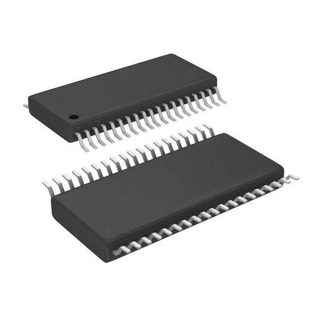
| 描述 | IC FLATLINK TRANSMITTER 56TSSOP总线发射器 Flatlink 10-100MHz Transmitter |
| 产品分类 | |
| 品牌 | Texas Instruments |
| 产品手册 | |
| 产品图片 |
|
| rohs | 符合RoHS无铅 / 符合限制有害物质指令(RoHS)规范要求 |
| 产品系列 | 逻辑集成电路,总线发射器,Texas Instruments SN75LVDS83ADGGFlatLink™ |
| 数据手册 | |
| 产品型号 | SN75LVDS83ADGG |
| 产品目录页面 | |
| 产品种类 | 总线发射器 |
| 供应商器件封装 | 56-TSSOP |
| 其它名称 | 296-24867-5 |
| 包装 | 管件 |
| 协议 | LVDS |
| 单位重量 | 252.800 mg |
| 双工 | - |
| 商标 | Texas Instruments |
| 安装类型 | 表面贴装 |
| 安装风格 | SMD/SMT |
| 封装 | Tube |
| 封装/外壳 | 56-TFSOP(0.240",6.10mm 宽) |
| 封装/箱体 | TSSOP-56 |
| 工作温度 | -10°C ~ 70°C |
| 工厂包装数量 | 35 |
| 接收器滞后 | - |
| 数据速率 | - |
| 最大功率耗散 | 1111 mW |
| 最大工作温度 | + 70 C |
| 最小工作温度 | - 10 C |
| 标准包装 | 35 |
| 电压-电源 | 3 V ~ 3.6 V |
| 电源电压-最大 | 3.6 V |
| 电源电压-最小 | 3 V |
| 类型 | 驱动器 |
| 系列 | SN75LVDS83A |
| 驱动器/接收器数 | 5/0 |


- 商务部:美国ITC正式对集成电路等产品启动337调查
- 曝三星4nm工艺存在良率问题 高通将骁龙8 Gen1或转产台积电
- 太阳诱电将投资9.5亿元在常州建新厂生产MLCC 预计2023年完工
- 英特尔发布欧洲新工厂建设计划 深化IDM 2.0 战略
- 台积电先进制程称霸业界 有大客户加持明年业绩稳了
- 达到5530亿美元!SIA预计今年全球半导体销售额将创下新高
- 英特尔拟将自动驾驶子公司Mobileye上市 估值或超500亿美元
- 三星加码芯片和SET,合并消费电子和移动部门,撤换高东真等 CEO
- 三星电子宣布重大人事变动 还合并消费电子和移动部门
- 海关总署:前11个月进口集成电路产品价值2.52万亿元 增长14.8%


PDF Datasheet 数据手册内容提取
Product Sample & Technical Tools & Support & Folder Buy Documents Software Community SN75LVDS83A SLLS980E–JUNE2009–REVISEDNOVEMBER2016 SN75LVDS83A Flatlink™ Transmitter 1 Features 3 Description • LVDSDisplaySerDesInterfacesDirectlytoLCD The SN75LVDS83A Flatlink™ transmitter device 1 contains four 7-bit parallel-load serial-out shift DisplayPanelswithIntegratedLVDS registers, a 7× clock synthesizer, and five Low- • PackageOptions:8.1mm ×14mmTSSOP Voltage Differential Signaling (LVDS) line drivers in a • 3.3-VTolerantDataInputs single integrated circuit. These functions allow 28 bits • TransferRateupto100Mpps(MegaPixelPer of single-ended LVTTL data to be synchronously transmitted over five balanced-pair conductors for Second) receipt by a compatible receiver, such as the • PixelClockFrequencyRange:10MHzto100 SN75LVDS82 and LCD panels with integrated LVDS MHz receiver. • SuitedforDisplayResolutionsRangingFrom When transmitting, data bits D0 through D27 are HVGAuptoHDWithLowEMI each loaded into registers upon the edge of the input • OperatesFromaSingle3.3-VSupplyand clock signal (CLKIN). The rising or falling edge of the 170mW(Typical)at75MHz clock can be selected via the clock select (CLKSEL) • 28DataChannelsPlusClockInLow-VoltageTTL pin. The frequency of CLKIN is multiplied seven times, and then used to unload the data registers in to4DataChannelsPlusClockOutLow-Voltage 7-bit slices and serially. The four serial streams and a Differential phase-locked clock (CLKOUT) are then output to • ConsumesLessThan1mWWhenDisabled LVDS output drivers. The frequency of CLKOUT is • SelectableRisingorFallingClockEdgeTriggered thesameastheinputclock,CLKIN. Inputs DeviceInformation(1) • ESD:5000VHBM PARTNUMBER PACKAGE BODYSIZE(NOM) • SupportSpreadSpectrumClocking(SSC) SN75LVDS83A TSSOP(56) 14.00mm×6.10mm • CompatibleWithallOMAP™2x,OMAP™3x,and DaVinci™ApplicationProcessors (1) For all available packages, see the orderable addendum at theendofthedatasheet. 2 Applications • Tablets • IndustrialPC,Laptop,andOtherFactory AutomationDisplays • PatientMonitorandMedicalEquipmentDisplays • ElectronicPoint-of-Sale(EPOS)Displays • PrinterDisplays LVDSApplication swivel Application processor SN75LVDS83A (e.g. OMAPTM) FlatLinkTMTransmitter TSSOP: 8 x 14mm DGG 1 An IMPORTANT NOTICE at the end of this data sheet addresses availability, warranty, changes, use in safety-critical applications, intellectualpropertymattersandotherimportantdisclaimers.PRODUCTIONDATA.
SN75LVDS83A SLLS980E–JUNE2009–REVISEDNOVEMBER2016 www.ti.com Table of Contents 1 Features.................................................................. 1 9.1 Overview.................................................................14 2 Applications........................................................... 1 9.2 FunctionalBlockDiagram.......................................14 3 Description............................................................. 1 9.3 FeatureDescription.................................................15 9.4 DeviceFunctionalModes........................................16 4 RevisionHistory..................................................... 2 10 ApplicationandImplementation........................ 17 5 Description(continued)......................................... 3 10.1 ApplicationInformation..........................................17 6 PinConfigurationandFunctions......................... 3 10.2 TypicalApplication................................................23 7 Specifications......................................................... 6 11 PowerSupplyRecommendations..................... 27 7.1 AbsoluteMaximumRatings .....................................6 12 Layout................................................................... 27 7.2 ESDRatings..............................................................6 12.1 LayoutGuidelines.................................................27 7.3 RecommendedOperatingConditions.......................6 12.2 LayoutExample....................................................29 7.4 ThermalInformation..................................................6 13 DeviceandDocumentationSupport................. 31 7.5 ElectricalCharacteristics...........................................7 7.6 DissipationRatings...................................................7 13.1 ReceivingNotificationofDocumentationUpdates31 7.7 TimingRequirements................................................8 13.2 CommunityResources..........................................31 7.8 SwitchingCharacteristics..........................................8 13.3 Trademarks...........................................................31 7.9 TypicalCharacteristics............................................10 13.4 ElectrostaticDischargeCaution............................31 13.5 Glossary................................................................31 8 ParameterMeasurementInformation................11 14 Mechanical,Packaging,andOrderable 9 DetailedDescription............................................ 14 Information........................................................... 31 4 Revision History NOTE:Pagenumbersforpreviousrevisionsmaydifferfrompagenumbersinthecurrentversion. ChangesfromRevisionD(June2011)toRevisionE Page • AddedESDRatingstable,FeatureDescriptionsection,DeviceFunctionalModes,ApplicationandImplementation section,PowerSupplyRecommendationssection,Layoutsection,DeviceandDocumentationSupportsection,and Mechanical,Packaging,andOrderableInformationsection.................................................................................................. 1 • DeletedOrderingInformationtable;seePOAattheendofthedatasheet........................................................................... 1 • AddedThermalInformationtable........................................................................................................................................... 6 ChangesfromRevisionC(August2009)toRevisionD Page • Changed24-BitColorHostto24-bitLCDPanelApplicationSchematicFrom:G7(LSB)To:G7(MSB)............................. 18 ChangesfromRevisionB(July2009)toRevisionC Page • DeletedsentenceinthePinFunctionstableforentryD0-D27-"supports1.8Vto3.3Vinputvoltageselectableby VDDsupply.".......................................................................................................................................................................... 4 ChangesfromRevisionA(June2009)toRevisionB Page • ChangedthedatasheetFrom:ProductPreviewTo:Production........................................................................................... 1 ChangesfromOriginal(June2009)toRevisionA Page • ChangedDescriptiontextFrom:Alternativedeviceoption:TheSN75LVDS83Aisanalternative...To:Alternative deviceoption:TheSN75LVDS83Bisanalternative.............................................................................................................. 3 • ChangedTypicalPRBSOutputSignalvsOverOneClockPeriodgraph............................................................................ 10 2 SubmitDocumentationFeedback Copyright©2009–2016,TexasInstrumentsIncorporated ProductFolderLinks:SN75LVDS83A
SN75LVDS83A www.ti.com SLLS980E–JUNE2009–REVISEDNOVEMBER2016 5 Description (continued) The SN75LVDS83A requires no external components and little or no control. The data bus appears the same at the input to the transmitter and output of the receiver with the data transmission transparent to the user(s). The only user intervention is selecting a clock rising edge by inputting a high level to CLKSEL or a falling edge with a low-level input, and the possible use of the Shutdown/Clear (SHTDN). SHTDN is an active-low input to inhibit the clock, and shut off the LVDS output drivers for lower power consumption. A low-level on this signal clears all internalregisterstoalow-level. TheSN75LVDS83Aischaracterizedforoperationoverambientairtemperaturesof –10°Cto70°C. Alternative device option: The SN75LVDS83B is an alternative to the SN75LVDS83A for clock frequency range of 10 MHz to 135 MHz. The SN75LVDS83B is available in a smaller BGA package in addition to the TSSOP package. 6 Pin Configuration and Functions DGGPackage 56-PinTSSOP TopView VCC 1 56 D4 D5 2 55 D3 D6 3 54 D2 D7 4 53 GND GND 5 52 D1 D8 6 51 D0 D9 7 50 D27 D10 8 49 GND VCC 9 48 Y0M D11 10 47 Y0P D12 11 46 Y1M D13 12 45 Y1P GND 13 44 LVDSVCC D14 14 43 GND D15 15 42 Y2M D16 16 41 Y2P CLKSEL 17 40 CLKOUTM D17 18 39 CLKOUTP D18 19 38 Y3M D19 20 37 Y3P GND 21 36 GND D20 22 35 GND D21 23 34 PLLVCC D22 24 33 GND D23 25 32 SHTDN VCC 26 31 CLKIN D24 27 30 D26 D25 28 29 GND Copyright©2009–2016,TexasInstrumentsIncorporated SubmitDocumentationFeedback 3 ProductFolderLinks:SN75LVDS83A
SN75LVDS83A SLLS980E–JUNE2009–REVISEDNOVEMBER2016 www.ti.com PinFunctions PIN TYPE(1) DESCRIPTION NAME NO. CMOSwithpulldown;inputpixelclock;risingorfallingclockpolarityisselectableby CLKIN 31 I ControlinputCLKSEL. CLKOUTM 40 O DifferentialLVDSpixelclockoutput. CLKOUTP 39 O Outputishigh-impedancewhenSHTDNispulledlow(de-asserted). CMOSwithpulldown;selectsbetweenrisingedgeinputclocktrigger(CLKSEL=V ) CLKSEL 17 I IH andfallingedgeinputclocktrigger(CLKSEL=V ). IL D0 51 I D1 52 I D2 54 I D3 55 I D4 56 I D5 2 I D6 3 I D7 4 I D8 6 I D9 7 I D10 8 I D11 10 I D12 11 I CMOSwithpulldown;datainputs.Toconnectagraphicsourcesuccessfullytoadisplay, D13 12 I thebitassignmentofD[27:0]iscritical(andnotnecessarilyintuitive). Forinputbitassignment,seeFigure14toFigure17fordetails. D14 14 I Note:ifapplicationonlyrequires18-bitcolor,connectunusedinputsD5,D10,D11,D16, D15 15 I D17,D23,andD27toGND. D16 16 I D17 18 I D18 19 I D19 20 I D20 22 I D21 23 I D22 24 I D23 25 I D24 27 I D25 28 I D26 30 I D27 50 I GND 5,23,21,29, P SupplygroundforVCC,LVDSVCC,andPLLVCC(2) 43,49,53 LVDSVCC 44 P 3.3-VLVDSoutputanalogsupply(2) PLLVCC 34 P 3.3-VPLLanalogsupply(2) CMOSwithpulldown;deviceshutdown;pulllow(deassert)toshutdownthedevice(low SHTDN 32 I power,resetsallregisters)andhigh(assert)fornormaloperation. VCC 1,9,26 P 3.3-Vdigitalsupplyvoltage(2) DifferentialLVDSdataoutputs.Outputishigh-impedancewhenSHTDNispulledlow Y0M 48 O (deasserted). DifferentialLVDSdataoutputs.Outputishigh-impedancewhenSHTDNispulledlow Y0P 47 O (deasserted). (1) I=Input,O=Output,P=Power (2) Foramulti-layerPCB,TIrecommendskeepingonecommonGNDlayerunderneaththedeviceandconnectingallgroundterminals directlytothisplane. 4 SubmitDocumentationFeedback Copyright©2009–2016,TexasInstrumentsIncorporated ProductFolderLinks:SN75LVDS83A
SN75LVDS83A www.ti.com SLLS980E–JUNE2009–REVISEDNOVEMBER2016 PinFunctions(continued) PIN TYPE(1) DESCRIPTION NAME NO. DifferentialLVDSdataoutputs.Outputishigh-impedancewhenSHTDNispulledlow Y1M 46 O (deasserted). DifferentialLVDSdataoutputs.Outputishigh-impedancewhenSHTDNispulledlow Y1P 45 O (deasserted). DifferentialLVDSdataoutputs.Outputishigh-impedancewhenSHTDNispulledlow Y2M 42 O (deasserted). DifferentialLVDSdataoutputs.Outputishigh-impedancewhenSHTDNispulledlow Y2P 41 O (deasserted). DifferentialLVDSDataoutputs.Outputishigh-impedancewhenSHTDNispulledlow Y3M 38 O (deasserted). Note:Iftheapplicationonlyrequires18-bitcolor,thisoutputcanbeleftopen. DifferentialLVDSDataoutputs.Outputishigh-impedancewhenSHTDNispulledlow Y3P 37 O (deasserted). Note:Iftheapplicationonlyrequires18-bitcolor,thisoutputcanbeleftopen. Copyright©2009–2016,TexasInstrumentsIncorporated SubmitDocumentationFeedback 5 ProductFolderLinks:SN75LVDS83A
SN75LVDS83A SLLS980E–JUNE2009–REVISEDNOVEMBER2016 www.ti.com 7 Specifications 7.1 Absolute Maximum Ratings(1) MIN MAX UNIT Supplyvoltage,VCC,LVDSVCC,PLLVCC(2) –0.5 4 V Voltageatanyoutputterminal –0.5 VCC+0.5 V Voltageatanyinputterminal –0.5 VCC+0.5 V Continuouspowerdissipation SeeDissipationRatings Storagetemperature,T –65 150 °C stg (1) StressesbeyondthoselistedunderAbsoluteMaximumRatingsmaycausepermanentdamagetothedevice.Thesearestressratings only,whichdonotimplyfunctionaloperationofthedeviceattheseoranyotherconditionsbeyondthoseindicatedunderRecommended OperatingConditions.Exposuretoabsolute-maximum-ratedconditionsforextendedperiodsmayaffectdevicereliability. (2) AllvoltagesarewithrespecttotheGNDterminals. 7.2 ESD Ratings VALUE UNIT Human-bodymodel(HBM)(1) ±5000 V Electrostaticdischarge Charged-devicemodel(CDM)(2) ±500 V (ESD) Machinemodel(MM)(3) ±150 (1) InaccordancewithJEDECStandard22,TestMethodA114-A. (2) InaccordancewithJEDECStandard22,TestMethodC101. (3) InaccordancewithJEDECStandard22,TestMethodA115-A. 7.3 Recommended Operating Conditions overoperatingfree-airtemperaturerange(unlessotherwisenoted) MIN NOM MAX UNIT VCC Supplyvoltage 3 3.3 3.6 V LVDSVCC LVDSoutputsupplyvoltage 3 3.3 3.6 V PLLVCC PLLanalogsupplyvoltage 3 3.3 3.6 V PowersupplynoiseonanyVCCterminal 0.1 V V High-levelinputvoltage VCC/2+0.5 V IH V Low-levelinputvoltage VCC/2–0.5 V IL Z Differentialloadimpedance 90 132 Ω L T Operatingfree-airtemperature –10 70 °C A 7.4 Thermal Information SN75LVDS83A THERMALMETRIC(1) DGG(TSSOP) UNIT 56PINS R Junction-to-ambientthermalresistance 62.1 °C/W θJA R Junction-to-case(top)thermalresistance 18.5 °C/W θJC(top) R Junction-to-boardthermalresistance 31.1 °C/W θJB ψ Junction-to-topcharacterizationparameter 0.8 °C/W JT ψ Junction-to-boardcharacterizationparameter 30.8 °C/W JB R Junction-to-case(bottom)thermalresistance — °C/W θJC(bot) (1) Formoreinformationabouttraditionalandnewthermalmetrics,seetheSemiconductorandICPackageThermalMetricsapplication report. 6 SubmitDocumentationFeedback Copyright©2009–2016,TexasInstrumentsIncorporated ProductFolderLinks:SN75LVDS83A
SN75LVDS83A www.ti.com SLLS980E–JUNE2009–REVISEDNOVEMBER2016 7.5 Electrical Characteristics overoperatingfree-airtemperaturerange(unlessotherwisenoted) PARAMETER TESTCONDITIONS MIN TYP(1) MAX UNIT V Inputvoltagethreshold R =100Ω,seeFigure6 VCC/2 V T L Differentialsteady-stateoutput |V | R =100Ω,seeFigure6 250 450 mV OD voltagemagnitude L Changeinthesteady-state differentialoutputvoltage Δ|V | R =100Ω,seeFigure6 1 35 mV OD magnitudebetweenopposite L binarystates Steady-statecommon-mode V t (Dx,CLKin)=1ns,seeFigure6 1.125 1.375 V OC(SS) outputvoltage R/F Peak-to-peakcommon-mode V t (Dx,CLKin)=1ns,seeFigure6 100 mV OC(PP) outputvoltage R/F I High-levelinputcurrent V =VCC 25 µA IH IH I Low-levelinputcurrent V =0V ±10 µA IL IL V =0V ±24 mA OY I Short-circuitoutputcurrent OS V =0V ±12 mA OD High-impedancestateoutput I V =0VtoVCC ±20 µA OZ current O Inputpulldownintegrated R Dx,CLKSEL,SHTDN,CLKIN 100 kΩ pdn resistoronallinputs SHTDN=V ,disabled,allinputsat I Quiescentcurrent IL 2 100 µA Q GND SHTDN=V ,R =100Ω(5places), IH L grayscalepattern(Figure7) 52.3 62.2 mA VCC=3.3V,f =75MHz CLK SHTDN=V ,R =100Ω(5places), IH L 50%transitiondensitypattern(Figure7), 53.9 67.1 mA VCC=3.3V,f =75MHz CLK I Supplycurrent(average) CC SHTDN=V ,R =100Ω(5places), IH L worst-casepattern(Figure8), 65 79.3 mA VCC=3.6V,f =75MHz CLK SHTDN=V ,R =100Ω(5places), IH L worst-casepattern(Figure8), 96.8 mA f =100MHz CLK C Inputcapacitance 2 pF I (1) AlltypicalvaluesareatVCC=3.3V,T =25°C. A 7.6 Dissipation Ratings PACKAGE CIRCUITBOARDMODEL(1) T ≤25°C DERATINGFACTOR(2) TJA=70°C JA ABOVET =25°C POWERRATING JA Low-K 1111mW 12.3mW/°C 555mW DGG High-K 1730mW 19mW/°C 865mW (1) InaccordancewiththeHigh-KandLow-KthermalmetricdefinitionsofEIA/JESD51-2. (2) Thisistheinverseofthejunction-to-ambientthermalresistancewhenboard-mountedandwithnoairflow. Copyright©2009–2016,TexasInstrumentsIncorporated SubmitDocumentationFeedback 7 ProductFolderLinks:SN75LVDS83A
SN75LVDS83A SLLS980E–JUNE2009–REVISEDNOVEMBER2016 www.ti.com 7.7 Timing Requirements MIN MAX UNIT t Inputclockperiod 10 100 ns c withmodulationfrequency30kHz 8% Inputclockmodulation(SSC) withmodulationfrequency50kHz 6% t High-levelinputclockpulsewidthduration 0.4×t 0.6×t ns w c c t Inputsignaltransitiontime 3 ns t Datasetuptime,D0throughD27beforeCLKIN(seeFigure5) 2 ns Dataholdtime,D0throughD27afterCLKIN 0.8 ns 7.8 Switching Characteristics overoperatingfree-airtemperaturerange(unlessotherwisenoted) PARAMETER TESTCONDITIONS MIN TYP(1) MAX UNIT Delaytime,CLKOUT↑afterYnvalid t =10ns,|Inputclockjitter|<25ps t0 (serialbitposition0,equalD1,D9,D20, (CseeFigure9)(2) –0.1 0 0.1 ns D5) Delaytime,CLKOUT↑afterYnvalid t1 (serialbitposition1,equalD0,D8,D19, t(Cse=e1F0ignusr,e|I9n)p(2u)tclockjitter|<25ps 1/7tc–0.1 1/7tc+0.1 ns D27) Delaytime,CLKOUT↑afterYnvalid t2 (serialbitposition2,equalD7,D18, t(Cse=e1F0ignusr,e|I9n)p(2u)tclockjitter|<25ps 2/7tc–0.1 2/7tc+0.1 ns D26.D23) Delaytime,CLKOUT↑afterYnvalid t3 (serialbitposition3;equalD6,D15, t(Cse=e1F0ignusr,e|I9n)p(2u)tclockjitter|<25ps 3/7tc–0.1 3/7tc+0.1 ns D25,D17) Delaytime,CLKOUT↑afterYnvalid t4 (serialbitposition4,equalD4,D14, t(Cse=e1F0ignusr,e|I9n)p(2u)tclockjitter|<25ps 4/7tc–0.1 4/7tc+0.1 ns D24,D16) Delaytime,CLKOUT↑afterYnvalid t5 (serialbitposition5,equalD3,D13, t(Cse=e1F0ignusr,e|I9n)p(2u)tclockjitter|<25ps 5/7tc–0.1 5/7tc+0.1 ns D22,D11) Delaytime,CLKOUT↑afterYnvalid t =10ns, C t (serialbitposition6,equalD2,D12, |Inputclockjitter|<25ps 6/ t –0.1 6/ t +0.1 ns 6 7 c 7 c D21,D10) (seeFigure9)(2) t Outputskew,t -n/ t Targetpotentialadjustmentafter –0.1 0.1 ns sk(o) n 7 C characteristic (–0.15) (0.15) t Outputclockperiod t ns c(o) c t =10ns,cleanreferenceclock C ±40 (seeFigure10) Δt Outputclockcycle-to-cyclejitter(3) tC=10nswith0.05UIaddednoise ±44 ps c(o) modulatedat3MHz(seeFigure10) t =10nswith0.1UIaddednoise C ±42 modulatedat3MHz(seeFigure10) t High-leveloutputclockpulseduration 4/ t ns w 7 c Differentialoutputvoltagetransitiontime t fCLK(seeFigure6) 225 500 ps r/f (t ort) r f Enabletime,SHTDN↑tophaselock t f =100MHz(seeFigure11) 6 ms en (Ynvalid) CLK Disabletime,SHTDN↓tooff-state t f =100MHz(seeFigure12) 7 ns dis (CLKOUThigh-impedance) CLK (1) AlltypicalvaluesareatV =3.3V,T =25°C. CC A (2) |Inputclockjitter|isthemagnitudeofthechangeintheinputclockperiod. (3) Theoutputclockcycle-to-cyclejitteristhelargestrecordedchangeintheoutputclockperiodfromonecycletothenextcycleobserved over15,000cycles.TektronixTDSJIT3JitterAnalysissoftwarewasusedtoderivethemaximumandminimumjittervalue. 8 SubmitDocumentationFeedback Copyright©2009–2016,TexasInstrumentsIncorporated ProductFolderLinks:SN75LVDS83A
SN75LVDS83A www.ti.com SLLS980E–JUNE2009–REVISEDNOVEMBER2016 Dn CLKIN or CLKIN CLKOUT Previous cycle Current cycle Next Y0 D0-1 D7 D6 D4 D3 D2 D1 D0 D7+1 Y1 D8-1 D18 D15 D14 D13 D12 D9 D8 D18+1 Y2 D19-1 D26 D25 D24 D22 D21 D20 D19 D26+1 Y3 D27-1 D23 D17 D16 D11 D10 D5 D27 D23+1 Figure1. TypicalSN75LVDS83ALoadandShiftSequences Copyright©2009–2016,TexasInstrumentsIncorporated SubmitDocumentationFeedback 9 ProductFolderLinks:SN75LVDS83A
SN75LVDS83A SLLS980E–JUNE2009–REVISEDNOVEMBER2016 www.ti.com 7.9 Typical Characteristics 100 800 Total Device Current (Using Grayscale pattern) Over Pixel Clock Frequency Output Jitter 90 700 A nt - m 80 s-pp 600 Input Jitter e p ply Curr 7600 VCC= 3.6V k Jitter - 540000 p c u o erage S 50 eriod Cl 300 Av 40 VCC= 3.3V P 200 - CLK Frequency During Test = 100MHz C C 100 I 30 V = 3V CC 0 20 0.01 0.10 1 10 10 20 30 40 50 60 70 80 90 100 f - Input Modular Frequency - MHz f - Clock Frequency - MHz (mod) clk Figure2.AverageGrayscaleICCvsClockFrequency Figure3.OutputClockJittervsInputClockJitter CLKLSignal PRBS Data Signal v di V/ m 0 8 e - g a olt V V - Clock Signal: 100MHz t - Time - 1.2ns/div k Figure4.TypicalPRBSOutputSignalvsOverOneClockPeriod 10 SubmitDocumentationFeedback Copyright©2009–2016,TexasInstrumentsIncorporated ProductFolderLinks:SN75LVDS83A
SN75LVDS83A www.ti.com SLLS980E–JUNE2009–REVISEDNOVEMBER2016 8 Parameter Measurement Information tsu thold Dn CLKIN AllinputtimingisdefinedatIOVDD/2onaninputsignalwitha10%to90%riseorfalltimeoflessthan3ns. CLKSEL=0V. Figure5. SetUpandHoldTimeDefinition 49.9W± 1% (2 PLCS) YP V OD YM VOC 100% 80% V OD(H) 0V V OD(L) 20% 0% t t f r V OC(PP) V V OC(SS) OC(SS) 0V Figure6. TestLoadandVoltageDefinitionsforLVDSOutputs CLKIN D0,8,16 D1,9,17 D2,10,18 D3,11,19 D4-7,12-15,20-23 D24-27 The16grayscaletestpatterntestdevicepowerconsumptionforatypicaldisplaypattern. Figure7. 16GrayscaleTestPattern Copyright©2009–2016,TexasInstrumentsIncorporated SubmitDocumentationFeedback 11 ProductFolderLinks:SN75LVDS83A
SN75LVDS83A SLLS980E–JUNE2009–REVISEDNOVEMBER2016 www.ti.com Parameter Measurement Information (continued) T CLKIN EVEN Dn ODD Dn Theworst-casetestpatternproducesnearlythemaximumswitchingfrequencyforalloftheLVDSoutputs. Figure8. Worst-CasePowerTestPattern t 7 CLKIN CLKOUT t 6 t 5 t 4 t 3 t 2 t 1 t 0 Yn V OD(H) ~2.5V CLKOUT orYn 0.00V 1.40V CLKIN ~0.5V V OD(L) t7 t0-6 CLKOUTisshownwithCLKSELathigh-level. CLKINpolaritydependsonCLKSELinputlevel. Figure9. SN75LVDS83ATimingDefinitions 12 SubmitDocumentationFeedback Copyright©2009–2016,TexasInstrumentsIncorporated ProductFolderLinks:SN75LVDS83A
SN75LVDS83A www.ti.com SLLS980E–JUNE2009–REVISEDNOVEMBER2016 Parameter Measurement Information (continued) Device + Reference VCO Under Test + Modulation v(t) =Asin(2pf t) mod HP8656B Signal HP8665ASynthesized Device Under DTS2070C Generator, Signal Generator, Test Digital 0.1 MHz-990 MHz 0.1 MHz-4200 MHz TimeScope RF Output CLKIN CLKOUT Input RF Output Modulation Input Figure10. OutputClockJitterTestSetUp CLKIN Dn ten SHTDN Invalid Yn Valid Figure11. EnableTimeWaveforms CLKIN tdis SHTDN CLKOUT Figure12. DisableTimeWaveforms Copyright©2009–2016,TexasInstrumentsIncorporated SubmitDocumentationFeedback 13 ProductFolderLinks:SN75LVDS83A
SN75LVDS83A SLLS980E–JUNE2009–REVISEDNOVEMBER2016 www.ti.com 9 Detailed Description 9.1 Overview The Flatlink™ is a LVDS SerDes data transmission system. The SN75LVDS83A device takes in three (or four) data words each containing seven single-ended data bits and converts this to an LVDS serial output. Each serial output runs at seven times that of the parallel data rate. The deserializer (receiver) device operates in the reverse manner. The three (or four) LVDS serial inputs are transformed back to the original seven-bit parallel single-endeddata.Flatlink™devicesareavailablein21:3or28:4SerDesratios. The 21-bit devices are designed for 6-bit RGB video for a total of 18 bits in addition to three extra bits for horizontal synchronization, vertical synchronization, and data enable. The 28-bit devices are intended for 8-bit RGB video applications. Again, the extra four bits are for horizontal synchronization, vertical synchronization, data enable, and the remaining is the reserved bit. These 28-bit devices can also be used in 6-bit and 4-bit RGB applicationsasshowninthesubsequentsystemdiagrams. 9.2 Functional Block Diagram Parallel-Load 7-bit Shift Register D0, D1, D2, D3, 7 Y0P A,B,...G D4, D6, D7 SHIFT/LOAD Y0M >CLK Parallel-Load 7-bit Shift Register D8, D9, D12, D13, 7 Y1P A,B,...G D14, D15, D18 SHIFT/LOAD Y1M >CLK Parallel-Load 7-bit ShiftRegister D19, D20, D21, D22, 7 Y2P A,B,...G D24, D25, D26 SHIFT/LOAD Y2M >CLK Parallel-Load 7-bit Shift Register D27, D5, D10, D11, 7 Y3P A,B,...G D16,D17, D23 SHIFT/LOAD Y3M >CLK Control Logic SHTDN 7X Clock/PLL 7XCLK CLKOUTP CLKIN >CLK CLKOUTM CLKINH CLKSEL RISING/FALLING EDGE 14 SubmitDocumentationFeedback Copyright©2009–2016,TexasInstrumentsIncorporated ProductFolderLinks:SN75LVDS83A
SN75LVDS83A www.ti.com SLLS980E–JUNE2009–REVISEDNOVEMBER2016 9.3 Feature Description 9.3.1 TTLInputData The data inputs to the transmitter come from the graphics processor and consist of up to 24 bits of video information,ahorizontalsynchronizationbit,averticalsynchronizationbit,anenablebit,andasparebit. Thedatacanbeloadedintotheregistersuponeithertherisingorfallingedgeoftheinputclockselectablebythe CLKSEL pin. Data inputs are 1.8 V to 3.3 V tolerant for the SN75LVDS83A and can connect directly to low- power,low-voltageapplicationandgraphicprocessors.ThebitmappingislistedinTable1. Table1.PixelBitOrdering RED GREEN BLUE LSB R0 G0 B0 R1 G1 B1 R2 G2 B2 4-bitMSB R3 G3 B3 R4 G4 B4 6-bitMSB R5 G5 B5 R6 G6 B6 8-bitMSB R7 G7 B7 9.3.2 LVDSOutputData ThepixeldataassignmentislistedinTable2for24-bit,18-bit,and12-bitcolorhosts. Table2.PixelDataAssignment 8-BIT 4-BIT SERIAL CHANNEL DATABITS FORMAT-1(1) FORMAT-2(2) FORMAT-3(3) 6-BIT NSOTENP-LSINIZEEA(4R) LINESAIZRE(S5)TEP D0 R0 R2 R2 R0 R2 VCC D1 R1 R3 R3 R1 R3 GND D2 R2 R4 R4 R2 R0 R0 Y0 D3 R3 R5 R5 R3 R1 R1 D4 R4 R6 R6 R4 R2 R2 D6 R5 R7 R7 R5 R3 R3 D7 G0 G2 G2 G0 G2 VCC D8 G1 G3 G3 G1 G3 GND D9 G2 G4 G4 G2 G0 G0 D12 G3 G5 G5 G3 G1 G1 Y1 D13 G4 G6 G6 G4 G2 G2 D14 G5 G7 G7 G5 G3 G3 D15 B0 B2 B2 B0 B2 VCC D18 B1 B3 B3 B1 B3 GND (1) 2MSBsofeachcolortransmittedover4thserialdatachannel(Y3).DominantdataformatforLCDpanel. (2) 2LSBsofeachcolortransmittedover4thserialdatachannel.Systemdesignerneedstoverifythedataformatbycheckingwiththe LCDdisplaydatasheet. (3) 24-bitcolorhostto18-bitcolorLCDpaneldisplayapplication. (4) Increaseddynamicrangeoftheentirecolorspaceattheexpenseofnon-linearstepsizesbetweeneachstep. (5) Linearstepsizewithlessdynamicrange. Copyright©2009–2016,TexasInstrumentsIncorporated SubmitDocumentationFeedback 15 ProductFolderLinks:SN75LVDS83A
SN75LVDS83A SLLS980E–JUNE2009–REVISEDNOVEMBER2016 www.ti.com Table2.PixelDataAssignment(continued) 8-BIT 4-BIT SERIAL CHANNEL DATABITS FORMAT-1(1) FORMAT-2(2) FORMAT-3(3) 6-BIT NSOTENP-LSINIZEEA(4R) LINESAIZRE(S5)TEP D19 B2 B4 B4 B2 B0 B0 D20 B3 B5 B5 B3 B1 B1 D21 B4 B6 B6 B4 B2 B2 Y2 D22 B5 B7 B7 B5 B3 B3 D24 HSYNC HSYNC HSYNC HSYNC HSYNC HSYNC D25 VSYNC VSYNC VSYNC VSYNC VSYNC VSYNC D26 ENABLE ENABLE ENABLE ENABLE ENABLE ENABLE D27 R6 R0 GND GND GND GND D5 R7 R1 GND GND GND GND D10 G6 G0 GND GND GND GND Y3 D11 G7 G1 GND GND GND GND D16 B6 B0 GND GND GND GND D17 B7 B1 GND GND GND GND D23 RSVD RSVD GND GND GND GND CLKOUT CLKIN CLK CLK CLK CLK CLK CLK 9.4 Device Functional Modes 9.4.1 InputClockEdge The transmission of data bits D0 through D27 occurs as each are loaded into registers upon the edge of the CLKIN signal, where the rising or falling edge of the clock may be selected through CLKSEL. The selection of a clock rising edge occurs by inputting a high level to CLKSEL, which is achieved by populating pullup resistor to pull CLKSEL is high. Inputting a low level to select a clock falling edge is achieved by directly connecting CLKSELtoGND. 9.4.2 LowPowerMode TheSN75LVDS83Acanbeputinlow-powerconsumptionmodebyactive-lowinputSHTDN#. Connecting terminal SHTDN to GND inhibits the clock and shut off the LVDS output drivers for lower power consumption.Alowlevelonthissignalclearsallinternalregisterstoalowlevel. PopulateapulluptoVCConSHTDN#toenablethedevicefornormaloperation. LVDSVCC VCC 5W YnPor D or 50W YnM SHTDN 10kW 7V 300kW 7V Figure13. EquivalentInputandOutputSchematicDiagrams 16 SubmitDocumentationFeedback Copyright©2009–2016,TexasInstrumentsIncorporated ProductFolderLinks:SN75LVDS83A
SN75LVDS83A www.ti.com SLLS980E–JUNE2009–REVISEDNOVEMBER2016 10 Application and Implementation NOTE Information in the following applications sections is not part of the TI component specification, and TI does not warrant its accuracy or completeness. TI’s customers are responsible for determining suitability of components for their purposes. Customers should validateandtesttheirdesignimplementationtoconfirmsystemfunctionality. 10.1 Application Information This section provides information on device connectivity to various GPU and LCD display panels, and offers a PCBroutingexample. 10.1.1 SignalConnectivity While there is no formal industry standardized specification for the input interface of LVDS LCD panels, the industry has aligned over the years on a certain data format (bit order). Figure 14 through Figure 17 show how each signal must be connected from the graphic source through the SN75LVDS83A input, output, and LVDS LCDpanelinput.Detailednotesareprovidedwitheachfigure. Copyright©2009–2016,TexasInstrumentsIncorporated SubmitDocumentationFeedback 17 ProductFolderLinks:SN75LVDS83A
SN75LVDS83A SLLS980E–JUNE2009–REVISEDNOVEMBER2016 www.ti.com Application Information (continued) 24-bpcGPU SN75LVDS83A FORMAT1 FORMAT2 (SeeNoteA) R0(LSB) D0 D27 R1 D1 D5 R2 D2 D0 R3 D3 D1 R4 D4 D2 Y0M R5 D6 D3 Y0P 100 R6 D27 D4 tocolumn R7(MSB) D5 D6 Y1M driver G0(LSB) D7 D10 Y1P 100 GGGG1234 DDDD891123 DDDD17891 YY22MP MainboardconnectorCFaPbClePanelconnector 100C2o(tLi84nmVbbtDrippnocSpgll,)er G5 D14 D12 Y3M G6 D10 D13 Y3P 100 torowdriver G7(MSB) D11 D14 B0(LSB) D15 D16 CLKOUTM B1 D18 D17 CLKOUTP 100 B2 D19 D15 B3 D20 D18 B4 D21 D19 B5 D22 D20 24-bppLCDDisplay B6 D16 D21 B7(MSB) D17 D22 HSYNC D24 D24 VSYNC D25 D25 ENABLE D26 D26 RSVD D23 D23 CLK CLKIN CLKIN C GND SHTDNCLKSEL GND VCCPLLVCCLVDSVC 3.3V 4.8k 3.3V 3.3V Rpullup C1* C2* Rpulldown (SeeNoteB) MainBoard Copyright © 2016,Texas Instruments Incorporated A. FORMAT:Themajorityof24-bitLCDdisplaypanelsrequirethetwomostsignificantbits(2MSB)ofeachcolortobe transferredoverthe4thserialdataoutputY3.Afew24-bitLCDdisplaypanelsrequirethetwoLSBsofeachcolorto be transmitted over the Y3 output. The system designer needs to verify which format is expected by checking the LCD display data sheet. Format 1: Use with displays expecting the 2 MSB to be transmitted over the 4th data channelY3.ThisisthedominatedataformatforLCDpanels.Format2:Usewithdisplaysexpectingthe2LSBtobe transmittedoverthe4thdatachannel. B. Rpullup: Install only to use rising edge triggered clocking. Rpulldown: Install only to use falling edge triggered clocking. C1: Decoupling capacitor for the VDDIO supply; install at least 1, 0.01-µF capacitor. C2: Decoupling capacitorfortheVDDsupply;installatleast1,0.1-µFcapacitorand1,0.01-µFcapacitor.C3:Decouplingcapacitor fortheVDDPLLandVDDLVDSsupply;installatleast1,0.1-µFcapacitorand1,0.01-µFcapacitor. C. IfRSVDisnotdriventoavalidlogiclevel,thenanexternalconnectiontoGNDisrecommended. D. RSVDmustbedriventoavalidlogiclevel.AllunusedSN75LVDS83Ainputsmustbetiedtoavalidlogiclevel. Figure14. 24-BitColorHostto24-BitLCDPanelApplication 18 SubmitDocumentationFeedback Copyright©2009–2016,TexasInstrumentsIncorporated ProductFolderLinks:SN75LVDS83A
SN75LVDS83A www.ti.com SLLS980E–JUNE2009–REVISEDNOVEMBER2016 Application Information (continued) 18-bppGPU SN75LVDS83A R0(LSB) D0 R1 D1 R2 D2 R3 D3 R4 D4 Y0M R5(MSB) D6 Y0P 100 D27 tocolumn D5 Y1M driver G0(LSB) D7 Y1P 100 GGGG1234 DDDD891123 YY22MP MainboardconnectorCFaPbClePanelconnector 100C1(otL68inmV--tbbDripnopScglple,)r G5(MSB) D14 CLKOUTM D10 CLKOUTP 100 torowdriver D11 B0(LSB) D15 B1 D18 B2 D19 B3 D20 B4 D21 18-bppLCDDisplay B5(MSB) D22 D16 D17 Y3M HSYNC D24 Y3P VSYNC D25 ENABLE D26 (SeeNoteA) RSVD D23 CLK CLKIN C GND VCC SHTDNCLKSEL GND VCCPLLVCCLVDSVC 3.3V 4.8k 3.3V 3.3V Rpullup C1* C2* Rpulldow (SeeNoteB) MainBoard Copyright © 2016,Texas Instruments Incorporated A. LeaveoutputY3NC. B. Rpullup: Install only to use rising edge triggered clocking. Rpulldown: Install only to use falling edge triggered clocking. C1: Decoupling capacitor for the VDDIO supply; install at least 1, 0.01-µF capacitor. C2: Decoupling capacitorfortheVDDsupply;installatleast1,0.1-µFcapacitorand1,0.01-µFcapacitor.C3:Decouplingcapacitor fortheVDDPLLandVDDLVDSsupply;installatleast1,0.1-µFcapacitorand1,0.01-µFcapacitor. Figure15. 18-BitColorHostto18-BitColorLCDPanelDisplayApplication Copyright©2009–2016,TexasInstrumentsIncorporated SubmitDocumentationFeedback 19 ProductFolderLinks:SN75LVDS83A
SN75LVDS83A SLLS980E–JUNE2009–REVISEDNOVEMBER2016 www.ti.com Application Information (continued) 12-bppGPU SN75LVDS83A (SeeNoteB) R2orVCC D0 R3orGND D1 R0 D2 R1 D3 R2 D4 Y0M R3(MSB) D6 Y0P 100 D27 tocolumn D5 Y1M driver (SeeNoteGB)2orVCC D7 Y1P 100 G3orGGGGN012D DDDD891123 YY22MP MainboardconnectorCFaPbClePanelconnector 100C1(otL68inmV--tbbDripnopScglple,)r G3(MSB) D14 CLKOUTM D10 CLKOUTP 100 torowdriver (SeeNoteB) D11 B2orVCC D15 B3orGND D18 B0 D19 B1 D20 B2 D21 B3(MSB) D22 18-bppLCDDisplay D16 D17 Y3M HSYNC D24 Y3P VSYNC D25 ENABLE D26 (SeeNoteA) RSVD D23 CLK CLKIN C GND VCC SHTDNCLKSEL GND VCCPLLVCCLVDSVC 3.3V 4.8k 3.3V 3.3V Rpullup C1* C2* Rpulldown (SeeNoteC) MainBoard Copyright © 2016,Texas Instruments Incorporated A. LeaveoutputY3NC. B. R3, G3, B3: This MSB of each color also connects to the 5th bit of each color for increased dynamic range of the entire color space at the expense of non-linear step sizes between each step. For linear steps with less dynamic range, connect D1, D8, and D18 to GND. R2, G2, B2: These outputs also connect to the LSB of each color for increased. Dynamicrange oftheentirecolor spaceattheexpenseofnon-linear stepsizesbetweeneachstep. For linearstepswithlessdynamicrange,connectD0,D7,andD15toVCC. C. Rpullup: Install only to use rising edge triggered clocking. Rpulldown: Install only to use falling edge triggered clocking. C1: Decoupling capacitor for the VDDIO supply; install at least 1, 0.01-µF capacitor. C2: Decoupling capacitorfortheVDDsupply;installatleast1,0.1-µFcapacitorand1,0.01-µFcapacitor.C3:Decouplingcapacitor fortheVDDPLLandVDDLVDSsupply;installatleast1,0.1-µFcapacitorand1,0.01-µFcapacitor. Figure16. 12-BitColorHostto18-BitColorLCDPanelDisplayApplication 20 SubmitDocumentationFeedback Copyright©2009–2016,TexasInstrumentsIncorporated ProductFolderLinks:SN75LVDS83A
SN75LVDS83A www.ti.com SLLS980E–JUNE2009–REVISEDNOVEMBER2016 Application Information (continued) 24-bppGPU SN75LVDS83A R0andR1:N.C. (SeeNoteB) R2 D0 R3 D1 R4 D2 R5 D3 R6 D4 Y0M R7(MSB) D6 Y0P 100 D27 tocolumn G0andG1:N.C. D5 Y1M driver (SeeNoteB) G2 D7 Y1P 100 GGGG3456 DDDD891123 YY22MP MainboardconnectorCFaPbClePanelconnector 100C1(otL68inmV--tbbDripnopScglple,)r G7(MSB) D14 CLKOUTM (SeeNoteB) D10 CLKOUTP 100 torowdriver B0andB1:N.C. D11 B2 D15 B3 D18 B4 D19 B5 D20 (SeeNoteB) B6 D21 B7(MSB) D22 18-bppLCDDisplay B0->N.C. D16 B1->N.C. D17 Y3M HSYNC D24 Y3P VSYNC D25 ENABLE D26 (SeeNoteA) RSVD D23 CLK CLKIN C GND VCC SHTDNCLKSEL GND VCCPLLVCCLVDSVC 3.3V 4.8k 3.3V 3.3V Rpullup C1* C2* Rpulldown (SeeNoteC) MainBoard Copyright © 2016,Texas Instruments Incorporated A. LeaveoutputY3NC. B. R0,R1,G0,G1,B0,andB1:Forimprovedimagequality,theGPUmustditherthe24-bitoutputpixeldownto18-bit perpixel. C. Rpullup: Install only to use rising edge triggered clocking. Rpulldown: Install only to use falling edge triggered clocking. C1: Decoupling capacitor for the VDDIO supply; install at least 1, 0.01-µF capacitor. C2: Decoupling capacitorfortheVDDsupply;installatleast1,0.1-µFcapacitorand1,0.01-µFcapacitor.C3:Decouplingcapacitor fortheVDDPLLandVDDLVDSsupply;installatleast1,0.1-µFcapacitorand1,0.01-µFcapacitor. Figure17. 24-BitColorHostto18-BitColorLCDPanelDisplayApplication Copyright©2009–2016,TexasInstrumentsIncorporated SubmitDocumentationFeedback 21 ProductFolderLinks:SN75LVDS83A
SN75LVDS83A SLLS980E–JUNE2009–REVISEDNOVEMBER2016 www.ti.com Application Information (continued) 10.1.2 PCBRouting Figure18andFigure19showapossiblebreakoutofthedatainputandoutputsignalsfromtheBGApackage. R1 R2 R3 R4 R5 R6 R7 R8 G0 G1 D8 D7 D5 D4 D2 D1 G2 D9 GND D6 D3 D0 D27 G3 D11 VCC D10 GND Y0P Y0M G4 G5 D13 D12 IOVCC GND Y1P Y1M G6 G7 B0 D14 GND LVDSGNDLVDSVCC B1 D16 D15 Y2P Y2M D17 D18 CLKSEL GND CLKP CLKM B2 D19 GND IOVCC GND Y3P Y3M B3 B4 D20 D21 D25 SHTDN PLLVCC LVDSGND +PLL GND B5 B6 D22 D23 D24 D26 CLKIN PLL GND B7 HS VS EN CLK Figure18. 24-BitColorRouting(SeeFigure14forSchematic) 22 SubmitDocumentationFeedback Copyright©2009–2016,TexasInstrumentsIncorporated ProductFolderLinks:SN75LVDS83A
SN75LVDS83A www.ti.com SLLS980E–JUNE2009–REVISEDNOVEMBER2016 Application Information (continued) G1 G0 R5 R4 R3 R2 R1 R0 D8 D7 D5 D4 D2 D1 G2 To GND D9 GND D6 D3 D0 D27 D11 VCC D10 GND Y0P Y0M G3 G4 D13 D12 IOVCC GND Y1P Y1M G5 D14 GND LVDS LVDS B0 GND VCC To GND D16 D15 Y2P Y2M B1 D17 D18 CLKSEL GND CLKP CLKM B2 D19 GND IOVCC GND Y3P Y3M remains unconnected B3 D20 D21 D25 SHTDN PLLVCC LVDS B4 GND CLKIN +PLLGND B5 D22 D23 D24 D26 PLL GND HS VS EN CLK Figure19. 18-BitColorRouting(SeeFigure15,Figure16,andFigure17 forSchematic) 10.2 Typical Application Figure20representstheschematicdrawingoftheSN75LVDS83Aevaluationmodule. Copyright©2009–2016,TexasInstrumentsIncorporated SubmitDocumentationFeedback 23 ProductFolderLinks:SN75LVDS83A
SN75LVDS83A SLLS980E–JUNE2009–REVISEDNOVEMBER2016 www.ti.com Typical Application (continued) J1 U1H GGNNDD12 CCD353 sma_surface J2 LLVVPDDLSSGGGGGLGGGNNNNNNNDDDDDNDD34567D12 ABFFGHJ5251133 U1ACCYYLL00KKMPMP DDHH1212 sma_suJrf3ace sma_suJrf4ace SN65LVDS83AZQL YY11MP GG12 J5 sma_surface YY22PM EE12 sma_surface J6 VCC R4 R5 R6 R7 R8 R9 R10 Y3P CC12 4.7k 4.7k 4.7k 4.7k 4.7k 4.7k 4.7k Y3M J7 sma_surface U1B JMP1 SN65LVDS83AZQL DD01 JKK212 DDD210 1 2 sma_surface J8 DD32 JK33 DD34 DDD647 JK45 DD67 14 J9 sma_surface SN65LVDS83AZQL VCC Header7x2 sma_surface J10 R11 R12 R13 R14 R15 R16 R17 4.7k 4.7k 4.7k 4.7k 4.7k 4.7k 4.7k U1C JMP2 sma_surface DD98 GJK665 DDD8912 1 2 VCC VCC DD1123 FG66 DD1143 DDD111854 DE55 DD1185 14 R1 R2 SN65LVDS83AZQL Header7x2 4.7k VCC R18 R19 R20 R21 R22 R23 R24 4.7k 4.7k 4.7k 4.7k 4.7k 4.7k 4.7k U1G JMP6 U1DD19 BC66 DD1290 JM1P32 CSLHKTSDENL DB34 SCHLKTDSNEL 1324 DD2210 AB65 DD2221 SN65LVDS83AZQL Header2x2 DDD222425 AAB344 DDD222645 D26 14 U1J SN65LVDS83AZQL Header7x2 NNNCCC123 EEFF3434 VCC NC4 R25 R26 R27 R28 R29 R30 R31 SN65LVDS83AZQL 4.7k 4.7k 4.7k 4.7k 4.7k 4.7k 4.7k U1E JMP4 D5 HK44 DD510 1 2 VCC VCC DDDDD2111113760 ADEHJ16566 DDDDD1221117376 U1ILVPDLLSVVVCCCCCC BFG142 SND652L7VDS83AZQL Heade1r47x2 VVCCCC CH45 SN65LVDS83AZQL VCC VCC VCC VCC C311uF C0.312uF C0.3031uF C341uF C0.315uF C0.3061uF C401uF C0.411uF C0.4021uF C371uF C0.318uF 0C.0319uF PLACE UNDER LVDS83B (bottom pcb side) Figure20. SchematicExample(SN75LVDS83AEvaluationBoard) 24 SubmitDocumentationFeedback Copyright©2009–2016,TexasInstrumentsIncorporated ProductFolderLinks:SN75LVDS83A
SN75LVDS83A www.ti.com SLLS980E–JUNE2009–REVISEDNOVEMBER2016 Typical Application (continued) 10.2.1 DesignRequirements Table3liststheparametersforthisschematicexample. Table3.DesignParameters PARAMETER VALUE VCC 3.3V CLKIN Fallingedge SHTDN High Format 18-bitGPUto24-bitLCD 10.2.2 DetailedDesignProcedure 10.2.2.1 PowerUpSequence The SN75LVDS83A does not require a specific power up sequence. It is permitted to power up IOVCC while VCC, VCCPLL, and VCCLVDS remain powered down and connected to GND. The input level of the SHTDN during this time does not matter as only the input stage is powered up while all other device blocks are still powereddown. It is also permitted to power up all 3.3-V power domains while IOVCC is still powered down to GND. The device does now suffer damage. However, in this case, all the I/Os are detected as logic HIGH, regardless of their true input voltage level. Therefore, connecting SHTDN to GND is still interpreted as a logic HIGH, and the LVDS output stage are turned on. The power consumption in this condition is significantly higher than standby mode, butstilllowerthannormalmode. The user experience is impacted by the way a system powers up and powers down an LCD screen. The followingsequenceisrecommended: Powerupsequence(SN75LVDS83ASHTDNinputinitiallylow): 1. Ramp-upLCDpower(0.5msto10msforexample)butkeepbacklightturnedoff 2. Waitanadditional0to200mstoensuredisplaynoisewon’toccur 3. Enablevideosourceoutputandstartsendingblackvideodata 4. ToggleLVDS83AshutdowntoSHTDN=VIH 5. Send >1 ms of black video data (this allows the LVDS83A to be phase locked and the display to show blackdatafirst) 6. Startsendingtrueimagedata 7. Enablebacklight Powerdownsequence(SN75LVDS83ASHTDNinputinitiallyhigh): 1. Disable LCD backlight and wait for the minimum time specified in the LCD data sheet for the backlight to golow 2. Video source output data switch from active video data to black image data (all visible pixel turn black); drivethisfor >2frametimes 3. SetSN75LVDS83AinputSHTDN=GNDandwaitfor250ns 4. Disablethevideooutputofthevideosource 5. RemovepowerfromtheLCDpanelforlowestsystempower Copyright©2009–2016,TexasInstrumentsIncorporated SubmitDocumentationFeedback 25 ProductFolderLinks:SN75LVDS83A
SN75LVDS83A SLLS980E–JUNE2009–REVISEDNOVEMBER2016 www.ti.com 10.2.3 ApplicationCurve Figure21.18bGPUto24bLCD 26 SubmitDocumentationFeedback Copyright©2009–2016,TexasInstrumentsIncorporated ProductFolderLinks:SN75LVDS83A
SN75LVDS83A www.ti.com SLLS980E–JUNE2009–REVISEDNOVEMBER2016 11 Power Supply Recommendations PowersupplyPLL,IO,andLVDSterminalsmustbeuncoupledfromeach. 12 Layout 12.1 Layout Guidelines 12.1.1 BoardStackup There is no fundamental information about how many layers should be used and how the board stackup should look. Again, the easiest way the get good results is to use the design from the EVMs of Texas Instruments. The magazine Elektronik Praxis [11] has published an article with an analysis of different board stackups. These are listedinTable4. Table4.BoardStackuponaFour-LayerPCB MODEL1 MODEL2 MODEL3 MODEL4 Layer1 SIG SIG SIG GND Layer2 SIG GND GND SIG Layer3 VCC VCC SIG VCC Layer4 GND SIG VCC SIG Decoupling Good Good Bad Bad EMC Bad Bad Bad Bad Signalintegrity Bad Bad Good Bad Selfdisturbance Satisfaction Satisfaction Satisfaction High Generally, the use of microstrip traces needs at least two layers, whereas one of them must be a GND plane. Betteristheuseofafour-layerPCB,withaGNDandaVCCplaneandtwosignallayers.Ifthecircuitiscomplex and signals must be routed as stripline, because of propagation delay and/or characteristic impedance, a six- layerstackupshouldbeused. 12.1.2 PowerandGroundPlanes A complete ground plane in high-speed design is essential. Additionally, a complete power plane is recommended as well. In a complex system, several regulated voltages can be present. The best solution is for every voltage to have its own layer and its own ground plane. This would result in a huge number of layers just forgroundandsupplyvoltages. In a mixed-signal design (for example, using data converters) the manufacturer often recommends splitting the analog ground and the digital ground to avoid noise coupling between the digital part and the sensitive analog part.Takecarewhenusingsplitgroundplanes,becausethefollowingoccurs: • Splitgroundplanesactasslotantennasandradiate • A routed trace over a gap creates large loop areas, because the return current cannot flow beside the signal. Thesignalcaninducenoiseintothenonrelatedreferenceplane(seeFigure22). • With a proper signal routing, crosstalk also can arise in the return current path due to discontinuities in the groundplane.Alwaystakecareofthereturncurrent(seeFigure23). Do not route a signal referenced to digital ground over analog ground and vice versa (see Figure 22). The return current cannot take the direct way along the signal trace and so a loop area occurs. Furthermore, the signal inducesnoise,duetocrosstalk(dottedredline)intotheanaloggroundplane. Copyright©2009–2016,TexasInstrumentsIncorporated SubmitDocumentationFeedback 27 ProductFolderLinks:SN75LVDS83A
SN75LVDS83A SLLS980E–JUNE2009–REVISEDNOVEMBER2016 www.ti.com Figure22. LoopAreaandCrosstalkDuetoPoorSignalRoutingandGroundSplitting Figure23. CrosstalkInducedbytheReturnCurrentPath 12.1.3 Traces,Vias,andOtherPCBComponents A right angle in a trace can cause more radiation. The capacitance increases in the region of the corner, and the characteristicimpedancechanges.Thisimpedancechangecausesreflections. Avoid right-angle bends in a trace and try to route them at least with two 45° corners. To minimize any impedancechange,thebestroutingwouldbearoundbend(seeFigure24). Separate high-speed signals (for example, clock signals) from low-speed signals and digital from analog signals; again,placementisimportant. To minimize crosstalk not only between two signals on one layer but also between adjacent layers, route them with90° toeachother. 28 SubmitDocumentationFeedback Copyright©2009–2016,TexasInstrumentsIncorporated ProductFolderLinks:SN75LVDS83A
SN75LVDS83A www.ti.com SLLS980E–JUNE2009–REVISEDNOVEMBER2016 Figure24. RightAngleBendExamples 12.2 Layout Example Figure25. SN75LVDS83BEVMTopLayer –TSSOPPackage Copyright©2009–2016,TexasInstrumentsIncorporated SubmitDocumentationFeedback 29 ProductFolderLinks:SN75LVDS83A
SN75LVDS83A SLLS980E–JUNE2009–REVISEDNOVEMBER2016 www.ti.com Layout Example (continued) Figure26. SN75LVDS83BEVMVCCLayer– TSSOPPackage 30 SubmitDocumentationFeedback Copyright©2009–2016,TexasInstrumentsIncorporated ProductFolderLinks:SN75LVDS83A
SN75LVDS83A www.ti.com SLLS980E–JUNE2009–REVISEDNOVEMBER2016 13 Device and Documentation Support 13.1 Receiving Notification of Documentation Updates To receive notification of documentation updates, navigate to the device product folder on ti.com. In the upper right corner, click on Alert me to register and receive a weekly digest of any product information that has changed.Forchangedetails,reviewtherevisionhistoryincludedinanyreviseddocument. 13.2 Community Resources The following links connect to TI community resources. Linked contents are provided "AS IS" by the respective contributors. They do not constitute TI specifications and do not necessarily reflect TI's views; see TI's Terms of Use. TIE2E™OnlineCommunity TI'sEngineer-to-Engineer(E2E)Community.Createdtofostercollaboration amongengineers.Ate2e.ti.com,youcanaskquestions,shareknowledge,exploreideasandhelp solveproblemswithfellowengineers. DesignSupport TI'sDesignSupport QuicklyfindhelpfulE2Eforumsalongwithdesignsupporttoolsand contactinformationfortechnicalsupport. 13.3 Trademarks OMAP,DaVinci,Flatlink,E2EaretrademarksofTexasInstruments. Allothertrademarksarethepropertyoftheirrespectiveowners. 13.4 Electrostatic Discharge Caution Thesedeviceshavelimitedbuilt-inESDprotection.Theleadsshouldbeshortedtogetherorthedeviceplacedinconductivefoam duringstorageorhandlingtopreventelectrostaticdamagetotheMOSgates. 13.5 Glossary SLYZ022—TIGlossary. Thisglossarylistsandexplainsterms,acronyms,anddefinitions. 14 Mechanical, Packaging, and Orderable Information The following pages include mechanical, packaging, and orderable information. This information is the most current data available for the designated devices. This data is subject to change without notice and revision of thisdocument.Forbrowser-basedversionsofthisdatasheet,refertotheleft-handnavigation. Copyright©2009–2016,TexasInstrumentsIncorporated SubmitDocumentationFeedback 31 ProductFolderLinks:SN75LVDS83A
PACKAGE OPTION ADDENDUM www.ti.com 6-Feb-2020 PACKAGING INFORMATION Orderable Device Status Package Type Package Pins Package Eco Plan Lead/Ball Finish MSL Peak Temp Op Temp (°C) Device Marking Samples (1) Drawing Qty (2) (6) (3) (4/5) SN75LVDS83ADGG ACTIVE TSSOP DGG 56 35 Green (RoHS NIPDAU Level-2-260C-1 YEAR -10 to 70 LVDS83A & no Sb/Br) SN75LVDS83ADGGR ACTIVE TSSOP DGG 56 2000 Green (RoHS NIPDAU Level-2-260C-1 YEAR -10 to 70 LVDS83A & no Sb/Br) (1) The marketing status values are defined as follows: ACTIVE: Product device recommended for new designs. LIFEBUY: TI has announced that the device will be discontinued, and a lifetime-buy period is in effect. NRND: Not recommended for new designs. Device is in production to support existing customers, but TI does not recommend using this part in a new design. PREVIEW: Device has been announced but is not in production. Samples may or may not be available. OBSOLETE: TI has discontinued the production of the device. (2) RoHS: TI defines "RoHS" to mean semiconductor products that are compliant with the current EU RoHS requirements for all 10 RoHS substances, including the requirement that RoHS substance do not exceed 0.1% by weight in homogeneous materials. Where designed to be soldered at high temperatures, "RoHS" products are suitable for use in specified lead-free processes. TI may reference these types of products as "Pb-Free". RoHS Exempt: TI defines "RoHS Exempt" to mean products that contain lead but are compliant with EU RoHS pursuant to a specific EU RoHS exemption. Green: TI defines "Green" to mean the content of Chlorine (Cl) and Bromine (Br) based flame retardants meet JS709B low halogen requirements of <=1000ppm threshold. Antimony trioxide based flame retardants must also meet the <=1000ppm threshold requirement. (3) MSL, Peak Temp. - The Moisture Sensitivity Level rating according to the JEDEC industry standard classifications, and peak solder temperature. (4) There may be additional marking, which relates to the logo, the lot trace code information, or the environmental category on the device. (5) Multiple Device Markings will be inside parentheses. Only one Device Marking contained in parentheses and separated by a "~" will appear on a device. If a line is indented then it is a continuation of the previous line and the two combined represent the entire Device Marking for that device. (6) Lead/Ball Finish - Orderable Devices may have multiple material finish options. Finish options are separated by a vertical ruled line. Lead/Ball Finish values may wrap to two lines if the finish value exceeds the maximum column width. Important Information and Disclaimer:The information provided on this page represents TI's knowledge and belief as of the date that it is provided. TI bases its knowledge and belief on information provided by third parties, and makes no representation or warranty as to the accuracy of such information. Efforts are underway to better integrate information from third parties. TI has taken and continues to take reasonable steps to provide representative and accurate information but may not have conducted destructive testing or chemical analysis on incoming materials and chemicals. TI and TI suppliers consider certain information to be proprietary, and thus CAS numbers and other limited information may not be available for release. In no event shall TI's liability arising out of such information exceed the total purchase price of the TI part(s) at issue in this document sold by TI to Customer on an annual basis. Addendum-Page 1
PACKAGE OPTION ADDENDUM www.ti.com 6-Feb-2020 Addendum-Page 2
PACKAGE MATERIALS INFORMATION www.ti.com 14-Mar-2016 TAPE AND REEL INFORMATION *Alldimensionsarenominal Device Package Package Pins SPQ Reel Reel A0 B0 K0 P1 W Pin1 Type Drawing Diameter Width (mm) (mm) (mm) (mm) (mm) Quadrant (mm) W1(mm) SN75LVDS83ADGGR TSSOP DGG 56 2000 330.0 24.4 8.6 15.6 1.8 12.0 24.0 Q1 PackMaterials-Page1
PACKAGE MATERIALS INFORMATION www.ti.com 14-Mar-2016 *Alldimensionsarenominal Device PackageType PackageDrawing Pins SPQ Length(mm) Width(mm) Height(mm) SN75LVDS83ADGGR TSSOP DGG 56 2000 367.0 367.0 45.0 PackMaterials-Page2
PACKAGE OUTLINE DGG0056A TSSOP - 1.2 mm max height SCALE 1.200 SMALL OUTLINE PACKAGE C 8.3 SEATING PLANE TYP 7.9 A PIN 1 ID 0.1 C AREA 54X 0.5 56 1 14.1 2X 13.9 13.5 NOTE 3 28 29 0.27 B 6.2 56X 0.17 1.2 MAX 6.0 0.08 C A B (0.15) TYP 0.25 SEE DETAIL A GAGE PLANE 0.15 0.75 0 - 8 0.05 0.50 DETAIL A TYPICAL 4222167/A 07/2015 NOTES: 1. All linear dimensions are in millimeters. Any dimensions in parenthesis are for reference only. Dimensioning and tolerancing per ASME Y14.5M. 2. This drawing is subject to change without notice. 3. This dimension does not include mold flash, protrusions, or gate burrs. Mold flash, protrusions, or gate burrs shall not exceed 0.15 mm per side. 4. Reference JEDEC registration MO-153. www.ti.com
EXAMPLE BOARD LAYOUT DGG0056A TSSOP - 1.2 mm max height SMALL OUTLINE PACKAGE 56X (1.5) SYMM 1 56 56X (0.3) 54X (0.5) (R0.05) TYP SYMM 28 29 (7.5) LAND PATTERN EXAMPLE SCALE:6X SOOPLEDNEINRG MASK METAL MSOELTDAEL RU NMDAESRK SOOPLEDNEINRG MASK 0.05 MAX 0.05 MIN ALL AROUND ALL AROUND NON SOLDER MASK SOLDER MASK DEFINED DEFINED SOLDER MASK DETAILS 4222167/A 07/2015 NOTES: (continued) 5. Publication IPC-7351 may have alternate designs. 6. Solder mask tolerances between and around signal pads can vary based on board fabrication site. www.ti.com
EXAMPLE STENCIL DESIGN DGG0056A TSSOP - 1.2 mm max height SMALL OUTLINE PACKAGE 56X (1.5) SYMM 1 56 56X (0.3) 54X (0.5) (R0.05) TYP SYMM 28 29 (7.5) SOLDER PASTE EXAMPLE BASED ON 0.125 mm THICK STENCIL SCALE:6X 4222167/A 07/2015 NOTES: (continued) 7. Laser cutting apertures with trapezoidal walls and rounded corners may offer better paste release. IPC-7525 may have alternate design recommendations. 8. Board assembly site may have different recommendations for stencil design. www.ti.com
IMPORTANTNOTICEANDDISCLAIMER TI PROVIDES TECHNICAL AND RELIABILITY DATA (INCLUDING DATASHEETS), DESIGN RESOURCES (INCLUDING REFERENCE DESIGNS), APPLICATION OR OTHER DESIGN ADVICE, WEB TOOLS, SAFETY INFORMATION, AND OTHER RESOURCES “AS IS” AND WITH ALL FAULTS, AND DISCLAIMS ALL WARRANTIES, EXPRESS AND IMPLIED, INCLUDING WITHOUT LIMITATION ANY IMPLIED WARRANTIES OF MERCHANTABILITY, FITNESS FOR A PARTICULAR PURPOSE OR NON-INFRINGEMENT OF THIRD PARTY INTELLECTUAL PROPERTY RIGHTS. These resources are intended for skilled developers designing with TI products. You are solely responsible for (1) selecting the appropriate TI products for your application, (2) designing, validating and testing your application, and (3) ensuring your application meets applicable standards, and any other safety, security, or other requirements. These resources are subject to change without notice. TI grants you permission to use these resources only for development of an application that uses the TI products described in the resource. Other reproduction and display of these resources is prohibited. No license is granted to any other TI intellectual property right or to any third party intellectual property right. TI disclaims responsibility for, and you will fully indemnify TI and its representatives against, any claims, damages, costs, losses, and liabilities arising out of your use of these resources. TI’s products are provided subject to TI’s Terms of Sale (www.ti.com/legal/termsofsale.html) or other applicable terms available either on ti.com or provided in conjunction with such TI products. TI’s provision of these resources does not expand or otherwise alter TI’s applicable warranties or warranty disclaimers for TI products. Mailing Address: Texas Instruments, Post Office Box 655303, Dallas, Texas 75265 Copyright © 2020, Texas Instruments Incorporated