ICGOO在线商城 > SN74LVTH273DWR
 Datasheet下载
- 型号: SN74LVTH273DWR
- 制造商: Texas Instruments
- 库位|库存: xxxx|xxxx
- 要求:
| 数量阶梯 | 香港交货 | 国内含税 |
| +xxxx | $xxxx | ¥xxxx |
查看当月历史价格
查看今年历史价格
SN74LVTH273DWR产品简介:
ICGOO电子元器件商城为您提供SN74LVTH273DWR由Texas Instruments设计生产,在icgoo商城现货销售,并且可以通过原厂、代理商等渠道进行代购。 提供SN74LVTH273DWR价格参考以及Texas InstrumentsSN74LVTH273DWR封装/规格参数等产品信息。 你可以下载SN74LVTH273DWR参考资料、Datasheet数据手册功能说明书, 资料中有SN74LVTH273DWR详细功能的应用电路图电压和使用方法及教程。
| 参数 | 数值 |
| 产品目录 | 集成电路 (IC)半导体 |
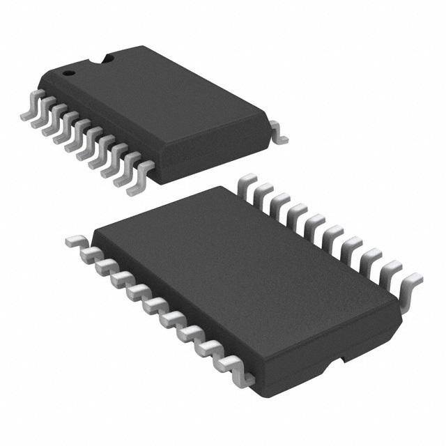
| 描述 | IC D-TYPE POS TRG SNGL 20SOIC触发器 3.3V ABT Octal D-Typ Flip-Flop W/Clear |
| 产品分类 | |
| 品牌 | Texas Instruments |
| 产品手册 | |
| 产品图片 |
|
| rohs | 符合RoHS无铅 / 符合限制有害物质指令(RoHS)规范要求 |
| 产品系列 | 逻辑集成电路,触发器,Texas Instruments SN74LVTH273DWR74LVTH |
| 数据手册 | |
| 产品型号 | SN74LVTH273DWR |
| 不同V、最大CL时的最大传播延迟 | 4.9ns @ 3.3V,50pF |
| 产品目录页面 | |
| 产品种类 | 触发器 |
| 传播延迟时间 | 3.2 ns |
| 低电平输出电流 | 64 mA |
| 元件数 | 1 |
| 其它名称 | 296-14934-1 |
| 功能 | 主复位 |
| 包装 | 剪切带 (CT) |
| 单位重量 | 500.700 mg |
| 商标 | Texas Instruments |
| 安装类型 | 表面贴装 |
| 安装风格 | SMD/SMT |
| 封装 | Reel |
| 封装/外壳 | 20-SOIC(0.295",7.50mm 宽) |
| 封装/箱体 | SOIC-20 Wide |
| 工作温度 | -40°C ~ 85°C (TA) |
| 工厂包装数量 | 2000 |
| 最大工作温度 | + 85 C |
| 最小工作温度 | - 40 C |
| 极性 | Non-Inverting |
| 标准包装 | 1 |
| 每元件位数 | 8 |
| 电压-电源 | 2.7 V ~ 3.6 V |
| 电流-输出高,低 | 32mA,64mA |
| 电流-静态 | 190µA |
| 电源电压-最大 | 3.6 V |
| 电源电压-最小 | 2.7 V |
| 电路数量 | 8 |
| 类型 | D 型 |
| 系列 | SN74LVTH273 |
| 触发器类型 | 正边沿 |
| 输入电容 | 4pF |
| 输入类型 | TTL |
| 输入线路数量 | 8 |
| 输出类型 | 非反相 |
| 输出线路数量 | 8 |
| 逻辑类型 | D-Type Flip-Flop |
| 逻辑系列 | LVT |
| 频率-时钟 | 150MHz |
| 高电平输出电流 | - 32 mA |


PDF Datasheet 数据手册内容提取
(cid:1)(cid:2)(cid:3)(cid:4)(cid:5)(cid:6)(cid:7)(cid:8)(cid:9)(cid:10)(cid:11)(cid:12) (cid:1)(cid:2)(cid:10)(cid:4)(cid:5)(cid:6)(cid:7)(cid:8)(cid:9)(cid:10)(cid:11) (cid:11)(cid:13)(cid:11)(cid:14)(cid:6) (cid:15)(cid:16)(cid:7) (cid:17)(cid:18)(cid:7)(cid:15)(cid:5) (cid:19)(cid:14)(cid:7)(cid:20)(cid:21)(cid:22) (cid:23)(cid:5)(cid:24)(cid:21)(cid:14)(cid:23)(cid:5)(cid:17)(cid:21)(cid:1) (cid:25)(cid:24)(cid:7)(cid:8) (cid:18)(cid:5)(cid:22)(cid:15)(cid:26) SCBS136M − MAY 1992 − REVISED OCTOBER 2003 (cid:1) (cid:1) Support Mixed-Mode Signal Operation Ioff Supports Partial-Power-Down-Mode (5-V Input and Output Voltages With Operation 3.3-V VCC) (cid:1) Bus Hold on Data Inputs Eliminates the (cid:1) Typical V (Output Ground Bounce) Need for External Pullup/Pulldown OLP <0.8 V at V = 3.3 V, T = 25°C Resistors CC A (cid:1) (cid:1) Support Unregulated Battery Operation Latch-Up Performance Exceeds 500 mA Per Down To 2.7 V JESD 17 (cid:1) (cid:1) Buffered Clock and Direct-Clear Inputs ESD Protection Exceeds JESD 22 (cid:1) Individual Data Input to Each Flip-Flop − 2000-V Human-Body Model (A114-A) − 200-V Machine Model (A115-A) SN54LVTH273...J PACKAGE SN54LVTH273...FK PACKAGE SN74LVTH273...DB, DW, NS, OR PW PACKAGE (TOP VIEW) (TOP VIEW) R C DQ L CQ CLR 1 20 V 11 CV 8 CC 1Q 2 19 8Q 3 2 1 20 19 1D 3 18 8D 2D 4 18 8D 2D 4 17 7D 2Q 5 17 7D 2Q 5 16 7Q 3Q 6 16 7Q 3Q 6 15 6Q 3D 7 15 6Q 3D 7 14 6D 4D 8 14 6D 9 10 11 12 13 4D 8 13 5D 4Q 9 12 5Q Q D K Q D 4 N L 5 5 GND 10 11 CLK G C description/ordering information These octal D-type flip-flops are designed specifically for low-voltage (3.3-V) V operation, but with the CC capability to provide a TTL interface to a 5-V system environment. The ’LVTH273 devices are positive-edge-triggered flip-flops with a direct-clear input. Information at the data (D) inputs meeting the setup-time requirements is transferred to the Q outputs on the positive-going edge of the clock pulse. Clock triggering occurs at a particular voltage level and is not directly related to the transition time of the positive-going pulse. When the clock (CLK) input is at either the high or low level, the D-input signal has no effect at the output. ORDERING INFORMATION ORDERABLE TOP-SIDE TA PACKAGE† PART NUMBER MARKING Tube SN74LVTH273DW SSOOIICC −− DDWW LLVVTTHH227733 Tape and reel SN74LVTH273DWR SOP − NS Tape and reel SN74LVTH273NSR LVTH273 −−4400°°CC ttoo 8855°°CC SSOP − DB Tape and reel SN74LVTH273DBR LXH273 Tube SN74LVTH273PW TTSSSSOOPP −− PPWW LLXXHH227733 Tape and reel SN74LVTH273PWR CDIP − J Tube SNJ54LVTH273J SNJ54LVTH273J −−5555°°CC ttoo 112255°°CC LCCC − FK Tube SNJ54LVTH273FK SNJ54LVTH273FK †Package drawings, standard packing quantities, thermal data, symbolization, and PCB design guidelines are available at www.ti.com/sc/package. Please be aware that an important notice concerning availability, standard warranty, and use in critical applications of TexasInstruments semiconductor products and disclaimers thereto appears at the end of this data sheet. (cid:27)(cid:2)(cid:5)(cid:22)(cid:1)(cid:1) (cid:17)(cid:7)(cid:8)(cid:22)(cid:26)(cid:25)(cid:24)(cid:1)(cid:22) (cid:2)(cid:17)(cid:7)(cid:22)(cid:19) (cid:28)(cid:29)(cid:30)(cid:31) !"#$%&’(cid:28) #"’(cid:28)((cid:30)’(cid:31) (cid:21)(cid:26)(cid:17)(cid:19)(cid:27)(cid:18)(cid:7)(cid:24)(cid:17)(cid:2) Copyright 2003, Texas Instruments Incorporated (cid:19)(cid:15)(cid:7)(cid:15) (cid:30)’)"*%((cid:28)(cid:30)"’ #$**&’(cid:28) ((cid:31) ") +$,-(cid:30)#((cid:28)(cid:30)"’ !((cid:28)&(cid:13) (cid:21)*"!$#(cid:28)(cid:31) #"’)"*% (cid:28)" (cid:31)+&#(cid:30))(cid:30)#((cid:28)(cid:30)"’(cid:31) +&* (cid:28)(cid:29)& (cid:28)&*%(cid:31) ") (cid:7)&.((cid:31) (cid:24)’(cid:31)(cid:28)*$%&’(cid:28)(cid:31) (cid:31)(cid:28)(’!(*! /(**(’(cid:28)0(cid:13) (cid:21)*"!$#(cid:28)(cid:30)"’ +*"#&(cid:31)(cid:31)(cid:30)’1 !"&(cid:31) ’"(cid:28) ’&#&(cid:31)(cid:31)(*(cid:30)-0 (cid:30)’#-$!& (cid:28)&(cid:31)(cid:28)(cid:30)’1 ") (-- +(*(%&(cid:28)&*(cid:31)(cid:13) POST OFFICE BOX 655303 • DALLAS, TEXAS 75265 1
(cid:1)(cid:2)(cid:3)(cid:4)(cid:5)(cid:6)(cid:7)(cid:8)(cid:9)(cid:10)(cid:11)(cid:12) (cid:1)(cid:2)(cid:10)(cid:4)(cid:5)(cid:6)(cid:7)(cid:8)(cid:9)(cid:10)(cid:11) (cid:11)(cid:13)(cid:11)(cid:14)(cid:6) (cid:15)(cid:16)(cid:7) (cid:17)(cid:18)(cid:7)(cid:15)(cid:5) (cid:19)(cid:14)(cid:7)(cid:20)(cid:21)(cid:22) (cid:23)(cid:5)(cid:24)(cid:21)(cid:14)(cid:23)(cid:5)(cid:17)(cid:21)(cid:1) (cid:25)(cid:24)(cid:7)(cid:8) (cid:18)(cid:5)(cid:22)(cid:15)(cid:26) SCBS136M − MAY 1992 − REVISED OCTOBER 2003 description/ordering information (continued) Active bus-hold circuitry holds unused or undriven inputs at a valid logic state. Use of pullup or pulldown resistors with the bus-hold circuitry is not recommended. These devices are fully specified for partial-power-down applications using Ioff. The Ioff circuitry disables the outputs, preventing damaging current backflow through the devices when they are powered down. FUNCTION TABLE (each flip-flop) INPUTS OOUUTTPPUUTT CLR CLK D Q L X X L H ↑ H H H ↑ L L H H or L X Q0 logic diagram (positive logic) 1D 2D 3D 4D 5D 6D 7D 8D 3 4 7 8 13 14 17 18 11 CLK CLK(I) 1D 1D 1D 1D 1D 1D 1D 1D C1 C1 C1 C1 C1 C1 C1 C1 R R R R R R R R 1 R CLR 2 5 6 9 12 15 16 19 1Q 2Q 3Q 4Q 5Q 6Q 7Q 8Q 2 POST OFFICE BOX 655303 • DALLAS, TEXAS 75265
(cid:1)(cid:2)(cid:3)(cid:4)(cid:5)(cid:6)(cid:7)(cid:8)(cid:9)(cid:10)(cid:11)(cid:12) (cid:1)(cid:2)(cid:10)(cid:4)(cid:5)(cid:6)(cid:7)(cid:8)(cid:9)(cid:10)(cid:11) (cid:11)(cid:13)(cid:11)(cid:14)(cid:6) (cid:15)(cid:16)(cid:7) (cid:17)(cid:18)(cid:7)(cid:15)(cid:5) (cid:19)(cid:14)(cid:7)(cid:20)(cid:21)(cid:22) (cid:23)(cid:5)(cid:24)(cid:21)(cid:14)(cid:23)(cid:5)(cid:17)(cid:21)(cid:1) (cid:25)(cid:24)(cid:7)(cid:8) (cid:18)(cid:5)(cid:22)(cid:15)(cid:26) SCBS136M − MAY 1992 − REVISED OCTOBER 2003 absolute maximum ratings over operating free-air temperature range (unless otherwise noted)† Supply voltage range, V . . . . . . . . . . . . . . . . . . . . . . . . . . . . . . . . . . . . . . . . . . . . . . . . . . . . . . . . . −0.5 V to 4.6 V CC Input voltage range, V (see Note 1) . . . . . . . . . . . . . . . . . . . . . . . . . . . . . . . . . . . . . . . . . . . . . . . . . . −0.5 V to 7 V I Voltage range applied to any output in the power-off state, VO (see Note 1) . . . . . . . . . . . . . . . . −0.5 V to 7 V Voltage range applied to any output in the high state, VO (see Note 1) . . . . . . . . . . . . . −0.5 V to VCC + 0.5 V Current into any output in the low state, I : SN54LVTH273 . . . . . . . . . . . . . . . . . . . . . . . . . . . . . . . . . . . 96 mA O SN74LVTH273 . . . . . . . . . . . . . . . . . . . . . . . . . . . . . . . . . . 128 mA Current into any output in the high state, IO (see Note 2): SN54LVTH273 . . . . . . . . . . . . . . . . . . . . . . . 48 mA SN74LVTH273 . . . . . . . . . . . . . . . . . . . . . . . 64 mA Input clamp current, IIK (VI < 0) . . . . . . . . . . . . . . . . . . . . . . . . . . . . . . . . . . . . . . . . . . . . . . . . . . . . . . . . . . . −50 mA Output clamp current, IOK (VO < 0) . . . . . . . . . . . . . . . . . . . . . . . . . . . . . . . . . . . . . . . . . . . . . . . . . . . . . . . . −50 mA Package thermal impedance, θJA (see Note 3): DB package . . . . . . . . . . . . . . . . . . . . . . . . . . . . . . . . . 70°C/W DW package . . . . . . . . . . . . . . . . . . . . . . . . . . . . . . . . . 58°C/W NS package . . . . . . . . . . . . . . . . . . . . . . . . . . . . . . . . . 60°C/W PW package . . . . . . . . . . . . . . . . . . . . . . . . . . . . . . . . . 83°C/W Storage temperature range, T . . . . . . . . . . . . . . . . . . . . . . . . . . . . . . . . . . . . . . . . . . . . . . . . . . . −65°C to 150°C stg †Stresses beyond those listed under “absolute maximum ratings” may cause permanent damage to the device. These are stress ratings only, and functional operation of the device at these or any other conditions beyond those indicated under “recommended operating conditions” is not implied. Exposure to absolute-maximum-rated conditions for extended periods may affect device reliability. NOTES: 1. The input and output negative-voltage ratings may be exceeded if the input and output clamp-current ratings are observed. 2. This current flows only when the output is in the high state and VO > VCC. 3. The package thermal impedance is calculated in accordance with JESD 51-7. recommended operating conditions (see Note 4) SN54LVTH273 SN74LVTH273 UUNNIITT MIN MAX MIN MAX VCC Supply voltage 2.7 3.6 2.7 3.6 V VIH High-level input voltage 2 2 V VIL Low-level input voltage 0.8 0.8 V VI Input voltage 5.5 5.5 V IOH High-level output current −24 −32 mA IOL Low-level output current 48 64 mA ∆t/∆v Input transition rise or fall rate 10 10 ns/V TA Operating free-air temperature −55 125 −40 85 °C NOTE 4: All unused control inputs of the device must be held at VCC or GND to ensure proper device operation. Refer to the TI application report, Implications of Slow or Floating CMOS Inputs, literature number SCBA004. (cid:21)(cid:26)(cid:17)(cid:19)(cid:27)(cid:18)(cid:7) (cid:21)(cid:26)(cid:22)(cid:6)(cid:24)(cid:22)(cid:25) (cid:30)’)"*%((cid:28)(cid:30)"’ #"’#&*’(cid:31) +*"!$#(cid:28)(cid:31) (cid:30)’ (cid:28)(cid:29)& )"*%((cid:28)(cid:30)2& "* !&(cid:31)(cid:30)1’ +(cid:29)((cid:31)& ") !&2&-"+%&’(cid:28)(cid:13) (cid:18)(cid:29)(*(#(cid:28)&*(cid:30)(cid:31)(cid:28)(cid:30)# !((cid:28)( (’! "(cid:28)(cid:29)&* (cid:31)+&#(cid:30))(cid:30)#((cid:28)(cid:30)"’(cid:31) (*& !&(cid:31)(cid:30)1’ 1"(-(cid:31)(cid:13) (cid:7)&.((cid:31) (cid:24)’(cid:31)(cid:28)*$%&’(cid:28)(cid:31) *&(cid:31)&*2&(cid:31) (cid:28)(cid:29)& *(cid:30)1(cid:29)(cid:28) (cid:28)" #(cid:29)(’1& "* !(cid:30)(cid:31)#"’(cid:28)(cid:30)’$& (cid:28)(cid:29)&(cid:31)& +*"!$#(cid:28)(cid:31) /(cid:30)(cid:28)(cid:29)"$(cid:28) ’"(cid:28)(cid:30)#&(cid:13) POST OFFICE BOX 655303 • DALLAS, TEXAS 75265 3
(cid:1)(cid:2)(cid:3)(cid:4)(cid:5)(cid:6)(cid:7)(cid:8)(cid:9)(cid:10)(cid:11)(cid:12) (cid:1)(cid:2)(cid:10)(cid:4)(cid:5)(cid:6)(cid:7)(cid:8)(cid:9)(cid:10)(cid:11) (cid:11)(cid:13)(cid:11)(cid:14)(cid:6) (cid:15)(cid:16)(cid:7) (cid:17)(cid:18)(cid:7)(cid:15)(cid:5) (cid:19)(cid:14)(cid:7)(cid:20)(cid:21)(cid:22) (cid:23)(cid:5)(cid:24)(cid:21)(cid:14)(cid:23)(cid:5)(cid:17)(cid:21)(cid:1) (cid:25)(cid:24)(cid:7)(cid:8) (cid:18)(cid:5)(cid:22)(cid:15)(cid:26) SCBS136M − MAY 1992 − REVISED OCTOBER 2003 electrical characteristics over recommended operating free-air temperature range (unless otherwise noted) SN54LVTH273 SN74LVTH273 PPAARRAAMMEETTEERR TTEESSTT CCOONNDDIITTIIOONNSS UUNNIITT MIN TYP† MAX MIN TYP† MAX VIK VCC = 2.7 V, II = −18 mA −1.2 −1.2 V VCC = 2.7 V to 3.6 V, IOH = −100 µA VCC−0.2 VCC−0.2 VCC = 2.7 V, IOH = −8 mA 2.4 2.4 VVOOHH VV IOH = −24 mA 2 VVCCCC == 33 VV IOH = −32 mA 2 IOL = 100 µA 0.2 0.2 VVCCCC == 22..77 VV IOL = 24 mA 0.5 0.5 IOL = 16 mA 0.4 0.4 VVOOLL VV IOL = 32 mA 0.5 0.5 VVCCCC == 33 VV IOL = 48 mA 0.55 IOL = 64 mA 0.55 VCC = 0 or 3.6 V, VI = 5.5 V 10 10 Control inputs VCC = 3.6 V, VI = VCC or GND ±1 ±1 IIII µAA VI = VCC 1 1 DDaattaa iinnppuuttss VVCCCC == 33..66 VV VI = 0 −5 −5 Ioff VCC = 0, VI or VO = 0 to 4.5 V ±100 µA VI = 0.8 V 75 75 VVCCCC == 33 VV IIII((hhoolldd)) DDaattaa iinnppuuttss VI = 2 V −75 −75 µµAA 500 VCC = 3.6 V‡, VI = 0 to 3.6 V −750 VVCCCC == 33..66 VV,, IIOO == 00,, Outputs high 0.19 0.19 IICCCC VI = VCC or GND Outputs low 5 5 mmAA ∆ICC§ VOCthCe r= i n3p Vut sto a 3t .V6C VC, O onr eG iNnpDut at VCC − 0.6 V, 0.2 0.2 mA Ci VI = 3 V or 0 4 4 pF †All typical values are at VCC = 3.3 V, TA = 25°C. ‡This is the bus-hold maximum dynamic current. It is the minimum overdrive current required to switch the input from one state to another. §This is the increase in supply current for each input that is at the specified TTL voltage level, rather than VCC or GND. timing requirements over recommended operating free-air temperature range (unless otherwise noted) (see Figure 1) SN54LVTH273 SN74LVTH273 VCC = 3.3 V VCC = 3.3 V ±0.3 V VCC = 2.7 V ± 0.3 V VCC = 2.7 V UNIT MIN MAX MIN MAX MIN MAX MIN MAX fclock Clock frequency 150 150 MHz tw Pulse duration 3.3 3.3 3.3 3.3 ns Data high or low before CLK↑ 2.3 2.7 2.3 2.7 ttssuu SSeettuupp ttiimmee CLR high before CLK↑ 2.3 2.7 2.3 2.7 nnss th Hold time, data high or low after CLK↑ 0 0 0 0 ns (cid:21)(cid:26)(cid:17)(cid:19)(cid:27)(cid:18)(cid:7) (cid:21)(cid:26)(cid:22)(cid:6)(cid:24)(cid:22)(cid:25) (cid:30)’)"*%((cid:28)(cid:30)"’ #"’#&*’(cid:31) +*"!$#(cid:28)(cid:31) (cid:30)’ (cid:28)(cid:29)& )"*%((cid:28)(cid:30)2& "* !&(cid:31)(cid:30)1’ +(cid:29)((cid:31)& ") !&2&-"+%&’(cid:28)(cid:13) (cid:18)(cid:29)(*(#(cid:28)&*(cid:30)(cid:31)(cid:28)(cid:30)# !((cid:28)( (’! "(cid:28)(cid:29)&* (cid:31)+&#(cid:30))(cid:30)#((cid:28)(cid:30)"’(cid:31) (*& !&(cid:31)(cid:30)1’ 1"(-(cid:31)(cid:13) (cid:7)&.((cid:31) (cid:24)’(cid:31)(cid:28)*$%&’(cid:28)(cid:31) *&(cid:31)&*2&(cid:31) (cid:28)(cid:29)& *(cid:30)1(cid:29)(cid:28) (cid:28)" #(cid:29)(’1& "* !(cid:30)(cid:31)#"’(cid:28)(cid:30)’$& (cid:28)(cid:29)&(cid:31)& +*"!$#(cid:28)(cid:31) /(cid:30)(cid:28)(cid:29)"$(cid:28) ’"(cid:28)(cid:30)#&(cid:13) 4 POST OFFICE BOX 655303 • DALLAS, TEXAS 75265
(cid:1)(cid:2)(cid:3)(cid:4)(cid:5)(cid:6)(cid:7)(cid:8)(cid:9)(cid:10)(cid:11)(cid:12) (cid:1)(cid:2)(cid:10)(cid:4)(cid:5)(cid:6)(cid:7)(cid:8)(cid:9)(cid:10)(cid:11) (cid:11)(cid:13)(cid:11)(cid:14)(cid:6) (cid:15)(cid:16)(cid:7) (cid:17)(cid:18)(cid:7)(cid:15)(cid:5) (cid:19)(cid:14)(cid:7)(cid:20)(cid:21)(cid:22) (cid:23)(cid:5)(cid:24)(cid:21)(cid:14)(cid:23)(cid:5)(cid:17)(cid:21)(cid:1) (cid:25)(cid:24)(cid:7)(cid:8) (cid:18)(cid:5)(cid:22)(cid:15)(cid:26) SCBS136M − MAY 1992 − REVISED OCTOBER 2003 switching characteristics over recommended operating free-air temperature range, C = 50 pF L (unless otherwise noted) (see Figure 1) SN54LVTH273 SN74LVTH273 FROM TO VCC = 3.3 V VCC = 3.3 V PARAMETER ((IINNPPUUTT)) ((OOUUTTPPUUTT)) ± 0.3 V VCC = 2.7 V ± 0.3 V VCC = 2.7 V UNIT MIN MAX MIN MAX MIN TYP† MAX MIN MAX fmax 150 150 MHz tPLH 1.6 5 5.6 1.7 3.2 4.9 5.5 CCLLKK AAnnyy QQ nnss tPHL 1.8 4.9 5.2 1.9 3.2 4.8 5.1 tPHL CLR Any Q 1.5 4.4 4.8 1.6 2.7 4.3 4.7 ns †All typical values are at VCC = 3.3 V, TA = 25°C. (cid:21)(cid:26)(cid:17)(cid:19)(cid:27)(cid:18)(cid:7) (cid:21)(cid:26)(cid:22)(cid:6)(cid:24)(cid:22)(cid:25) (cid:30)’)"*%((cid:28)(cid:30)"’ #"’#&*’(cid:31) +*"!$#(cid:28)(cid:31) (cid:30)’ (cid:28)(cid:29)& )"*%((cid:28)(cid:30)2& "* !&(cid:31)(cid:30)1’ +(cid:29)((cid:31)& ") !&2&-"+%&’(cid:28)(cid:13) (cid:18)(cid:29)(*(#(cid:28)&*(cid:30)(cid:31)(cid:28)(cid:30)# !((cid:28)( (’! "(cid:28)(cid:29)&* (cid:31)+&#(cid:30))(cid:30)#((cid:28)(cid:30)"’(cid:31) (*& !&(cid:31)(cid:30)1’ 1"(-(cid:31)(cid:13) (cid:7)&.((cid:31) (cid:24)’(cid:31)(cid:28)*$%&’(cid:28)(cid:31) *&(cid:31)&*2&(cid:31) (cid:28)(cid:29)& *(cid:30)1(cid:29)(cid:28) (cid:28)" #(cid:29)(’1& "* !(cid:30)(cid:31)#"’(cid:28)(cid:30)’$& (cid:28)(cid:29)&(cid:31)& +*"!$#(cid:28)(cid:31) /(cid:30)(cid:28)(cid:29)"$(cid:28) ’"(cid:28)(cid:30)#&(cid:13) POST OFFICE BOX 655303 • DALLAS, TEXAS 75265 5
(cid:1)(cid:2)(cid:3)(cid:4)(cid:5)(cid:6)(cid:7)(cid:8)(cid:9)(cid:10)(cid:11)(cid:12) (cid:1)(cid:2)(cid:10)(cid:4)(cid:5)(cid:6)(cid:7)(cid:8)(cid:9)(cid:10)(cid:11) (cid:11)(cid:13)(cid:11)(cid:14)(cid:6) (cid:15)(cid:16)(cid:7) (cid:17)(cid:18)(cid:7)(cid:15)(cid:5) (cid:19)(cid:14)(cid:7)(cid:20)(cid:21)(cid:22) (cid:23)(cid:5)(cid:24)(cid:21)(cid:14)(cid:23)(cid:5)(cid:17)(cid:21)(cid:1) (cid:25)(cid:24)(cid:7)(cid:8) (cid:18)(cid:5)(cid:22)(cid:15)(cid:26) SCBS136M − MAY 1992 − REVISED OCTOBER 2003 PARAMETER MEASUREMENT INFORMATION 6 V 500 Ω S1 Open TEST S1 From Output Under Test GND tPLH/tPHL Open CL = 50 pF tPLZ/tPZL 6 V (see Note A) 500 Ω tPHZ/tPZH GND 2.7 V LOAD CIRCUIT Timing Input 1.5 V 0 V tw tsu th 2.7 V 2.7 V Input 1.5 V 1.5 V Data Input 1.5 V 1.5 V 0 V 0 V VOLTAGE WAVEFORMS VOLTAGE WAVEFORMS PULSE DURATION SETUP AND HOLD TIMES 2.7 V 2.7 V Output Input 1.5 V 1.5 V 1.5 V 1.5 V Control 0 V 0 V tPLH tPHL tPZL tPLZ VOH Output 3 V Output 1.5 V 1.5 V WavSe1f oart m6 V1 1.5 V VOL + 0.3 V VOL VOL (see Note B) tPHL tPLH tPZH tPHZ Output VOH VOH Output 1.5 V 1.5 V WSa1v eafto GrmN D2 1.5 V VOH − 0.3 V VOL (see Note B) ≈0 V VOLTAGE WAVEFORMS VOLTAGE WAVEFORMS PROPAGATION DELAY TIMES ENABLE AND DISABLE TIMES INVERTING AND NONINVERTING OUTPUTS LOW- AND HIGH-LEVEL ENABLING NOTES: A. CL includes probe and jig capacitance. B. Waveform 1 is for an output with internal conditions such that the output is low except when disabled by the output control. Waveform2 is for an output with internal conditions such that the output is high except when disabled by the output control. C. All input pulses are supplied by generators having the following characteristics: PRR ≤ 10 MHz, ZO = 50 Ω, tr ≤ 2.5 ns, tf≤ 2.5 ns. D. The outputs are measured one at a time with one transition per measurement. Figure 1. Load Circuit and Voltage Waveforms 6 POST OFFICE BOX 655303 • DALLAS, TEXAS 75265
PACKAGE OPTION ADDENDUM www.ti.com 6-Feb-2020 PACKAGING INFORMATION Orderable Device Status Package Type Package Pins Package Eco Plan Lead/Ball Finish MSL Peak Temp Op Temp (°C) Device Marking Samples (1) Drawing Qty (2) (6) (3) (4/5) SN74LVTH273DBR ACTIVE SSOP DB 20 2000 Green (RoHS NIPDAU Level-1-260C-UNLIM -40 to 85 LXH273 & no Sb/Br) SN74LVTH273DW ACTIVE SOIC DW 20 25 Green (RoHS NIPDAU Level-1-260C-UNLIM -40 to 85 LVTH273 & no Sb/Br) SN74LVTH273DWR ACTIVE SOIC DW 20 2000 Green (RoHS NIPDAU Level-1-260C-UNLIM -40 to 85 LVTH273 & no Sb/Br) SN74LVTH273DWRE4 ACTIVE SOIC DW 20 2000 Green (RoHS NIPDAU Level-1-260C-UNLIM -40 to 85 LVTH273 & no Sb/Br) SN74LVTH273DWRG4 ACTIVE SOIC DW 20 2000 Green (RoHS NIPDAU Level-1-260C-UNLIM -40 to 85 LVTH273 & no Sb/Br) SN74LVTH273NSR ACTIVE SO NS 20 2000 Green (RoHS NIPDAU Level-1-260C-UNLIM -40 to 85 LVTH273 & no Sb/Br) SN74LVTH273PW ACTIVE TSSOP PW 20 70 Green (RoHS NIPDAU Level-1-260C-UNLIM -40 to 85 LXH273 & no Sb/Br) SN74LVTH273PWR ACTIVE TSSOP PW 20 2000 Green (RoHS NIPDAU | SN Level-1-260C-UNLIM -40 to 85 LXH273 & no Sb/Br) SN74LVTH273PWRG4 ACTIVE TSSOP PW 20 2000 Green (RoHS NIPDAU Level-1-260C-UNLIM -40 to 85 LXH273 & no Sb/Br) (1) The marketing status values are defined as follows: ACTIVE: Product device recommended for new designs. LIFEBUY: TI has announced that the device will be discontinued, and a lifetime-buy period is in effect. NRND: Not recommended for new designs. Device is in production to support existing customers, but TI does not recommend using this part in a new design. PREVIEW: Device has been announced but is not in production. Samples may or may not be available. OBSOLETE: TI has discontinued the production of the device. (2) RoHS: TI defines "RoHS" to mean semiconductor products that are compliant with the current EU RoHS requirements for all 10 RoHS substances, including the requirement that RoHS substance do not exceed 0.1% by weight in homogeneous materials. Where designed to be soldered at high temperatures, "RoHS" products are suitable for use in specified lead-free processes. TI may reference these types of products as "Pb-Free". RoHS Exempt: TI defines "RoHS Exempt" to mean products that contain lead but are compliant with EU RoHS pursuant to a specific EU RoHS exemption. Green: TI defines "Green" to mean the content of Chlorine (Cl) and Bromine (Br) based flame retardants meet JS709B low halogen requirements of <=1000ppm threshold. Antimony trioxide based flame retardants must also meet the <=1000ppm threshold requirement. (3) MSL, Peak Temp. - The Moisture Sensitivity Level rating according to the JEDEC industry standard classifications, and peak solder temperature. Addendum-Page 1
PACKAGE OPTION ADDENDUM www.ti.com 6-Feb-2020 (4) There may be additional marking, which relates to the logo, the lot trace code information, or the environmental category on the device. (5) Multiple Device Markings will be inside parentheses. Only one Device Marking contained in parentheses and separated by a "~" will appear on a device. If a line is indented then it is a continuation of the previous line and the two combined represent the entire Device Marking for that device. (6) Lead/Ball Finish - Orderable Devices may have multiple material finish options. Finish options are separated by a vertical ruled line. Lead/Ball Finish values may wrap to two lines if the finish value exceeds the maximum column width. Important Information and Disclaimer:The information provided on this page represents TI's knowledge and belief as of the date that it is provided. TI bases its knowledge and belief on information provided by third parties, and makes no representation or warranty as to the accuracy of such information. Efforts are underway to better integrate information from third parties. TI has taken and continues to take reasonable steps to provide representative and accurate information but may not have conducted destructive testing or chemical analysis on incoming materials and chemicals. TI and TI suppliers consider certain information to be proprietary, and thus CAS numbers and other limited information may not be available for release. In no event shall TI's liability arising out of such information exceed the total purchase price of the TI part(s) at issue in this document sold by TI to Customer on an annual basis. OTHER QUALIFIED VERSIONS OF SN74LVTH273 : •Enhanced Product: SN74LVTH273-EP NOTE: Qualified Version Definitions: •Enhanced Product - Supports Defense, Aerospace and Medical Applications Addendum-Page 2
PACKAGE MATERIALS INFORMATION www.ti.com 2-Oct-2019 TAPE AND REEL INFORMATION *Alldimensionsarenominal Device Package Package Pins SPQ Reel Reel A0 B0 K0 P1 W Pin1 Type Drawing Diameter Width (mm) (mm) (mm) (mm) (mm) Quadrant (mm) W1(mm) SN74LVTH273DBR SSOP DB 20 2000 330.0 16.4 8.2 7.5 2.5 12.0 16.0 Q1 SN74LVTH273DWR SOIC DW 20 2000 330.0 24.4 10.8 13.3 2.7 12.0 24.0 Q1 SN74LVTH273NSR SO NS 20 2000 330.0 24.4 8.4 13.0 2.5 12.0 24.0 Q1 SN74LVTH273PWR TSSOP PW 20 2000 330.0 16.4 6.95 7.0 1.4 8.0 16.0 Q1 SN74LVTH273PWRG4 TSSOP PW 20 2000 330.0 16.4 6.95 7.0 1.4 8.0 16.0 Q1 PackMaterials-Page1
PACKAGE MATERIALS INFORMATION www.ti.com 2-Oct-2019 *Alldimensionsarenominal Device PackageType PackageDrawing Pins SPQ Length(mm) Width(mm) Height(mm) SN74LVTH273DBR SSOP DB 20 2000 367.0 367.0 38.0 SN74LVTH273DWR SOIC DW 20 2000 367.0 367.0 45.0 SN74LVTH273NSR SO NS 20 2000 367.0 367.0 45.0 SN74LVTH273PWR TSSOP PW 20 2000 367.0 367.0 38.0 SN74LVTH273PWRG4 TSSOP PW 20 2000 367.0 367.0 38.0 PackMaterials-Page2
None
None
PACKAGE OUTLINE DW0020A SOIC - 2.65 mm max height SCALE 1.200 SOIC C 10.63 SEATING PLANE TYP 9.97 A PIN 1 ID 0.1 C AREA 18X 1.27 20 1 13.0 2X 12.6 11.43 NOTE 3 10 11 0.51 20X 7.6 0.31 2.65 MAX B 7.4 0.25 C A B NOTE 4 0.33 TYP 0.10 0.25 SEE DETAIL A GAGE PLANE 0.3 1.27 0 - 8 0.1 0.40 DETAIL A TYPICAL 4220724/A 05/2016 NOTES: 1. All linear dimensions are in millimeters. Dimensions in parenthesis are for reference only. Dimensioning and tolerancing per ASME Y14.5M. 2. This drawing is subject to change without notice. 3. This dimension does not include mold flash, protrusions, or gate burrs. Mold flash, protrusions, or gate burrs shall not exceed 0.15 mm per side. 4. This dimension does not include interlead flash. Interlead flash shall not exceed 0.43 mm per side. 5. Reference JEDEC registration MS-013. www.ti.com
EXAMPLE BOARD LAYOUT DW0020A SOIC - 2.65 mm max height SOIC 20X (2) SYMM 1 20 20X (0.6) 18X (1.27) SYMM (R0.05) TYP 10 11 (9.3) LAND PATTERN EXAMPLE SCALE:6X SOOPLEDNEINRG MASK METAL MSOELTDAEL RU NMDAESRK SOOPLEDNEINRG MASK 0.07 MAX 0.07 MIN ALL AROUND ALL AROUND NON SOLDER MASK SOLDER MASK DEFINED DEFINED SOLDER MASK DETAILS 4220724/A 05/2016 NOTES: (continued) 6. Publication IPC-7351 may have alternate designs. 7. Solder mask tolerances between and around signal pads can vary based on board fabrication site. www.ti.com
EXAMPLE STENCIL DESIGN DW0020A SOIC - 2.65 mm max height SOIC 20X (2) SYMM 1 20 20X (0.6) 18X (1.27) SYMM 10 11 (9.3) SOLDER PASTE EXAMPLE BASED ON 0.125 mm THICK STENCIL SCALE:6X 4220724/A 05/2016 NOTES: (continued) 8. Laser cutting apertures with trapezoidal walls and rounded corners may offer better paste release. IPC-7525 may have alternate design recommendations. 9. Board assembly site may have different recommendations for stencil design. www.ti.com
PACKAGE OUTLINE DB0020A SSOP - 2 mm max height SCALE 2.000 SMALL OUTLINE PACKAGE C 8.2 TYP 7.4 A 0.1 C PIN 1 INDEX AREA SEATING PLANE 18X 0.65 20 1 2X 7.5 5.85 6.9 NOTE 3 10 11 0.38 20X 0.22 5.6 B 0.1 C A B 5.0 NOTE 4 2 MAX (0.15) TYP 0.25 SEE DETAIL A GAGE PLANE 0 -8 0.95 0.05 MIN 0.55 DETA 15AIL A TYPICAL 4214851/B 08/2019 NOTES: 1. All linear dimensions are in millimeters. Any dimensions in parenthesis are for reference only. Dimensioning and tolerancing per ASME Y14.5M. 2. This drawing is subject to change without notice. 3. This dimension does not include mold flash, protrusions, or gate burrs. Mold flash, protrusions, or gate burrs shall not exceed 0.15 mm per side. 4. This dimension does not include interlead flash. Interlead flash shall not exceed 0.25 mm per side. 5. Reference JEDEC registration MO-150. www.ti.com
EXAMPLE BOARD LAYOUT DB0020A SSOP - 2 mm max height SMALL OUTLINE PACKAGE 20X (1.85) SYMM (R0.05) TYP 1 20X (0.45) 20 SYMM 18X (0.65) 10 11 (7) LAND PATTERN EXAMPLE EXPOSED METAL SHOWN SCALE: 10X SOLDER MASK METAL METAL UNDER SOLDER MASK OPENING SOLDER MASK OPENING EXPOSED METAL EXPOSED METAL 0.07 MAX 0.07 MIN ALL AROUND ALL AROUND NON-SOLDER MASK SOLDER MASK DEFINED DEFINED (PREFERRED) SOLDE15.000 R MASK DETAILS 4214851/B 08/2019 NOTES: (continued) 6. Publication IPC-7351 may have alternate designs. 7. Solder mask tolerances between and around signal pads can vary based on board fabrication site. www.ti.com
EXAMPLE STENCIL DESIGN DB0020A SSOP - 2 mm max height SMALL OUTLINE PACKAGE 20X (1.85) SYMM (R0.05) TYP 1 20X (0.45) 20 SYMM 18X (0.65) 10 11 (7) SOLDER PASTE EXAMPLE BASED ON 0.125 mm THICK STENCIL SCALE: 10X 4214851/B 08/2019 NOTES: (continued) 8. Laser cutting apertures with trapezoidal walls and rounded corners may offer better paste release. IPC-7525 may have alternate design recommendations. 9. Board assembly site may have different recommendations for stencil design. www.ti.com
None
IMPORTANTNOTICEANDDISCLAIMER TI PROVIDES TECHNICAL AND RELIABILITY DATA (INCLUDING DATASHEETS), DESIGN RESOURCES (INCLUDING REFERENCE DESIGNS), APPLICATION OR OTHER DESIGN ADVICE, WEB TOOLS, SAFETY INFORMATION, AND OTHER RESOURCES “AS IS” AND WITH ALL FAULTS, AND DISCLAIMS ALL WARRANTIES, EXPRESS AND IMPLIED, INCLUDING WITHOUT LIMITATION ANY IMPLIED WARRANTIES OF MERCHANTABILITY, FITNESS FOR A PARTICULAR PURPOSE OR NON-INFRINGEMENT OF THIRD PARTY INTELLECTUAL PROPERTY RIGHTS. These resources are intended for skilled developers designing with TI products. You are solely responsible for (1) selecting the appropriate TI products for your application, (2) designing, validating and testing your application, and (3) ensuring your application meets applicable standards, and any other safety, security, or other requirements. These resources are subject to change without notice. TI grants you permission to use these resources only for development of an application that uses the TI products described in the resource. Other reproduction and display of these resources is prohibited. No license is granted to any other TI intellectual property right or to any third party intellectual property right. TI disclaims responsibility for, and you will fully indemnify TI and its representatives against, any claims, damages, costs, losses, and liabilities arising out of your use of these resources. TI’s products are provided subject to TI’s Terms of Sale (www.ti.com/legal/termsofsale.html) or other applicable terms available either on ti.com or provided in conjunction with such TI products. TI’s provision of these resources does not expand or otherwise alter TI’s applicable warranties or warranty disclaimers for TI products. Mailing Address: Texas Instruments, Post Office Box 655303, Dallas, Texas 75265 Copyright © 2020, Texas Instruments Incorporated