ICGOO在线商城 > 集成电路(IC) > 逻辑 - 缓冲器,驱动器,接收器,收发器 > SN74LVT240ANSR

 Datasheet下载
- 型号: SN74LVT240ANSR
- 制造商: Texas Instruments
- 库位|库存: xxxx|xxxx
- 要求:
| 数量阶梯 | 香港交货 | 国内含税 |
| +xxxx | $xxxx | ¥xxxx |
查看当月历史价格
查看今年历史价格
SN74LVT240ANSR产品简介:
ICGOO电子元器件商城为您提供SN74LVT240ANSR由Texas Instruments设计生产,在icgoo商城现货销售,并且可以通过原厂、代理商等渠道进行代购。 SN74LVT240ANSR价格参考。Texas InstrumentsSN74LVT240ANSR封装/规格:逻辑 - 缓冲器,驱动器,接收器,收发器, Buffer, Inverting 2 Element 4 Bit per Element 3-State Output 20-SO。您可以下载SN74LVT240ANSR参考资料、Datasheet数据手册功能说明书,资料中有SN74LVT240ANSR 详细功能的应用电路图电压和使用方法及教程。
SN74LVT240ANSR 是由 Texas Instruments(德州仪器)生产的一款逻辑器件,属于缓冲器/驱动器/接收器/收发器类别。以下是该型号的一些典型应用场景:

 1. 信号缓冲与驱动
   - SN74LVT240ANSR 提供了 8 位的三态输出缓冲器功能,适用于需要增强信号驱动能力的场景。例如,在多负载系统中,它可以帮助将弱信号转换为更强的信号,以驱动更多的负载设备。
   - 常见应用包括微处理器、FPGA 或 ASIC 的接口扩展,用于增强输出信号的驱动能力。

 2. 总线管理
   - 该芯片支持三态输出,因此非常适合用于多主设备共享总线的场景。通过控制使能引脚(G 和 /G),可以实现对总线的动态访问管理。
   - 典型应用包括地址总线或数据总线的切换和隔离,确保多个设备能够安全地共享同一总线。

 3. 电平转换
   - SN74LVT240ANSR 工作在低电压范围(1.65V 至 3.6V),适合用于不同电压域之间的信号转换。例如,在 3.3V 系统与 5V 系统之间进行通信时,它可以作为中间桥梁,确保信号的兼容性。

 4. 工业自动化
   - 在工业控制系统中,该芯片可用于信号的隔离与放大,例如 PLC(可编程逻辑控制器)中的输入输出模块设计。
   - 它还可以用于传感器信号的处理与传输,尤其是在需要高稳定性和抗干扰能力的环境中。

 5. 通信接口
   - 该芯片适用于低功耗、高速数据传输的应用场景,例如 UART、SPI 或 I2C 接口的信号增强与保护。
   - 在长距离通信中,它可以用来提高信号质量,减少噪声影响。

 6. 消费电子
   - 在消费电子产品中,SN74LVT240ANSR 可用于音频、视频或其他外设接口的设计。例如,电视、显示器或音响系统的信号处理部分可能需要用到该芯片来增强信号完整性。

 7. 汽车电子
   - 在汽车电子领域,该芯片可用于车内网络通信(如 CAN 总线或 LIN 总线)的辅助信号处理,或者用于仪表盘、娱乐系统等模块间的信号传输。

 总结
SN74LVT240ANSR 的主要应用场景集中在需要信号缓冲、驱动增强、总线管理以及电平转换的场合。其低功耗、高速度和高可靠性特点使其广泛应用于工业、通信、消费电子及汽车电子等领域。
| 参数 | 数值 |
| 产品目录 | 集成电路 (IC) |
| 描述 | IC BUFF/DVR 3ST OCTAL 20SO |
| 产品分类 | |
| 品牌 | Texas Instruments |
| 数据手册 | |
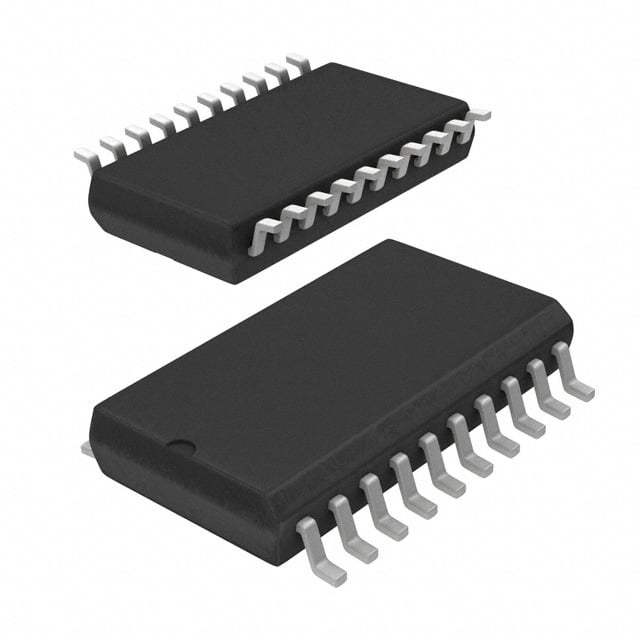
| 产品图片 |
|
| 产品型号 | SN74LVT240ANSR |
| rohs | 无铅 / 符合限制有害物质指令(RoHS)规范要求 |
| 产品系列 | 74LVT |
| 供应商器件封装 | 20-SO |
| 元件数 | 2 |
| 其它名称 | 296-28728-1 |
| 包装 | 剪切带 (CT) |
| 安装类型 | 表面贴装 |
| 封装/外壳 | 20-SOIC(0.209",5.30mm 宽) |
| 工作温度 | -40°C ~ 85°C |
| 标准包装 | 1 |
| 每元件位数 | 4 |
| 电压-电源 | 2.7 V ~ 3.6 V |
| 电流-输出高,低 | 32mA,64mA |
| 逻辑类型 | 缓冲器/线路驱动器, 反相 |


PDF Datasheet 数据手册内容提取
(cid:1)(cid:2)(cid:3)(cid:4)(cid:5)(cid:6)(cid:7)(cid:8)(cid:4)(cid:9)(cid:10) (cid:11)(cid:12)(cid:11)(cid:13)(cid:6) (cid:10)(cid:14)(cid:7) (cid:15)(cid:16)(cid:7)(cid:10)(cid:5) (cid:14)(cid:17)(cid:18)(cid:18)(cid:19)(cid:20)(cid:21)(cid:22)(cid:20)(cid:23)(cid:6)(cid:19)(cid:20) (cid:24)(cid:23)(cid:7)(cid:25) (cid:11)(cid:13)(cid:1)(cid:7)(cid:10)(cid:7)(cid:19) (cid:15)(cid:17)(cid:7)(cid:26)(cid:17)(cid:7)(cid:1) SCBS134K − SEPTEMBER 1992 − REVISED JANUARY 2004 (cid:1) Supports Mixed-Mode Signal Operation DB, DGV, DW, NS, OR PW PACKAGE (5-V Input and Output Voltages With 3.3-V (TOP VIEW) V ) CC (cid:1) 1OE 1 20 VCC Supports Unregulated Battery Operation 1A1 2 19 2OE Down To 2.7 V 2Y4 3 18 1Y1 (cid:1) Typical VOLP (Output Ground Bounce) 1A2 4 17 2A4 <0.8 V at V = 3.3 V, T = 25°C CC A 2Y3 5 16 1Y2 (cid:1) Ioff and Power-Up 3-State Support Hot 1A3 6 15 2A3 Insertion 2Y2 7 14 1Y3 (cid:1) Latch-Up Performance Exceeds 100 mA Per 1A4 8 13 2A2 JESD 78, Class II 2Y1 9 12 1Y4 (cid:1) GND 10 11 2A1 ESD Protection Exceeds JESD 22 − 2000-V Human-Body Model (A114-A) − 200-V Machine Model (A115-A) − 1000-V Charged-Device Model (C101) description/ordering information This octal buffer and line driver is designed specifically for low-voltage (3.3-V) V operation, but with the CC capability to provide a TTL interface to a 5-V system environment. The SN74LVT240A is organized as two 4-bit buffer/line drivers with separate output-enable (OE) inputs. When OE is low, the device passes data from the A inputs to the Y outputs. When OE is high, the outputs are in the high-impedance state. When V is between 0 and 1.5 V, the device is in the high-impedance state during power up or power down. CC However, to ensure the high-impedance state above 1.5 V, OE should be tied to V through a pullup resistor; CC the minimum value of the resistor is determined by the current-sinking capability of the driver. This device is fully specified for hot-insertion applications using I and power-up 3-state. The I circuitry off off disables the outputs, preventing damaging current backflow through the device when it is powered down. The power-up 3-state circuitry places the outputs in the high-impedance state during power up and power down, which prevents driver conflict. ORDERING INFORMATION ORDERABLE TOP-SIDE TA PACKAGE† PART NUMBER MARKING Tube SN74LVT240ADW SSOOIICC −− DDWW LLVVTT224400AA Tape and reel SN74LVT240ADWR SOP − NS Tape and reel SN74LVT240ANSR LVT240A −−4400°CC ttoo 8855°CC SSOP − DB Tape and reel SN74LVT240ADBR LX240A Tube SN74LVT240APW TTSSSSOOPP −− PPWW LLXX224400AA Tape and reel SN74LVT240APWR TVSOP − DGV Tape and reel SN74LVT240ADGVR LX240A †Package drawings, standard packing quantities, thermal data, symbolization, and PCB design guidelines are available at www.ti.com/sc/package. Please be aware that an important notice concerning availability, standard warranty, and use in critical applications of TexasInstruments semiconductor products and disclaimers thereto appears at the end of this data sheet. (cid:26)(cid:20)(cid:15)(cid:22)(cid:17)(cid:16)(cid:7)(cid:23)(cid:15)(cid:2) (cid:22)(cid:10)(cid:7)(cid:10) (cid:27)(cid:28)(cid:29)(cid:30)(cid:31)!"#(cid:27)(cid:30)(cid:28) (cid:27)$ %&(cid:31)(cid:31)’(cid:28)# "$ (cid:30)(cid:29) (&)*(cid:27)%"#(cid:27)(cid:30)(cid:28) +"#’(cid:12) Copyright 2004, Texas Instruments Incorporated (cid:26)(cid:31)(cid:30)+&%#$ %(cid:30)(cid:28)(cid:29)(cid:30)(cid:31)! #(cid:30) $(’%(cid:27)(cid:29)(cid:27)%"#(cid:27)(cid:30)(cid:28)$ (’(cid:31) #,’ #’(cid:31)!$ (cid:30)(cid:29) (cid:7)’-"$ (cid:23)(cid:28)$#(cid:31)&!’(cid:28)#$ $#"(cid:28)+"(cid:31)+ ."(cid:31)(cid:31)"(cid:28)#/(cid:12) (cid:26)(cid:31)(cid:30)+&%#(cid:27)(cid:30)(cid:28) ((cid:31)(cid:30)%’$$(cid:27)(cid:28)0 +(cid:30)’$ (cid:28)(cid:30)# (cid:28)’%’$$"(cid:31)(cid:27)*/ (cid:27)(cid:28)%*&+’ #’$#(cid:27)(cid:28)0 (cid:30)(cid:29) "** ("(cid:31)"!’#’(cid:31)$(cid:12) POST OFFICE BOX 655303 • DALLAS, TEXAS 75265 1
(cid:1)(cid:2)(cid:3)(cid:4)(cid:5)(cid:6)(cid:7)(cid:8)(cid:4)(cid:9)(cid:10) (cid:11)(cid:12)(cid:11)(cid:13)(cid:6) (cid:10)(cid:14)(cid:7) (cid:15)(cid:16)(cid:7)(cid:10)(cid:5) (cid:14)(cid:17)(cid:18)(cid:18)(cid:19)(cid:20)(cid:21)(cid:22)(cid:20)(cid:23)(cid:6)(cid:19)(cid:20) (cid:24)(cid:23)(cid:7)(cid:25) (cid:11)(cid:13)(cid:1)(cid:7)(cid:10)(cid:7)(cid:19) (cid:15)(cid:17)(cid:7)(cid:26)(cid:17)(cid:7)(cid:1) SCBS134K − SEPTEMBER 1992 − REVISED JANUARY 2004 FUNCTION TABLE (each 4-bit buffer) INPUTS OOUUTTPPUUTT OE A Y L H L L L H H X Z logic diagram (positive logic) 1 19 1OE 2OE 2 18 11 9 1A1 1Y1 2A1 2Y1 4 16 13 7 1A2 1Y2 2A2 2Y2 6 14 15 5 1A3 1Y3 2A3 2Y3 8 12 17 3 1A4 1Y4 2A4 2Y4 absolute maximum ratings over operating free-air temperature range (unless otherwise noted)† Supply voltage range, V . . . . . . . . . . . . . . . . . . . . . . . . . . . . . . . . . . . . . . . . . . . . . . . . . . . . . . . . . −0.5 V to 4.6 V CC Input voltage range, V (see Note 1) . . . . . . . . . . . . . . . . . . . . . . . . . . . . . . . . . . . . . . . . . . . . . . . . . . −0.5 V to 7 V I Voltage range applied to any output in the high-impedance or power-off state, VO (see Note 1) . . . . . . . . . . . . . . . . . . . . . . . . . . . . . . . . . . . . . . . . . . . . . . . . −0.5 V to 7 V Voltage range applied to any output in the high state, VO (see Note 1) . . . . . . . . . . . . . −0.5 V to VCC + 0.5 V Current into any output in the low state, I . . . . . . . . . . . . . . . . . . . . . . . . . . . . . . . . . . . . . . . . . . . . . . . . . 128 mA O Current into any output in the high state, IO (see Note 2) . . . . . . . . . . . . . . . . . . . . . . . . . . . . . . . . . . . . . . 64 mA Input clamp current, IIK (VI < 0) . . . . . . . . . . . . . . . . . . . . . . . . . . . . . . . . . . . . . . . . . . . . . . . . . . . . . . . . . . . −50 mA Output clamp current, IOK (VO < 0) . . . . . . . . . . . . . . . . . . . . . . . . . . . . . . . . . . . . . . . . . . . . . . . . . . . . . . . . −50 mA Package thermal impedance, θJA (see Note 3): DB package . . . . . . . . . . . . . . . . . . . . . . . . . . . . . . . . . 70°C/W DGV package . . . . . . . . . . . . . . . . . . . . . . . . . . . . . . . . 92°C/W DW package . . . . . . . . . . . . . . . . . . . . . . . . . . . . . . . . . 58°C/W NS package . . . . . . . . . . . . . . . . . . . . . . . . . . . . . . . . . 60°C/W PW package . . . . . . . . . . . . . . . . . . . . . . . . . . . . . . . . . 83°C/W Storage temperature range, T . . . . . . . . . . . . . . . . . . . . . . . . . . . . . . . . . . . . . . . . . . . . . . . . . . . −65°C to 150°C stg †Stresses beyond those listed under “absolute maximum ratings” may cause permanent damage to the device. These are stress ratings only, and functional operation of the device at these or any other conditions beyond those indicated under “recommended operating conditions” is not implied. Exposure to absolute-maximum-rated conditions for extended periods may affect device reliability. NOTES: 1. The input and output negative-voltage ratings may be exceeded if the input and output clamp-current ratings are observed. 2. This current flows only when the output is in the high state and VO > VCC. 3. The package thermal impedance is calculated in accordance with JESD 51-7. 2 POST OFFICE BOX 655303 • DALLAS, TEXAS 75265
(cid:1)(cid:2)(cid:3)(cid:4)(cid:5)(cid:6)(cid:7)(cid:8)(cid:4)(cid:9)(cid:10) (cid:11)(cid:12)(cid:11)(cid:13)(cid:6) (cid:10)(cid:14)(cid:7) (cid:15)(cid:16)(cid:7)(cid:10)(cid:5) (cid:14)(cid:17)(cid:18)(cid:18)(cid:19)(cid:20)(cid:21)(cid:22)(cid:20)(cid:23)(cid:6)(cid:19)(cid:20) (cid:24)(cid:23)(cid:7)(cid:25) (cid:11)(cid:13)(cid:1)(cid:7)(cid:10)(cid:7)(cid:19) (cid:15)(cid:17)(cid:7)(cid:26)(cid:17)(cid:7)(cid:1) SCBS134K − SEPTEMBER 1992 − REVISED JANUARY 2004 recommended operating conditions (see Note 4) MIN MAX UNIT VCC Supply voltage 2.7 3.6 V VIH High-level input voltage 2 V VIL Low-level input voltage 0.8 V VI Input voltage 5.5 V IOH High-level output current −32 mA IOL Low-level output current 64 mA ∆t/∆v Input transition rise or fall rate Outputs enabled 5 ns/V ∆t/∆VCC Power-up ramp rate 200 µs/V TA Operating free-air temperature −40 85 °C NOTE 4: All unused inputs of the device must be held at VCC or GND to ensure proper device operation. Refer to the TI application report, Implications of Slow or Floating CMOS Inputs, literature number SCBA004. electrical characteristics over recommended operating free-air temperature range (unless otherwise noted) PARAMETER TEST CONDITIONS MIN TYP† MAX UNIT VIK VCC = 2.7 V, II = −18 mA −1.2 V VCC = 2.7 V to 3.6 V, IOH = −100 µA VCC−0.2 VVOOHH VCC = 2.7 V, IOH = −8 mA 2.4 VV VCC = 3 V, IOH = −32 mA 2 IOL = 100 µA 0.2 VVCCCC == 22..77 VV IOL = 24 mA 0.5 VVOOLL IOL = 16 mA 0.4 VV VVCCCC == 33 VV IOL = 32 mA 0.5 IOL = 64 mA 0.55 VCC = 0 or 3.6 V, VI = 5.5 V 10 VI = VCC or GND Control inputs ±1 IIII µAA VVCCCC == 33..66 VV VI = VCC 1 DDaattaa iinnppuuttss VI = 0 −5 Ioff VCC = 0, VI or VO = 0 to 4.5 V ±100 µA IOZH VCC = 3.6 V, VO = 3 V 5 µA IOZL VCC = 3.6 V, VO = 0.5 V −5 µA IOZPU VCC = 0 to 1.5 V, VO = 0.5 V to 3 V, OE = don’t care ±100 µA IOZPD VCC = 1.5 V to 0, VO = 0.5 V to 3 V, OE = don’t care ±100 µA Outputs high 0.19 IICCCC VVVVCCII ==CC VV ==CC 33CC..66 oo VVrr ,,GGNNDD IIOO == 00,, Outputs low 5 mmAA Outputs disabled 0.19 ∆ICC‡ VCC = 3 V to 3.6 V, One input at VCC − 0.6 V, Other inputs at VCC or GND 0.2 mA Ci VI = 3 V or 0 4 pF Co VO = 3 V or 0 7 pF †All typical values are at VCC = 3.3 V, TA = 25°C. ‡This is the increase in supply current for each input that is at the specified TTL voltage level, rather than VCC or GND. POST OFFICE BOX 655303 • DALLAS, TEXAS 75265 3
(cid:1)(cid:2)(cid:3)(cid:4)(cid:5)(cid:6)(cid:7)(cid:8)(cid:4)(cid:9)(cid:10) (cid:11)(cid:12)(cid:11)(cid:13)(cid:6) (cid:10)(cid:14)(cid:7) (cid:15)(cid:16)(cid:7)(cid:10)(cid:5) (cid:14)(cid:17)(cid:18)(cid:18)(cid:19)(cid:20)(cid:21)(cid:22)(cid:20)(cid:23)(cid:6)(cid:19)(cid:20) (cid:24)(cid:23)(cid:7)(cid:25) (cid:11)(cid:13)(cid:1)(cid:7)(cid:10)(cid:7)(cid:19) (cid:15)(cid:17)(cid:7)(cid:26)(cid:17)(cid:7)(cid:1) SCBS134K − SEPTEMBER 1992 − REVISED JANUARY 2004 switching characteristics over recommended ranges of supply voltage and operating free-air temperature, C = 50 pF (unless otherwise noted) (see Figure 1) L VCC = 3.3 V PPAARRAAMMEETTEERR FROM TO ± 0.3 V VCC = 2.7 V UUNNIITT ((IINNPPUUTT)) ((OOUUTTPPUUTT)) MIN TYP† MAX MIN MAX tPLH 1.1 2.2 3.8 4.6 AA YY nnss tPHL 1.3 2.6 4 4.2 tPZH 1.1 2.6 4.6 5.6 OOEE YY nnss tPZL 1.4 2.7 4.4 5 tPHZ 2 2.9 4.4 4.6 OOEE YY nnss tPLZ 1.8 3 4.3 4.3 †All typical values are at VCC = 3.3 V, TA = 25°C. 4 POST OFFICE BOX 655303 • DALLAS, TEXAS 75265
(cid:1)(cid:2)(cid:3)(cid:4)(cid:5)(cid:6)(cid:7)(cid:8)(cid:4)(cid:9)(cid:10) (cid:11)(cid:12)(cid:11)(cid:13)(cid:6) (cid:10)(cid:14)(cid:7) (cid:15)(cid:16)(cid:7)(cid:10)(cid:5) (cid:14)(cid:17)(cid:18)(cid:18)(cid:19)(cid:20)(cid:21)(cid:22)(cid:20)(cid:23)(cid:6)(cid:19)(cid:20) (cid:24)(cid:23)(cid:7)(cid:25) (cid:11)(cid:13)(cid:1)(cid:7)(cid:10)(cid:7)(cid:19) (cid:15)(cid:17)(cid:7)(cid:26)(cid:17)(cid:7)(cid:1) SCBS134K − SEPTEMBER 1992 − REVISED JANUARY 2004 PARAMETER MEASUREMENT INFORMATION 6 V TEST S1 500 Ω S1 Open From Output tPLH/tPHL Open Under Test GND tPLZ/tPZL 6 V CL = 50 pF 500 Ω tPHZ/tPZH GND (see Note A) 2.7 V LOAD CIRCUIT Timing Input 1.5 V 0 V tw tsu th 2.7 V 2.7 V Input 1.5 V 1.5 V Data Input 1.5 V 1.5 V 0 V 0 V VOLTAGE WAVEFORMS VOLTAGE WAVEFORMS PULSE DURATION SETUP AND HOLD TIMES 2.7 V 2.7 V Output Input 1.5 V 1.5 V 1.5 V 1.5 V Control 0 V 0 V tPLH tPHL tPZL tPLZ VOH Output 3 V Output 1.5 V 1.5 V WavSe1f oart m6 V1 1.5 V VOL + 0.3 V VOL VOL (see Note B) tPHL tPLH tPZH tPHZ Output VOH VOH Output 1.5 V 1.5 V WSa1v eafto GrmN D2 1.5 V VOH − 0.3 V VOL (see Note B) ≈0 V VOLTAGE WAVEFORMS VOLTAGE WAVEFORMS PROPAGATION DELAY TIMES ENABLE AND DISABLE TIMES INVERTING AND NONINVERTING OUTPUTS LOW- AND HIGH-LEVEL ENABLING NOTES: A. CL includes probe and jig capacitance. B. Waveform 1 is for an output with internal conditions such that the output is low except when disabled by the output control. Waveform2 is for an output with internal conditions such that the output is high except when disabled by the output control. C. All input pulses are supplied by generators having the following characteristics: PRR ≤ 10 MHz, ZO = 50 Ω, tr ≤ 2.5 ns, tf≤ 2.5 ns. D. The outputs are measured one at a time with one transition per measurement. E. All parameters and waveforms are not applicable to all devices. Figure 1. Load Circuit and Voltage Waveforms POST OFFICE BOX 655303 • DALLAS, TEXAS 75265 5
PACKAGE OPTION ADDENDUM www.ti.com 6-Feb-2020 PACKAGING INFORMATION Orderable Device Status Package Type Package Pins Package Eco Plan Lead/Ball Finish MSL Peak Temp Op Temp (°C) Device Marking Samples (1) Drawing Qty (2) (6) (3) (4/5) SN74LVT240ADBR ACTIVE SSOP DB 20 2000 Green (RoHS NIPDAU Level-1-260C-UNLIM -40 to 85 LX240A & no Sb/Br) SN74LVT240ADW ACTIVE SOIC DW 20 25 Green (RoHS NIPDAU Level-1-260C-UNLIM -40 to 85 LVT240A & no Sb/Br) SN74LVT240ADWE4 ACTIVE SOIC DW 20 25 Green (RoHS NIPDAU Level-1-260C-UNLIM -40 to 85 LVT240A & no Sb/Br) SN74LVT240ADWR ACTIVE SOIC DW 20 2000 Green (RoHS NIPDAU Level-1-260C-UNLIM -40 to 85 LVT240A & no Sb/Br) SN74LVT240ANSR ACTIVE SO NS 20 2000 Green (RoHS NIPDAU Level-1-260C-UNLIM -40 to 85 LVT240A & no Sb/Br) SN74LVT240APW ACTIVE TSSOP PW 20 70 Green (RoHS NIPDAU Level-1-260C-UNLIM -40 to 85 LX240A & no Sb/Br) SN74LVT240APWG4 ACTIVE TSSOP PW 20 70 Green (RoHS NIPDAU Level-1-260C-UNLIM -40 to 85 LX240A & no Sb/Br) SN74LVT240APWR ACTIVE TSSOP PW 20 2000 Green (RoHS NIPDAU Level-1-260C-UNLIM -40 to 85 LX240A & no Sb/Br) SN74LVT240APWRE4 ACTIVE TSSOP PW 20 2000 Green (RoHS NIPDAU Level-1-260C-UNLIM -40 to 85 LX240A & no Sb/Br) (1) The marketing status values are defined as follows: ACTIVE: Product device recommended for new designs. LIFEBUY: TI has announced that the device will be discontinued, and a lifetime-buy period is in effect. NRND: Not recommended for new designs. Device is in production to support existing customers, but TI does not recommend using this part in a new design. PREVIEW: Device has been announced but is not in production. Samples may or may not be available. OBSOLETE: TI has discontinued the production of the device. (2) RoHS: TI defines "RoHS" to mean semiconductor products that are compliant with the current EU RoHS requirements for all 10 RoHS substances, including the requirement that RoHS substance do not exceed 0.1% by weight in homogeneous materials. Where designed to be soldered at high temperatures, "RoHS" products are suitable for use in specified lead-free processes. TI may reference these types of products as "Pb-Free". RoHS Exempt: TI defines "RoHS Exempt" to mean products that contain lead but are compliant with EU RoHS pursuant to a specific EU RoHS exemption. Green: TI defines "Green" to mean the content of Chlorine (Cl) and Bromine (Br) based flame retardants meet JS709B low halogen requirements of <=1000ppm threshold. Antimony trioxide based flame retardants must also meet the <=1000ppm threshold requirement. (3) MSL, Peak Temp. - The Moisture Sensitivity Level rating according to the JEDEC industry standard classifications, and peak solder temperature. Addendum-Page 1
PACKAGE OPTION ADDENDUM www.ti.com 6-Feb-2020 (4) There may be additional marking, which relates to the logo, the lot trace code information, or the environmental category on the device. (5) Multiple Device Markings will be inside parentheses. Only one Device Marking contained in parentheses and separated by a "~" will appear on a device. If a line is indented then it is a continuation of the previous line and the two combined represent the entire Device Marking for that device. (6) Lead/Ball Finish - Orderable Devices may have multiple material finish options. Finish options are separated by a vertical ruled line. Lead/Ball Finish values may wrap to two lines if the finish value exceeds the maximum column width. Important Information and Disclaimer:The information provided on this page represents TI's knowledge and belief as of the date that it is provided. TI bases its knowledge and belief on information provided by third parties, and makes no representation or warranty as to the accuracy of such information. Efforts are underway to better integrate information from third parties. TI has taken and continues to take reasonable steps to provide representative and accurate information but may not have conducted destructive testing or chemical analysis on incoming materials and chemicals. TI and TI suppliers consider certain information to be proprietary, and thus CAS numbers and other limited information may not be available for release. In no event shall TI's liability arising out of such information exceed the total purchase price of the TI part(s) at issue in this document sold by TI to Customer on an annual basis. Addendum-Page 2
PACKAGE MATERIALS INFORMATION www.ti.com 2-Oct-2019 TAPE AND REEL INFORMATION *Alldimensionsarenominal Device Package Package Pins SPQ Reel Reel A0 B0 K0 P1 W Pin1 Type Drawing Diameter Width (mm) (mm) (mm) (mm) (mm) Quadrant (mm) W1(mm) SN74LVT240ADBR SSOP DB 20 2000 330.0 16.4 8.2 7.5 2.5 12.0 16.0 Q1 SN74LVT240ADWR SOIC DW 20 2000 330.0 24.4 10.8 13.3 2.7 12.0 24.0 Q1 SN74LVT240ANSR SO NS 20 2000 330.0 24.4 8.4 13.0 2.5 12.0 24.0 Q1 SN74LVT240APWR TSSOP PW 20 2000 330.0 16.4 6.95 7.0 1.4 8.0 16.0 Q1 PackMaterials-Page1
PACKAGE MATERIALS INFORMATION www.ti.com 2-Oct-2019 *Alldimensionsarenominal Device PackageType PackageDrawing Pins SPQ Length(mm) Width(mm) Height(mm) SN74LVT240ADBR SSOP DB 20 2000 367.0 367.0 38.0 SN74LVT240ADWR SOIC DW 20 2000 367.0 367.0 45.0 SN74LVT240ANSR SO NS 20 2000 367.0 367.0 45.0 SN74LVT240APWR TSSOP PW 20 2000 367.0 367.0 38.0 PackMaterials-Page2
PACKAGE OUTLINE DB0020A SSOP - 2 mm max height SCALE 2.000 SMALL OUTLINE PACKAGE C 8.2 TYP 7.4 A 0.1 C PIN 1 INDEX AREA SEATING PLANE 18X 0.65 20 1 2X 7.5 5.85 6.9 NOTE 3 10 11 0.38 20X 0.22 5.6 B 0.1 C A B 5.0 NOTE 4 2 MAX (0.15) TYP 0.25 SEE DETAIL A GAGE PLANE 0 -8 0.95 0.05 MIN 0.55 DETA 15AIL A TYPICAL 4214851/B 08/2019 NOTES: 1. All linear dimensions are in millimeters. Any dimensions in parenthesis are for reference only. Dimensioning and tolerancing per ASME Y14.5M. 2. This drawing is subject to change without notice. 3. This dimension does not include mold flash, protrusions, or gate burrs. Mold flash, protrusions, or gate burrs shall not exceed 0.15 mm per side. 4. This dimension does not include interlead flash. Interlead flash shall not exceed 0.25 mm per side. 5. Reference JEDEC registration MO-150. www.ti.com
EXAMPLE BOARD LAYOUT DB0020A SSOP - 2 mm max height SMALL OUTLINE PACKAGE 20X (1.85) SYMM (R0.05) TYP 1 20X (0.45) 20 SYMM 18X (0.65) 10 11 (7) LAND PATTERN EXAMPLE EXPOSED METAL SHOWN SCALE: 10X SOLDER MASK METAL METAL UNDER SOLDER MASK OPENING SOLDER MASK OPENING EXPOSED METAL EXPOSED METAL 0.07 MAX 0.07 MIN ALL AROUND ALL AROUND NON-SOLDER MASK SOLDER MASK DEFINED DEFINED (PREFERRED) SOLDE15.000 R MASK DETAILS 4214851/B 08/2019 NOTES: (continued) 6. Publication IPC-7351 may have alternate designs. 7. Solder mask tolerances between and around signal pads can vary based on board fabrication site. www.ti.com
EXAMPLE STENCIL DESIGN DB0020A SSOP - 2 mm max height SMALL OUTLINE PACKAGE 20X (1.85) SYMM (R0.05) TYP 1 20X (0.45) 20 SYMM 18X (0.65) 10 11 (7) SOLDER PASTE EXAMPLE BASED ON 0.125 mm THICK STENCIL SCALE: 10X 4214851/B 08/2019 NOTES: (continued) 8. Laser cutting apertures with trapezoidal walls and rounded corners may offer better paste release. IPC-7525 may have alternate design recommendations. 9. Board assembly site may have different recommendations for stencil design. www.ti.com
None
None
None
PACKAGE OUTLINE DW0020A SOIC - 2.65 mm max height SCALE 1.200 SOIC C 10.63 SEATING PLANE TYP 9.97 A PIN 1 ID 0.1 C AREA 18X 1.27 20 1 13.0 2X 12.6 11.43 NOTE 3 10 11 0.51 20X 7.6 0.31 2.65 MAX B 7.4 0.25 C A B NOTE 4 0.33 TYP 0.10 0.25 SEE DETAIL A GAGE PLANE 0.3 1.27 0 - 8 0.1 0.40 DETAIL A TYPICAL 4220724/A 05/2016 NOTES: 1. All linear dimensions are in millimeters. Dimensions in parenthesis are for reference only. Dimensioning and tolerancing per ASME Y14.5M. 2. This drawing is subject to change without notice. 3. This dimension does not include mold flash, protrusions, or gate burrs. Mold flash, protrusions, or gate burrs shall not exceed 0.15 mm per side. 4. This dimension does not include interlead flash. Interlead flash shall not exceed 0.43 mm per side. 5. Reference JEDEC registration MS-013. www.ti.com
EXAMPLE BOARD LAYOUT DW0020A SOIC - 2.65 mm max height SOIC 20X (2) SYMM 1 20 20X (0.6) 18X (1.27) SYMM (R0.05) TYP 10 11 (9.3) LAND PATTERN EXAMPLE SCALE:6X SOOPLEDNEINRG MASK METAL MSOELTDAEL RU NMDAESRK SOOPLEDNEINRG MASK 0.07 MAX 0.07 MIN ALL AROUND ALL AROUND NON SOLDER MASK SOLDER MASK DEFINED DEFINED SOLDER MASK DETAILS 4220724/A 05/2016 NOTES: (continued) 6. Publication IPC-7351 may have alternate designs. 7. Solder mask tolerances between and around signal pads can vary based on board fabrication site. www.ti.com
EXAMPLE STENCIL DESIGN DW0020A SOIC - 2.65 mm max height SOIC 20X (2) SYMM 1 20 20X (0.6) 18X (1.27) SYMM 10 11 (9.3) SOLDER PASTE EXAMPLE BASED ON 0.125 mm THICK STENCIL SCALE:6X 4220724/A 05/2016 NOTES: (continued) 8. Laser cutting apertures with trapezoidal walls and rounded corners may offer better paste release. IPC-7525 may have alternate design recommendations. 9. Board assembly site may have different recommendations for stencil design. www.ti.com
IMPORTANTNOTICEANDDISCLAIMER TI PROVIDES TECHNICAL AND RELIABILITY DATA (INCLUDING DATASHEETS), DESIGN RESOURCES (INCLUDING REFERENCE DESIGNS), APPLICATION OR OTHER DESIGN ADVICE, WEB TOOLS, SAFETY INFORMATION, AND OTHER RESOURCES “AS IS” AND WITH ALL FAULTS, AND DISCLAIMS ALL WARRANTIES, EXPRESS AND IMPLIED, INCLUDING WITHOUT LIMITATION ANY IMPLIED WARRANTIES OF MERCHANTABILITY, FITNESS FOR A PARTICULAR PURPOSE OR NON-INFRINGEMENT OF THIRD PARTY INTELLECTUAL PROPERTY RIGHTS. These resources are intended for skilled developers designing with TI products. You are solely responsible for (1) selecting the appropriate TI products for your application, (2) designing, validating and testing your application, and (3) ensuring your application meets applicable standards, and any other safety, security, or other requirements. These resources are subject to change without notice. TI grants you permission to use these resources only for development of an application that uses the TI products described in the resource. Other reproduction and display of these resources is prohibited. No license is granted to any other TI intellectual property right or to any third party intellectual property right. TI disclaims responsibility for, and you will fully indemnify TI and its representatives against, any claims, damages, costs, losses, and liabilities arising out of your use of these resources. TI’s products are provided subject to TI’s Terms of Sale (www.ti.com/legal/termsofsale.html) or other applicable terms available either on ti.com or provided in conjunction with such TI products. TI’s provision of these resources does not expand or otherwise alter TI’s applicable warranties or warranty disclaimers for TI products. Mailing Address: Texas Instruments, Post Office Box 655303, Dallas, Texas 75265 Copyright © 2020, Texas Instruments Incorporated