ICGOO在线商城 > 集成电路(IC) > 逻辑 - 信号开关,多路复用器,解码器 > SN74LVC257ARGYR
 Datasheet下载
- 型号: SN74LVC257ARGYR
- 制造商: Texas Instruments
- 库位|库存: xxxx|xxxx
- 要求:
| 数量阶梯 | 香港交货 | 国内含税 |
| +xxxx | $xxxx | ¥xxxx |
查看当月历史价格
查看今年历史价格
SN74LVC257ARGYR产品简介:
ICGOO电子元器件商城为您提供SN74LVC257ARGYR由Texas Instruments设计生产,在icgoo商城现货销售,并且可以通过原厂、代理商等渠道进行代购。 SN74LVC257ARGYR价格参考。Texas InstrumentsSN74LVC257ARGYR封装/规格:逻辑 - 信号开关,多路复用器,解码器, Multiplexer 4 x 2:1 16-VQFN (4x4)。您可以下载SN74LVC257ARGYR参考资料、Datasheet数据手册功能说明书,资料中有SN74LVC257ARGYR 详细功能的应用电路图电压和使用方法及教程。
SN74LVC257ARGYR 是 Texas Instruments 生产的一款四路 2 输入多路复用器(Quad 2-Input Multiplexer),属于逻辑信号开关、多路复用器和解码器类别。该器件常用于数字电路中,选择一路输入信号输出,具有低功耗、高速CMOS工艺等特点,适用于多种电子系统设计。

其典型应用场景包括:

1. 数据选择与路由:在需要从多个输入信号中选择一个进行处理或传输的场合,如微处理器或FPGA系统中的信号切换。

2. 总线管理:用于控制不同外设或模块之间的数据通信,避免总线冲突,提升系统效率。

3. 测试设备与测量仪器:在自动测试设备(ATE)或多通道数据采集系统中,实现对多个通道信号的快速切换和处理。

4. 工业控制系统:在PLC或其他工业控制装置中用于信号路径的动态配置。

5. 通信设备:用于多路通信信道的选择与切换,支持灵活的数据通路管理。

该芯片采用TSSOP封装,适合高密度PCB布局,工作温度范围宽,适用于工业级应用。
| 参数 | 数值 |
| 产品目录 | 集成电路 (IC)半导体 |
| 描述 | IC DATASELCT/MUX 2-1 QUAD 16VQFN编码器、解码器、复用器和解复用器 Tri-State Quad Data |
| 产品分类 | |
| 品牌 | Texas Instruments |
| 产品手册 | |
| 产品图片 |
|
| rohs | 符合RoHS无铅 / 符合限制有害物质指令(RoHS)规范要求 |
| 产品系列 | 逻辑集成电路,编码器、解码器、复用器和解复用器,Texas Instruments SN74LVC257ARGYR74LVC |
| 数据手册 | |
| 产品型号 | SN74LVC257ARGYR |
| 产品 | Selectors / Multiplexers |
| 产品目录页面 | |
| 产品种类 | 编码器、解码器、复用器和解复用器 |
| 传播延迟时间 | 5.4 ns at 2.7 V, 4.6 ns at 3.3 V |
| 位数 | 4 |
| 供应商器件封装 | 16-VQFN(4x4) |
| 其它名称 | 296-13969-1 |
| 功率耗散 | 200 mW |
| 包装 | 剪切带 (CT) |
| 单位重量 | 37.200 mg |
| 商标 | Texas Instruments |
| 安装类型 | 表面贴装 |
| 安装风格 | SMD/SMT |
| 封装 | Reel |
| 封装/外壳 | 16-VFQFN 裸露焊盘 |
| 封装/箱体 | VQFN-16 |
| 工作温度 | -40°C ~ 85°C |
| 工作温度范围 | - 40 C to + 85 C |
| 工作电压 | 2 V to 3.6 V |
| 工厂包装数量 | 3000 |
| 最大工作温度 | + 85 C |
| 最小工作温度 | - 40 C |
| 标准包装 | 1 |
| 独立电路 | 1 |
| 电压-电源 | 1.65 V ~ 3.6 V |
| 电压源 | 单电源 |
| 电流-输出高,低 | 24mA,24mA |
| 电源电压-最大 | 3.6 V |
| 电源电压-最小 | 2 V |
| 电路 | 4 x 2:1 |
| 类型 | 多路复用器 |
| 系列 | SN74LVC257A |
| 输入/输出线数量 | 2 / 1 |
| 输入线路数量 | 2 |
| 输出线路数量 | 1 |
| 逻辑系列 | LVC |


- 商务部:美国ITC正式对集成电路等产品启动337调查
- 曝三星4nm工艺存在良率问题 高通将骁龙8 Gen1或转产台积电
- 太阳诱电将投资9.5亿元在常州建新厂生产MLCC 预计2023年完工
- 英特尔发布欧洲新工厂建设计划 深化IDM 2.0 战略
- 台积电先进制程称霸业界 有大客户加持明年业绩稳了
- 达到5530亿美元!SIA预计今年全球半导体销售额将创下新高
- 英特尔拟将自动驾驶子公司Mobileye上市 估值或超500亿美元
- 三星加码芯片和SET,合并消费电子和移动部门,撤换高东真等 CEO
- 三星电子宣布重大人事变动 还合并消费电子和移动部门
- 海关总署:前11个月进口集成电路产品价值2.52万亿元 增长14.8%


PDF Datasheet 数据手册内容提取
Product Sample & Technical Tools & Support & Folder Buy Documents Software Community SN54LVC257A,SN74LVC257A SCAS294O–JANUARY1993–REVISEDJUNE2015 SNx4LVC257A Quadruple 2-Line to 1-Line Data Selectors and Multiplexers With 3-State Outputs 1 Features 3 Description • OperateFrom1.65Vto3.6V These quadruple 2-line to 1-line data selectors and 1 multiplexersaredesignedfor1.65-Vto3.6-VV • InputsAcceptVoltagesto5.5V CC operation. • Maximumt of4.6nsat3.3V pd The SNx4LVC257A devices are designed to multiplex • TypicalV (OutputGroundBounce) OLP signals from 4-bit data sources to 4-output data lines <0.8VatV =3.3V,T =25°C CC A in bus-organized systems. The 3-state outputs do not • TypicalV (OutputV Undershoot) load the data lines when the output-enable (OE) input OHV OH >2VatV =3.3V,T =25°C isatahighlogiclevel. CC A • Latch-UpPerformanceExceeds250mAPer Inputs can be driven from either 3.3-V or 5-V devices. JESD17 This feature allows the use of these devices as • ESDProtectionExceedsJESD22 translatorsinamixed3.3-Vor5-Vsystem environment. – 2000-VHuman-BodyModel(A114-A) – 200-VMachineModel(A115-A) DeviceInformation(1) • OnProductsComplianttoMIL-PRF-38535,All PARTNUMBER PACKAGE BODYSIZE(NOM) ParametersAreTestedUnlessOtherwiseNoted. VQFN(16) 3.50mm×4.00mm OnAllOtherProducts,ProductionProcessing SOIC(16) 9.90mm×3.91mm DoesNotNecessarilyIncludeTestingofAll SN74LVC257A SO(16) 10.30mm×5.30mm Parameters. SSOP(16) 5.50mm×6.20mm 2 Applications TSSOP(16) 4.40mm×5.00mm CDIP(16) 6.92mm×21.34mm • CableModemTerminationSystems SN54LVC257A CFP(16) 10.30mm×6.73mm • TestsandMeasurements LCCC(20) 8.89mm×8.89mm • I/OExpanders (1) For all available packages, see the orderable addendum at • MotorDrivers theendofthedatasheet. • NetworkSwitches • Servers • TelecomInfrastructure LogicDiagram(PositiveLogic) 15 OE A/B 1 1A 2 4 1Y 1B 3 2A 5 7 2Y 6 2B 3A 11 9 3Y 10 3B 14 4A 12 4Y 13 4B PinnumbersshownarefortheD,DB,J,NS,PW,RGY,andWpackages. 1 An IMPORTANT NOTICE at the end of this data sheet addresses availability, warranty, changes, use in safety-critical applications, intellectualpropertymattersandotherimportantdisclaimers.PRODUCTIONDATA.
SN54LVC257A,SN74LVC257A SCAS294O–JANUARY1993–REVISEDJUNE2015 www.ti.com Table of Contents 1 Features.................................................................. 1 9.1 Overview.................................................................10 2 Applications........................................................... 1 9.2 FunctionalBlockDiagram.......................................10 3 Description............................................................. 1 9.3 FeatureDescription.................................................10 9.4 DeviceFunctionalModes........................................10 4 RevisionHistory..................................................... 2 10 ApplicationandImplementation........................ 11 5 DeviceOptions....................................................... 3 10.1 ApplicationInformation..........................................11 6 PinConfigurationandFunctions......................... 4 10.2 TypicalApplication ...............................................11 7 Specifications......................................................... 5 11 PowerSupplyRecommendations..................... 13 7.1 AbsoluteMaximumRatings......................................5 12 Layout................................................................... 13 7.2 ESDRatings..............................................................5 12.1 LayoutGuidelines.................................................13 7.3 RecommendedOperatingConditions......................6 12.2 LayoutExample....................................................13 7.4 ThermalInformation:16-PinPackages.....................6 13 DeviceandDocumentationSupport................. 14 7.5 ThermalInformation:20-PinPackage......................6 7.6 ElectricalCharacteristics...........................................7 13.1 DocumentationSupport........................................14 7.7 SN54LVC257ASwitchingCharacteristics................7 13.2 RelatedLinks........................................................14 7.8 SN74LVC257ASwitchingCharacteristics................7 13.3 CommunityResources..........................................14 7.9 OperatingCharacteristics..........................................8 13.4 Trademarks...........................................................14 7.10 TypicalCharacteristics............................................8 13.5 ElectrostaticDischargeCaution............................14 13.6 Glossary................................................................14 8 ParameterMeasurementInformation..................9 14 Mechanical,Packaging,andOrderable 9 DetailedDescription............................................ 10 Information........................................................... 14 4 Revision History NOTE:Pagenumbersforpreviousrevisionsmaydifferfrompagenumbersinthecurrentversion. ChangesfromRevisionN(June2005)toRevisionO Page • AddedPinConfigurationandFunctionssection,ESDRatingstable,FeatureDescriptionsection,DeviceFunctional Modes,ApplicationandImplementationsection,PowerSupplyRecommendationssection,Layoutsection,Device andDocumentationSupportsection,andMechanical,Packaging,andOrderableInformationsection .............................. 1 2 SubmitDocumentationFeedback Copyright©1993–2015,TexasInstrumentsIncorporated ProductFolderLinks:SN54LVC257A SN74LVC257A
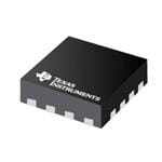
SN54LVC257A,SN74LVC257A www.ti.com SCAS294O–JANUARY1993–REVISEDJUNE2015 5 Device Options PARTNUMBER PACKAGE BODYSIZE SN74LVC257ARGYR VQFN 3.50mm×4.00mm SN74LVC257AD SOIC 3.90mm×9.90mm SN74LVC257ADT SN74LVC257ANSR SO 5.30mm×10.10mm SN74LVC257ADBR SSOP 5.50mm×6.20mm SN74LVC257APW TSSOP 4.40mm×5.00mm SN74LVC257APWT SNJ54LVC257AJ CDIP 6.92mm×21.34mm SNJ54LVC257AW CFP 13.70mm×10.10mm SNJ54LVC257AFK LCCC 8.89mm×8.89mm Copyright©1993–2015,TexasInstrumentsIncorporated SubmitDocumentationFeedback 3 ProductFolderLinks:SN54LVC257A SN74LVC257A
SN54LVC257A,SN74LVC257A SCAS294O–JANUARY1993–REVISEDJUNE2015 www.ti.com 6 Pin Configuration and Functions D,DB,NS,J,W,orPWPackage 16-PinSOIC,SSOP,SO,CDIP,CFP,orTSSOP RGYPackage TopView 16-PinVQFNwithExposedThermalPad TopView A1/AB 12 1165 VOCEC A/B VCC 1B 3 14 4A 1 16 1Y 4 13 4B 1A 2 15 OE 2A 5 12 4Y 1B 3 14 4A 2B 6 11 3A 1Y 4 13 4B 2Y 7 10 3B 2A 5 12 4Y 2B 6 11 3A GND 8 9 3Y 2Y 7 10 3B 8 9 D Y N 3 G FKPackage 20-PinLCCC TopView 1AA/BNCVCCOE 3 2 1 2019 1B 4 18 4A 1Y 5 17 4B NC 6 16 NC 2A 7 15 4Y 2B 8 14 3A 9 10111213 YDCY B 2NN3 3 G PinFunctions PIN SOIC,SSOP,SO, I/O DESCRIPTION NAME CDIP,CFP, LCCC TSSOP,orVQFN A/B 1 2 I SelectPin,LowselectsA,HighselectsB 1A 2 3 I/O MultiplexerSignalInput 1B 3 4 I/O MultiplexerSignalInput 1Y 4 5 I/O MultiplexerOutput 2A 5 7 I/O MultiplexerSignalInput 2B 6 8 I/O MultiplexerSignalInput 2Y 7 9 I/O MultiplexerOutput 3A 11 14 I/O MultiplexerSignalInput 3B 10 13 I/O MultiplexerSignalInput 3Y 9 12 I/O MultiplexerOutput 4A 14 18 I/O MultiplexerSignalInput 4B 13 17 I/O MultiplexerSignalInput 4Y 12 15 I/O MultiplexerOutput GND 8 10 — Ground NC(1) — 1,6,11,16 — Noconnect OE 15 19 I/O ActivelowOutputenable VCC 16 20 — Powerpin (1) NC–nointernalconnection 4 SubmitDocumentationFeedback Copyright©1993–2015,TexasInstrumentsIncorporated ProductFolderLinks:SN54LVC257A SN74LVC257A
SN54LVC257A,SN74LVC257A www.ti.com SCAS294O–JANUARY1993–REVISEDJUNE2015 7 Specifications 7.1 Absolute Maximum Ratings overoperatingfree-airtemperaturerange(unlessotherwisenoted)(1) MIN MAX UNIT V Supplyvoltage –0.5 6.5 V CC V Inputvoltage(2) –0.5 6.5 V I V Outputvoltage(2) (3) –0.5 V +0.5 V O CC I Inputclampcurrent V <0 –50 mA IK I I Outputclampcurrent V <0 –50 mA OK O I Continuousoutputcurrent ±50 mA O ContinuouscurrentthroughV orGND ±100 mA CC T Storagetemperature –65 150 °C stg (1) StressesbeyondthoselistedunderAbsoluteMaximumRatingsmaycausepermanentdamagetothedevice.Thesearestressratings only,whichdonotimplyfunctionaloperationofthedeviceattheseoranyotherconditionsbeyondthoseindicatedunderRecommended OperatingConditions.Exposuretoabsolute-maximum-ratedconditionsforextendedperiodsmayaffectdevicereliability. (2) Theinputnegative-voltageandoutputvoltageratingsmaybeexceedediftheinputandoutputcurrentratingsareobserved. (3) ThevalueofV isprovidedintherecommendedoperatingconditionstable. CC 7.2 ESD Ratings VALUE UNIT Humanbodymodel(HBM),perANSI/ESDA/JEDECJS-001,allpins(1) ±2000 Electrostatic V(ESD) discharge Cpihnasr(g2)ed-devicemodel(CDM),perJEDECspecificationJESD22-C101,all ±1000 V (1) JEDECdocumentJEP155statesthat500-VHBMallowssafemanufacturingwithastandardESDcontrolprocess. (2) JEDECdocumentJEP157statesthat250-VCDMallowssafemanufacturingwithastandardESDcontrolprocess. Copyright©1993–2015,TexasInstrumentsIncorporated SubmitDocumentationFeedback 5 ProductFolderLinks:SN54LVC257A SN74LVC257A
SN54LVC257A,SN74LVC257A SCAS294O–JANUARY1993–REVISEDJUNE2015 www.ti.com 7.3 Recommended Operating Conditions See (1) SN54LVC257A SN74LVC257A UNIT MIN MAX MIN MAX Operating 2 3.6 1.65 3.6 V Supplyvoltage V CC Dataretentiononly 1.5 1.5 V =1.65Vto1.95V 0.65×V CC CC V High-levelinputvoltage V =2.3Vto2.7V 1.7 V IH CC V =2.7Vto3.6V 2 2 CC V =1.65Vto1.95V 0.35×V CC CC V Low-levelinputvoltage V =2.3Vto2.7V 0.7 V IL CC V =2.7Vto3.6V 0.8 0.8 CC V Inputvoltage 0 5.5 0 5.5 V I V Outputvoltage 0 V 0 V V O CC CC V =1.65V –4 CC V =2.3V –8 CC I High-leveloutputcurrent mA OH V =2.7V –12 –12 CC V =3V –24 –24 CC V =1.65V 4 CC V =2.3V 8 CC I Low-leveloutputcurrent mA OL V =2.7V 12 12 CC V =3V 24 24 CC Δt/Δv Inputtransitionriseorfallrate 10 10 ns/V T Operatingfree-airtemperature –55 125 –40 85 °C A (1) AllunusedinputsofthedevicemustbeheldatV orGNDtoensureproperdeviceoperation.RefertotheTIapplicationreport, CC ImplicationsofSloworFloatingCMOSInputs,SCBA004. 7.4 Thermal Information: 16-Pin Packages SN54LVC257A,SN74LVC257A THERMALMETRIC(1) D(SOIC)(2) DB(SSOP)(2) NS(SO)(2) PW(TSSOP)(2) UNIT 16PINS RθJA Junction-to-ambientthermalresistance 73 82 64 108 °C/W (1) Formoreinformationabouttraditionalandnewthermalmetrics,seetheSemiconductorandICPackageThermalMetricsapplication report,SPRA953. (2) ThepackagethermalimpedanceiscalculatedinaccordancewithJESD51-7. 7.5 Thermal Information: 20-Pin Package SN54LVC257A THERMALMETRIC(1) RGY(LCCC)(2) UNIT 20PINS RθJA Junction-to-ambientthermalresistance 39 °C/W (1) Formoreinformationabouttraditionalandnewthermalmetrics,seetheSemiconductorandICPackageThermalMetricsapplication report,SPRA953. (2) ThepackagethermalimpedanceiscalculatedinaccordancewithJESD51-5. 6 SubmitDocumentationFeedback Copyright©1993–2015,TexasInstrumentsIncorporated ProductFolderLinks:SN54LVC257A SN74LVC257A
SN54LVC257A,SN74LVC257A www.ti.com SCAS294O–JANUARY1993–REVISEDJUNE2015 7.6 Electrical Characteristics overrecommendedoperatingfree-airtemperaturerange(unlessotherwisenoted) SN54LVC257A SN74LVC257A PARAMETER TESTCONDITIONS V UNIT CC MIN TYP(1) MAX MIN TYP(1) MAX I =–100μA 1.65Vto3.6V V –0.2 OH CC I =–100μA 2.7Vto3.6V V –0.2 OH CC I =–4mA 1.65V 1.2 OH V I =–8mA 2.3V 1.7 V OH OH 2.7V 2.2 2.2 I =–12mA OH 3V 2.4 2.4 I =–24mA 3V 2.2 2.2 OH 1.65Vto3.6V 0.2 I =100μA OL 2.7Vto3.6V 0.2 I =4mA 1.65V 0.45 OL V V OL I =8mA 2.3V 0.7 OL I =12mA 2.7V 0.4 0.4 OL I =24mA 3V 0.55 0.55 OL I V =5.5VorGND 3.6V ±5 ±5 μA I I I V =V orGND 3.6V ±15 ±10 μA OZ O CC I V =V orGND, I =0 3.6V 10 10 μA CC I CC O OneinputatV –0.6V, ΔI CC 2.7Vto3.6V 500 500 μA CC OtherinputsatV orGND CC C V =V orGND 3.3V 5 5 pF i I CC C V =V orGND 3.3V 5 5 pF o O CC (1) AlltypicalvaluesareatV =3.3V,T =25°C. CC A 7.7 SN54LVC257A Switching Characteristics overrecommendedoperatingfree-airtemperaturerange(unlessotherwisenoted)(seeFigure3) SN54LVC257A FROM TO V =3.3V PARAMETER V =2.7V CC UNIT (INPUT) (OUTPUT) CC ±0.3V MIN MAX MIN MAX AorB 5.4 1 4.6 t Y ns pd A/B 7.5 1 6.4 t OE Y 6.7 1 5.6 ns en t OE Y 4.7 0.5 4.3 ns dis t 1 ns sk(o) 7.8 SN74LVC257A Switching Characteristics overrecommendedoperatingfree-airtemperaturerange(unlessotherwisenoted)(seeFigure3) SN74LVC257A FROM TO V =1.8V V =2.5V V =3.3V PARAMETER CC CC V =2.7V CC UNIT (INPUT) (OUTPUT) ±0.15V ±0.2V CC ±0.3V MIN MAX MIN MAX MIN MAX MIN MAX AorB 1 13.5 1 7.4 1 5.4 1 4.6 t Y ns pd A/B 1 15.6 1 9.5 1 7.5 1 6.4 t OE Y 1 14.6 1 8.7 1 6.7 1 5.6 ns en t OE Y 1 15.4 1 6.7 1 4.7 1 4.3 ns dis t 1 ns sk(o) Copyright©1993–2015,TexasInstrumentsIncorporated SubmitDocumentationFeedback 7 ProductFolderLinks:SN54LVC257A SN74LVC257A
SN54LVC257A,SN74LVC257A SCAS294O–JANUARY1993–REVISEDJUNE2015 www.ti.com 7.9 Operating Characteristics T =25°C A V =1.8V V =2.5V V =3.3V CC CC CC PARAMETER TESTCONDITIONS UNIT TYP TYP TYP C Powerdissipationcapacitance f=10MHz 13.5 14.5 15.5 pF pd 7.10 Typical Characteristics 14 10 VCC=3V, VCC=3V, TA=25°C TA=25°C 12 s –ns OFonuerOOuuttppuuttSswSiwtcithcihnigng e–n 8 OFonuerOOuuttppuuttSswSiwtcithcihnigng Time 10 EightOutputsSwitching yTim EightOutputsSwitching y a ela Del D 8 n 6 n o atio gati g a a 6 p p o o r Pr –P 4 – d d 4 p p t t 2 2 0 50 100 150 200 250 300 0 50 100 150 200 250 300 CL–LoadCapacitance–pF CL–LoadCapacitance–pF Figure1.PropagationDelay(LowtoHighTransition) Figure2.PropagationDelay(HightoLowTransition) vsLoadCapacitance vsLoadCapacitance 8 SubmitDocumentationFeedback Copyright©1993–2015,TexasInstrumentsIncorporated ProductFolderLinks:SN54LVC257A SN74LVC257A
SN54LVC257A,SN74LVC257A www.ti.com SCAS294O–JANUARY1993–REVISEDJUNE2015 8 Parameter Measurement Information VLOAD From Output RL S1 Open TEST S1 Under Test GND tPLH/tPHL Open (see NoteCAL) RL tPLZ/tPZL VLOAD tPHZ/tPZH GND LOAD CIRCUIT INPUTS VCC VI tr/tf VM VLOAD CL RL VΔ 1.8 V±0.15 V VCC ≤2 ns VCC/2 2×VCC 30 pF 1 kΩ 0.15 V 2.5 V±0.2 V VCC ≤2 ns VCC/2 2×VCC 30 pF 500Ω 0.15 V 2.7 V 2.7 V ≤2.5 ns 1.5 V 6 V 50 pF 500Ω 0.3 V 3.3 V±0.3 V 2.7 V ≤2.5 ns 1.5 V 6 V 50 pF 500Ω 0.3 V VI Timing Input VM 0 V tw VI tsu th VI Input VM VM Data Input VM VM 0 V 0 V VOLTAGE WAVEFORMS VOLTAGE WAVEFORMS PULSE DURATION SETUPAND HOLD TIMES VI VI Output Input VM VM Control VM VM 0 V 0 V tPLH tPHL tPZL tPLZ Output VOH Waveform 1 VLOAD/2 Output VM VM VOL (Ss1ee a tN VoLteO ABD) VM VOL+ VΔ VOL tPHL tPLH tPZH tPHZ Output VM VM VOH WSa1v eaOftou GrtmpNu D2t VM VOH−VΔ VOH VOL (see Note B) ≈0 V VOLTAGE WAVEFORMS VOLTAGE WAVEFORMS PROPAGATION DELAYTIMES ENABLEAND DISABLE TIMES INVERTINGAND NONINVERTING OUTPUTS LOW-AND HIGH-LEVELENABLING NOTES: A. CLincludes probe and jig capacitance. B. Waveform 1 is for an output with internal conditions such that the output is low, except when disabled by the output control. Waveform2 is for an output with internal conditions such that the output is high, exceptwhen disabled by the output control. C. All input pulses are supplied by generators having the following characteristics: PRR≤10 MHz, Z O= 50Ω. D. The outputs are measured one at a time, with one transition per measurement. E. tPLZand tPHZare the same as tdis. F. tPZLand tPZHare the same as ten. G. tPLHand tPHLare the same as tpd. H. All parameters and waveforms are not applicable to all devices. Figure3. LoadCircuitandVoltageWaveforms Copyright©1993–2015,TexasInstrumentsIncorporated SubmitDocumentationFeedback 9 ProductFolderLinks:SN54LVC257A SN74LVC257A
SN54LVC257A,SN74LVC257A SCAS294O–JANUARY1993–REVISEDJUNE2015 www.ti.com 9 Detailed Description 9.1 Overview Thesequadruple2-lineto1-linedataselectorsandmultiplexersaredesignedfor1.65-Vto3.6-VV operation. CC The SNx4LVC257A devices are designed to multiplex signals from 4-bit data sources to 4-output data lines in bus-organized systems. The 3-state outputs do not load the data lines when the output-enable (OE) input is at a highlogiclevel. 9.2 Functional Block Diagram 15 OE 1 A/B 2 1A 4 1Y 3 1B 5 2A 7 2Y 6 2B 11 3A 9 3Y 10 3B 14 4A 12 4Y 13 4B 9.3 Feature Description Inputs can be driven from either 3.3-V or 5-V devices. This feature allows the use of these devices as translators inamixed3.3-Vand5-Vsystemenvironment.Devicefeaturesamaximumt of4.6nsallowingthedevicetobe pd usedinhigh-speedapplicationsaswell. To ensure the high-impedance state during power up or power down, OE must be tied to V through a pullup CC resistor;theminimumvalueoftheresistorisdeterminedbythecurrent-sinkingcapabilityofthedriver. 9.4 Device Functional Modes Table1liststhefunctionalmodesfortheSN54LVC257AandSN74LVC257Adevices. Table1.FunctionTable INPUTS OUTPUT OE A/B A B Y H X X X Z L L L X L L L H X H L H X L L L H X H H 10 SubmitDocumentationFeedback Copyright©1993–2015,TexasInstrumentsIncorporated ProductFolderLinks:SN54LVC257A SN74LVC257A
SN54LVC257A,SN74LVC257A www.ti.com SCAS294O–JANUARY1993–REVISEDJUNE2015 10 Application and Implementation NOTE Information in the following applications sections is not part of the TI component specification, and TI does not warrant its accuracy or completeness. TI’s customers are responsible for determining suitability of components for their purposes. Customers should validateandtesttheirdesignimplementationtoconfirmsystemfunctionality. 10.1 Application Information TheSNx4LVC257Adevicesareusefulfordigitalsignaldataselectorormultiplexerapplications. 10.2 Typical Application The SNx4LVC257A devices use CMOS technology and have balanced output drive. These devices can be used fordownleveltranslationandmultiplexerfunctionasshowninFigure4. Vcc=1.65V to 3.6V Vcc=1.65V to 5V 0.1uF Vcc=1.65V to 3.6V Cbypass Vcc A/B Gnd 1Y 1A 1B Processor 1 2Y Digital Signals 2A Or 2B Processor 2 Digital Sensor Array 3Y 3A 3B 4Y 4A 4B OE When 0, Y is high impedance Figure4. SNx4LVC257AUsedasLevelTranslationandasaMultiplexer 10.2.1 DesignRequirements Take care to avoid bus contention because it can drive currents that would exceed maximum limits. The high drive will also create fast edges into light loads so routing and load conditions must be considered to prevent ringing. Copyright©1993–2015,TexasInstrumentsIncorporated SubmitDocumentationFeedback 11 ProductFolderLinks:SN54LVC257A SN74LVC257A
SN54LVC257A,SN74LVC257A SCAS294O–JANUARY1993–REVISEDJUNE2015 www.ti.com Typical Application (continued) 10.2.2 DetailedDesignProcedure 1. RecommendedInputConditions – Forrisetimeandfalltimespecification,see(Δt/ΔV)intheRecommendedOperatingConditions table. – Forspecifiedhighandlowlevels,see(V andV )intheRecommendedOperatingConditions table. IH IL – Inputs are over voltage tolerant allowing them to go as high as (V max) in the Recommended Operating I ConditionstableatanyvalidV . CC 2. RecommendOutputConditions – Load currents must not exceed (I max) per output and must not exceed (continuous current through V O CC orGND)totalcurrentforthepart.TheselimitsareintheRecommendedOperatingConditions table. – OutputsmustnotbepulledaboveV . CC 10.2.3 ApplicationCurves 100 60 TA=25°C,VCC=3V, TA=25°C,VCC=3V, VIH=3V,VIL=0V, 40 VIH=3V,VIL=0V, 80 AllOutputsSwitching AllOutputsSwitching 20 60 0 A A m m – 40 – –20 OL OH I I –40 20 –60 0 –80 –20 –100 –0.2 0.0 0.2 0.4 0.6 0.8 1.0 1.2 1.4 1.6 –1 –0.5 0.0 0.5 1.0 1.5 2.0 2.5 3.0 3.5 4.0 VOL–V VOH–V Figure5.OutputDriveCurrent(IOL) Figure6.OutputDriveCurrent(IOH) vsLOW-levelOutputVoltage(VOL) vsHIGH-levelOutputVoltage(VOH) 12 SubmitDocumentationFeedback Copyright©1993–2015,TexasInstrumentsIncorporated ProductFolderLinks:SN54LVC257A SN74LVC257A
SN54LVC257A,SN74LVC257A www.ti.com SCAS294O–JANUARY1993–REVISEDJUNE2015 11 Power Supply Recommendations The power supply can be any voltage between the minimum and maximum supply voltage rating located in the RecommendedOperatingConditionstable. Each V terminal must have a good bypass capacitor to prevent power disturbance. For devices with a single CC supply, a 0.1-μF capacitor is recommended. If there are multiple V terminals then 0.01-μF or 0.022-μF CC capacitors are recommended for each power terminal. It is ok to parallel multiple bypass capacitors to reject different frequencies of noise. Multiple bypass capacitors may be paralleled to reject different frequencies of noise.Thebypasscapacitormustbeinstalledasclosetothepowerterminalaspossibleforthebestresults. 12 Layout 12.1 Layout Guidelines When using multiple bit logic devices, inputs must not float. In many cases, functions or parts of functions of digital logic devices are unused. Some examples are when only two inputs of a triple-input AND gate are used, or when only 3 of the 4-buffer gates are used. Such input pins must not be left unconnected because the undefinedvoltagesattheoutsideconnectionsresultinundefinedoperationalstates. Specified in Figure 7 are rules that must be observed under all circumstances. All unused inputs of digital logic devices must be connected to a high or low bias to prevent them from floating. The logic level that must be applied to any particular unused input depends on the function of the device. Generally they will be tied to GND orV ,whichevermakesmoresenseorismoreconvenient. CC 12.2 Layout Example VCC Input Unused Input Output Unused Input Output Input Figure7. LayoutDiagrams Copyright©1993–2015,TexasInstrumentsIncorporated SubmitDocumentationFeedback 13 ProductFolderLinks:SN54LVC257A SN74LVC257A
SN54LVC257A,SN74LVC257A SCAS294O–JANUARY1993–REVISEDJUNE2015 www.ti.com 13 Device and Documentation Support 13.1 Documentation Support 13.1.1 RelatedDocumentation Forrelateddocumentationseethefollowing: ImplicationsofSloworFloatingCMOSInputs,SCBA004 13.2 Related Links The table below lists quick access links. Categories include technical documents, support and community resources,toolsandsoftware,andquickaccesstosampleorbuy. Table2.RelatedLinks TECHNICAL TOOLS& SUPPORT& PARTS PRODUCTFOLDER SAMPLE&BUY DOCUMENTS SOFTWARE COMMUNITY SN54LVC257A Clickhere Clickhere Clickhere Clickhere Clickhere SN74LVC257A Clickhere Clickhere Clickhere Clickhere Clickhere 13.3 Community Resources The following links connect to TI community resources. Linked contents are provided "AS IS" by the respective contributors. They do not constitute TI specifications and do not necessarily reflect TI's views; see TI's Terms of Use. TIE2E™OnlineCommunity TI'sEngineer-to-Engineer(E2E)Community.Createdtofostercollaboration amongengineers.Ate2e.ti.com,youcanaskquestions,shareknowledge,exploreideasandhelp solveproblemswithfellowengineers. DesignSupport TI'sDesignSupport QuicklyfindhelpfulE2Eforumsalongwithdesignsupporttoolsand contactinformationfortechnicalsupport. 13.4 Trademarks E2EisatrademarkofTexasInstruments. Allothertrademarksarethepropertyoftheirrespectiveowners. 13.5 Electrostatic Discharge Caution Thesedeviceshavelimitedbuilt-inESDprotection.Theleadsshouldbeshortedtogetherorthedeviceplacedinconductivefoam duringstorageorhandlingtopreventelectrostaticdamagetotheMOSgates. 13.6 Glossary SLYZ022—TIGlossary. Thisglossarylistsandexplainsterms,acronyms,anddefinitions. 14 Mechanical, Packaging, and Orderable Information The following pages include mechanical packaging and orderable information. This information is the most current data available for the designated devices. This data is subject to change without notice and revision of thisdocument.Forbrowserbasedversionsofthisdatasheet,refertothelefthandnavigation. 14 SubmitDocumentationFeedback Copyright©1993–2015,TexasInstrumentsIncorporated ProductFolderLinks:SN54LVC257A SN74LVC257A
PACKAGE OPTION ADDENDUM www.ti.com 24-Aug-2018 PACKAGING INFORMATION Orderable Device Status Package Type Package Pins Package Eco Plan Lead/Ball Finish MSL Peak Temp Op Temp (°C) Device Marking Samples (1) Drawing Qty (2) (6) (3) (4/5) 5962-0050901QFA ACTIVE CFP W 16 1 TBD A42 N / A for Pkg Type -55 to 125 5962-0050901QF A SNJ54LVC257AW SN74LVC257AD ACTIVE SOIC D 16 40 Green (RoHS CU NIPDAU Level-1-260C-UNLIM -40 to 85 LVC257A & no Sb/Br) SN74LVC257ADBR ACTIVE SSOP DB 16 2000 Green (RoHS CU NIPDAU Level-1-260C-UNLIM -40 to 85 LC257A & no Sb/Br) SN74LVC257ADBRG4 ACTIVE SSOP DB 16 2000 Green (RoHS CU NIPDAU Level-1-260C-UNLIM -40 to 85 LC257A & no Sb/Br) SN74LVC257ADR ACTIVE SOIC D 16 2500 Green (RoHS CU NIPDAU Level-1-260C-UNLIM -40 to 85 LVC257A & no Sb/Br) SN74LVC257ADRG4 ACTIVE SOIC D 16 2500 Green (RoHS CU NIPDAU Level-1-260C-UNLIM -40 to 85 LVC257A & no Sb/Br) SN74LVC257ANSR ACTIVE SO NS 16 2000 Green (RoHS CU NIPDAU Level-1-260C-UNLIM -40 to 85 LVC257A & no Sb/Br) SN74LVC257APW ACTIVE TSSOP PW 16 90 Green (RoHS CU NIPDAU Level-1-260C-UNLIM -40 to 85 LC257A & no Sb/Br) SN74LVC257APWR ACTIVE TSSOP PW 16 2000 Green (RoHS CU NIPDAU | CU SN Level-1-260C-UNLIM -40 to 85 LC257A & no Sb/Br) SN74LVC257APWRG4 ACTIVE TSSOP PW 16 2000 Green (RoHS CU NIPDAU Level-1-260C-UNLIM -40 to 85 LC257A & no Sb/Br) SN74LVC257APWT ACTIVE TSSOP PW 16 250 Green (RoHS CU NIPDAU Level-1-260C-UNLIM -40 to 85 LC257A & no Sb/Br) SN74LVC257ARGYR ACTIVE VQFN RGY 16 3000 Green (RoHS CU NIPDAU Level-2-260C-1 YEAR -40 to 85 LC257A & no Sb/Br) SNJ54LVC257AW ACTIVE CFP W 16 1 TBD A42 N / A for Pkg Type -55 to 125 5962-0050901QF A SNJ54LVC257AW (1) The marketing status values are defined as follows: ACTIVE: Product device recommended for new designs. LIFEBUY: TI has announced that the device will be discontinued, and a lifetime-buy period is in effect. NRND: Not recommended for new designs. Device is in production to support existing customers, but TI does not recommend using this part in a new design. PREVIEW: Device has been announced but is not in production. Samples may or may not be available. OBSOLETE: TI has discontinued the production of the device. Addendum-Page 1
PACKAGE OPTION ADDENDUM www.ti.com 24-Aug-2018 (2) RoHS: TI defines "RoHS" to mean semiconductor products that are compliant with the current EU RoHS requirements for all 10 RoHS substances, including the requirement that RoHS substance do not exceed 0.1% by weight in homogeneous materials. Where designed to be soldered at high temperatures, "RoHS" products are suitable for use in specified lead-free processes. TI may reference these types of products as "Pb-Free". RoHS Exempt: TI defines "RoHS Exempt" to mean products that contain lead but are compliant with EU RoHS pursuant to a specific EU RoHS exemption. Green: TI defines "Green" to mean the content of Chlorine (Cl) and Bromine (Br) based flame retardants meet JS709B low halogen requirements of <=1000ppm threshold. Antimony trioxide based flame retardants must also meet the <=1000ppm threshold requirement. (3) MSL, Peak Temp. - The Moisture Sensitivity Level rating according to the JEDEC industry standard classifications, and peak solder temperature. (4) There may be additional marking, which relates to the logo, the lot trace code information, or the environmental category on the device. (5) Multiple Device Markings will be inside parentheses. Only one Device Marking contained in parentheses and separated by a "~" will appear on a device. If a line is indented then it is a continuation of the previous line and the two combined represent the entire Device Marking for that device. (6) Lead/Ball Finish - Orderable Devices may have multiple material finish options. Finish options are separated by a vertical ruled line. Lead/Ball Finish values may wrap to two lines if the finish value exceeds the maximum column width. Important Information and Disclaimer:The information provided on this page represents TI's knowledge and belief as of the date that it is provided. TI bases its knowledge and belief on information provided by third parties, and makes no representation or warranty as to the accuracy of such information. Efforts are underway to better integrate information from third parties. TI has taken and continues to take reasonable steps to provide representative and accurate information but may not have conducted destructive testing or chemical analysis on incoming materials and chemicals. TI and TI suppliers consider certain information to be proprietary, and thus CAS numbers and other limited information may not be available for release. In no event shall TI's liability arising out of such information exceed the total purchase price of the TI part(s) at issue in this document sold by TI to Customer on an annual basis. OTHER QUALIFIED VERSIONS OF SN54LVC257A, SN74LVC257A : •Catalog: SN74LVC257A •Automotive: SN74LVC257A-Q1, SN74LVC257A-Q1 •Enhanced Product: SN74LVC257A-EP, SN74LVC257A-EP •Military: SN54LVC257A NOTE: Qualified Version Definitions: •Catalog - TI's standard catalog product Addendum-Page 2
PACKAGE OPTION ADDENDUM www.ti.com 24-Aug-2018 •Automotive - Q100 devices qualified for high-reliability automotive applications targeting zero defects •Enhanced Product - Supports Defense, Aerospace and Medical Applications •Military - QML certified for Military and Defense Applications Addendum-Page 3
PACKAGE MATERIALS INFORMATION www.ti.com 20-Dec-2018 TAPE AND REEL INFORMATION *Alldimensionsarenominal Device Package Package Pins SPQ Reel Reel A0 B0 K0 P1 W Pin1 Type Drawing Diameter Width (mm) (mm) (mm) (mm) (mm) Quadrant (mm) W1(mm) SN74LVC257ADR SOIC D 16 2500 330.0 16.4 6.5 10.3 2.1 8.0 16.0 Q1 SN74LVC257ANSR SO NS 16 2000 330.0 16.4 8.2 10.5 2.5 12.0 16.0 Q1 SN74LVC257APWR TSSOP PW 16 2000 330.0 12.4 6.9 5.6 1.6 8.0 12.0 Q1 SN74LVC257APWR TSSOP PW 16 2000 330.0 12.4 6.9 5.6 1.6 8.0 12.0 Q1 SN74LVC257APWRG4 TSSOP PW 16 2000 330.0 12.4 6.9 5.6 1.6 8.0 12.0 Q1 SN74LVC257APWT TSSOP PW 16 250 330.0 12.4 6.9 5.6 1.6 8.0 12.0 Q1 SN74LVC257ARGYR VQFN RGY 16 3000 330.0 12.4 3.8 4.3 1.5 8.0 12.0 Q1 PackMaterials-Page1
PACKAGE MATERIALS INFORMATION www.ti.com 20-Dec-2018 *Alldimensionsarenominal Device PackageType PackageDrawing Pins SPQ Length(mm) Width(mm) Height(mm) SN74LVC257ADR SOIC D 16 2500 333.2 345.9 28.6 SN74LVC257ANSR SO NS 16 2000 367.0 367.0 38.0 SN74LVC257APWR TSSOP PW 16 2000 364.0 364.0 27.0 SN74LVC257APWR TSSOP PW 16 2000 367.0 367.0 35.0 SN74LVC257APWRG4 TSSOP PW 16 2000 367.0 367.0 35.0 SN74LVC257APWT TSSOP PW 16 250 367.0 367.0 35.0 SN74LVC257ARGYR VQFN RGY 16 3000 367.0 367.0 35.0 PackMaterials-Page2
None
None
PACKAGE OUTLINE PW0016A TSSOP - 1.2 mm max height SCALE 2.500 SMALL OUTLINE PACKAGE SEATING PLANE C 6.6 TYP 6.2 A 0.1 C PIN 1 INDEX AREA 14X 0.65 16 1 2X 5.1 4.55 4.9 NOTE 3 8 9 0.30 B 4.5 16X 0.19 1.2 MAX 4.3 0.1 C A B NOTE 4 (0.15) TYP SEE DETAIL A 0.25 GAGE PLANE 0.15 0.05 0.75 0.50 0 -8 DETA 20AIL A TYPICAL 4220204/A 02/2017 NOTES: 1. All linear dimensions are in millimeters. Any dimensions in parenthesis are for reference only. Dimensioning and tolerancing per ASME Y14.5M. 2. This drawing is subject to change without notice. 3. This dimension does not include mold flash, protrusions, or gate burrs. Mold flash, protrusions, or gate burrs shall not exceed 0.15 mm per side. 4. This dimension does not include interlead flash. Interlead flash shall not exceed 0.25 mm per side. 5. Reference JEDEC registration MO-153. www.ti.com
EXAMPLE BOARD LAYOUT PW0016A TSSOP - 1.2 mm max height SMALL OUTLINE PACKAGE 16X (1.5) SYMM (R0.05) TYP 1 16X (0.45) 16 SYMM 14X (0.65) 8 9 (5.8) LAND PATTERN EXAMPLE EXPOSED METAL SHOWN SCALE: 10X SOLDER MASK METAL UNDER SOLDER MASK OPENING METAL SOLDER MASK OPENING EXPOSED METAL EXPOSED METAL 0.05 MAX 0.05 MIN ALL AROUND ALL AROUND NON-SOLDER MASK SOLDER MASK DEFINED DEFINED (PREFERRED) SOLDE15.000R MASK DETAILS 4220204/A 02/2017 NOTES: (continued) 6. Publication IPC-7351 may have alternate designs. 7. Solder mask tolerances between and around signal pads can vary based on board fabrication site. www.ti.com
EXAMPLE STENCIL DESIGN PW0016A TSSOP - 1.2 mm max height SMALL OUTLINE PACKAGE 16X (1.5) SYMM (R0.05) TYP 1 16X (0.45) 16 SYMM 14X (0.65) 8 9 (5.8) SOLDER PASTE EXAMPLE BASED ON 0.125 mm THICK STENCIL SCALE: 10X 4220204/A 02/2017 NOTES: (continued) 8. Laser cutting apertures with trapezoidal walls and rounded corners may offer better paste release. IPC-7525 may have alternate design recommendations. 9. Board assembly site may have different recommendations for stencil design. www.ti.com
None
None
MECHANICAL DATA MSSO002E – JANUARY 1995 – REVISED DECEMBER 2001 DB (R-PDSO-G**) PLASTIC SMALL-OUTLINE 28 PINS SHOWN 0,38 0,65 0,15 M 0,22 28 15 0,25 0,09 5,60 8,20 5,00 7,40 Gage Plane 1 14 0,25 A 0°–(cid:1)8° 0,95 0,55 Seating Plane 2,00 MAX 0,05 MIN 0,10 PINS ** 14 16 20 24 28 30 38 DIM A MAX 6,50 6,50 7,50 8,50 10,50 10,50 12,90 A MIN 5,90 5,90 6,90 7,90 9,90 9,90 12,30 4040065/E 12/01 NOTES: A. All linear dimensions are in millimeters. B. This drawing is subject to change without notice. C. Body dimensions do not include mold flash or protrusion not to exceed 0,15. D. Falls within JEDEC MO-150 • POST OFFICE BOX 655303 DALLAS, TEXAS 75265
None
None
None
IMPORTANTNOTICEANDDISCLAIMER TIPROVIDESTECHNICALANDRELIABILITYDATA(INCLUDINGDATASHEETS),DESIGNRESOURCES(INCLUDINGREFERENCE DESIGNS),APPLICATIONOROTHERDESIGNADVICE,WEBTOOLS,SAFETYINFORMATION,ANDOTHERRESOURCES“ASIS” ANDWITHALLFAULTS,ANDDISCLAIMSALLWARRANTIES,EXPRESSANDIMPLIED,INCLUDINGWITHOUTLIMITATIONANY IMPLIEDWARRANTIESOFMERCHANTABILITY,FITNESSFORAPARTICULARPURPOSEORNON-INFRINGEMENTOFTHIRD PARTYINTELLECTUALPROPERTYRIGHTS. TheseresourcesareintendedforskilleddevelopersdesigningwithTIproducts.Youaresolelyresponsiblefor(1)selectingtheappropriate TIproductsforyourapplication,(2)designing,validatingandtestingyourapplication,and(3)ensuringyourapplicationmeetsapplicable standards,andanyothersafety,security,orotherrequirements.Theseresourcesaresubjecttochangewithoutnotice.TIgrantsyou permissiontousetheseresourcesonlyfordevelopmentofanapplicationthatusestheTIproductsdescribedintheresource.Other reproductionanddisplayoftheseresourcesisprohibited.NolicenseisgrantedtoanyotherTIintellectualpropertyrightortoanythird partyintellectualpropertyright.TIdisclaimsresponsibilityfor,andyouwillfullyindemnifyTIanditsrepresentativesagainst,anyclaims, damages,costs,losses,andliabilitiesarisingoutofyouruseoftheseresources. TI’sproductsareprovidedsubjecttoTI’sTermsofSale(www.ti.com/legal/termsofsale.html)orotherapplicabletermsavailableeitheron ti.comorprovidedinconjunctionwithsuchTIproducts.TI’sprovisionoftheseresourcesdoesnotexpandorotherwisealterTI’sapplicable warrantiesorwarrantydisclaimersforTIproducts. MailingAddress:TexasInstruments,PostOfficeBox655303,Dallas,Texas75265 Copyright©2018,TexasInstrumentsIncorporated