ICGOO在线商城 > 集成电路(IC) > 逻辑 - 缓冲器,驱动器,接收器,收发器 > SN74LVC244ADGVR
 Datasheet下载
- 型号: SN74LVC244ADGVR
- 制造商: Texas Instruments
- 库位|库存: xxxx|xxxx
- 要求:
| 数量阶梯 | 香港交货 | 国内含税 |
| +xxxx | $xxxx | ¥xxxx |
查看当月历史价格
查看今年历史价格
SN74LVC244ADGVR产品简介:
ICGOO电子元器件商城为您提供SN74LVC244ADGVR由Texas Instruments设计生产,在icgoo商城现货销售,并且可以通过原厂、代理商等渠道进行代购。 SN74LVC244ADGVR价格参考¥1.01-¥2.89。Texas InstrumentsSN74LVC244ADGVR封装/规格:逻辑 - 缓冲器,驱动器,接收器,收发器, Buffer, Non-Inverting 2 Element 4 Bit per Element 3-State Output 20-TVSOP。您可以下载SN74LVC244ADGVR参考资料、Datasheet数据手册功能说明书,资料中有SN74LVC244ADGVR 详细功能的应用电路图电压和使用方法及教程。
SN74LVC244ADGVR 是由 Texas Instruments(德州仪器)生产的一款逻辑缓冲器芯片,属于 SN74LVC 系列。它广泛应用于需要信号缓冲、电平转换和驱动能力增强的场景。以下是其主要应用场景:

 1. 信号缓冲与隔离
   - 在复杂的数字电路中,信号可能需要经过长距离传输或分发到多个负载。SN74LVC244ADGVR 可以用作信号缓冲器,确保输出信号的完整性,同时减少输入端的负载影响。
   - 适用于多点通信系统,例如总线结构中的数据分发。

 2. 电平转换
   - 支持 1.65V 至 5.5V 的宽电压范围,使其非常适合在不同电压域之间进行电平转换。例如,在低功耗 MCU(如 3.3V 系统)与高电压外设(如 5V 设备)之间实现兼容性。

 3. 驱动能力增强
   - 提供较高的驱动能力,能够驱动更多负载或更长的线路。适用于驱动 LED、继电器、小型电机等需要较大电流的设备。
   - 在音频或视频信号传输中,可作为驱动级增强信号强度。

 4. 数据总线扩展
   - 常用于计算机或嵌入式系统的数据总线扩展,将单个数据源分发到多个目标设备。
   - 例如,在内存扩展或外设接口设计中,可以用来增强数据总线的驱动能力。

 5. 工业控制
   - 在工业自动化领域,可用于 PLC(可编程逻辑控制器)、传感器接口和通信模块中,提供可靠的信号处理和驱动功能。
   - 适用于恶劣环境下的信号传输,具有良好的抗干扰能力。

 6. 消费电子
   - 应用于电视、显示器、打印机等消费电子产品中,作为信号缓冲和驱动组件。
   - 在音频设备中,可用来增强信号输出能力,确保高质量的音频传输。

 7. 通信接口
   - 在 UART、SPI、I²C 等通信接口中,可以用作信号增强器,延长通信距离或提高信号质量。
   - 支持双向通信模式(通过外部上下拉电阻配置),适合某些特定的收发器应用。

 总结
SN74LVC244ADGVR 的典型应用场景包括信号缓冲、电平转换、驱动能力增强、数据总线扩展以及工业和消费电子领域的信号处理。其低功耗、高可靠性和宽电压范围特性,使其成为许多现代电子系统中不可或缺的组件。
| 参数 | 数值 |
| 产品目录 | 集成电路 (IC)半导体 |
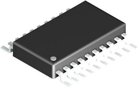
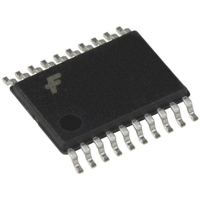
| 描述 | IC BUFF/DVR TRI-ST DUAL 20TVSOP缓冲器和线路驱动器 Tri-State Octal |
| 产品分类 | |
| 品牌 | Texas Instruments |
| 产品手册 | |
| 产品图片 |
|
| rohs | 符合RoHS无铅 / 符合限制有害物质指令(RoHS)规范要求 |
| 产品系列 | 逻辑集成电路,缓冲器和线路驱动器,Texas Instruments SN74LVC244ADGVR74LVC |
| 数据手册 | |
| 产品型号 | SN74LVC244ADGVR |
| 产品目录页面 | |
| 产品种类 | 缓冲器和线路驱动器 |
| 传播延迟时间 | 6.7 ns at 2.7 V, 5.7 ns at 3.3 V |
| 低电平输出电流 | 24 mA |
| 供应商器件封装 | 20-TVSOP |
| 元件数 | 2 |
| 其它名称 | 296-8500-6 |
| 包装 | Digi-Reel® |
| 单位重量 | 60.200 mg |
| 商标 | Texas Instruments |
| 安装类型 | 表面贴装 |
| 安装风格 | SMD/SMT |
| 封装 | Reel |
| 封装/外壳 | 20-TFSOP(0.173",4.40mm 宽) |
| 封装/箱体 | TVSOP-20 |
| 工作温度 | -40°C ~ 125°C |
| 工厂包装数量 | 2000 |
| 最大功率耗散 | 500 mW |
| 最大工作温度 | + 125 C |
| 最小工作温度 | - 40 C |
| 极性 | Non-Inverting |
| 标准包装 | 1 |
| 每元件位数 | 4 |
| 每芯片的通道数量 | 8 |
| 电压-电源 | 1.65 V ~ 3.6 V |
| 电流-输出高,低 | 24mA,24mA |
| 电源电压-最大 | 3.6 V |
| 电源电压-最小 | 1.65 V |
| 电源电流 | 0.01 mA |
| 系列 | SN74LVC244A |
| 输入线路数量 | 8 |
| 输出类型 | 3-State |
| 输出线路数量 | 3 |
| 逻辑类型 | 缓冲器/线路驱动器,非反相 |
| 逻辑系列 | LVC |
| 高电平输出电流 | - 24 mA |


- 商务部:美国ITC正式对集成电路等产品启动337调查
- 曝三星4nm工艺存在良率问题 高通将骁龙8 Gen1或转产台积电
- 太阳诱电将投资9.5亿元在常州建新厂生产MLCC 预计2023年完工
- 英特尔发布欧洲新工厂建设计划 深化IDM 2.0 战略
- 台积电先进制程称霸业界 有大客户加持明年业绩稳了
- 达到5530亿美元!SIA预计今年全球半导体销售额将创下新高
- 英特尔拟将自动驾驶子公司Mobileye上市 估值或超500亿美元
- 三星加码芯片和SET,合并消费电子和移动部门,撤换高东真等 CEO
- 三星电子宣布重大人事变动 还合并消费电子和移动部门
- 海关总署:前11个月进口集成电路产品价值2.52万亿元 增长14.8%


PDF Datasheet 数据手册内容提取
Product Sample & Technical Tools & Support & Folder Buy Documents Software Community SN74LVC244A SCAS414AB–NOVEMBER1992–REVISEDNOVEMBER2016 SN74LVC244A Octal Buffer or Driver With 3-State Outputs 1 Features 2 Applications • OperatesFrom1.65Vto3.6V • Servers 1 • InputsAcceptVoltagesto5.5V • LEDDisplays • SpecifiedFrom–40°Cto+85°Cand • NetworkSwitches –40°Cto+125°C • TelecomInfrastructure • Maximumtpdof5.9nsat3.3V • MotorDrivers • TypicalVOLP (OutputGroundBounce) • I/OExpanders <0.8VatV =3.3V,T =25°C CC A • TypicalV (OutputV Undershoot) 3 Description OHV OH >2VatV =3.3V,T =25°C These octal bus buffers are designed for 1.65-V to CC A • SupportsMixed-ModeSignalOperationon 3.6-V VCC operation. The SN74LVC244A devices are designed for asynchronous communication AllPorts(5-VInputorOutputVoltageWith betweendatabuses. 3.3-VV ) CC • I SupportsLiveInsertion,Partial-Power-Down off DeviceInformation Mode,andBack-DriveProtection PARTNUMBER PACKAGE BODYSIZE(NOM) • CanBeUsedasaDownTranslatortoTranslate SN74LVC244AN PDIP(20) 25.40mm×6.35mm InputsFromaMaximumof5.5VDown SN74LVC244ANS SO(20) 12.60mm×5.30mm totheV Level CC SN74LVC244ADB SSOP(20) 7.50mm×5.30mm • AvailableinUltraSmallLogicQFNPackage(0.5 SN74LVC244ADGV TVSOP(20) 5.00mm×4.40mm mmMaximumHeight) SN74LVC244ADW SOIC(20) 12.80mm×7.50mm • Latch-UpPerformanceExceeds250mAPer SN74LVC244ARGY VQFN(20) 4.50mm×3.50mm JESD17 SN74LVC244AZQN BGA(20) 3.00mm×4.00mm • ESDProtectionExceedsJESD22 SN74LVC244APW TSSOP(20) 6.50mm×4.40mm SN74LVC244ARWP X1QFN(20) 2.50mm×3.30mm – 2000-VHuman-BodyModel – 1000-VCharged-DeviceModel (1) For all available packages, see the orderable addendum at theendofthedatasheet. LogicDiagram(PositiveLogic) 1 19 1OE 2OE 2 18 11 9 1A1 1Y1 2A1 2Y1 4 16 13 7 1A2 1Y2 2A2 2Y2 6 14 15 5 1A3 1Y3 2A3 2Y3 8 12 17 3 1A4 1Y4 2A4 2Y4 Pin numbers shown are for the DB, DGV, DW, N, NS, PW, and RGYpackages. 1 An IMPORTANT NOTICE at the end of this data sheet addresses availability, warranty, changes, use in safety-critical applications, intellectualpropertymattersandotherimportantdisclaimers.PRODUCTIONDATA.
SN74LVC244A SCAS414AB–NOVEMBER1992–REVISEDNOVEMBER2016 www.ti.com Table of Contents 1 Features.................................................................. 1 8.2 FunctionalBlockDiagram.........................................9 2 Applications........................................................... 1 8.3 FeatureDescription...................................................9 3 Description............................................................. 1 8.4 DeviceFunctionalModes..........................................9 4 RevisionHistory..................................................... 2 9 ApplicationandImplementation........................ 10 9.1 ApplicationInformation............................................10 5 PinConfigurationandFunctions......................... 3 9.2 TypicalApplication .................................................10 6 Specifications......................................................... 4 10 PowerSupplyRecommendations..................... 11 6.1 AbsoluteMaximumRatings......................................4 11 Layout................................................................... 11 6.2 ESDRatings..............................................................5 6.3 RecommendedOperatingConditions.......................5 11.1 LayoutGuidelines.................................................11 6.4 ThermalInformation..................................................5 11.2 LayoutExample....................................................11 6.5 ElectricalCharacteristics...........................................6 12 DeviceandDocumentationSupport................. 12 6.6 SwitchingCharacteristics..........................................6 12.1 ReceivingNotificationofDocumentationUpdates12 6.7 OperatingCharacteristics..........................................7 12.2 CommunityResources..........................................12 6.8 TypicalCharacteristics..............................................7 12.3 Trademarks...........................................................12 7 ParameterMeasurementInformation..................8 12.4 ElectrostaticDischargeCaution............................12 12.5 Glossary................................................................12 8 DetailedDescription.............................................. 9 13 Mechanical,Packaging,andOrderable 8.1 Overview...................................................................9 Information........................................................... 12 4 Revision History NOTE:Pagenumbersforpreviousrevisionsmaydifferfrompagenumbersinthecurrentversion. ChangesfromRevisionAA(June2016)toRevisionAB Page • ChangedA2toA4for2OEinPinFunctionstable................................................................................................................. 4 • Addedambienttemperature,T forBGApackageandallotherpackagesinRecommendedOperatingConditions...........5 A • AddedReceivingNotificationofDocumentationUpdatessection....................................................................................... 12 ChangesfromRevisionZ(January2015)toRevisionAA Page • UpdatedDeviceInformationtabletoshowallavailablepackages........................................................................................ 1 • AddedRWPPackage ............................................................................................................................................................ 3 • DeletedGQNpackagefromPinFunctionstable................................................................................................................... 4 • AddedRWPthermalinformationtoThermalInformationtableandupdatedallthermalinformationforexistingpackages.5 • UpdatedallvaluesforZQNcolumninThermalInformationtable......................................................................................... 5 • AddedpackagetypeinThermalInformationtable................................................................................................................. 5 • AddedRWPthermalinformationtoThermalInformationtableandupdatedallthermalinformationforexistingpackages.6 • UpdatedallvaluesforZQNcolumninThermalInformationtable......................................................................................... 6 • AddedpackagetypeinThermalInformationtable................................................................................................................. 6 ChangesfromRevisionY(September2010)toRevisionZ Page • AddedApplications,DeviceInformationtable,PinFunctionstable,ESDRatingstable,ThermalInformationtable, TypicalCharacteristics,FeatureDescriptionsection,DeviceFunctionalModes,ApplicationandImplementation section,PowerSupplyRecommendationssection,Layoutsection,DeviceandDocumentationSupportsection,and Mechanical,Packaging,andOrderableInformationsection.................................................................................................. 1 • DeletedOrderingInformationtable,seeMechanical,Packaging,andOrderableInformationattheendofthedatasheet..1 • UpdatedFeatures................................................................................................................................................................... 1 2 SubmitDocumentationFeedback Copyright©1992–2016,TexasInstrumentsIncorporated ProductFolderLinks:SN74LVC244A
SN74LVC244A www.ti.com SCAS414AB–NOVEMBER1992–REVISEDNOVEMBER2016 5 Pin Configuration and Functions ZQNPackage DB,DGV,DW,N,NS,andPWPackages 20-PinBGA 20-PinSSOP,TVSOP,SOIC,PDIP,SO,andTSSOP TopView FrontView 1 2 3 4 1OE 1 20 V CC A 1A1 1OE VCC 2OE 1A1 2 19 2OE 2Y4 3 18 1Y1 B 1A2 2A4 2Y4 1Y1 1A2 4 17 2A4 2Y3 5 16 1Y2 1A3 6 15 2A3 C 1A3 2Y3 2A3 1Y2 2Y2 7 14 1Y3 1A4 8 13 2A2 D 1A4 2A2 2Y2 1Y3 2Y1 9 12 1Y4 GND 10 11 2A1 E GND 2Y1 2A1 1Y4 Not to scale Not to scale RGYPackage RWPPackage 20-PinVQFN 20-PinX1QFN TopView TopView E C E CE 1 O C O CO Y 1 V 1 V 2 1 1 0 0 9 8 7 1A1 2 219 2OE 1A1 1 2 1 1 116 2A4 2Y4 3 18 1Y1 2Y4 2 15 1Y2 Thermal 1A2 4 17 2A4 1A2 3 14 2A3 Pad 2Y3 5 Thermal 16 1Y2 2Y3 4 13 1Y3 Pad 1A3 6 15 2A3 1A3 5 12 2A2 2Y2 7 14 1Y3 2Y2 6 11 1Y4 0 1A4 8 13 2A2 7 8 9 1 2Y1 9 12 1Y4 0 1 1 1 4 1 D 1 A Y N A 1 2 G 2 Not to scale D 1 N A G 2 Not to scale TIrecommendstoconnecttheexposedthermalpadtogroundforbestthermalperformance.Mustnotbeconnected toanyotherpinthanground. Copyright©1992–2016,TexasInstrumentsIncorporated SubmitDocumentationFeedback 3 ProductFolderLinks:SN74LVC244A
SN74LVC244A SCAS414AB–NOVEMBER1992–REVISEDNOVEMBER2016 www.ti.com PinFunctions PIN DB,DGV, DW,N,NS, TYPE DESCRIPTION NAME ZQN RWP PW,and RGY 1A1 2 A1 1 I Port1A1input 1A2 4 B1 3 I Port1A2input 1A3 6 C1 5 I Port1A3input 1A4 8 D1 7 I Port1A4input 1OE 1 A2 20 I Outputenable 1Y1 18 B4 17 O Port1Y1output 1Y2 16 C4 15 O Port1Y2output 1Y3 14 D4 13 O Port1Y3output 1Y4 12 E4 11 O Port1Y4output 2A1 11 E3 10 I Port2A1input 2A2 13 D2 12 I Port2A2input 2A3 15 C3 14 I Port2A3input 2A4 17 B2 16 I Port2A4input 2OE 19 A4 18 I Outputenable 2Y1 9 E2 8 O Port2Y1output 2Y2 7 D3 6 O Port2Y2output 2Y3 5 C2 4 O Port2Y3output 2Y4 3 B3 2 O Port2Y4output GND 10 E1 9 — Ground VCC 20 A3 19 — Powerpin 6 Specifications 6.1 Absolute Maximum Ratings overoperatingfree-airtemperaturerange(unlessotherwisenoted)(1) MIN MAX UNIT V Supplyvoltage –0.5 6.5 V CC V Inputvoltage(2) –0.5 6.5 V I V Voltagerangeappliedtoanyoutputinthehigh-impedanceorpower-offstate(2) –0.5 6.5 V O V Voltagerangeappliedtoanyoutputinthehighorlowstate(2)(3) –0.5 V +0.5 V O CC I Inputclampcurrent V <0 –50 mA IK I I Outputclampcurrent V <0 –50 mA OK O I Continuousoutputcurrent ±50 mA O ContinuouscurrentthroughV orGND ±100 mA CC P Powerdissipation T =–40°Cto+125°C(4)(5) 500 mW tot A T Junctiontemperature 150 °C J T Storagetemperature –65 150 °C stg (1) StressesbeyondthoselistedunderAbsoluteMaximumRatingsmaycausepermanentdamagetothedevice.Thesearestressratings only,andfunctionaloperationofthedeviceattheseoranyotherconditionsbeyondthoseindicatedunderRecommendedOperating Conditionsisnotimplied.Exposuretoabsolute-maximum-ratedconditionsforextendedperiodsmayaffectdevicereliability. (2) Theinputandoutputnegative-voltageratingsmaybeexceedediftheinputandoutputcurrentratingsareobserved. (3) ThevalueofV isprovidedintheRecommendedOperatingConditionstable. CC (4) FortheDWpackage:above70°CthevalueofP derateslinearlywith8mW/K. tot (5) FortheDB,DGV,N,NS,andPWpackages:above60°CthevalueofP derateslinearlywith5.5mW/K. tot 4 SubmitDocumentationFeedback Copyright©1992–2016,TexasInstrumentsIncorporated ProductFolderLinks:SN74LVC244A
SN74LVC244A www.ti.com SCAS414AB–NOVEMBER1992–REVISEDNOVEMBER2016 6.2 ESD Ratings VALUE UNIT Human-bodymodel(HBM),perANSI/ESDA/JEDECJS-001(1) ±2000 V Electrostaticdischarge V (ESD) Charged-devicemodel(CDM),perJEDECspecificationJESD22-C101(2) ±1000 (1) JEDECdocumentJEP155statesthat500-VHBMallowssafemanufacturingwithastandardESDcontrolprocess. (2) JEDECdocumentJEP157statesthat250-VCDMallowssafemanufacturingwithastandardESDcontrolprocess. 6.3 Recommended Operating Conditions overrecommendedoperatingfree-airtemperaturerange(unlessotherwisenoted)(1) T =25°C –40TO+85°C –40TO+125°C A UNIT MIN MAX MIN MAX MIN MAX Operating 1.65 3.6 1.65 3.6 1.65 3.6 V Supplyvoltage V CC Dataretentiononly 1.5 1.5 1.5 V =1.65Vto1.95V 0.65×V 0.65×V 0.65×V CC CC CC CC High-level V V =2.3Vto2.7V 1.7 1.7 1.7 V IH inputvoltage CC V =2.7Vto3.6V 2 2 2 CC V =1.65Vto1.95V 0.35×V 0.35×V 0.35×V CC CC CC CC Low-level V V =2.3Vto2.7V 0.7 0.7 0.7 V IL inputvoltage CC V =2.7Vto3.6V 0.8 0.8 0.8 CC V Inputvoltage 0 5.5 0 5.5 0 5.5 V I V Outputvoltage 0 V 0 V 0 V V O CC CC CC V =1.65V –4 –4 –4 CC High-level VCC=2.3V –8 –8 –8 I mA OH outputcurrent V =2.7V –12 –12 –12 CC V =3V –24 –24 –24 CC V =1.65V 4 4 4 CC Low-level VCC=2.3V 8 8 8 I mA OL outputcurrent V =2.7V 12 12 12 CC V =3V 24 24 24 CC Ambient BGApackage –40 85 T °C A temperature Allotherpackages –40 125 (1) AllunusedinputsofthedevicemustbeheldatV orGNDtoensureproperdeviceoperation.SeeImplicationsofSloworFloating CC CMOSInputs,SCBA004. 6.4 Thermal Information SN74LVC244A THERMALMETRIC(1) DB(2) DGV(2) DW(2) ZQN(2) N(2) NS(2) PW(2) RGY(3) RWP(3) UNIT (SSOP) (TVSOP) (SOIC) (BGA) (PDIP) (SO) (TSSOP) (VQFN) (X1QFN) 20PINS Junction-to-ambient RθJA thermalresistance 108.1 128.7 90.9 198.7 61.6 90.1 114.7 50.3 79.9 °C/W Junction-to-case(top) RθJC(top) thermalresistance 70.2 43.7 55.3 106.8 46.5 56.4 48.4 58.4 63.2 °C/W Junction-to-board RθJB thermalresistance 63.3 70.2 58.8 143.1 42.5 57.7 65.6 28.3 46.4 °C/W Junction-to-top ψJT characterizationparameter 30.6 3.1 29.1 24.1 34.6 28.4 6.8 4.9 2.6 °C/W Junction-to-board ψJB characterizationparameter 62.9 69.5 58.3 119.6 42.4 57.2 65.1 28.4 46.3 °C/W (1) Formoreinformationabouttraditionalandnewthermalmetrics,seetheSemiconductorandICPackageThermalMetricsapplication report. (2) ThepackagethermalimpedanceiscalculatedinaccordancewithJESD51-7. (3) ThepackagethermalimpedanceiscalculatedinaccordancewithJESD51-5. Copyright©1992–2016,TexasInstrumentsIncorporated SubmitDocumentationFeedback 5 ProductFolderLinks:SN74LVC244A
SN74LVC244A SCAS414AB–NOVEMBER1992–REVISEDNOVEMBER2016 www.ti.com Thermal Information (continued) SN74LVC244A THERMALMETRIC(1) DB(2) DGV(2) DW(2) ZQN(2) N(2) NS(2) PW(2) RGY(3) RWP(3) UNIT (SSOP) (TVSOP) (SOIC) (BGA) (PDIP) (SO) (TSSOP) (VQFN) (X1QFN) 20PINS Junction-to-case(bottom) RθJC(bot) thermalresistance — — — n/a — — — 22.7 27.3 °C/W 6.5 Electrical Characteristics overrecommendedoperatingfree-airtemperaturerange(unlessotherwisenoted) T =25°C –40TO+85°C –40TO+125°C A PARAMETER TESTCONDITIONS V UNIT CC MIN TYP MAX MIN MAX MIN MAX 1.65V I =–100µA to V –0.2 V –0.2 V –0.3 OH CC CC CC 3.6V I =–4mA 1.65V 1.29 1.2 1.05 OH VOH IOH=–8mA 2.3V 1.9 1.7 1.55 V 2.7V 2.2 2.2 2.05 I =–12mA OH 3V 2.4 2.4 2.25 I =–24mA 3V 2.3 2.2 2 OH 1.65V I =100µA to 0.1 0.2 0.3 OL 3.6V I =4mA 1.65V 0.24 0.45 0.6 V OL V OL I =8mA 2.3V 0.3 0.7 0.75 OL I =12mA 2.7V 0.4 0.4 0.6 OL I =24mA 3V 0.55 0.55 0.8 OL I V =5.5VorGND 3.6V ±1 ±5 ±20 µA I I I V orV =5.5V 0 ±1 ±10 ±20 µA off I O I V =0to5.5V 3.6V ±1 ±10 ±20 µA OZ O V =V orGND 1 10 40 I CC I I =0 3.6V µA CC 3.6V≤V ≤5.5V(1) O 1 10 40 I 2.7V OneinputatV –0.6V, ΔI CC to 500 500 5000 µA CC OtherinputsatV orGND CC 3.6V C V =V orGND 3.3V 4 pF i I CC C V =V orGND 3.3V 5.5 pF o O CC (1) Thisappliesinthedisabledstateonly. 6.6 Switching Characteristics overrecommendedoperatingfree-airtemperaturerange(unlessotherwisenoted)(seeFigure3) FROM TO TA=25°C –40TO+85°C –40TO+125°C PARAMETER (INPUT) (OUTPUT) VCC MIN TYP MAX MIN MAX MIN MAX UNIT 1.5V 1 7 14.4 1 14.9 1 16.4 1.8V±0.15V 1 5.9 10.4 1 10.9 1 12.4 tpd A Y 2.5V±0.2V 1 4.2 7.4 1 7.9 1 10 ns 2.7V 1 4.2 6.7 1 6.9 1 8.2 3.3V±0.3V 1.5 3.9 5.7 1.5 5.9 1.5 7.2 6 SubmitDocumentationFeedback Copyright©1992–2016,TexasInstrumentsIncorporated ProductFolderLinks:SN74LVC244A
SN74LVC244A www.ti.com SCAS414AB–NOVEMBER1992–REVISEDNOVEMBER2016 Switching Characteristics (continued) overrecommendedoperatingfree-airtemperaturerange(unlessotherwisenoted)(seeFigure3) FROM TO TA=25°C –40TO+85°C –40TO+125°C PARAMETER (INPUT) (OUTPUT) VCC MIN TYP MAX MIN MAX MIN MAX UNIT 1.5V 1 8.3 17.8 1 18.3 1 19.8 1.8V±0.15V 1 6.4 12.1 1 12.6 1 14.1 ten OE Y 2.5V±0.2V 1 4.6 9.1 1 9.6 1 11.7 ns 2.7V 1 5 8.4 1 8.6 1 10.3 3.3V±0.3V 1.5 4.5 7.4 1.5 7.6 1.5 9.4 1.5V 1 7.2 15.6 1 16.1 1 17.6 1.8V±0.15V 1 5.8 11.6 1 12.1 1 13.6 tdis OE Y 2.5V±0.2V 1 3.7 7.3 1 7.8 1 9.9 ns 2.7V 1 3.8 6.6 1 6.8 1 8.6 3.3V±0.3V 1.5 3.8 6.3 1.5 6.5 1.5 8 tsk(o) 3.3V±0.3V 1 1.5 ns 6.7 Operating Characteristics T =25°C A PARAMETER TESTCONDITIONS V TYP UNIT CC 1.8V 43 Outputsenabled f=10MHz 2.5V 43 3.3V 44 C Powerdissipationcapacitanceperbuffer/driver pF pd 1.8V 1 Outputsdisabled f=10MHz 2.5V 1 3.3V 2 6.8 Typical Characteristics 14 10 VCC=3V, VCC=3V, TA=25°C TA=25°C 12 s –ns OFonuerOOuuttppuuttSswSiwtcithcihnigng e–n 8 OFonuerOOuuttppuuttSswSiwtcithcihnigng Time 10 EightOutputsSwitching yTim EightOutputsSwitching y a ela Del D 8 n 6 n o atio gati g a a 6 p p o o r Pr –P 4 – d d 4 p p t t 2 2 0 50 100 150 200 250 300 0 50 100 150 200 250 300 CL–LoadCapacitance–pF CL–LoadCapacitance–pF Figure1.PropagationDelay(LowtoHighTransition) Figure2.PropagationDelay(HightoLowTransition) vsLoadCapacitance vsLoadCapacitance Copyright©1992–2016,TexasInstrumentsIncorporated SubmitDocumentationFeedback 7 ProductFolderLinks:SN74LVC244A
SN74LVC244A SCAS414AB–NOVEMBER1992–REVISEDNOVEMBER2016 www.ti.com 7 Parameter Measurement Information VLOAD From Output RL S1 Open TEST S1 Under Test GND tPLH/tPHL Open (see NoteCAL) RL tPLZ/tPZL VLOAD tPHZ/tPZH GND LOAD CIRCUIT INPUTS VCC VI tr/tf VM VLOAD CL RL V∆ 1.5 V VCC ≤2ns VCC/2 2×VCC 15 pF 2 kΩ 0.1 V 1.8 V±0.15 V VCC ≤2ns VCC/2 2×VCC 30 pF 1 kΩ 0.15 V 2.5 V±0.2 V VCC ≤2ns VCC/2 2×VCC 30 pF 500Ω 0.15 V 2.7 V 2.7 V ≤2.5 ns 1.5 V 6 V 50 pF 500Ω 0.3 V 3.3 V±0.3 V 2.7 V ≤2.5 ns 1.5 V 6 V 50 pF 500Ω 0.3 V VI Timing Input VM 0 V tw VI tsu th VI Input VM VM Data Input VM VM 0 V 0 V VOLTAGEWAVEFORMS VOLTAGEWAVEFORMS PULSEDURATION SETUPAND HOLD TIMES VI VI Output Input VM VM Control VM VM 0 V 0 V tPLH tPHL tPZL tPLZ Output VOH Waveform 1 VLOAD/2 Output VM VM VOL (Ss1ee a tN VoLteO ABD) VM VOL+V∆ VOL tPHL tPLH tPZH tPHZ Output VM VM VOH WSa1v eaOftou GrtmpNu D2t VM VOH−V∆ VOH VOL (see Note B) ≈0 V VOLTAGEWAVEFORMS VOLTAGEWAVEFORMS PROPAGATIONDELAYTIMES ENABLEAND DISABLE TIMES INVERTINGAND NONINVERTING OUTPUTS LOW-ANDHIGH-LEVELENABLING NOTES: A. CLincludes probe and jig capacitance. B. Waveform1isforanoutputwithinternalconditionssuchthattheoutputislow,exceptwhendisabledbytheoutputcontrol. Waveform2is for an output with internal conditions such that the output is high, except when disabled by the output control. C. All input pulses are supplied by generators having the following characteristics: PRR≤10 MHz, ZO= 50Ω. D. The outputs are measured one at a time, with one transition per measurement. E. tPLZand tPHZare the same as tdis. F. tPZLand tPZHare the same as ten. G. tPLHand tPHLare the same as tpd. H. All parameters and waveforms are not applicable to all devices. Figure3. LoadCircuitandVoltageWaveforms 8 SubmitDocumentationFeedback Copyright©1992–2016,TexasInstrumentsIncorporated ProductFolderLinks:SN74LVC244A
SN74LVC244A www.ti.com SCAS414AB–NOVEMBER1992–REVISEDNOVEMBER2016 8 Detailed Description 8.1 Overview The SN74LVC244A device is organized as two 4-bit buffers/line drivers with separate output-enable (OE) inputs. The device passes data from the A inputs to the Y outputs when OE is low. The outputs are in the high- impedance state when OE is high. OE should be tied to V through a pullup resistor to ensure the high- CC impedancestateduringpoweruporpowerdown;theminimumvalueoftheresistorisdeterminedbythecurrent- sinkingcapabilityofthedriver. 8.2 Functional Block Diagram 1 19 1OE 2OE 2 18 11 9 1A1 1Y1 2A1 2Y1 4 16 13 7 1A2 1Y2 2A2 2Y2 6 14 15 5 1A3 1Y3 2A3 2Y3 8 12 17 3 1A4 1Y4 2A4 2Y4 Pin numbers shown are for the DB, DGV, DW, N, NS, PW, and RGYpackages. Figure4. LogicDiagram(PositiveLogic) 8.3 Feature Description • Allowsdownvoltagetranslation – 5Vto3.3V – 5Vor3.3Vto1.8V • Inputsacceptvoltagelevelsupto5.5V • Itisavailableinultrasmalllogic20pinQFNpackageat0.5mmmaxheightwith0.4mmpitch. 8.4 Device Functional Modes Table1liststhefunctionalmodesoftheSN74LVC244A. Table1.FunctionTable INPUTS OUTPUT OE A Y L H H L L L H X Hi-Z Copyright©1992–2016,TexasInstrumentsIncorporated SubmitDocumentationFeedback 9 ProductFolderLinks:SN74LVC244A
SN74LVC244A SCAS414AB–NOVEMBER1992–REVISEDNOVEMBER2016 www.ti.com 9 Application and Implementation NOTE Information in the following applications sections is not part of the TI component specification, and TI does not warrant its accuracy or completeness. TI’s customers are responsible for determining suitability of components for their purposes. Customers should validateandtesttheirdesignimplementationtoconfirmsystemfunctionality. 9.1 Application Information SN74LVC244A is a high drive CMOS device that can be used for a multitude of bus interface type applications where output drive or PCB trace length is a concern. The inputs can accept voltages to 5.5 V at any valid V CC makingitidealfordowntranslation. 9.2 Typical Application Regulated3V SN74LVC244A 1OE V CC A1 Y1 uC uCor SystemLogic System LEDs A4 Y4 Logic GND Figure5. ApplicationSchematic 9.2.1 DesignRequirements This device uses CMOS technology and has balanced output drive. Avoid bus contention because it can drive currents in excess of maximum limits. The high drive will also create fast edges into light loads, so consider routingandloadconditionstopreventringing. 9.2.2 DetailedDesignProcedure 1. RecommendedInputConditions: – Forrisetimeandfalltimespecification,see(Δt/ΔV)intheRecommendedOperatingConditions table. – Forspecifiedhighandlowlevels,see(V andV )intheRecommendedOperatingConditions table. IH IL – Inputs are overvoltage tolerant allowing them to go as high as (V max) in the Recommended Operating I ConditionstableatanyvalidV . CC 2. RecommendedmaximumOutputConditions: – Load currents should not exceed (I max) per output and should not exceed (Continuous current through O V orGND)totalcurrentforthepart.TheselimitsarelocatedintheAbsoluteMaximumRatings table. CC – OutputsshouldnotbepulledaboveV . CC 10 SubmitDocumentationFeedback Copyright©1992–2016,TexasInstrumentsIncorporated ProductFolderLinks:SN74LVC244A
SN74LVC244A www.ti.com SCAS414AB–NOVEMBER1992–REVISEDNOVEMBER2016 Typical Application (continued) 9.2.3 ApplicationCurves 100 60 TA=25°C,VCC=3V, TA=25°C,VCC=3V, VIH=3V,VIL=0V, 40 VIH=3V,VIL=0V, 80 AllOutputsSwitching AllOutputsSwitching 20 60 0 A A m m – 40 – –20 OL OH I I –40 20 –60 0 –80 –20 –100 –0.2 0.0 0.2 0.4 0.6 0.8 1.0 1.2 1.4 1.6 –1 –0.5 0.0 0.5 1.0 1.5 2.0 2.5 3.0 3.5 4.0 VOL–V VOH–V Figure6.OutputDriveCurrent(IOL) Figure7.OutputDriveCurrent(IOH) vsLOW-levelOutputVoltage(VOL) vsHIGH-levelOutputVoltage(VOH) 10 Power Supply Recommendations The power supply may be any voltage between the MIN and MAX supply voltage rating located in the RecommendedOperatingConditionstable. Each V terminal should have a good bypass capacitor to prevent power disturbance. A 0.1 μF capacitor is CC recommended for devices with a single supply. If there are multiple V terminals, then 0.01 μF or 0.022 μF CC capacitors are recommended for each power terminal. It is permissible to parallel multiple bypass capacitors to reject different frequencies of noise. Multiple bypass capacitors may be paralleled to reject different frequencies ofnoise.Thebypasscapacitorshouldbeinstalledasclosetothepowerterminalaspossibleforthebestresults. 11 Layout 11.1 Layout Guidelines Inputs should not float when using multiple bit logic devices. In many cases, functions or parts of functions of digital logic devices are unused. Some examples include situations when only two inputs of a triple-input AND gate are used, or when only 3 of the 4-buffer gates are used. Such input pins should not be left unconnected becausetheundefinedvoltagesattheoutsideconnectionsresultinundefinedoperationalstates. Specified in Figure 8 are rules that must be observed under all circumstances. All unused inputs of digital logic devices must be connected to a high or low bias to prevent them from floating. The logic level that should be applied to any particular unused input depends on the function of the device. Generally, they will be tied to GND orV ,whichevermakesmoresenseorismoreconvenient. CC 11.2 Layout Example VCC Input Unused Input Output Unused Input Output Input Figure8. LayoutDiagram Copyright©1992–2016,TexasInstrumentsIncorporated SubmitDocumentationFeedback 11 ProductFolderLinks:SN74LVC244A
SN74LVC244A SCAS414AB–NOVEMBER1992–REVISEDNOVEMBER2016 www.ti.com 12 Device and Documentation Support 12.1 Receiving Notification of Documentation Updates To receive notification of documentation updates, navigate to the device product folder on ti.com. In the upper right corner, click on Alert me to register and receive a weekly digest of any product information that has changed.Forchangedetails,reviewtherevisionhistoryincludedinanyreviseddocument. 12.2 Community Resources The following links connect to TI community resources. Linked contents are provided "AS IS" by the respective contributors. They do not constitute TI specifications and do not necessarily reflect TI's views; see TI's Terms of Use. TIE2E™OnlineCommunity TI'sEngineer-to-Engineer(E2E)Community.Createdtofostercollaboration amongengineers.Ate2e.ti.com,youcanaskquestions,shareknowledge,exploreideasandhelp solveproblemswithfellowengineers. DesignSupport TI'sDesignSupport QuicklyfindhelpfulE2Eforumsalongwithdesignsupporttoolsand contactinformationfortechnicalsupport. 12.3 Trademarks E2EisatrademarkofTexasInstruments. Allothertrademarksarethepropertyoftheirrespectiveowners. 12.4 Electrostatic Discharge Caution Thesedeviceshavelimitedbuilt-inESDprotection.Theleadsshouldbeshortedtogetherorthedeviceplacedinconductivefoam duringstorageorhandlingtopreventelectrostaticdamagetotheMOSgates. 12.5 Glossary SLYZ022—TIGlossary. Thisglossarylistsandexplainsterms,acronyms,anddefinitions. 13 Mechanical, Packaging, and Orderable Information The following pages include mechanical packaging and orderable information. This information is the most current data available for the designated devices. This data is subject to change without notice and revision of thisdocument.Forbrowserbasedversionsofthisdatasheet,refertothelefthandnavigation. 12 SubmitDocumentationFeedback Copyright©1992–2016,TexasInstrumentsIncorporated ProductFolderLinks:SN74LVC244A
PACKAGE OPTION ADDENDUM www.ti.com 24-Aug-2018 PACKAGING INFORMATION Orderable Device Status Package Type Package Pins Package Eco Plan Lead/Ball Finish MSL Peak Temp Op Temp (°C) Device Marking Samples (1) Drawing Qty (2) (6) (3) (4/5) SN74LVC244ADBR ACTIVE SSOP DB 20 2000 Green (RoHS CU NIPDAU Level-1-260C-UNLIM -40 to 125 LC244A & no Sb/Br) SN74LVC244ADBRE4 ACTIVE SSOP DB 20 2000 Green (RoHS CU NIPDAU Level-1-260C-UNLIM -40 to 125 LC244A & no Sb/Br) SN74LVC244ADBRG4 ACTIVE SSOP DB 20 2000 Green (RoHS CU NIPDAU Level-1-260C-UNLIM -40 to 125 LC244A & no Sb/Br) SN74LVC244ADGVR ACTIVE TVSOP DGV 20 2000 Green (RoHS CU NIPDAU Level-1-260C-UNLIM -40 to 125 LC244A & no Sb/Br) SN74LVC244ADW ACTIVE SOIC DW 20 25 Green (RoHS CU NIPDAU Level-1-260C-UNLIM -40 to 125 LVC244A & no Sb/Br) SN74LVC244ADWE4 ACTIVE SOIC DW 20 25 Green (RoHS CU NIPDAU Level-1-260C-UNLIM -40 to 125 LVC244A & no Sb/Br) SN74LVC244ADWG4 ACTIVE SOIC DW 20 25 Green (RoHS CU NIPDAU Level-1-260C-UNLIM -40 to 125 LVC244A & no Sb/Br) SN74LVC244ADWR ACTIVE SOIC DW 20 2000 Green (RoHS CU NIPDAU | CU SN Level-1-260C-UNLIM -40 to 125 LVC244A & no Sb/Br) SN74LVC244ADWRG4 ACTIVE SOIC DW 20 2000 Green (RoHS CU NIPDAU Level-1-260C-UNLIM -40 to 125 LVC244A & no Sb/Br) SN74LVC244AN ACTIVE PDIP N 20 20 Pb-Free CU NIPDAU N / A for Pkg Type -40 to 125 SN74LVC244AN (RoHS) SN74LVC244ANSR ACTIVE SO NS 20 2000 Green (RoHS CU NIPDAU Level-1-260C-UNLIM -40 to 125 LVC244A & no Sb/Br) SN74LVC244APW ACTIVE TSSOP PW 20 70 Green (RoHS CU NIPDAU Level-1-260C-UNLIM -40 to 125 LC244A & no Sb/Br) SN74LVC244APWE4 ACTIVE TSSOP PW 20 70 Green (RoHS CU NIPDAU Level-1-260C-UNLIM -40 to 125 LC244A & no Sb/Br) SN74LVC244APWG4 ACTIVE TSSOP PW 20 70 Green (RoHS CU NIPDAU Level-1-260C-UNLIM -40 to 125 LC244A & no Sb/Br) SN74LVC244APWR ACTIVE TSSOP PW 20 2000 Green (RoHS CU NIPDAU | CU SN Level-1-260C-UNLIM -40 to 125 LC244A & no Sb/Br) SN74LVC244APWRE4 ACTIVE TSSOP PW 20 2000 Green (RoHS CU NIPDAU Level-1-260C-UNLIM -40 to 125 LC244A & no Sb/Br) SN74LVC244APWRG3 ACTIVE TSSOP PW 20 2000 Green (RoHS CU SN Level-1-260C-UNLIM -40 to 125 LC244A & no Sb/Br) Addendum-Page 1
PACKAGE OPTION ADDENDUM www.ti.com 24-Aug-2018 Orderable Device Status Package Type Package Pins Package Eco Plan Lead/Ball Finish MSL Peak Temp Op Temp (°C) Device Marking Samples (1) Drawing Qty (2) (6) (3) (4/5) SN74LVC244APWRG4 ACTIVE TSSOP PW 20 2000 Green (RoHS CU NIPDAU Level-1-260C-UNLIM -40 to 125 LC244A & no Sb/Br) SN74LVC244APWT ACTIVE TSSOP PW 20 250 Green (RoHS CU NIPDAU Level-1-260C-UNLIM -40 to 125 LC244A & no Sb/Br) SN74LVC244APWTE4 ACTIVE TSSOP PW 20 250 Green (RoHS CU NIPDAU Level-1-260C-UNLIM -40 to 125 LC244A & no Sb/Br) SN74LVC244APWTG4 ACTIVE TSSOP PW 20 250 Green (RoHS CU NIPDAU Level-1-260C-UNLIM -40 to 125 LC244A & no Sb/Br) SN74LVC244ARGYR ACTIVE VQFN RGY 20 3000 Green (RoHS CU NIPDAU Level-2-260C-1 YEAR -40 to 125 LC244A & no Sb/Br) SN74LVC244ARGYRG4 ACTIVE VQFN RGY 20 3000 Green (RoHS CU NIPDAU Level-2-260C-1 YEAR -40 to 125 LC244A & no Sb/Br) SN74LVC244ARWPR ACTIVE X1QFN RWP 20 2000 Green (RoHS CU NIPDAU Level-1-260C-UNLIM -40 to 125 LC244A & no Sb/Br) SN74LVC244AZQNR ACTIVE BGA ZQN 20 1000 Green (RoHS SNAGCU Level-1-260C-UNLIM -40 to 85 LC244A MICROSTAR & no Sb/Br) JUNIOR (1) The marketing status values are defined as follows: ACTIVE: Product device recommended for new designs. LIFEBUY: TI has announced that the device will be discontinued, and a lifetime-buy period is in effect. NRND: Not recommended for new designs. Device is in production to support existing customers, but TI does not recommend using this part in a new design. PREVIEW: Device has been announced but is not in production. Samples may or may not be available. OBSOLETE: TI has discontinued the production of the device. (2) RoHS: TI defines "RoHS" to mean semiconductor products that are compliant with the current EU RoHS requirements for all 10 RoHS substances, including the requirement that RoHS substance do not exceed 0.1% by weight in homogeneous materials. Where designed to be soldered at high temperatures, "RoHS" products are suitable for use in specified lead-free processes. TI may reference these types of products as "Pb-Free". RoHS Exempt: TI defines "RoHS Exempt" to mean products that contain lead but are compliant with EU RoHS pursuant to a specific EU RoHS exemption. Green: TI defines "Green" to mean the content of Chlorine (Cl) and Bromine (Br) based flame retardants meet JS709B low halogen requirements of <=1000ppm threshold. Antimony trioxide based flame retardants must also meet the <=1000ppm threshold requirement. (3) MSL, Peak Temp. - The Moisture Sensitivity Level rating according to the JEDEC industry standard classifications, and peak solder temperature. (4) There may be additional marking, which relates to the logo, the lot trace code information, or the environmental category on the device. Addendum-Page 2
PACKAGE OPTION ADDENDUM www.ti.com 24-Aug-2018 (5) Multiple Device Markings will be inside parentheses. Only one Device Marking contained in parentheses and separated by a "~" will appear on a device. If a line is indented then it is a continuation of the previous line and the two combined represent the entire Device Marking for that device. (6) Lead/Ball Finish - Orderable Devices may have multiple material finish options. Finish options are separated by a vertical ruled line. Lead/Ball Finish values may wrap to two lines if the finish value exceeds the maximum column width. Important Information and Disclaimer:The information provided on this page represents TI's knowledge and belief as of the date that it is provided. TI bases its knowledge and belief on information provided by third parties, and makes no representation or warranty as to the accuracy of such information. Efforts are underway to better integrate information from third parties. TI has taken and continues to take reasonable steps to provide representative and accurate information but may not have conducted destructive testing or chemical analysis on incoming materials and chemicals. TI and TI suppliers consider certain information to be proprietary, and thus CAS numbers and other limited information may not be available for release. In no event shall TI's liability arising out of such information exceed the total purchase price of the TI part(s) at issue in this document sold by TI to Customer on an annual basis. OTHER QUALIFIED VERSIONS OF SN74LVC244A : •Automotive: SN74LVC244A-Q1 NOTE: Qualified Version Definitions: •Automotive - Q100 devices qualified for high-reliability automotive applications targeting zero defects Addendum-Page 3
PACKAGE MATERIALS INFORMATION www.ti.com 12-Feb-2019 TAPE AND REEL INFORMATION *Alldimensionsarenominal Device Package Package Pins SPQ Reel Reel A0 B0 K0 P1 W Pin1 Type Drawing Diameter Width (mm) (mm) (mm) (mm) (mm) Quadrant (mm) W1(mm) SN74LVC244ADBR SSOP DB 20 2000 330.0 16.4 8.2 7.5 2.5 12.0 16.0 Q1 SN74LVC244ADGVR TVSOP DGV 20 2000 330.0 12.4 6.9 5.6 1.6 8.0 12.0 Q1 SN74LVC244ADWR SOIC DW 20 2000 330.0 24.4 10.8 13.3 2.7 12.0 24.0 Q1 SN74LVC244ADWR SOIC DW 20 2000 330.0 24.4 10.8 13.3 2.7 12.0 24.0 Q1 SN74LVC244ADWRG4 SOIC DW 20 2000 330.0 24.4 10.8 13.3 2.7 12.0 24.0 Q1 SN74LVC244ANSR SO NS 20 2000 330.0 24.4 8.4 13.0 2.5 12.0 24.0 Q1 SN74LVC244APWR TSSOP PW 20 2000 330.0 16.4 6.95 7.1 1.6 8.0 16.0 Q1 SN74LVC244APWRG3 TSSOP PW 20 2000 330.0 16.4 6.95 7.1 1.6 8.0 16.0 Q1 SN74LVC244ARGYR VQFN RGY 20 3000 330.0 12.4 3.8 4.8 1.6 8.0 12.0 Q1 SN74LVC244ARWPR X1QFN RWP 20 2000 178.0 13.5 2.85 3.65 0.75 8.0 12.0 Q1 SN74LVC244AZQNR BGAMI ZQN 20 1000 330.0 12.4 3.3 4.3 1.6 8.0 12.0 Q1 CROSTA RJUNI OR PackMaterials-Page1
PACKAGE MATERIALS INFORMATION www.ti.com 12-Feb-2019 *Alldimensionsarenominal Device PackageType PackageDrawing Pins SPQ Length(mm) Width(mm) Height(mm) SN74LVC244ADBR SSOP DB 20 2000 367.0 367.0 38.0 SN74LVC244ADGVR TVSOP DGV 20 2000 367.0 367.0 35.0 SN74LVC244ADWR SOIC DW 20 2000 367.0 367.0 45.0 SN74LVC244ADWR SOIC DW 20 2000 364.0 361.0 36.0 SN74LVC244ADWRG4 SOIC DW 20 2000 367.0 367.0 45.0 SN74LVC244ANSR SO NS 20 2000 367.0 367.0 45.0 SN74LVC244APWR TSSOP PW 20 2000 364.0 364.0 27.0 SN74LVC244APWRG3 TSSOP PW 20 2000 364.0 364.0 27.0 SN74LVC244ARGYR VQFN RGY 20 3000 355.0 350.0 50.0 SN74LVC244ARWPR X1QFN RWP 20 2000 189.0 185.0 36.0 SN74LVC244AZQNR BGAMICROSTAR ZQN 20 1000 350.0 350.0 43.0 JUNIOR PackMaterials-Page2
None
None
None
None
None
None
PACKAGE OUTLINE RWP0020A X1QFN - 0.5 mm max height SCALE 4.200 PLASTIC QUAD FLATPACK - NO LEAD A 2.6 B 2.4 PIN 1 INDEX AREA 3.4 3.2 0.5 MAX C SEATING PLANE 0.05 0.00 0.08 4X (0.36) 2X 1.2 (0.15) TYP EXPOSED 7 10 THERMAL PAD 16X 0.4 6 11 2X 2 1.9±0.05 1.14±0.05 1 16 0.25 20X 0.15 PIN 1 ID 20 17 0.1 C A B (OPTIONAL) (0.1) TYP 0.05 0.5 20X 0.3 4221912/A 03/2015 NOTES: 1. All linear dimensions are in millimeters. Any dimensions in parenthesis are for reference only. Dimensioning and tolerancing per ASME Y14.5M. 2. This drawing is subject to change without notice. 3. The package thermal pad must be soldered to the printed circuit board for thermal and mechanical performance. www.ti.com
EXAMPLE BOARD LAYOUT RWP0020A X1QFN - 0.5 mm max height PLASTIC QUAD FLATPACK - NO LEAD (1.14) SYMM 20 17 20X (0.6) 1 16 20X (0.2) (0.7) (3.1) SYMM (1.9) 16X (0.4) 6 11 ( 0.2) TYP VIA 7 10 (R0.05) (2.3) TYP LAND PATTERN EXAMPLE SCALE:20X 0.05 MAX 0.05 MIN ALL AROUND ALL AROUND SOLDER MASK METAL OPENING SOLDER MASK METAL UNDER OPENING SOLDER MASK NON SOLDER MASK SOLDER MASK DEFINED DEFINED (PREFERRED) SOLDER MASK DETAILS 4221912/A 03/2015 NOTES: (continued) 4. This package is designed to be soldered to a thermal pad on the board. For more information, see Texas Instruments literature number SLUA271 (www.ti.com/lit/slua271). www.ti.com
EXAMPLE STENCIL DESIGN RWP0020A X1QFN - 0.5 mm max height PLASTIC QUAD FLATPACK - NO LEAD 2X (1.07) (R0.05) TYP 20 17 20X (0.6) 1 16 20X (0.2) 2X (0.85) SYMM (3.1) (0.525) 16X (0.4) METAL TYP 6 11 7 10 SYMM (2.3) SOLDER PASTE EXAMPLE BASED ON 0.1 mm THICK STENCIL EXPOSED PAD 84% PRINTED SOLDER COVERAGE BY AREA SCALE:25X 4221912/A 03/2015 NOTES: (continued) 5. Laser cutting apertures with trapezoidal walls and rounded corners may offer better paste release. IPC-7525 may have alternate design recommendations. www.ti.com
PACKAGE OUTLINE DB0020A TSSOP - 2 mm max height SCALE 2.000 SMALL OUTLINE PACKAGE C 8.2 TYP 7.4 A 0.1 C PIN 1 INDEX AREA SEATING PLANE 18X 0.65 20 1 2X 7.5 5.85 6.9 NOTE 3 10 11 0.38 20X 0.22 5.6 B 0.1 C A B 5.0 NOTE 4 2 MAX (0.15) TYP 0.25 SEE DETAIL A GAGE PLANE 0 -8 0.95 0.05 MIN 0.55 DETA 15AIL A TYPICAL 4214851/A 12/2017 NOTES: 1. All linear dimensions are in millimeters. Any dimensions in parenthesis are for reference only. Dimensioning and tolerancing per ASME Y14.5M. 2. This drawing is subject to change without notice. 3. This dimension does not include mold flash, protrusions, or gate burrs. Mold flash, protrusions, or gate burrs shall not exceed 0.15 mm per side. 4. This dimension does not include interlead flash. Interlead flash shall not exceed 0.25 mm per side. 5. Reference JEDEC registration MO-150. www.ti.com
EXAMPLE BOARD LAYOUT DB0020A TSSOP - 2 mm max height SMALL OUTLINE PACKAGE 20X (1.85) SYMM (R0.05) TYP 1 20X (0.45) 20 SYMM 18X (0.65) 10 11 (7) LAND PATTERN EXAMPLE EXPOSED METAL SHOWN SCALE: 10X SOLDER MASK METAL METAL UNDER SOLDER MASK OPENING SOLDER MASK OPENING EXPOSED METAL EXPOSED METAL 0.07 MAX 0.07 MIN ALL AROUND ALL AROUND NON-SOLDER MASK SOLDER MASK DEFINED DEFINED (PREFERRED) SOLDE15.000 R MASK DETAILS 4214851/A 12/2017 NOTES: (continued) 6. Publication IPC-7351 may have alternate designs. 7. Solder mask tolerances between and around signal pads can vary based on board fabrication site. www.ti.com
EXAMPLE STENCIL DESIGN DB0020A TSSOP - 2 mm max height SMALL OUTLINE PACKAGE 20X (1.85) SYMM (R0.05) TYP 1 20X (0.45) 20 SYMM 18X (0.65) 10 11 (7) SOLDER PASTE EXAMPLE BASED ON 0.125 mm THICK STENCIL SCALE: 10X 4214851/A 12/2017 NOTES: (continued) 8. Laser cutting apertures with trapezoidal walls and rounded corners may offer better paste release. IPC-7525 may have alternate design recommendations. 9. Board assembly site may have different recommendations for stencil design. www.ti.com
None
PACKAGE OUTLINE DW0020A SOIC - 2.65 mm max height SCALE 1.200 SOIC C 10.63 SEATING PLANE TYP 9.97 A PIN 1 ID 0.1 C AREA 18X 1.27 20 1 13.0 2X 12.6 11.43 NOTE 3 10 11 0.51 20X 7.6 0.31 2.65 MAX B 7.4 0.25 C A B NOTE 4 0.33 TYP 0.10 0.25 SEE DETAIL A GAGE PLANE 0.3 1.27 0 - 8 0.1 0.40 DETAIL A TYPICAL 4220724/A 05/2016 NOTES: 1. All linear dimensions are in millimeters. Dimensions in parenthesis are for reference only. Dimensioning and tolerancing per ASME Y14.5M. 2. This drawing is subject to change without notice. 3. This dimension does not include mold flash, protrusions, or gate burrs. Mold flash, protrusions, or gate burrs shall not exceed 0.15 mm per side. 4. This dimension does not include interlead flash. Interlead flash shall not exceed 0.43 mm per side. 5. Reference JEDEC registration MS-013. www.ti.com
EXAMPLE BOARD LAYOUT DW0020A SOIC - 2.65 mm max height SOIC 20X (2) SYMM 1 20 20X (0.6) 18X (1.27) SYMM (R0.05) TYP 10 11 (9.3) LAND PATTERN EXAMPLE SCALE:6X SOOPLEDNEINRG MASK METAL MSOELTDAEL RU NMDAESRK SOOPLEDNEINRG MASK 0.07 MAX 0.07 MIN ALL AROUND ALL AROUND NON SOLDER MASK SOLDER MASK DEFINED DEFINED SOLDER MASK DETAILS 4220724/A 05/2016 NOTES: (continued) 6. Publication IPC-7351 may have alternate designs. 7. Solder mask tolerances between and around signal pads can vary based on board fabrication site. www.ti.com
EXAMPLE STENCIL DESIGN DW0020A SOIC - 2.65 mm max height SOIC 20X (2) SYMM 1 20 20X (0.6) 18X (1.27) SYMM 10 11 (9.3) SOLDER PASTE EXAMPLE BASED ON 0.125 mm THICK STENCIL SCALE:6X 4220724/A 05/2016 NOTES: (continued) 8. Laser cutting apertures with trapezoidal walls and rounded corners may offer better paste release. IPC-7525 may have alternate design recommendations. 9. Board assembly site may have different recommendations for stencil design. www.ti.com
None
IMPORTANTNOTICEANDDISCLAIMER TIPROVIDESTECHNICALANDRELIABILITYDATA(INCLUDINGDATASHEETS),DESIGNRESOURCES(INCLUDINGREFERENCE DESIGNS),APPLICATIONOROTHERDESIGNADVICE,WEBTOOLS,SAFETYINFORMATION,ANDOTHERRESOURCES“ASIS” ANDWITHALLFAULTS,ANDDISCLAIMSALLWARRANTIES,EXPRESSANDIMPLIED,INCLUDINGWITHOUTLIMITATIONANY IMPLIEDWARRANTIESOFMERCHANTABILITY,FITNESSFORAPARTICULARPURPOSEORNON-INFRINGEMENTOFTHIRD PARTYINTELLECTUALPROPERTYRIGHTS. TheseresourcesareintendedforskilleddevelopersdesigningwithTIproducts.Youaresolelyresponsiblefor(1)selectingtheappropriate TIproductsforyourapplication,(2)designing,validatingandtestingyourapplication,and(3)ensuringyourapplicationmeetsapplicable standards,andanyothersafety,security,orotherrequirements.Theseresourcesaresubjecttochangewithoutnotice.TIgrantsyou permissiontousetheseresourcesonlyfordevelopmentofanapplicationthatusestheTIproductsdescribedintheresource.Other reproductionanddisplayoftheseresourcesisprohibited.NolicenseisgrantedtoanyotherTIintellectualpropertyrightortoanythird partyintellectualpropertyright.TIdisclaimsresponsibilityfor,andyouwillfullyindemnifyTIanditsrepresentativesagainst,anyclaims, damages,costs,losses,andliabilitiesarisingoutofyouruseoftheseresources. TI’sproductsareprovidedsubjecttoTI’sTermsofSale(www.ti.com/legal/termsofsale.html)orotherapplicabletermsavailableeitheron ti.comorprovidedinconjunctionwithsuchTIproducts.TI’sprovisionoftheseresourcesdoesnotexpandorotherwisealterTI’sapplicable warrantiesorwarrantydisclaimersforTIproducts. MailingAddress:TexasInstruments,PostOfficeBox655303,Dallas,Texas75265 Copyright©2019,TexasInstrumentsIncorporated