 Datasheet下载
- 型号: SN74LVC1G79DCKR
- 制造商: Texas Instruments
- 库位|库存: xxxx|xxxx
- 要求:
| 数量阶梯 | 香港交货 | 国内含税 |
| +xxxx | $xxxx | ¥xxxx |
查看当月历史价格
查看今年历史价格
SN74LVC1G79DCKR产品简介:
ICGOO电子元器件商城为您提供SN74LVC1G79DCKR由Texas Instruments设计生产,在icgoo商城现货销售,并且可以通过原厂、代理商等渠道进行代购。 SN74LVC1G79DCKR价格参考¥0.39-¥1.13。Texas InstrumentsSN74LVC1G79DCKR封装/规格:逻辑 - 触发器, 。您可以下载SN74LVC1G79DCKR参考资料、Datasheet数据手册功能说明书,资料中有SN74LVC1G79DCKR 详细功能的应用电路图电压和使用方法及教程。
SN74LVC1G79DCKR是德州仪器(Texas Instruments)生产的单通道D型触发器,属于逻辑电路中的触发器类别。它具有低电压、高开关速度和低功耗的特点,适用于各种数字电路设计中。以下是其主要应用场景:

 1. 时钟同步与数据锁存
   SN74LVC1G79DCKR常用于时钟同步和数据锁存的应用中。通过外部时钟信号的控制,它可以将输入的数据信号在特定的时间点进行锁存,并保持该状态直到下一个时钟脉冲到来。这种特性使其非常适合用于数据传输、计数器、寄存器等需要精确时序控制的场合。

 2. 脉冲整形与延时
   在一些需要对脉冲信号进行整形或延时的场合,D触发器可以起到关键作用。例如,在通信系统中,可以通过调整时钟信号来控制输出脉冲的宽度和相位,从而实现信号的精确控制。此外,它还可以用于生成延迟信号,确保多个信号之间的同步性。

 3. 频率除法
   D触发器可以用于构建分频器电路。通过将输出反馈到输入端,可以实现对输入时钟信号的频率除法。例如,使用SN74LVC1G79DCKR可以轻松构建二分频、四分频等电路,广泛应用于时钟管理、音频处理等领域。

 4. 存储单元
   由于D触发器具有记忆功能,它可以作为简单的存储单元使用。在某些嵌入式系统或微控制器外围电路中,D触发器可以用作临时存储器,保存状态信息或配置参数。特别是在低功耗应用中,它的低功耗特性使其成为理想选择。

 5. 信号隔离与缓冲
   在复杂的数字系统中,信号隔离和缓冲是非常重要的。SN74LVC1G79DCKR可以在不同模块之间提供电平转换和信号隔离功能,确保各个模块之间的稳定通信。同时,它还可以作为缓冲器,增强信号驱动能力,防止信号失真。

 6. 组合逻辑电路
   在一些组合逻辑电路中,D触发器可以与其他逻辑门(如与门、或门等)结合使用,构建更复杂的逻辑功能。例如,在状态机设计中,D触发器可以用于存储当前状态,并根据输入信号的变化切换到下一个状态。

总之,SN74LVC1G79DCKR凭借其优异的性能和广泛的适用性,成为许多数字电路设计中的重要元件,尤其适用于需要精确时序控制、低功耗和高可靠性的应用场景。
| 参数 | 数值 |
| 产品目录 | 集成电路 (IC)半导体 |
| 描述 | IC D-TYPE POS TRG SNGL SC70-5触发器 Positive Edge Trig |
| 产品分类 | |
| 品牌 | Texas Instruments |
| 产品手册 | http://www.ti.com/lit/gpn/sn74lvc1g79 |
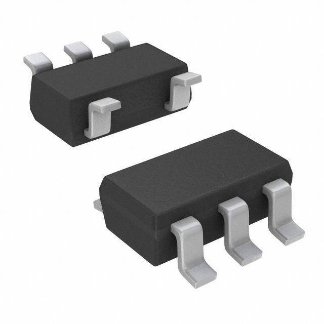
| 产品图片 |
|
| rohs | 符合RoHS无铅 / 符合限制有害物质指令(RoHS)规范要求 |
| 产品系列 | 逻辑集成电路,触发器,Texas Instruments SN74LVC1G79DCKR74LVC |
| 数据手册 | |
| 产品型号 | SN74LVC1G79DCKR |
| PCN设计/规格 | |
| 不同V、最大CL时的最大传播延迟 | 4.5ns @ 5V,50pF |
| 产品目录页面 | |
| 产品种类 | 触发器 |
| 传播延迟时间 | 5 ns |
| 低电平输出电流 | 32 mA |
| 元件数 | 1 |
| 其它名称 | 296-9850-2 |
| 功能 | 标准 |
| 包装 | 带卷 (TR) |
| 单位重量 | 2.500 mg |
| 商标 | Texas Instruments |
| 安装类型 | 表面贴装 |
| 安装风格 | SMD/SMT |
| 封装 | Reel |
| 封装/外壳 | 6-TSSOP(5 引线),SC-88A,SOT-353 |
| 封装/箱体 | SC-70-5 |
| 工作温度 | -40°C ~ 125°C |
| 工厂包装数量 | 3000 |
| 最大工作温度 | + 85 C |
| 最小工作温度 | - 40 C |
| 极性 | Non-Inverting |
| 标准包装 | 3,000 |
| 每元件位数 | 1 |
| 电压-电源 | 1.65 V ~ 5.5 V |
| 电流-输出高,低 | 32mA,32mA |
| 电流-静态 | 10µA |
| 电源电压-最大 | 5.5 V |
| 电源电压-最小 | 1.65 V |
| 电路数量 | 1 |
| 类型 | D 型 |
| 系列 | SN74LVC1G79 |
| 触发器类型 | 正边沿 |
| 输入电容 | 4pF |
| 输入类型 | Single-Ended |
| 输入线路数量 | 1 |
| 输出类型 | 非反相 |
| 输出线路数量 | 1 |
| 逻辑类型 | D-Type Flip-Flop |
| 逻辑系列 | 74LV |
| 频率-时钟 | 160MHz |
| 高电平输出电流 | - 32 mA |


- 商务部:美国ITC正式对集成电路等产品启动337调查
- 曝三星4nm工艺存在良率问题 高通将骁龙8 Gen1或转产台积电
- 太阳诱电将投资9.5亿元在常州建新厂生产MLCC 预计2023年完工
- 英特尔发布欧洲新工厂建设计划 深化IDM 2.0 战略
- 台积电先进制程称霸业界 有大客户加持明年业绩稳了
- 达到5530亿美元!SIA预计今年全球半导体销售额将创下新高
- 英特尔拟将自动驾驶子公司Mobileye上市 估值或超500亿美元
- 三星加码芯片和SET,合并消费电子和移动部门,撤换高东真等 CEO
- 三星电子宣布重大人事变动 还合并消费电子和移动部门
- 海关总署:前11个月进口集成电路产品价值2.52万亿元 增长14.8%


PDF Datasheet 数据手册内容提取
Product Order Technical Tools & Support & Folder Now Documents Software Community SN74LVC1G79 SCES220U–APRIL1999–REVISEDAPRIL2017 SN74LVC1G79 Single Positive-Edge-Triggered D-Type Flip-Flop 1 Features 3 Description • AvailableintheTexasInstruments The SN74LVC1G79 device is a single positive-edge- 1 triggered D-type flip-flop that is designed for 1.65-V to NanoFree™Package 5.5-VV operation. • Latch-UpPerformanceExceeds100mAPer CC JESD78,ClassII When data at the data (D) input meets the setup time requirement, the data is transferred to the Q output • ESDProtectionExceedsJESD22 on the positive-going edge of the clock pulse. Clock – 2000-VHuman-BodyModel(A114-A) triggering occurs at a voltage level and is not directly – 200-VMachineModel(A115-A) related to the rise time of the clock pulse. Following the hold-time interval, data at the D input can be – 1000-VCharged-DeviceModel(C101) changedwithoutaffectingthelevelattheoutput. • Supports5-VV Operation CC NanoFree™ package technology is a major • InputsAcceptVoltagesto5.5V breakthrough in IC packaging concepts, using the die • SupportsDownTranslationtoVCC asthepackage. • Maxt of6nsat3.3Vand50pFload pd This device is fully specified for partial-power-down • LowPowerConsumption,10-µAMaxICC applications using Ioff. The Ioff circuitry disables the • ±24-mAOutputDriveat3.3V outputs when the device is powered down. This inhibits current backflow into the device which • I supportsPartial-Power-DownModeandBack- off preventsdamagetothedevice. DriveProtection DeviceInformation(1) 2 Applications PARTNUMBER PACKAGE BODYSIZE • TestandMeasurement SN74LVC1G79DBV SOT-23(5) 2.90mm×1.60mm • EnterpriseSwitching SN74LVC1G79DCK SC70(5) 2.00mm×1.25mm • TelecomInfrastructure SN74LVC1G79DRL SOT(5) 1.60mm×1.20mm • PersonalElectronics SN74LVC1G79YZP DSBGA(5) 1.14mm×0.91mm • WhiteGoods (1) For all available packages, see the orderable addendum at theendofthedatasheet. LogicDiagram(PositiveLogic) 2 CLK C C C 4 TG Q C C C C 1 D TG TG TG C C C Copyright © 2017,Texas Instruments Incorporated 1 An IMPORTANT NOTICE at the end of this data sheet addresses availability, warranty, changes, use in safety-critical applications, intellectualpropertymattersandotherimportantdisclaimers.PRODUCTIONDATA.
SN74LVC1G79 SCES220U–APRIL1999–REVISEDAPRIL2017 www.ti.com Table of Contents 1 Features.................................................................. 1 8 DetailedDescription............................................ 11 2 Applications........................................................... 1 8.1 Overview.................................................................11 3 Description............................................................. 1 8.2 FunctionalBlockDiagram.......................................11 4 RevisionHistory..................................................... 2 8.3 FeatureDescription.................................................11 8.4 DeviceFunctionalModes........................................12 5 PinConfigurationandFunctions......................... 3 9 ApplicationandImplementation........................ 13 6 Specifications......................................................... 4 9.1 ApplicationInformation............................................13 6.1 AbsoluteMaximumRatings......................................4 9.2 TypicalApplication .................................................13 6.2 ESDRatings..............................................................4 10 PowerSupplyRecommendations..................... 14 6.3 RecommendedOperatingConditions.......................5 6.4 ThermalInformation..................................................5 11 Layout................................................................... 14 6.5 ElectricalCharacteristics...........................................6 11.1 LayoutGuidelines.................................................14 6.6 TimingRequirements:T =–40°Cto+85°C............6 11.2 LayoutExample....................................................14 A 6.7 TimingRequirements:T =–40°Cto+125°C..........6 12 DeviceandDocumentationSupport................. 15 A 6.8 SwitchingCharacteristics:C =15pF,T =–40°Cto 12.1 DocumentationSupport........................................15 L A +85°C......................................................................... 7 12.2 ReceivingNotificationofDocumentationUpdates15 6.9 SwitchingCharacteristics:CL=30or50pF,TA= 12.3 CommunityResources..........................................15 –40°Cto+85°C..........................................................7 12.4 Trademarks...........................................................15 6.10 SwitchingCharacteristics:C =30pFor50pF,T L A 12.5 ElectrostaticDischargeCaution............................15 =–40°Cto+125°C.....................................................7 12.6 Glossary................................................................15 6.11 OperatingCharacteristics........................................7 13 Mechanical,Packaging,andOrderable 6.12 TypicalCharacteristics............................................8 Information........................................................... 15 7 ParameterMeasurementInformation..................9 4 Revision History NOTE:Pagenumbersforpreviousrevisionsmaydifferfrompagenumbersinthecurrentversion. ChangesfromRevisionT(December2013)toRevisionU Page • AddedDeviceInformationtable,ESDRatingstable,ThermalInformationtable,FeatureDescriptionsection,Device FunctionalModes,ApplicationandImplementationsection,PowerSupplyRecommendationssection,Layout section,DeviceandDocumentationSupportsection,andMechanical,Packaging,andOrderableInformation section ................................................................................................................................................................................... 1 • ChangedthermalinformationtoalignwithJEDECstandards. ............................................................................................. 5 ChangesfromRevisionS(November2007)toRevisionT Page • UpdateddocumenttonewTIdatasheetformat.................................................................................................................... 1 • RemovedOrderingInformationtable..................................................................................................................................... 1 • UpdatedI inFeatures.......................................................................................................................................................... 1 off • Updatedoperatingtemperaturerange................................................................................................................................... 5 • AddedESDwarning............................................................................................................................................................. 15 2 SubmitDocumentationFeedback Copyright©1999–2017,TexasInstrumentsIncorporated ProductFolderLinks:SN74LVC1G79
SN74LVC1G79 www.ti.com SCES220U–APRIL1999–REVISEDAPRIL2017 5 Pin Configuration and Functions DBVPackage 5-PinSOT-23 DRLPackage TopView 5-PinSOT TopView D 1 5 V CC CLK 2 GND 3 4 Q YZPPackage 5-PinDSBGA DCKPackage BottomView 5-PinSC70 1 2 TopView C GND Q D 1 5 V CC CLK 2 B CLK GND 3 4 Q A D VCC Seemechanicaldrawingsfordimensions. Not to scale PinFunctions PIN DBV,DCK, I/O DESCRIPTION NAME YZP DRL D 1 A1 I Datainput CLK 2 B1 I Positive-Edge-TriggeredClockinput GND 3 C1 — Ground Q 4 C2 O Non-invertedoutput V 5 A2 — PositiveSupply CC Copyright©1999–2017,TexasInstrumentsIncorporated SubmitDocumentationFeedback 3 ProductFolderLinks:SN74LVC1G79
SN74LVC1G79 SCES220U–APRIL1999–REVISEDAPRIL2017 www.ti.com 6 Specifications 6.1 Absolute Maximum Ratings overoperatingfree-airtemperaturerange(unlessotherwisenoted)(1) MIN MAX UNIT V Supplyvoltage –0.5 6.5 V CC V Inputvoltage(2) –0.5 6.5 V I V Voltagerangeappliedtoanyoutputinthehigh-impedanceorpower-offstate(2) –0.5 6.5 V O V Voltagerangeappliedtoanyoutputinthehighorlowstate(2)(3) –0.5 V +0.5 V O CC I Inputclampcurrent V <0 –50 mA IK I I Outputclampcurrent V <0 –50 mA OK O I Continuousoutputcurrent ±50 mA O ContinuouscurrentthroughV orGND ±100 mA CC T Storagetemperature –65 150 °C stg T Junctiontemperature 150 °C J (1) StressesbeyondthoselistedunderAbsoluteMaximumRatingsmaycausepermanentdamagetothedevice.Thesearestressratings only,andfunctionaloperationofthedeviceattheseoranyotherconditionsbeyondthoseindicatedunderRecommendedOperating Conditionsisnotimplied.Exposuretoabsolute-maximum-ratedconditionsforextendedperiodsmayaffectdevicereliability. (2) Theinputnegative-voltageandoutputvoltageratingsmaybeexceedediftheinputandoutputcurrentratingsareobserved. (3) ThevalueofV isprovidedintheRecommendedOperatingConditionstable. CC 6.2 ESD Ratings VALUE UNIT Humanbodymodel(HBM),perANSI/ESDA/JEDECJS-001(1) ±2000 V Electrostatic Chargeddevicemodel(CDM),perJEDECspecificationJESD22-C101(2) ±1000 V (ESD) discharge MachineModel(MM),A115-A 200 (1) JEDECdocumentJEP155statesthat500-VHBMallowssafemanufacturingwithastandardESDcontrolprocess. (2) JEDECdocumentJEP157statesthat250-VCDMallowssafemanufacturingwithastandardESDcontrolprocess. 4 SubmitDocumentationFeedback Copyright©1999–2017,TexasInstrumentsIncorporated ProductFolderLinks:SN74LVC1G79
SN74LVC1G79 www.ti.com SCES220U–APRIL1999–REVISEDAPRIL2017 6.3 Recommended Operating Conditions overoperatingfree-airtemperaturerange(unlessotherwisenoted)(1) MIN MAX UNIT Operating 1.65 5.5 VCC Supplyvoltage V Dataretentiononly 1.5 VCC=1.65Vto1.95V 0.65×VCC VCC=2.3Vto2.7V 1.7 VIH High-levelinputvoltage V VCC=3Vto3.6V 2 VCC=4.5Vto5.5V 0.7×VCC VCC=1.65Vto1.95V 0.35×VCC VCC=2.3Vto2.7V 0.7 VIL Low-levelinputvoltage V VCC=3Vto3.6V 0.8 VCC=4.5Vto5.5V 0.3×VCC VI Inputvoltage 0 5.5 V VO Outputvoltage 0 VCC V VCC=1.65V –4 VCC=2.3V –8 IOH High-leveloutputcurrent –16 mA VCC=3V –24 VCC=4.5V –32 VCC=1.65V 4 VCC=2.3V 8 IOL Low-leveloutputcurrent 16 mA VCC=3V 24 VCC=4.5V 32 VCC=1.8V±0.15V,2.5V±0.2V 20 Δt/Δv Inputtransitionriseorfallrate VCC=3.3V±0.3V 10 ns/V VCC=5V±0.5V 5 TA Operatingfree-airtemperature –40 125 °C (1) AllunusedinputsofthedevicemustbeheldatV orGNDtoensureproperdeviceoperation.SeeImplicationsofSloworFloating CC CMOSInputs,SCBA004. 6.4 Thermal Information SN74LVC1G79 THERMALMETRIC(1) DBV(SOT-23) DCK(SC70) DRL(SOT) YZP(DSBGA) UNIT 5PINS 5PINS 5PINS 5PINS R Junction-to-ambientthermalresistance 247.2 277.6 294.3 144.4 °C/W θJA R Junction-to-case(top)thermalresistance 154.5 179.5 129.9 1.3 °C/W θJC(top) R Junction-to-boardthermalresistance 86.8 75.9 143.4 39.9 °C/W θJB ψ Junction-to-topcharacterizationparameter 58.0 49.7 14.3 0.5 °C/W JT Junction-to-boardcharacterization ψ 86.4 75.1 144.0 39.7 °C/W JB parameter (1) Formoreinformationabouttraditionalandnewthermalmetrics,seetheSemiconductorandICPackageThermalMetricsapplication report. Copyright©1999–2017,TexasInstrumentsIncorporated SubmitDocumentationFeedback 5 ProductFolderLinks:SN74LVC1G79
SN74LVC1G79 SCES220U–APRIL1999–REVISEDAPRIL2017 www.ti.com 6.5 Electrical Characteristics overrecommendedoperatingfree-airtemperaturerange(unlessotherwisenoted) TA=–40°Cto+85°C TA=–40°Cto+125°C PARAMETER TESTCONDITIONS VCC MIN TYP(1) MAX MIN TYP(1) MAX UNIT IOH=–100µA 1.65Vto5.5V VCC–0.1 VCC–0.1 IOH=–4mA 1.65V 1.2 1.2 IOH=–8mA 2.3V 1.9 1.9 VOH V IOH=–16mA 2.4 2.4 3V IOH=–24mA 2.3 2.3 IOH=–32mA 4.5V 3.8 3.8 IOL=100µA 1.65Vto5.5V 0.1 0.1 IOL=4mA 1.65V 0.45 0.45 IOL=8mA 2.3V 0.3 0.3 VOL V IOL=16mA 0.4 0.4 3V IOL=24mA 0.55 0.55 IOL=32mA 4.5V 0.55 0.55 II Allinputs VI=5.5VorGND 0to5.5V ±10 ±5 µA Ioff VIorVO=5.5V 0 ±10 ±10 µA ICC VI=5.5VorGND, IO=0 1.65Vto5.5V 10 10 µA ΔICC OOntheerinipnuptuatstaVtCVCC–C0o.r6GVN,D 3Vto5.5V 500 500 µA Ci VI=VCCorGND 3.3V 4 4 pF (1) AlltypicalvaluesareatV =3.3V,T =25°C. CC A 6.6 Timing Requirements: T = –40°C to +85°C A overoperatingfree-airtemperaturerange(unlessotherwisenoted)(seeFigure3) TA=–40°Cto+85°C PARAMETER VCC=1.8 VCC=2.5 VCC=3.3V VCC=5V UNIT ±0.15V ±0.2V ±0.3V ±0.5V MIN MAX MIN MAX MIN MAX MIN MAX fclock Clockfrequency 160 160 160 160 MHz tw Pulseduration,CLKhighorlow 2.5 2.5 2.5 2.5 ns Datahigh 2.2 1.4 1.3 1.2 tsu SetuptimebeforeCLK↑ ns Datalow 2.6 1.4 1.3 1.2 th Holdtime,dataafterCLK↑ 0.3 0.4 1 0.5 ns 6.7 Timing Requirements: T = –40°C to +125°C A overoperatingfree-airtemperaturerange(unlessotherwisenoted)(seeFigure3) TA=–40°Cto+125°C PARAMETER VCC=1.8 VCC=2.5 VCC=3.3V VCC=5V UNIT ±0.15V ±0.2V ±0.3V ±0.5V MIN MAX MIN MAX MIN MAX MIN MAX fclock Clockfrequency 160 160 160 160 MHz tw Pulseduration,CLKhighorlow 2.5 2.5 2.5 2.5 ns Datahigh 2.2 1.4 1.3 1.2 tsu SetuptimebeforeCLK↑ ns Datalow 2.6 1.4 1.3 1.2 th Holdtime,dataafterCLK↑ 0.3 0.4 1 0.5 ns 6 SubmitDocumentationFeedback Copyright©1999–2017,TexasInstrumentsIncorporated ProductFolderLinks:SN74LVC1G79
SN74LVC1G79 www.ti.com SCES220U–APRIL1999–REVISEDAPRIL2017 6.8 Switching Characteristics: C = 15 pF, T = –40°C to +85°C L A overrecommendedoperatingfree-airtemperaturerange,C =15pF(unlessotherwisenoted)(seeFigure3) L TA=–40°Cto+85°C PARAMETER FROM TO VCC=1.8V VCC=2.5V VCC=3.3V VCC=5V UNIT (INPUT) (OUTPUT) ±0.15V ±0.2V ±0.3V ±0.5V MIN MAX MIN MAX MIN MAX MIN MAX fmax 160 160 160 160 MHz tpd CLK Q 2.5 9.1 1.2 6 1 4 0.8 3.8 ns 6.9 Switching Characteristics: C = 30 or 50 pF, T = –40°C to +85°C L A overrecommendedoperatingfree-airtemperaturerange,C =30pFor50pF(unlessotherwisenoted)(seeFigure4) L TA=–40°Cto+85°C PARAMETER FROM TO VCC=1.8V VCC=2.5V VCC=3.3V VCC=5V UNIT (INPUT) (OUTPUT) ±0.15V ±0.2V ±0.3V ±0.5V MIN MAX MIN MAX MIN MAX MIN MAX fmax 160 160 160 160 MHz tpd CLK Q 3.9 9.9 2 7 1.7 5 1 4.5 ns 6.10 Switching Characteristics: C = 30 pF or 50 pF, T = –40°C to +125°C L A overrecommendedoperatingfree-airtemperaturerange,C =30pFor50pF(unlessotherwisenoted)(seeFigure4) L TA=–40°Cto+125°C PARAMETER FROM TO VCC=1.8V VCC=2.5V VCC=3.3V VCC=5V UNIT (INPUT) (OUTPUT) ±0.15V ±0.2V ±0.3V ±0.5V MIN MAX MIN MAX MIN MAX MIN MAX fmax 160 160 160 160 MHz tpd CLK Q 3.9 12 2 8.5 1.7 6 1 5 ns 6.11 Operating Characteristics T =25°C A TEST VCC=1.8V VCC=2.5V VCC=3.3V VCC=5V PARAMETER UNIT CONDITIONS TYP TYP TYP TYP Cpd Powerdissipationcapacitance f=10MHz 26 26 27 30 pF Copyright©1999–2017,TexasInstrumentsIncorporated SubmitDocumentationFeedback 7 ProductFolderLinks:SN74LVC1G79
SN74LVC1G79 SCES220U–APRIL1999–REVISEDAPRIL2017 www.ti.com 6.12 Typical Characteristics ThisplotshowsthedifferentI valuesforvariousvoltagesonthedatainput(D).Voltagesweepontheinputisfrom0Vto CC 6.5V. 2 20 VCC = 1.8 V VCC = 3.3 V 1.8 VCC = 2.5 V 18 VCC = 5.0 V 1.6 16 A] A] m 1.4 m 14 [C [C C 1.2 C 12 nt I nt I e 1 e 10 urr urr C 0.8 C 8 y y ppl 0.6 ppl 6 u u S S 0.4 4 0.2 2 0 0 0 0.5 1 1.5 2 2.5 3 3.5 4 4.5 5 5.5 6 6.5 0 0.5 1 1.5 2 2.5 3 3.5 4 4.5 5 5.5 6 6.5 Data (D) Input Voltage [V] Data (D) Input Voltage [V] ICCv ICCv VCC=1.8V VCC=2.5V VCC=3.3V VCC=5V Figure1.SupplyCurrent(I )vsData(D)InputVoltage Figure2.SupplyCurrent(I )vsData(D)InputVoltage CC CC 8 SubmitDocumentationFeedback Copyright©1999–2017,TexasInstrumentsIncorporated ProductFolderLinks:SN74LVC1G79
SN74LVC1G79 www.ti.com SCES220U–APRIL1999–REVISEDAPRIL2017 7 Parameter Measurement Information V LOAD R S1 Open From Output L TEST S1 Under Test GND t /t Open C PLH PHL (see NoteA)L RL tPLZ/tPZL VLOAD t /t GND PHZ PZH LOAD CIRCUIT INPUTS V V V C R V CC V t/t M LOAD L L D I r f 1.8 V±0.15 V V £2 ns V /2 2 ×V 15 pF 1 MW 0.15 V CC CC CC 2.5 V±0.2 V V £2 ns V /2 2 ×V 15 pF 1 MW 0.15 V CC CC CC 3.3 V±0.3 V 3 V £2.5 ns 1.5 V 6 V 15 pF 1 MW 0.3 V 5 V±0.5 V V £2.5 ns V /2 2 ×V 15 pF 1 MW 0.3 V CC CC CC V I Timing Input V M 0 V t W VI tsu th V Input V V I M M Data Input V V M M 0 V 0 V VOLTAGE WAVEFORMS VOLTAGE WAVEFORMS PULSE DURATION SETUPAND HOLD TIMES Input VM VM VI COounttpruotl VM VM VI 0 V 0 V t t t t PLH PHL PZL PLZ V Output V /2 Output VM VM OH WSav1e afot rVm 1 VM V + V LOAD VOL (see NoteL OBAD) OL D VOL t t PHL PLH t t PZH PHZ Output VM VM VOH WSa1v eaOfto uGrtmpNu D2t VM VOH–VD VOH VOL (see Note B) »0 V VOLTAGE WAVEFORMS VOLTAGE WAVEFORMS PROPAGATION DELAYTIMES ENABLEAND DISABLE TIMES INVERTINGAND NONINVERTING OUTPUTS LOW-AND HIGH-LEVELENABLING NOTES: A. C includes probe and jig capacitance. L B. Waveform 1 is for an output with internal conditions such that the output is low, except when disabled by the output control. Waveform 2 is for an output with internal conditions such that the output is high, except when disabled by the output control. C. All input pulses are supplied by generators having the following characteristics: PRR£10 MHz, Z = 50W. O D. The outputs are measured one at a time, with one transition per measurement. E. t and t are the same as t . PLZ PHZ dis F. t and t are the same as t . PZL PZH en G.t and t are the same as t . PLH PHL pd H. All parameters and waveforms are not applicable to all devices. Figure3. LoadCircuitandVoltageWaveforms Copyright©1999–2017,TexasInstrumentsIncorporated SubmitDocumentationFeedback 9 ProductFolderLinks:SN74LVC1G79
SN74LVC1G79 SCES220U–APRIL1999–REVISEDAPRIL2017 www.ti.com Parameter Measurement Information (continued) V LOAD R S1 Open From Output L TEST S1 Under Test GND t /t Open C PLH PHL (see NoteA)L RL tPLZ/tPZL VLOAD t /t GND PHZ PZH LOAD CIRCUIT INPUTS V V V C R V CC V t/t M LOAD L L D I r f 1.8 V±0.15 V V £2 ns V /2 2 ×V 30 pF 1 kW 0.15 V CC CC CC 2.5 V±0.2 V V £2 ns V /2 2 ×V 30 pF 500W 0.15 V CC CC CC 3.3 V±0.3 V 3 V £2.5 ns 1.5 V 6 V 50 pF 500W 0.3 V 5 V±0.5 V V £2.5 ns V /2 2 ×V 50 pF 500W 0.3 V CC CC CC V I Timing Input V M 0 V t W VI tsu th V Input V V I M M Data Input V V M M 0 V 0 V VOLTAGE WAVEFORMS VOLTAGE WAVEFORMS PULSE DURATION SETUPAND HOLD TIMES Input VM VM VI COounttpruotl VM VM VI 0 V 0 V t t t t PLH PHL PZL PLZ V Output V /2 Output VM VM OH WSav1e afot rVm 1 VM V + V LOAD VOL (see NoteL OBAD) OL D VOL t t PHL PLH t t PZH PHZ Output VM VM VOH WSa1v eaOfto uGrtmpNu D2t VM VOH–VD VOH VOL (see Note B) »0 V VOLTAGE WAVEFORMS VOLTAGE WAVEFORMS PROPAGATION DELAYTIMES ENABLEAND DISABLE TIMES INVERTINGAND NONINVERTING OUTPUTS LOW-AND HIGH-LEVELENABLING NOTES: A. C includes probe and jig capacitance. L B. Waveform 1 is for an output with internal conditions such that the output is low, except when disabled by the output control. Waveform 2 is for an output with internal conditions such that the output is high, except when disabled by the output control. C. All input pulses are supplied by generators having the following characteristics: PRR£10 MHz, Z = 50W. O D. The outputs are measured one at a time, with one transition per measurement. E. t and t are the same as t . PLZ PHZ dis F. t and t are the same as t . PZL PZH en G.t and t are the same as t . PLH PHL pd H. All parameters and waveforms are not applicable to all devices. Figure4. LoadCircuitandVoltageWaveforms 10 SubmitDocumentationFeedback Copyright©1999–2017,TexasInstrumentsIncorporated ProductFolderLinks:SN74LVC1G79
SN74LVC1G79 www.ti.com SCES220U–APRIL1999–REVISEDAPRIL2017 8 Detailed Description 8.1 Overview The SN74LVC1G79 is a single positive-edge-triggered D-type flip-flop. Data at the input (D) is transferred to the output (Q) on the positive-going edge of the clock pulse when the setup time requirement is met. Because the clock triggering occurs at a voltage level, it is not directly related to the rise time of the clock pulse. This allows fordataattheinputtobechangedwithoutaffectingthelevelattheoutput,followingthehold-timeinterval. 8.2 Functional Block Diagram 2 CLK C C C 4 TG Q C C C C 1 D TG TG TG C C C Copyright © 2017,Texas Instruments Incorporated Figure5. LogicDiagram(PositiveLogic) 8.3 Feature Description 8.3.1 BalancedHigh-DriveCMOSPush-PullOutputs A balanced output allows the device to sink and source similar currents. The high drive capability of this device creates fast edges into light loads so routing and load conditions should be considered to prevent ringing. Additionally, the outputs of this device are capable of driving larger currents than the device can sustain without being damaged. It is important for the power output of the device to be limited to avoid thermal runaway and damage due to over-current. The electrical and thermal limits defined the in the Absolute Maximum Ratings must befollowedatalltimes. 8.3.2 StandardCMOSInputs Standard CMOS inputs are high impedance and are typically modeled as a resistor in parallel with the input capacitance given in the Electrical Characteristics. The worst case resistance is calculated with the maximum input voltage, given in the Recommended Operating Conditions, and the maximum input leakage current, given intheElectricalCharacteristics,usingohm'slaw(R=V ÷ I). Signals applied to the inputs need to have fast edge rates, as defined by Δt/Δv in Recommended Operating Conditions to avoid excessive currents and oscillations. If tolerance to a slow or noisy input signal is required, a device with a Schmitt-trigger input should be utilized to condition the input signal prior to the standard CMOS input. Copyright©1999–2017,TexasInstrumentsIncorporated SubmitDocumentationFeedback 11 ProductFolderLinks:SN74LVC1G79
SN74LVC1G79 SCES220U–APRIL1999–REVISEDAPRIL2017 www.ti.com Feature Description (continued) 8.3.3 ClampDiodes Theinputsandoutputstothisdevicehavenegativeclampingdiodes. CAUTION Voltages beyond the values specified in the Absolute Maximum Ratings table can cause damage to the device. The input negative-voltage and output voltage ratings maybeexceedediftheinputandoutputclamp-currentratingsareobserved. V Device CC Input Logic Output -IIK -IOK GND Figure6. ElectricalPlacementofClampingDiodesforEachInputandOutput 8.3.4 PartialPowerDown(I ) off The inputs and outputs for this device enter a high impedance state when the supply voltage is 0 V. The maximum leakage into or out of any input or output pin on the device is specified by I in the Electrical off Characteristics. 8.3.5 Over-VoltageTolerantInputs Input signals to this device can be driven above the supply voltage so long as they remain below the maximum inputvoltagevaluespecifiedintheAbsoluteMaximumRatings. 8.4 Device Functional Modes Table1liststhefunctionalmodesofSN74LVC1G79. Table1.FunctionTable INPUTS OUTPUT CLK D Y ↑ H H ↑ L L L X Q 0 12 SubmitDocumentationFeedback Copyright©1999–2017,TexasInstrumentsIncorporated ProductFolderLinks:SN74LVC1G79
SN74LVC1G79 www.ti.com SCES220U–APRIL1999–REVISEDAPRIL2017 9 Application and Implementation NOTE Information in the following applications sections is not part of the TI component specification, and TI does not warrant its accuracy or completeness. TI’s customers are responsible for determining suitability of components for their purposes. Customers should validateandtesttheirdesignimplementationtoconfirmsystemfunctionality. 9.1 Application Information A useful application for the SN74LVC1G79 is using it as a data latch with low-voltage data retention. This application implements the use of a microcontroller GPIO pin to act as a clock to set the output state and a second GPIO to provide the input data. If the SN74LVC1G79 is being powered from 1.8 V and there is concern that a power glitch could exist as low as 1.5 V, the device will retain the state of the Q output. An example of this data retention is shown in Figure 8 where the V drops to 1.5 V and the Q output maintains the HIGH output CC statewhenV returnsto1.8V.IftheV voltagedropsbelow1.5V,dataretentionisnotguaranteed. CC CC 9.2 Typical Application V > 1.65V for Operation CC V > 1.50V for Data Retention CC GPIO 1 D VCC 5 MCU SN74LVC1G79 2 CLK CLK 3 GND Q 4 Copyright © 2017, Texas Instruments Incorporated Figure7. LowVoltageDataRetentionWithSN74LVC1G79 9.2.1 DesignRequirements The SN74LVC1G79 device uses CMOS technology and has balanced output drive. Take care to avoid bus contentionbecauseitcandrivecurrentsthatwouldexceedmaximumlimits. 9.2.2 DetailedDesignProcedure 1. Recommendedinputconditions: – Forrisetimeandfalltimespecifications,see Δt/ΔvinRecommendedOperatingConditions. – Forspecifiedhighandlowlevels,seeV andV inRecommendedOperatingConditions. IH IL – Input voltages are recommended to not go below 0 V and not exceed 5.5 V for any V . See CC RecommendedOperatingConditions. 2. Recommendedoutputconditions: – Loadcurrentsshouldnotexceed ±50mA.SeeAbsoluteMaximumRatings. – Output voltages are recommended to not go below 0 V and not exceed the V voltage. See CC RecommendedOperatingConditions. Copyright©1999–2017,TexasInstrumentsIncorporated SubmitDocumentationFeedback 13 ProductFolderLinks:SN74LVC1G79
SN74LVC1G79 SCES220U–APRIL1999–REVISEDAPRIL2017 www.ti.com Typical Application (continued) 9.2.3 ApplicationCurve Positive Supply Voltage (V ) CC NNoonn--iinnvveerrtteedd OOuuttppuutt ((QQ)) Figure8. DataRetentionWithV GlitchDownto1.5V CC 10 Power Supply Recommendations The power supply can be any voltage between the minimum and maximum supply voltage rating listed in RecommendedOperatingConditions.A0.1-µFbypasscapacitorisrecommendedtobeconnectedfromtheVCC terminal to GND to prevent power disturbance. To reject different frequencies of noise, use multiple bypass capacitors in parallel. Capacitors with values of 0.1 µF and 1 µF are commonly used in parallel. The bypass capacitormustbeinstalledasclosetothepowerterminalaspossibleforbestresults. 11 Layout 11.1 Layout Guidelines When a PCB trace turns a corner at a 90° angle, a reflection can occur. A reflection occurs primarily because of the change of width of the trace. At the apex of the turn, the trace width increases to 1.414 times the width. This increase upsets the transmission-line characteristics, especially the distributed capacitance and self–inductance of the trace which results in the reflection. Not all PCB traces can be straight and therefore some traces must turn corners. Figure 9 shows progressively better techniques of rounding corners. Only the last example (BEST) maintainsconstanttracewidthandminimizesreflections. 11.2 Layout Example WORST BETTER BEST W 2 1W min. W Figure9. TraceExample 14 SubmitDocumentationFeedback Copyright©1999–2017,TexasInstrumentsIncorporated ProductFolderLinks:SN74LVC1G79
SN74LVC1G79 www.ti.com SCES220U–APRIL1999–REVISEDAPRIL2017 12 Device and Documentation Support 12.1 Documentation Support 12.1.1 RelatedDocumentation Forrelateddocumentationseethefollowing: • ImplicationsofSloworFloatingCMOSInputs,SCBA004 • UnderstandingandInterpretingStandardLogicDataSheets,SZZA036 • Power-UpBehaviorofClockedDevices,SCHA005 12.2 Receiving Notification of Documentation Updates To receive notification of documentation updates, navigate to the device product folder on ti.com. In the upper right corner, click on Alert me to register and receive a weekly digest of any product information that has changed.Forchangedetails,reviewtherevisionhistoryincludedinanyreviseddocument. 12.3 Community Resources The following links connect to TI community resources. Linked contents are provided "AS IS" by the respective contributors. They do not constitute TI specifications and do not necessarily reflect TI's views; see TI's Terms of Use. TIE2E™OnlineCommunity TI'sEngineer-to-Engineer(E2E)Community.Createdtofostercollaboration amongengineers.Ate2e.ti.com,youcanaskquestions,shareknowledge,exploreideasandhelp solveproblemswithfellowengineers. DesignSupport TI'sDesignSupport QuicklyfindhelpfulE2Eforumsalongwithdesignsupporttoolsand contactinformationfortechnicalsupport. 12.4 Trademarks NanoFree,E2EaretrademarksofTexasInstruments. Allothertrademarksarethepropertyoftheirrespectiveowners. 12.5 Electrostatic Discharge Caution Thesedeviceshavelimitedbuilt-inESDprotection.Theleadsshouldbeshortedtogetherorthedeviceplacedinconductivefoam duringstorageorhandlingtopreventelectrostaticdamagetotheMOSgates. 12.6 Glossary SLYZ022—TIGlossary. Thisglossarylistsandexplainsterms,acronyms,anddefinitions. 13 Mechanical, Packaging, and Orderable Information The following pages include mechanical packaging and orderable information. This information is the most current data available for the designated devices. This data is subject to change without notice and revision of thisdocument.Forbrowserbasedversionsofthisdatasheet,refertothelefthandnavigation. Copyright©1999–2017,TexasInstrumentsIncorporated SubmitDocumentationFeedback 15 ProductFolderLinks:SN74LVC1G79
PACKAGE OPTION ADDENDUM www.ti.com 6-Feb-2020 PACKAGING INFORMATION Orderable Device Status Package Type Package Pins Package Eco Plan Lead/Ball Finish MSL Peak Temp Op Temp (°C) Device Marking Samples (1) Drawing Qty (2) (6) (3) (4/5) SN74LVC1G79DBVR ACTIVE SOT-23 DBV 5 3000 Green (RoHS NIPDAU | SN Level-1-260C-UNLIM -40 to 125 (C795, C79F, C79J, & no Sb/Br) C79R) SN74LVC1G79DBVT ACTIVE SOT-23 DBV 5 250 Green (RoHS NIPDAU | SN Level-1-260C-UNLIM -40 to 125 (C795, C79F, C79J, & no Sb/Br) C79R) SN74LVC1G79DBVTG4 ACTIVE SOT-23 DBV 5 250 Green (RoHS NIPDAU Level-1-260C-UNLIM -40 to 125 C79F & no Sb/Br) SN74LVC1G79DCKR ACTIVE SC70 DCK 5 3000 Green (RoHS NIPDAU | SN Level-1-260C-UNLIM -40 to 125 (CR5, CRF, CRJ, CR & no Sb/Br) R) SN74LVC1G79DCKRE4 ACTIVE SC70 DCK 5 3000 Green (RoHS NIPDAU Level-1-260C-UNLIM -40 to 125 CR5 & no Sb/Br) SN74LVC1G79DCKRG4 ACTIVE SC70 DCK 5 3000 Green (RoHS NIPDAU Level-1-260C-UNLIM -40 to 125 CR5 & no Sb/Br) SN74LVC1G79DCKT ACTIVE SC70 DCK 5 250 Green (RoHS NIPDAU | SN Level-1-260C-UNLIM -40 to 125 (CR5, CRF, CRJ, CR & no Sb/Br) R) SN74LVC1G79DCKTG4 ACTIVE SC70 DCK 5 250 Green (RoHS NIPDAU Level-1-260C-UNLIM -40 to 125 CR5 & no Sb/Br) SN74LVC1G79DRLR ACTIVE SOT-5X3 DRL 5 4000 Green (RoHS NIPDAU | NIPDAUAG Level-1-260C-UNLIM -40 to 125 (CR7, CRR) & no Sb/Br) SN74LVC1G79YZPR ACTIVE DSBGA YZP 5 3000 Green (RoHS SNAGCU Level-1-260C-UNLIM -40 to 85 (CR7, CRN) & no Sb/Br) (1) The marketing status values are defined as follows: ACTIVE: Product device recommended for new designs. LIFEBUY: TI has announced that the device will be discontinued, and a lifetime-buy period is in effect. NRND: Not recommended for new designs. Device is in production to support existing customers, but TI does not recommend using this part in a new design. PREVIEW: Device has been announced but is not in production. Samples may or may not be available. OBSOLETE: TI has discontinued the production of the device. (2) RoHS: TI defines "RoHS" to mean semiconductor products that are compliant with the current EU RoHS requirements for all 10 RoHS substances, including the requirement that RoHS substance do not exceed 0.1% by weight in homogeneous materials. Where designed to be soldered at high temperatures, "RoHS" products are suitable for use in specified lead-free processes. TI may reference these types of products as "Pb-Free". RoHS Exempt: TI defines "RoHS Exempt" to mean products that contain lead but are compliant with EU RoHS pursuant to a specific EU RoHS exemption. Green: TI defines "Green" to mean the content of Chlorine (Cl) and Bromine (Br) based flame retardants meet JS709B low halogen requirements of <=1000ppm threshold. Antimony trioxide based flame retardants must also meet the <=1000ppm threshold requirement. (3) MSL, Peak Temp. - The Moisture Sensitivity Level rating according to the JEDEC industry standard classifications, and peak solder temperature. Addendum-Page 1
PACKAGE OPTION ADDENDUM www.ti.com 6-Feb-2020 (4) There may be additional marking, which relates to the logo, the lot trace code information, or the environmental category on the device. (5) Multiple Device Markings will be inside parentheses. Only one Device Marking contained in parentheses and separated by a "~" will appear on a device. If a line is indented then it is a continuation of the previous line and the two combined represent the entire Device Marking for that device. (6) Lead/Ball Finish - Orderable Devices may have multiple material finish options. Finish options are separated by a vertical ruled line. Lead/Ball Finish values may wrap to two lines if the finish value exceeds the maximum column width. Important Information and Disclaimer:The information provided on this page represents TI's knowledge and belief as of the date that it is provided. TI bases its knowledge and belief on information provided by third parties, and makes no representation or warranty as to the accuracy of such information. Efforts are underway to better integrate information from third parties. TI has taken and continues to take reasonable steps to provide representative and accurate information but may not have conducted destructive testing or chemical analysis on incoming materials and chemicals. TI and TI suppliers consider certain information to be proprietary, and thus CAS numbers and other limited information may not be available for release. In no event shall TI's liability arising out of such information exceed the total purchase price of the TI part(s) at issue in this document sold by TI to Customer on an annual basis. OTHER QUALIFIED VERSIONS OF SN74LVC1G79 : •Automotive: SN74LVC1G79-Q1 •Enhanced Product: SN74LVC1G79-EP NOTE: Qualified Version Definitions: •Automotive - Q100 devices qualified for high-reliability automotive applications targeting zero defects •Enhanced Product - Supports Defense, Aerospace and Medical Applications Addendum-Page 2
PACKAGE MATERIALS INFORMATION www.ti.com 4-Jun-2020 TAPE AND REEL INFORMATION *Alldimensionsarenominal Device Package Package Pins SPQ Reel Reel A0 B0 K0 P1 W Pin1 Type Drawing Diameter Width (mm) (mm) (mm) (mm) (mm) Quadrant (mm) W1(mm) SN74LVC1G79DBVR SOT-23 DBV 5 3000 178.0 9.0 3.3 3.2 1.4 4.0 8.0 Q3 SN74LVC1G79DBVR SOT-23 DBV 5 3000 178.0 9.0 3.23 3.17 1.37 4.0 8.0 Q3 SN74LVC1G79DBVR SOT-23 DBV 5 3000 180.0 8.4 3.23 3.17 1.37 4.0 8.0 Q3 SN74LVC1G79DBVR SOT-23 DBV 5 3000 178.0 9.2 3.3 3.23 1.55 4.0 8.0 Q3 SN74LVC1G79DBVT SOT-23 DBV 5 250 178.0 9.0 3.3 3.2 1.4 4.0 8.0 Q3 SN74LVC1G79DBVT SOT-23 DBV 5 250 180.0 8.4 3.23 3.17 1.37 4.0 8.0 Q3 SN74LVC1G79DBVT SOT-23 DBV 5 250 178.0 9.2 3.3 3.23 1.55 4.0 8.0 Q3 SN74LVC1G79DBVT SOT-23 DBV 5 250 178.0 9.0 3.3 3.2 1.4 4.0 8.0 Q3 SN74LVC1G79DCKR SC70 DCK 5 3000 180.0 8.4 2.47 2.3 1.25 4.0 8.0 Q3 SN74LVC1G79DCKR SC70 DCK 5 3000 178.0 9.0 2.4 2.5 1.2 4.0 8.0 Q3 SN74LVC1G79DCKR SC70 DCK 5 3000 178.0 9.2 2.4 2.4 1.22 4.0 8.0 Q3 SN74LVC1G79DCKR SC70 DCK 5 3000 178.0 9.0 2.4 2.5 1.2 4.0 8.0 Q3 SN74LVC1G79DCKRG4 SC70 DCK 5 3000 178.0 9.2 2.4 2.4 1.22 4.0 8.0 Q3 SN74LVC1G79DCKT SC70 DCK 5 250 178.0 9.2 2.4 2.4 1.22 4.0 8.0 Q3 SN74LVC1G79DCKT SC70 DCK 5 250 178.0 9.0 2.4 2.5 1.2 4.0 8.0 Q3 SN74LVC1G79DCKT SC70 DCK 5 250 178.0 9.0 2.4 2.5 1.2 4.0 8.0 Q3 SN74LVC1G79DCKTG4 SC70 DCK 5 250 178.0 9.2 2.4 2.4 1.22 4.0 8.0 Q3 SN74LVC1G79DRLR SOT-5X3 DRL 5 4000 180.0 8.4 1.98 1.78 0.69 4.0 8.0 Q3 PackMaterials-Page1
PACKAGE MATERIALS INFORMATION www.ti.com 4-Jun-2020 Device Package Package Pins SPQ Reel Reel A0 B0 K0 P1 W Pin1 Type Drawing Diameter Width (mm) (mm) (mm) (mm) (mm) Quadrant (mm) W1(mm) SN74LVC1G79DRLR SOT-5X3 DRL 5 4000 180.0 9.5 1.78 1.78 0.69 4.0 8.0 Q3 SN74LVC1G79YZPR DSBGA YZP 5 3000 178.0 9.2 1.02 1.52 0.63 4.0 8.0 Q1 *Alldimensionsarenominal Device PackageType PackageDrawing Pins SPQ Length(mm) Width(mm) Height(mm) SN74LVC1G79DBVR SOT-23 DBV 5 3000 180.0 180.0 18.0 SN74LVC1G79DBVR SOT-23 DBV 5 3000 180.0 180.0 18.0 SN74LVC1G79DBVR SOT-23 DBV 5 3000 202.0 201.0 28.0 SN74LVC1G79DBVR SOT-23 DBV 5 3000 180.0 180.0 18.0 SN74LVC1G79DBVT SOT-23 DBV 5 250 180.0 180.0 18.0 SN74LVC1G79DBVT SOT-23 DBV 5 250 202.0 201.0 28.0 SN74LVC1G79DBVT SOT-23 DBV 5 250 180.0 180.0 18.0 SN74LVC1G79DBVT SOT-23 DBV 5 250 180.0 180.0 18.0 SN74LVC1G79DCKR SC70 DCK 5 3000 202.0 201.0 28.0 SN74LVC1G79DCKR SC70 DCK 5 3000 180.0 180.0 18.0 SN74LVC1G79DCKR SC70 DCK 5 3000 180.0 180.0 18.0 SN74LVC1G79DCKR SC70 DCK 5 3000 180.0 180.0 18.0 SN74LVC1G79DCKRG4 SC70 DCK 5 3000 180.0 180.0 18.0 SN74LVC1G79DCKT SC70 DCK 5 250 180.0 180.0 18.0 SN74LVC1G79DCKT SC70 DCK 5 250 180.0 180.0 18.0 PackMaterials-Page2
PACKAGE MATERIALS INFORMATION www.ti.com 4-Jun-2020 Device PackageType PackageDrawing Pins SPQ Length(mm) Width(mm) Height(mm) SN74LVC1G79DCKT SC70 DCK 5 250 180.0 180.0 18.0 SN74LVC1G79DCKTG4 SC70 DCK 5 250 180.0 180.0 18.0 SN74LVC1G79DRLR SOT-5X3 DRL 5 4000 202.0 201.0 28.0 SN74LVC1G79DRLR SOT-5X3 DRL 5 4000 184.0 184.0 19.0 SN74LVC1G79YZPR DSBGA YZP 5 3000 220.0 220.0 35.0 PackMaterials-Page3
PACKAGE OUTLINE DBV0005A SOT-23 - 1.45 mm max height SCALE 4.000 SMALL OUTLINE TRANSISTOR C 3.0 2.6 0.1 C 1.75 1.45 1.45 B A 0.90 PIN 1 INDEX AREA 1 5 2X 0.95 3.05 2.75 1.9 1.9 2 4 3 0.5 5X 0.3 0.15 0.2 C A B (1.1) TYP 0.00 0.25 GAGE PLANE 0.22 TYP 0.08 8 TYP 0.6 0 0.3 TYP SEATING PLANE 4214839/E 09/2019 NOTES: 1. All linear dimensions are in millimeters. Any dimensions in parenthesis are for reference only. Dimensioning and tolerancing per ASME Y14.5M. 2. This drawing is subject to change without notice. 3. Refernce JEDEC MO-178. 4. Body dimensions do not include mold flash, protrusions, or gate burrs. Mold flash, protrusions, or gate burrs shall not exceed 0.15 mm per side. www.ti.com
EXAMPLE BOARD LAYOUT DBV0005A SOT-23 - 1.45 mm max height SMALL OUTLINE TRANSISTOR PKG 5X (1.1) 1 5 5X (0.6) SYMM (1.9) 2 2X (0.95) 3 4 (R0.05) TYP (2.6) LAND PATTERN EXAMPLE EXPOSED METAL SHOWN SCALE:15X SOLDER MASK SOLDER MASK METAL UNDER METAL OPENING OPENING SOLDER MASK EXPOSED METAL EXPOSED METAL 0.07 MAX 0.07 MIN ARROUND ARROUND NON SOLDER MASK SOLDER MASK DEFINED DEFINED (PREFERRED) SOLDER MASK DETAILS 4214839/E 09/2019 NOTES: (continued) 5. Publication IPC-7351 may have alternate designs. 6. Solder mask tolerances between and around signal pads can vary based on board fabrication site. www.ti.com
EXAMPLE STENCIL DESIGN DBV0005A SOT-23 - 1.45 mm max height SMALL OUTLINE TRANSISTOR PKG 5X (1.1) 1 5 5X (0.6) SYMM 2 (1.9) 2X(0.95) 3 4 (R0.05) TYP (2.6) SOLDER PASTE EXAMPLE BASED ON 0.125 mm THICK STENCIL SCALE:15X 4214839/E 09/2019 NOTES: (continued) 7. Laser cutting apertures with trapezoidal walls and rounded corners may offer better paste release. IPC-7525 may have alternate design recommendations. 8. Board assembly site may have different recommendations for stencil design. www.ti.com
PACKAGE OUTLINE YZP0005 DSBGA - 0.5 mm max height SCALE 8.000 DIE SIZE BALL GRID ARRAY B E A BALL A1 CORNER D C 0.5 MAX SEATING PLANE 0.19 0.05 C 0.15 BALL TYP 0.5 TYP C SYMM 1 B D: Max = 1.418 mm, Min =1 .358 mm TYP 0.5 TYP E: Max = 0.918 mm, Min =0 .858 mm A 0.25 5X 1 2 0.21 0.015 C A B SYMM 4219492/A 05/2017 NOTES: 1. All linear dimensions are in millimeters. Any dimensions in parenthesis are for reference only. Dimensioning and tolerancing per ASME Y14.5M. 2. This drawing is subject to change without notice. www.ti.com
EXAMPLE BOARD LAYOUT YZP0005 DSBGA - 0.5 mm max height DIE SIZE BALL GRID ARRAY (0.5) TYP 5X ( 0.23) 1 2 A (0.5) TYP SYMM B C SYMM LAND PATTERN EXAMPLE SCALE:40X SOLDER MASK 0.05 MAX 0.05 MIN ( 0.23) OPENING SOLDER MASK OPENING ( 0.23) METAL METAL UNDER SOLDER MASK NON-SOLDER MASK SOLDER MASK DEFINED DEFINED (PREFERRED) SOLDER MASK DETAILS NOT TO SCALE 4219492/A 05/2017 NOTES: (continued) 3. Final dimensions may vary due to manufacturing tolerance considerations and also routing constraints. For more information, see Texas Instruments literature number SNVA009 (www.ti.com/lit/snva009). www.ti.com
EXAMPLE STENCIL DESIGN YZP0005 DSBGA - 0.5 mm max height DIE SIZE BALL GRID ARRAY (0.5) TYP 5X ( 0.25) (R0.05) TYP 1 2 A (0.5) TYP B SYMM C METAL SYMM TYP SOLDER PASTE EXAMPLE BASED ON 0.1 mm THICK STENCIL SCALE:40X 4219492/A 05/2017 NOTES: (continued) 4. Laser cutting apertures with trapezoidal walls and rounded corners may offer better paste release. www.ti.com
None
None
None
None
IMPORTANTNOTICEANDDISCLAIMER TI PROVIDES TECHNICAL AND RELIABILITY DATA (INCLUDING DATASHEETS), DESIGN RESOURCES (INCLUDING REFERENCE DESIGNS), APPLICATION OR OTHER DESIGN ADVICE, WEB TOOLS, SAFETY INFORMATION, AND OTHER RESOURCES “AS IS” AND WITH ALL FAULTS, AND DISCLAIMS ALL WARRANTIES, EXPRESS AND IMPLIED, INCLUDING WITHOUT LIMITATION ANY IMPLIED WARRANTIES OF MERCHANTABILITY, FITNESS FOR A PARTICULAR PURPOSE OR NON-INFRINGEMENT OF THIRD PARTY INTELLECTUAL PROPERTY RIGHTS. These resources are intended for skilled developers designing with TI products. You are solely responsible for (1) selecting the appropriate TI products for your application, (2) designing, validating and testing your application, and (3) ensuring your application meets applicable standards, and any other safety, security, or other requirements. These resources are subject to change without notice. TI grants you permission to use these resources only for development of an application that uses the TI products described in the resource. Other reproduction and display of these resources is prohibited. No license is granted to any other TI intellectual property right or to any third party intellectual property right. TI disclaims responsibility for, and you will fully indemnify TI and its representatives against, any claims, damages, costs, losses, and liabilities arising out of your use of these resources. TI’s products are provided subject to TI’s Terms of Sale (www.ti.com/legal/termsofsale.html) or other applicable terms available either on ti.com or provided in conjunction with such TI products. TI’s provision of these resources does not expand or otherwise alter TI’s applicable warranties or warranty disclaimers for TI products. Mailing Address: Texas Instruments, Post Office Box 655303, Dallas, Texas 75265 Copyright © 2020, Texas Instruments Incorporated