ICGOO在线商城 > 集成电路(IC) > 逻辑 - 信号开关,多路复用器,解码器 > SN74LVC1G18DBVR
 Datasheet下载
- 型号: SN74LVC1G18DBVR
- 制造商: Texas Instruments
- 库位|库存: xxxx|xxxx
- 要求:
| 数量阶梯 | 香港交货 | 国内含税 |
| +xxxx | $xxxx | ¥xxxx |
查看当月历史价格
查看今年历史价格
SN74LVC1G18DBVR产品简介:
ICGOO电子元器件商城为您提供SN74LVC1G18DBVR由Texas Instruments设计生产,在icgoo商城现货销售,并且可以通过原厂、代理商等渠道进行代购。 SN74LVC1G18DBVR价格参考¥0.85-¥0.85。Texas InstrumentsSN74LVC1G18DBVR封装/规格:逻辑 - 信号开关,多路复用器,解码器, Demultiplexer 1 x 1:2 SOT-23-6。您可以下载SN74LVC1G18DBVR参考资料、Datasheet数据手册功能说明书,资料中有SN74LVC1G18DBVR 详细功能的应用电路图电压和使用方法及教程。
SN74LVC1G18DBVR是德州仪器(Texas Instruments)推出的一款单通道双刀双掷(DPDT)模拟开关,属于逻辑信号开关类产品。该器件采用小型SOT-23封装,工作电压范围为1.65V至5.5V,兼容低电压逻辑系统,具有低功耗和高开关速度的特点。

主要应用场景包括:

1. 便携式电子设备:广泛应用于智能手机、平板电脑和可穿戴设备中,用于音频信号切换或传感器信号路径管理,因其低功耗和小尺寸特性非常适合空间受限的设计。

2. 信号路由与切换:在需要切换模拟或数字信号路径的电路中,如音频/视频信号选择、多路传感器输入切换等,该芯片可实现高效、快速的信号通断控制。

3. 电源管理与电池切换:可用于电池供电系统中不同电源路径之间的切换,例如主备电池切换或电源模式切换,提高系统能效与可靠性。

4. 通信接口扩展:在I²C、SPI等通信总线中,用于总线信号的选择与隔离,防止信号冲突,提升系统稳定性。

5. 测试与测量设备:在自动测试设备(ATE)或多通道数据采集系统中,作为信号通路的开关元件,实现多路信号的灵活调度。

SN74LVC1G18DBVR凭借其宽电压范围、低导通电阻(RON)和高带宽特性,适用于高速、低延迟的信号切换需求,是现代电子系统中理想的模拟/数字信号开关解决方案。
| 参数 | 数值 |
| 产品目录 | 集成电路 (IC)半导体 |
| 描述 | IC 1OF2 NON-INV DEMUX SOT23-6编码器、解码器、复用器和解复用器 1 of 2 Noninverting DeMultxr |
| 产品分类 | |
| 品牌 | Texas Instruments |
| 产品手册 | http://www.ti.com/lit/gpn/sn74lvc1g18 |
| 产品图片 |
|
| rohs | 符合RoHS无铅 / 符合限制有害物质指令(RoHS)规范要求 |
| 产品系列 | 逻辑集成电路,编码器、解码器、复用器和解复用器,Texas Instruments SN74LVC1G18DBVR74LVC |
| 数据手册 | |
| 产品型号 | SN74LVC1G18DBVR |
| 产品 | Demultiplexers |
| 产品目录页面 | |
| 产品种类 | 编码器、解码器、复用器和解复用器 |
| 传播延迟时间 | 3.3 ns |
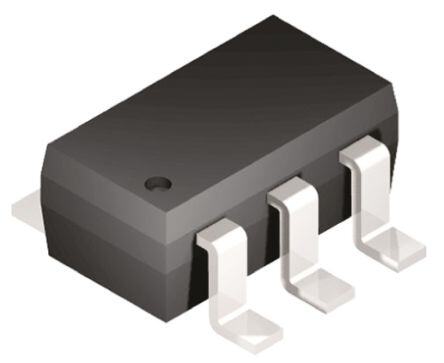
| 供应商器件封装 | SOT-23-6 |
| 其它名称 | 296-15568-6 |
| 包装 | Digi-Reel® |
| 单位重量 | 6.500 mg |
| 商标 | Texas Instruments |
| 安装类型 | 表面贴装 |
| 安装风格 | SMD/SMT |
| 封装 | Reel |
| 封装/外壳 | SOT-23-6 |
| 封装/箱体 | SOT-23-6 |
| 工作温度 | -40°C ~ 85°C |
| 工作温度范围 | - 40 C to + 85 C |
| 工作电压 | 1.65 V to 5.5 V |
| 工厂包装数量 | 3000 |
| 最大工作温度 | + 85 C |
| 最小工作温度 | - 40 C |
| 标准包装 | 1 |
| 独立电路 | 1 |
| 电压-电源 | 1.65 V ~ 5.5 V |
| 电压源 | 单电源 |
| 电流-输出高,低 | 32mA,32mA |
| 电源电压-最大 | 5.5 V |
| 电源电压-最小 | 1.65 V |
| 电路 | 1 x 1:2 |
| 类型 | 多路分解器 |
| 系列 | SN74LVC1G18 |
| 输入/输出线数量 | 1 / 2 |
| 输入线路数量 | 1 |
| 输出线路数量 | 2 |
| 逻辑系列 | LVC |


- 商务部:美国ITC正式对集成电路等产品启动337调查
- 曝三星4nm工艺存在良率问题 高通将骁龙8 Gen1或转产台积电
- 太阳诱电将投资9.5亿元在常州建新厂生产MLCC 预计2023年完工
- 英特尔发布欧洲新工厂建设计划 深化IDM 2.0 战略
- 台积电先进制程称霸业界 有大客户加持明年业绩稳了
- 达到5530亿美元!SIA预计今年全球半导体销售额将创下新高
- 英特尔拟将自动驾驶子公司Mobileye上市 估值或超500亿美元
- 三星加码芯片和SET,合并消费电子和移动部门,撤换高东真等 CEO
- 三星电子宣布重大人事变动 还合并消费电子和移动部门
- 海关总署:前11个月进口集成电路产品价值2.52万亿元 增长14.8%


PDF Datasheet 数据手册内容提取
Product Order Technical Tools & Support & Folder Now Documents Software Community SN74LVC1G18 SCES406L–JULY2002–REVISEDAUGUST2019 SN74LVC1G18 1-of-2 Noninverting Demultiplexer With 3-State Deselected Output 1 Features 3 Description • Operatingtemperaturefrom –40°Cto+125°C This non-inverting demultiplexer is designed for 1.65- 1 Vto5.5-VV operation. • Supports5-VV operation CC CC The SN74LVC1G18 device is a 1-of-2 non-inverting • Inputsacceptvoltagesto5.5V demultiplexer with a 3-state output. This device • SupportsdowntranslationtoV CC buffers the data on input A and passes it to either • Maxt of3.4nsat3.3V output Y0 or Y1, depending on whether the state of pd • Lowpowerconsumption,10-µAmaxI theselect(S)inputisloworhigh,respectively. CC • ±24-mAOutputdriveat3.3V NanoFree™ package technology is a major • TypicalV (outputgroundbounce) breakthrough in IC packaging concepts, using the die OLP asthepackage. <0.8VatV =3.3V,T =25°C CC A • TypicalV (outputV undershoot) This device is fully specified for partial-power-down OHV OH >2VatVCC=3.3V,TA=25°C applications using Ioff. The Ioff circuitry disables the outputs, preventing damaging current backflow • I Supportsliveinsertion,partial-power-down off throughthedevicewhenitispowereddown. mode,andback-driveprotection • Latch-upperformanceexceeds100mA DeviceInformation(1) PerJESD78,ClassII PARTNUMBER PACKAGE BODYSIZE(NOM) • ESDprotectionexceedsJESD22 SN74LVC1G18DBVR SOT-23(6) 2.90mm×2.80mm – 2000-VHuman-bodymodel(A114-A) SN74LVC1G18DCKR SC70(6) 2.00mm×1.10mm – 200-Vmachinemodel(A115-A) SN74LVC1G18DRYR SON(6) 1.45mm×1.00mm – 1000-VCharged-devicemodel(C101) SN74LVC1G18DSFR SON(6) 1.00mm×1.00mm SN74LVC1G18YZPR DSBGA(6) 1.39mm×0.89mm 2 Applications (1) For all available packages, see the orderable addendum at • Datacenterswitch theendofthedatasheet. • Basebandunit(BBU) • Wi-Fiaccesspoint • NotebookPC • Activeantennasystem(AAS) • Appliances • Industrialmonitor • Coffeemachine • Wiredspeaker • Vacuumrobot • Professionalaudiointerface SimplifiedSchematic 6 Y0 1 S 3 4 A Y1 1 An IMPORTANT NOTICE at the end of this data sheet addresses availability, warranty, changes, use in safety-critical applications, intellectualpropertymattersandotherimportantdisclaimers.PRODUCTIONDATA.
SN74LVC1G18 SCES406L–JULY2002–REVISEDAUGUST2019 www.ti.com Table of Contents 1 Features.................................................................. 1 8.2 FunctionalBlockDiagram.......................................11 2 Applications........................................................... 1 8.3 FeatureDescription.................................................11 3 Description............................................................. 1 8.4 DeviceFunctionalModes........................................12 4 RevisionHistory..................................................... 2 9 ApplicationandImplementation........................ 13 9.1 ApplicationInformation............................................13 5 PinConfigurationandFunctions......................... 3 9.2 TypicalApplication..................................................13 6 Specifications......................................................... 5 10 PowerSupplyRecommendations..................... 16 6.1 AbsoluteMaximumRatings .....................................5 11 Layout................................................................... 16 6.2 ESDRatings..............................................................5 6.3 RecommendedOperatingConditions......................6 11.1 LayoutGuidelines.................................................16 6.4 ThermalInformation..................................................6 11.2 LayoutExample....................................................16 6.5 ElectricalCharacteristics...........................................7 12 DeviceandDocumentationSupport................. 17 6.6 SwitchingCharacteristics,–40to85°C....................7 12.1 DocumentationSupport .......................................17 6.7 SwitchingCharacteristics,–40to125°C...................7 12.2 ReceivingNotificationofDocumentationUpdates17 6.8 OperatingCharacteristics..........................................8 12.3 CommunityResources..........................................17 6.9 TypicalCharacteristics..............................................8 12.4 Trademarks...........................................................17 7 ParameterMeasurementInformation..................9 12.5 ElectrostaticDischargeCaution............................17 12.6 Glossary................................................................17 8 DetailedDescription............................................ 11 13 Mechanical,Packaging,andOrderable 8.1 Overview.................................................................11 Information........................................................... 17 4 Revision History NOTE:Pagenumbersforpreviousrevisionsmaydifferfrompagenumbersinthecurrentversion. ChangesfromRevisionK(July2012)toRevisionL Page • UpdateddocumenttonewTIdatasheetformat.................................................................................................................... 1 • DeletedOrderingInformationtable........................................................................................................................................ 1 • UpdatedI inFeatures.......................................................................................................................................................... 1 off • AddedApplications................................................................................................................................................................. 1 • AddedDeviceInformationtable............................................................................................................................................. 1 • AddedOperatingjunctiontemperature................................................................................................................................... 5 • AddedHandlingRatingstable................................................................................................................................................ 5 • AddedThermalInformationtable........................................................................................................................................... 6 2 SubmitDocumentationFeedback Copyright©2002–2019,TexasInstrumentsIncorporated ProductFolderLinks:SN74LVC1G18
SN74LVC1G18 www.ti.com SCES406L–JULY2002–REVISEDAUGUST2019 5 Pin Configuration and Functions DRYandDSFPackage YZPPackage 6-PinSON 6-PinDSBGA TransparentTopView BottomView S 1 6 Y 0 GND V 2 5 CC A Y C1 C2 1 A 3 4 Y GND V 1 B1 B2 CC S Y A1 A2 0 DBVandDCKPackage 6-PinSOT-23andSC70 TopView S Y 1 6 0 GND V 2 5 CC A Y 3 4 1 Nottoscale.Seethemechanicaldrawingsattheendofthedatasheetforpackagedimensions. PinFunctions PIN DBV,DCK, I/O DESCRIPTION NAME YZP DRY,DSF S 1 A1 Input Activeoutputselection(LOW=Y0,HIGH=Y1) GND 2 B1 — Ground A 3 C1 Input InputA Y1 4 C2 Output OutputY1 VCC 5 B2 — Positivesupply Y0 6 A2 Output OutputY0 Copyright©2002–2019,TexasInstrumentsIncorporated SubmitDocumentationFeedback 3 ProductFolderLinks:SN74LVC1G18
SN74LVC1G18 SCES406L–JULY2002–REVISEDAUGUST2019 www.ti.com LogicDiagram(PositiveLogic) 6 Y0 1 S 3 4 A Y1 4 SubmitDocumentationFeedback Copyright©2002–2019,TexasInstrumentsIncorporated ProductFolderLinks:SN74LVC1G18
SN74LVC1G18 www.ti.com SCES406L–JULY2002–REVISEDAUGUST2019 6 Specifications 6.1 Absolute Maximum Ratings overoperatingfree-airtemperaturerange(unlessotherwisenoted)(1) MIN MAX UNIT V Supplyvoltagerange –0.5 6.5 V CC V Inputvoltagerange(2) –0.5 6.5 V I V Voltagerangeappliedtoanyoutputinthehigh-impedanceorpower-offstate(3) –0.5 6.5 V O V Voltagerangeappliedtoanyoutputinthehighorlowstate(2)(1) –0.5 V +0.5 V O CC I Inputclampcurrent V <0 –50 mA IK I I Outputclampcurrent V <0 –50 mA OK O I Continuousoutputcurrent ±50 mA O ContinuouscurrentthroughV orGND ±100 mA CC T Operatingjunctiontemperature 150 °C J T Storagetemperature –65 150 °C stg (1) StressesbeyondthoselistedunderAbsoluteMaximumRatingsmaycausepermanentdamagetothedevice.Thesearestressratings only,andfunctionaloperationofthedeviceattheseoranyotherconditionsbeyondthoseindicatedunderRecommendedOperating Conditionsisnotimplied.Exposuretoabsolute-maximum-ratedconditionsforextendedperiodsmayaffectdevicereliability. (2) Theinputnegative-voltageandoutputvoltageratingsmaybeexceedediftheinputandoutputcurrentratingsareobserved. (3) ThevalueofV isprovidedintheRecommendedOperatingConditionstable. CC 6.2 ESD Ratings VALUE UNIT Electrostatic Humanbodymodel(HBM),perANSI/ESDA/JEDECJS-001 (1) 2000 V V (ESD) discharge Chargeddevicemodel(CDM),perJEDECspecificationJESD22-C101 (2) 1000 (1) JEDECdocumentJEP155statesthat500-VHBMallowssafemanufacturingwithastandardESDcontrolprocess. (2) JEDECdocumentJEP157statesthat250-VCDMallowssafemanufacturingwithastandardESDcontrolprocess. Copyright©2002–2019,TexasInstrumentsIncorporated SubmitDocumentationFeedback 5 ProductFolderLinks:SN74LVC1G18
SN74LVC1G18 SCES406L–JULY2002–REVISEDAUGUST2019 www.ti.com 6.3 Recommended Operating Conditions overoperatingfree-airtemperaturerange(unlessotherwisenoted)(1) MIN MAX UNIT Operating 1.65 5.5 V Supplyvoltage V CC Dataretentiononly 1.5 V =1.65Vto1.95V 0.65×V CC CC V =2.3Vto2.7V 1.7 CC V High-levelinputvoltage V IH V =3Vto3.6V 2 CC V =4.5Vto5.5V 0.7×V CC CC V =1.65Vto1.95V 0.35×V CC CC V =2.3Vto2.7V 0.7 CC V Low-levelinputvoltage V IL V =3Vto3.6V 0.8 CC V =4.5Vto5.5V 0.3×V CC CC V Inputvoltage 0 5.5 V I V Outputvoltage 0 V V O CC V =1.65V –4 CC V =2.3V –8 CC I High-leveloutputcurrent –16 mA OH V =3V CC –24 V =4.5V –32 CC V =1.65V 4 CC V =2.3V 8 CC I Low-leveloutputcurrent 16 mA OL V =3V CC 24 V =4.5V 32 CC V =1.8V±0.15V,2.5V±0.2V 20 CC Δt/Δv Inputtransitionriseorfallrate V =3.3V±0.3V 10 ns/V CC V =5V±0.5V 5 CC T Operatingfree-airtemperature –40 125 °C A (1) AllunusedinputsofthedevicemustbeheldatV orGNDtoensureproperdeviceoperation.RefertotheTIapplicationreport, CC ImplicationsofSloworFloatingCMOSInputs,literaturenumberSCBA004. 6.4 Thermal Information SN74LVC1G18 THERMALMETRIC(1) DBV DCK DRY DSF YZP UNIT 6PINS 6PINS 6PINS 6PINS 6PINS R Junction-to-ambientthermalresistance 236.1 278.7 306.7 300.3 123.8 °C/W θJA R Junction-to-case(top)thermalresistance 174.0 217.8 207.2 183.5 1.4 °C/W θJC(top) R Junction-to-boardthermalresistance 111.5 124.6 181.1 170.7 38.9 °C/W θJB ψ Junction-to-topcharacterizationparameter 93.5 105.2 49.9 24.2 0.5 °C/W JT ψ Junction-to-boardcharacterizationparameter 111.2 124.1 180.3 170.2 38.9 °C/W JB R Junction-to-case(bottom)thermalresistance N/A N/A N/A N/A N/A °C/W θJC(bot) (1) Formoreinformationabouttraditionalandnewthermalmetrics,seetheICPackageThermalMetricsapplicationreport,SPRA953. 6 SubmitDocumentationFeedback Copyright©2002–2019,TexasInstrumentsIncorporated ProductFolderLinks:SN74LVC1G18
SN74LVC1G18 www.ti.com SCES406L–JULY2002–REVISEDAUGUST2019 6.5 Electrical Characteristics overrecommendedoperatingfree-airtemperaturerange(unlessotherwisenoted) -40to85°C -40to125°C PARAMETE TESTCONDITIONS V MIN TYP(1) MAX MIN TYP(1) MAX UNIT R CC 1.65Vto V – V – I =–100µA CC CC OH 5.5V 0.1 0.1 I =–4mA 1.65V 1.2 1.2 OH VOH IOH=–8mA 2.3V 1.9 1.9 V I =–16mA 2.4 2.4 OH 3V I =–24mA 2.3 2.3 OH I =–32mA 4.5V 3.8 3.8 OH 1.65Vto I =100µA 0.1 0.1 OL 5.5V I =4mA 1.65V 0.45 0.45 OL VOL IOL=8mA 2.3V 0.3 0.3 V I =16mA 0.4 0.4 OL 3V I =24mA 0.55 0.55 OL I =32mA 4.5V 0.55 0.55 OL I V =5.5VorGND 0to5.5V ±5 ±5 µA I I I V orV =5.5V 0 ±10 ±10 µA off I O I V =0to5.5V 3.6V 10 10 µA OZ O 1.65Vto I V =5.5VorGND, I =0 10 10 µA CC I O 5.5V Oneinputat OtherinputsatV or 3Vto5.5 ΔI CC 500 500 µA CC V –0.6V, GND V CC C V =V orGND 3.3V 4 4 pF I I CC C V =V orGND 3.3V 6 6 pF o O CC (1) AlltypicalvaluesareatV =3.3V,T =25°C. CC A 6.6 Switching Characteristics, –40 to 85°C T =–40to85°C,C =30pFor50pF(unlessotherwisenoted)(seeParameterMeasurementInformation) A L V =1.8V V =2.5V V =3.3V V =5V CC CC CC CC PARA FROM TO CONDITION ±0.15V ±0.2V ±0.3V ±0.5V UNIT METER (INPUT) (OUTPUT) MIN MAX MIN MAX MIN MAX MIN MAX C =15pF 2.3 8.4 1.1 4.2 1.1 3.4 0.8 2.7 ns L t A Y pd C =30pFor50pF 3.5 9.3 1.7 5 1.5 4.2 0.7 3.2 ns L t S Y C =30pFor50pF 3.6 10.2 1.7 5.6 1.5 4.6 0.9 3.4 ns en L t S Y C =30pFor50pF 1.9 12.7 1 5.3 1.1 4.9 0.5 3.3 ns dis L 6.7 Switching Characteristics, –40 to 125°C overrecommendedoperatingfree-airtemperaturerange,C =30pFor50pF(unlessotherwisenoted)(seeParameter L MeasurementInformation) V =1.8V V =2.5V V =3.3V V =5V CC CC CC CC PARA FROM TO CONDITION ±0.15V ±0.2V ±0.3V ±0.5V UNIT METER (INPUT) (OUTPUT) MIN MAX MIN MAX MIN MAX MIN MAX t A Y C =30pFor50pF 3.5 9.8 1.7 5.5 1.5 4.7 0.7 3.7 ns pd L t S Y C =30pFor50pF 3.6 11.2 1.7 6.6 1.5 6.1 0.9 4.9 ns en L t S Y C =30pFor50pF 1.9 13.7 1 6.3 1.1 6.4 0.5 4.8 ns dis L Copyright©2002–2019,TexasInstrumentsIncorporated SubmitDocumentationFeedback 7 ProductFolderLinks:SN74LVC1G18
SN74LVC1G18 SCES406L–JULY2002–REVISEDAUGUST2019 www.ti.com 6.8 Operating Characteristics T =25°C A TEST VCC=1.8V VCC=2.5V VCC=3.3V VCC=5V PARAMETER UNIT CONDITIONS TYP TYP TYP TYP C Powerdissipationcapacitance f=10MHz 17 17 18 21 pF pd 6.9 Typical Characteristics T =25°C;Simulateddata A 0.5 5 0.45 4.5 V) V) 0.4 e ( 4 w output voltage ( 00..0023..2355 evel output voltag 23..2355 V, LoOL 00..001.155 VVVCCCCCC === 123...853 VVV V, High-lOH 01..155 VVVCCCCCC === 123...853 VVV 0 VCC = 5 V 0 VCC = 5 V 0 4 8 12 16 20 24 28 32 36 40 0 5 10 15 20 25 30 35 40 45 50 IOL, Low-level output current (mA) IOH, High-level output current (mA) Figure1.Typicallow-leveloutputvoltageatcommonsupply Figure2.Typicalhigh-leveloutputvoltageatcommon valuesandcurrents supplyvaluesandcurrents 8 SubmitDocumentationFeedback Copyright©2002–2019,TexasInstrumentsIncorporated ProductFolderLinks:SN74LVC1G18
SN74LVC1G18 www.ti.com SCES406L–JULY2002–REVISEDAUGUST2019 7 Parameter Measurement Information V LOAD R S1 Open From Output L TEST S1 Under Test GND t /t Open C PLH PHL (see NoteA)L RL tPLZ/tPZL VLOAD t /t GND PHZ PZH LOAD CIRCUIT INPUTS V V V C R V CC V t/t M LOAD L L D I r f 1.8 V±0.15 V V £2 ns V /2 2 ×V 15 pF 1 MW 0.15 V CC CC CC 2.5 V±0.2 V V £2 ns V /2 2 ×V 15 pF 1 MW 0.15 V CC CC CC 3.3 V±0.3 V 3 V £2.5 ns 1.5 V 6 V 15 pF 1 MW 0.3 V 5 V±0.5 V V £2.5 ns V /2 2 ×V 15 pF 1 MW 0.3 V CC CC CC V I Timing Input V M 0 V t W VI tsu th V Input V V I M M Data Input V V M M 0 V 0 V VOLTAGE WAVEFORMS VOLTAGE WAVEFORMS PULSE DURATION SETUPAND HOLD TIMES Input VM VM VI COounttpruotl VM VM VI 0 V 0 V t t t t PLH PHL PZL PLZ V Output V /2 Output VM VM OH WSav1e afot rVm 1 VM V + V LOAD VOL (see NoteL OBAD) OL D VOL t t PHL PLH t t PZH PHZ Output VM VM VOH WSa1v eaOfto uGrtmpNu D2t VM VOH–VD VOH VOL (see Note B) »0 V VOLTAGE WAVEFORMS VOLTAGE WAVEFORMS PROPAGATION DELAYTIMES ENABLEAND DISABLE TIMES INVERTINGAND NONINVERTING OUTPUTS LOW-AND HIGH-LEVELENABLING NOTES: A. C includes probe and jig capacitance. L B. Waveform 1 is for an output with internal conditions such that the output is low, except when disabled by the output control. Waveform 2 is for an output with internal conditions such that the output is high, except when disabled by the output control. C. All input pulses are supplied by generators having the following characteristics: PRR£10 MHz, Z = 50W. O D. The outputs are measured one at a time, with one transition per measurement. E. t and t are the same as t . PLZ PHZ dis F. t and t are the same as t . PZL PZH en G.t and t are the same as t . PLH PHL pd H. All parameters and waveforms are not applicable to all devices. Figure3. LoadCircuitandVoltageWaveforms Copyright©2002–2019,TexasInstrumentsIncorporated SubmitDocumentationFeedback 9 ProductFolderLinks:SN74LVC1G18
SN74LVC1G18 SCES406L–JULY2002–REVISEDAUGUST2019 www.ti.com Parameter Measurement Information (continued) V LOAD R S1 Open From Output L TEST S1 Under Test GND t /t Open C PLH PHL (see NoteA)L RL tPLZ/tPZL VLOAD t /t GND PHZ PZH LOAD CIRCUIT INPUTS V V V C R V CC V t/t M LOAD L L D I r f 1.8 V±0.15 V V £2 ns V /2 2 ×V 30 pF 1 kW 0.15 V CC CC CC 2.5 V±0.2 V V £2 ns V /2 2 ×V 30 pF 500W 0.15 V CC CC CC 3.3 V±0.3 V 3 V £2.5 ns 1.5 V 6 V 50 pF 500W 0.3 V 5 V±0.5 V V £2.5 ns V /2 2 ×V 50 pF 500W 0.3 V CC CC CC V I Timing Input V M 0 V t W VI tsu th V Input V V I M M Data Input V V M M 0 V 0 V VOLTAGE WAVEFORMS VOLTAGE WAVEFORMS PULSE DURATION SETUPAND HOLD TIMES Input VM VM VI COounttpruotl VM VM VI 0 V 0 V t t t t PLH PHL PZL PLZ V Output V /2 Output VM VM OH WSav1e afot rVm 1 VM V + V LOAD VOL (see NoteL OBAD) OL D VOL t t PHL PLH t t PZH PHZ Output VM VM VOH WSa1v eaOfto uGrtmpNu D2t VM VOH–VD VOH VOL (see Note B) »0 V VOLTAGE WAVEFORMS VOLTAGE WAVEFORMS PROPAGATION DELAYTIMES ENABLEAND DISABLE TIMES INVERTINGAND NONINVERTING OUTPUTS LOW-AND HIGH-LEVELENABLING NOTES: A. C includes probe and jig capacitance. L B. Waveform 1 is for an output with internal conditions such that the output is low, except when disabled by the output control. Waveform 2 is for an output with internal conditions such that the output is high, except when disabled by the output control. C. All input pulses are supplied by generators having the following characteristics: PRR£10 MHz, Z = 50W. O D. The outputs are measured one at a time, with one transition per measurement. E. t and t are the same as t . PLZ PHZ dis F. t and t are the same as t . PZL PZH en G.t and t are the same as t . PLH PHL pd H. All parameters and waveforms are not applicable to all devices. Figure4. LoadCircuitandVoltageWaveforms 10 SubmitDocumentationFeedback Copyright©2002–2019,TexasInstrumentsIncorporated ProductFolderLinks:SN74LVC1G18
SN74LVC1G18 www.ti.com SCES406L–JULY2002–REVISEDAUGUST2019 8 Detailed Description 8.1 Overview This device contains one independent 1-of-2 noninverting demultiplexer with high-impedance outputs when disabled. 8.2 Functional Block Diagram 6 Y0 1 S 3 4 A Y1 8.3 Feature Description 8.3.1 BalancedCMOS3-StateOutputs A balanced output allows the device to sink and source similar currents. The drive capability of this device may create fast edges into light loads so routing and load conditions should be considered to prevent ringing. Additionally, the outputs of this device are capable of driving larger currents than the device can sustain without being damaged. It is important for the output power of the device to be limited to avoid damage due to over- current.TheelectricalandthermallimitsdefinedintheAbsoluteMaximumRatings mustbefollowedatalltimes. 3-State outputs can be placed into a high-impedance state. In this state, the output will neither source nor sink current, and leakage current is defined by the I specification in the Electrical Characteristics. A pull-up or pull- OZ down resistor can be used to ensure that the output remains HIGH or LOW, respectively, during the high- impedancestate. 8.3.2 PartialPowerDown(I ) off The inputs and outputs for this device enter a high-impedance state when the device is powered down, inhibiting current backflow into the device. The maximum leakage into or out of any input or output pin on the device is specifiedbyI intheElectricalCharacteristics. off 8.3.3 StandardCMOSInputs Standard CMOS inputs are high impedance and are typically modeled as a resistor in parallel with the input capacitance given in the Electrical Characteristics. The worst case resistance is calculated with the maximum input voltage, given in the Absolute Maximum Ratings , and the maximum input leakage current, given in the ElectricalCharacteristics,usingohm'slaw(R=V ÷ I). Signals applied to the inputs need to have fast edge rates, as defined by Δt/Δv in the Recommended Operating Conditions to avoid excessive current consumption and oscillations. If a slow or noisy input signal is required, a devicewithaSchmitt-triggerinputshouldbeusedtoconditiontheinputsignalpriortothestandardCMOSinput. 8.3.4 Over-voltageTolerantInputs Input signals to this device can be driven above the supply voltage so long as they remain below the maximum inputvoltagevaluespecifiedintheRecommendedOperatingConditions. 8.3.5 ClampDiodeStructure TheinputsandoutputstothisdevicehavenegativeclampingdiodesonlyasdepictedinFigure5. Copyright©2002–2019,TexasInstrumentsIncorporated SubmitDocumentationFeedback 11 ProductFolderLinks:SN74LVC1G18
SN74LVC1G18 SCES406L–JULY2002–REVISEDAUGUST2019 www.ti.com Feature Description (continued) CAUTION Voltages beyond the values specified in the Absolute Maximum Ratings table can cause damage to the device. The input negative-voltage and output voltage ratings maybeexceedediftheinputandoutputclamp-currentratingsareobserved. Device VCC Input Logic Output -IIK -IOK GND Figure5. ElectricalPlacementofClampingDiodesforEachInputandOutput 8.4 Device Functional Modes Table1.FunctionTable INPUTS OUTPUTS S A Y0 Y1 L L L Z L H H Z H L Z L H H Z H 12 SubmitDocumentationFeedback Copyright©2002–2019,TexasInstrumentsIncorporated ProductFolderLinks:SN74LVC1G18
SN74LVC1G18 www.ti.com SCES406L–JULY2002–REVISEDAUGUST2019 9 Application and Implementation NOTE Information in the following applications sections is not part of the TI component specification, and TI does not warrant its accuracy or completeness. TI’s customers are responsible for determining suitability of components for their purposes. Customers should validateandtesttheirdesignimplementationtoconfirmsystemfunctionality. 9.1 Application Information The SN74LVC1G18 can be used to select between controlling two analog switches. In this use case, pull-down resistors are connected to both outputs of the SN74LVC1G18 to ensure that a valid state is available for the inputs to the switches at all times. This defaults the switches into the "off" state to prevent unwanted data transmission. 9.2 Typical Application SN74LVC1G18 VCC 0.1 (cid:29)F Y 0 10 k(cid:13)(cid:3) S System Analog Controller A Y 1 Switches 10 k(cid:13)(cid:3) Figure6. Typicalapplicationblockdiagram 9.2.1 DesignRequirements • Eachanalogswitchmustbecontrolledbythesystemcontroller,butonlywhentheotherswitchisdisabled. • WhentheinputSislow,theY outputisselectedandtheY outputisinthehighimpedancestate 0 1 • WhentheinputSishigh,theY outputisselectedandtheY outputisinthehighimpedancestate 1 0 • WhentheinputAishigh,theselectedanalogswitchmustbeclosed • WhentheinputAislow,theselectedanalogswitchmustbeopen 9.2.1.1 PowerConsiderations Ensure the desired supply voltage is within the range specified in the Recommended Operating Conditions . The supplyvoltagesetsthedevice'selectricalcharacteristicsasdescribedintheElectricalCharacteristics. The supply must be capable of sourcing current equal to the total current to be sourced by all outputs of the SN74LVC1G18 plus the maximum supply current, I , listed in the Electrical Characteristics. The logic device CC canonlysourceorsinkasmuchcurrentas it is provided at the supply and ground pins, respectively. Be sure not toexceedthemaximumtotalcurrentthroughGNDorV listedintheAbsoluteMaximumRatings. CC The SN74LVC1G18 can drive a load with a total capacitance less than or equal to 50 pF connected to a high- impedance CMOS input while still meeting all of the datasheet specifications. Larger capacitive loads can be applied,howeveritisnotrecommendedtoexceed70pF. Copyright©2002–2019,TexasInstrumentsIncorporated SubmitDocumentationFeedback 13 ProductFolderLinks:SN74LVC1G18
SN74LVC1G18 SCES406L–JULY2002–REVISEDAUGUST2019 www.ti.com Typical Application (continued) Total power consumption can be calculated using the information provided in CMOS Power Consumption and C Calculation. pd Thermal increase can be calculated using the information provided in Thermal Characteristics of Standard Linear andLogic(SLL)PackagesandDevices. CAUTION The maximum junction temperature, T (max) listed in the Absolute Maximum Ratings , J is an additional limitation to prevent damage to the device. Do not violate any values listed in the Absolute Maximum Ratings . These limits are provided to prevent damage tothedevice. 9.2.1.2 InputConsiderations Unused inputs must be terminated to either V or ground. These can be directly terminated if the input is CC completely unused, or they can be connected with a pull-up or pull-down resistor if the input is to be used sometimes,butnotalways.A pull-up resistor is used for a default state of HIGH, and a pull-down resistor is used for a default state of LOW. The resistor size is limited by drive current of the controller, leakage current into the SN74LVC1G18, as specified in the Electrical Characteristics, and the desired input transition rate. A 10-kΩ resistorvalueisoftenusedduetothesefactors. The SN74LVC1G18 has standard CMOS inputs, so input signal edge rates cannot be slow. Slow input edge rates can cause oscillations and damaging shoot-through current. The recommended rates are defined in the RecommendedOperatingConditions. RefertotheFeatureDescriptionforadditionalinformationregardingtheinputsforthisdevice. 9.2.1.3 OutputConsiderations The positive supply voltage is used to produce the output HIGH voltage. Drawing current from the output will decrease the output voltage as specified by the V specification in the Electrical Characteristics. Similarly, the OH ground voltage is used to produce the output LOW voltage. Sinking current into the output will increase the output voltage as specified by the V specification in the Electrical Characteristics. The plots in the Typical OL Characteristicsprovidearelationshipbetweenoutputvoltageandcurrentforthisdevice. Unusedoutputscanbeleftfloating. RefertoFeatureDescriptionforadditionalinformationregardingtheoutputsforthisdevice. 9.2.2 DetailedDesignProcedure 1. Add a decoupling capacitor from V to GND. The capacitor needs to be placed physically close to the CC deviceandelectricallyclosetoboththeV andGNDpins.AnexamplelayoutisshownintheLayout. CC 2. Ensure the capacitive load at the output is ≤ 70 pF. This is not a hard limit, however it will ensure optimal performance. This can be accomplished by providing short, appropriately sized traces from the SN74LVC1G18tothereceivingdevice. 3. Ensure the resistive load at the output is larger than (V / 25 mA) Ω. This will ensure that the maximum CC output current from the Absolute Maximum Ratings is not violated. Most CMOS inputs have a resistive load measuredinmegohms;muchlargerthantheminimumcalculatedabove. 4. Thermal issues are rarely a concern for logic gates, however the power consumption and thermal increase can be calculated using the steps provided in the application report, CMOS Power Consumption and Cpd Calculation 14 SubmitDocumentationFeedback Copyright©2002–2019,TexasInstrumentsIncorporated ProductFolderLinks:SN74LVC1G18
SN74LVC1G18 www.ti.com SCES406L–JULY2002–REVISEDAUGUST2019 Typical Application (continued) 9.2.3 ApplicationCurves Figure7. Simulatedapplicationtransientresponse Copyright©2002–2019,TexasInstrumentsIncorporated SubmitDocumentationFeedback 15 ProductFolderLinks:SN74LVC1G18
SN74LVC1G18 SCES406L–JULY2002–REVISEDAUGUST2019 www.ti.com 10 Power Supply Recommendations The power supply can be any voltage between the minimum and maximum supply voltage rating located in the Recommended Operating Conditions . Each V terminal should have a good bypass capacitor to prevent power CC disturbance. A 0.1-μF capacitor is recommended for this device. It is acceptable to parallel multiple bypass caps to reject different frequencies of noise. The 0.1-μF and 1-μF capacitors are commonly used in parallel. The bypass capacitor should be installed as close to the power terminal as possible for best results, as shown in Figure8. 11 Layout 11.1 Layout Guidelines When using multiple-input and multiple-channel logic devices inputs must not ever be left floating. In many cases, functions or parts of functions of digital logic devices are unused; for example, when only two inputs of a triple-input AND gate are used or only 3 of the 4 buffer gates are used. Such unused input pins must not be left unconnected because the undefined voltages at the outside connections result in undefined operational states. Allunusedinputs of digital logic devices must be connected to a logic high or logic low voltage, as defined by the input voltage specifications, to prevent them from floating. The logic level that must be applied to any particular unused input depends on the function of the device. Generally, the inputs are tied to GND or V , whichever CC makesmoresenseforthelogicfunctionorismoreconvenient. 11.2 Layout Example V CC Avoid 90° corners for Unused output signal lines left floating S A1 A2 D N G 0.1 (cid:29)F GND B1 B2 V CC A C1 C2 Y 1 Unused input tied Bypass capacitor placed to GND close to the device Figure8. ExamplelayoutfortheSN74LVC1G18 16 SubmitDocumentationFeedback Copyright©2002–2019,TexasInstrumentsIncorporated ProductFolderLinks:SN74LVC1G18
SN74LVC1G18 www.ti.com SCES406L–JULY2002–REVISEDAUGUST2019 12 Device and Documentation Support 12.1 Documentation Support 12.1.1 RelatedDocumentation Forrelateddocumentationseethefollowing: • ImplicationsofSloworFloatingCMOSInputs • CMOSPowerConsumptionandC Calculation pd • UnderstandingandInterpretingStandard-LogicDataSheets 12.2 Receiving Notification of Documentation Updates To receive notification of documentation updates, navigate to the device product folder on ti.com. In the upper right corner, click on Alert me to register and receive a weekly digest of any product information that has changed.Forchangedetails,reviewtherevisionhistoryincludedinanyreviseddocument. 12.3 Community Resources The following links connect to TI community resources. Linked contents are provided "AS IS" by the respective contributors. They do not constitute TI specifications and do not necessarily reflect TI's views; see TI's Terms of Use. TIE2E™OnlineCommunity TI'sEngineer-to-Engineer(E2E)Community.Createdtofostercollaboration amongengineers.Ate2e.ti.com,youcanaskquestions,shareknowledge,exploreideasandhelp solveproblemswithfellowengineers. DesignSupport TI'sDesignSupport QuicklyfindhelpfulE2Eforumsalongwithdesignsupporttoolsand contactinformationfortechnicalsupport. 12.4 Trademarks NanoFree,E2EaretrademarksofTexasInstruments. 12.5 Electrostatic Discharge Caution This integrated circuit can be damaged by ESD. Texas Instruments recommends that all integrated circuits be handled with appropriateprecautions.Failuretoobserveproperhandlingandinstallationprocedurescancausedamage. ESDdamagecanrangefromsubtleperformancedegradationtocompletedevicefailure.Precisionintegratedcircuitsmaybemore susceptibletodamagebecauseverysmallparametricchangescouldcausethedevicenottomeetitspublishedspecifications. 12.6 Glossary SLYZ022—TIGlossary. Thisglossarylistsandexplainsterms,acronyms,anddefinitions. 13 Mechanical, Packaging, and Orderable Information The following pages include mechanical, packaging, and orderable information. This information is the most current data available for the designated devices. This data is subject to change without notice and revision of thisdocument.Forbrowser-basedversionsofthisdatasheet,refertotheleft-handnavigation. Copyright©2002–2019,TexasInstrumentsIncorporated SubmitDocumentationFeedback 17 ProductFolderLinks:SN74LVC1G18
PACKAGE OPTION ADDENDUM www.ti.com 6-Feb-2020 PACKAGING INFORMATION Orderable Device Status Package Type Package Pins Package Eco Plan Lead/Ball Finish MSL Peak Temp Op Temp (°C) Device Marking Samples (1) Drawing Qty (2) (6) (3) (4/5) SN74LVC1G18DBVR ACTIVE SOT-23 DBV 6 3000 Green (RoHS NIPDAU Level-1-260C-UNLIM -40 to 85 (C185, C18R) & no Sb/Br) SN74LVC1G18DBVRG4 ACTIVE SOT-23 DBV 6 3000 Green (RoHS NIPDAU Level-1-260C-UNLIM -40 to 85 (C185, C18R) & no Sb/Br) SN74LVC1G18DCKR ACTIVE SC70 DCK 6 3000 Green (RoHS NIPDAU | SN Level-1-260C-UNLIM -40 to 85 (CJ5, CJF, CJJ, CJ & no Sb/Br) K, CJR) SN74LVC1G18DCKRE4 ACTIVE SC70 DCK 6 3000 Green (RoHS NIPDAU Level-1-260C-UNLIM -40 to 85 CJ5 & no Sb/Br) SN74LVC1G18DCKRG4 ACTIVE SC70 DCK 6 3000 Green (RoHS NIPDAU Level-1-260C-UNLIM -40 to 85 CJ5 & no Sb/Br) SN74LVC1G18DRYR ACTIVE SON DRY 6 5000 Green (RoHS NIPDAU Level-1-260C-UNLIM -40 to 85 CJ & no Sb/Br) SN74LVC1G18DSFR ACTIVE SON DSF 6 5000 Green (RoHS NIPDAU Level-1-260C-UNLIM -40 to 85 CJ & no Sb/Br) SN74LVC1G18YZPR ACTIVE DSBGA YZP 6 3000 Green (RoHS SNAGCU Level-1-260C-UNLIM -40 to 85 CJN & no Sb/Br) (1) The marketing status values are defined as follows: ACTIVE: Product device recommended for new designs. LIFEBUY: TI has announced that the device will be discontinued, and a lifetime-buy period is in effect. NRND: Not recommended for new designs. Device is in production to support existing customers, but TI does not recommend using this part in a new design. PREVIEW: Device has been announced but is not in production. Samples may or may not be available. OBSOLETE: TI has discontinued the production of the device. (2) RoHS: TI defines "RoHS" to mean semiconductor products that are compliant with the current EU RoHS requirements for all 10 RoHS substances, including the requirement that RoHS substance do not exceed 0.1% by weight in homogeneous materials. Where designed to be soldered at high temperatures, "RoHS" products are suitable for use in specified lead-free processes. TI may reference these types of products as "Pb-Free". RoHS Exempt: TI defines "RoHS Exempt" to mean products that contain lead but are compliant with EU RoHS pursuant to a specific EU RoHS exemption. Green: TI defines "Green" to mean the content of Chlorine (Cl) and Bromine (Br) based flame retardants meet JS709B low halogen requirements of <=1000ppm threshold. Antimony trioxide based flame retardants must also meet the <=1000ppm threshold requirement. (3) MSL, Peak Temp. - The Moisture Sensitivity Level rating according to the JEDEC industry standard classifications, and peak solder temperature. (4) There may be additional marking, which relates to the logo, the lot trace code information, or the environmental category on the device. Addendum-Page 1
PACKAGE OPTION ADDENDUM www.ti.com 6-Feb-2020 (5) Multiple Device Markings will be inside parentheses. Only one Device Marking contained in parentheses and separated by a "~" will appear on a device. If a line is indented then it is a continuation of the previous line and the two combined represent the entire Device Marking for that device. (6) Lead/Ball Finish - Orderable Devices may have multiple material finish options. Finish options are separated by a vertical ruled line. Lead/Ball Finish values may wrap to two lines if the finish value exceeds the maximum column width. Important Information and Disclaimer:The information provided on this page represents TI's knowledge and belief as of the date that it is provided. TI bases its knowledge and belief on information provided by third parties, and makes no representation or warranty as to the accuracy of such information. Efforts are underway to better integrate information from third parties. TI has taken and continues to take reasonable steps to provide representative and accurate information but may not have conducted destructive testing or chemical analysis on incoming materials and chemicals. TI and TI suppliers consider certain information to be proprietary, and thus CAS numbers and other limited information may not be available for release. In no event shall TI's liability arising out of such information exceed the total purchase price of the TI part(s) at issue in this document sold by TI to Customer on an annual basis. Addendum-Page 2
PACKAGE MATERIALS INFORMATION www.ti.com 24-Apr-2020 TAPE AND REEL INFORMATION *Alldimensionsarenominal Device Package Package Pins SPQ Reel Reel A0 B0 K0 P1 W Pin1 Type Drawing Diameter Width (mm) (mm) (mm) (mm) (mm) Quadrant (mm) W1(mm) SN74LVC1G18DBVR SOT-23 DBV 6 3000 180.0 8.4 3.23 3.17 1.37 4.0 8.0 Q3 SN74LVC1G18DBVR SOT-23 DBV 6 3000 178.0 9.2 3.3 3.23 1.55 4.0 8.0 Q3 SN74LVC1G18DCKR SC70 DCK 6 3000 178.0 9.2 2.4 2.4 1.22 4.0 8.0 Q3 SN74LVC1G18DCKR SC70 DCK 6 3000 178.0 9.0 2.4 2.5 1.2 4.0 8.0 Q3 SN74LVC1G18DCKR SC70 DCK 6 3000 180.0 8.4 2.41 2.41 1.2 4.0 8.0 Q3 SN74LVC1G18DCKR SC70 DCK 6 3000 178.0 9.0 2.4 2.5 1.2 4.0 8.0 Q3 SN74LVC1G18DCKRG4 SC70 DCK 6 3000 178.0 9.2 2.4 2.4 1.22 4.0 8.0 Q3 SN74LVC1G18DRYR SON DRY 6 5000 180.0 9.5 1.15 1.6 0.75 4.0 8.0 Q1 SN74LVC1G18DSFR SON DSF 6 5000 180.0 9.5 1.16 1.16 0.5 4.0 8.0 Q2 SN74LVC1G18YZPR DSBGA YZP 6 3000 178.0 9.2 1.02 1.52 0.63 4.0 8.0 Q1 PackMaterials-Page1
PACKAGE MATERIALS INFORMATION www.ti.com 24-Apr-2020 *Alldimensionsarenominal Device PackageType PackageDrawing Pins SPQ Length(mm) Width(mm) Height(mm) SN74LVC1G18DBVR SOT-23 DBV 6 3000 202.0 201.0 28.0 SN74LVC1G18DBVR SOT-23 DBV 6 3000 180.0 180.0 18.0 SN74LVC1G18DCKR SC70 DCK 6 3000 180.0 180.0 18.0 SN74LVC1G18DCKR SC70 DCK 6 3000 180.0 180.0 18.0 SN74LVC1G18DCKR SC70 DCK 6 3000 202.0 201.0 28.0 SN74LVC1G18DCKR SC70 DCK 6 3000 180.0 180.0 18.0 SN74LVC1G18DCKRG4 SC70 DCK 6 3000 180.0 180.0 18.0 SN74LVC1G18DRYR SON DRY 6 5000 184.0 184.0 19.0 SN74LVC1G18DSFR SON DSF 6 5000 184.0 184.0 19.0 SN74LVC1G18YZPR DSBGA YZP 6 3000 220.0 220.0 35.0 PackMaterials-Page2
GENERIC PACKAGE VIEW DRY 6 USON - 0.6 mm max height PLASTIC SMALL OUTLINE - NO LEAD Images above are just a representation of the package family, actual package may vary. Refer to the product data sheet for package details. 4207181/G
PACKAGE OUTLINE DRY0006A USON - 0.6 mm max height SCALE 8.500 PLASTIC SMALL OUTLINE - NO LEAD B 1.05 A 0.95 PIN 1 INDEX AREA 1.5 1.4 0.6 MAX C SEATING PLANE 0.05 0.00 0.08 C 3X 0.6 SYMM (0.127) TYP (0.05) TYP 3 4 4X 0.5 SYMM 2X 1 6 1 0.25 6X 0.15 0.4 0.3 0.1 C A B 0.05 C PIN 1 ID (OPTIONAL) 0.35 5X 0.25 4222894/A 01/2018 NOTES: 1. All linear dimensions are in millimeters. Any dimensions in parenthesis are for reference only. Dimensioning and tolerancing per ASME Y14.5M. 2. This drawing is subject to change without notice. www.ti.com
EXAMPLE BOARD LAYOUT DRY0006A USON - 0.6 mm max height PLASTIC SMALL OUTLINE - NO LEAD SYMM (0.35) 5X (0.3) 1 6 6X (0.2) SYMM 4X (0.5) 4 3 (R0.05) TYP (0.6) LAND PATTERN EXAMPLE 1:1 RATIO WITH PKG SOLDER PADS EXPOSED METAL SHOWN SCALE:40X 0.05 MAX 0.05 MIN ALL AROUND ALL AROUND EXPOSED EXPOSED METAL METAL SOLDER MASK METAL METAL UNDER SOLDER MASK OPENING SOLDER MASK OPENING NON SOLDER MASK DEFINED SOLDER MASK DEFINED (PREFERRED) SOLDER MASK DETAILS 4222894/A 01/2018 NOTES: (continued) 3. For more information, see QFN/SON PCB application report in literature No. SLUA271 (www.ti.com/lit/slua271). www.ti.com
EXAMPLE STENCIL DESIGN DRY0006A USON - 0.6 mm max height PLASTIC SMALL OUTLINE - NO LEAD SYMM (0.35) 5X (0.3) 1 6 6X (0.2) SYMM 4X (0.5) 4 3 (R0.05) TYP (0.6) SOLDER PASTE EXAMPLE BASED ON 0.075 - 0.1 mm THICK STENCIL SCALE:40X 4222894/A 01/2018 NOTES: (continued) 4. Laser cutting apertures with trapezoidal walls and rounded corners may offer better paste release. IPC-7525 may have alternate design recommendations. www.ti.com
PACKAGE OUTLINE DBV0006A SOT-23 - 1.45 mm max height SCALE 4.000 SMALL OUTLINE TRANSISTOR C 3.0 2.6 0.1 C 1.75 1.45 B A 1.45 MAX PIN 1 INDEX AREA 1 6 2X 0.95 3.05 2.75 1.9 5 2 4 3 0.50 6X 0.25 0.15 0.2 C A B (1.1) TYP 0.00 0.25 GAGE PLANE 0.22 TYP 0.08 8 TYP 0.6 0 0.3 TYP SEATING PLANE 4214840/B 03/2018 NOTES: 1. All linear dimensions are in millimeters. Any dimensions in parenthesis are for reference only. Dimensioning and tolerancing per ASME Y14.5M. 2. This drawing is subject to change without notice. 3. Body dimensions do not include mold flash or protrusion. Mold flash and protrusion shall not exceed 0.15 per side. 4. Leads 1,2,3 may be wider than leads 4,5,6 for package orientation. 5. Refernce JEDEC MO-178. www.ti.com
EXAMPLE BOARD LAYOUT DBV0006A SOT-23 - 1.45 mm max height SMALL OUTLINE TRANSISTOR PKG 6X (1.1) 1 6X (0.6) 6 SYMM 2 5 2X (0.95) 3 4 (R0.05) TYP (2.6) LAND PATTERN EXAMPLE EXPOSED METAL SHOWN SCALE:15X SOLDER MASK SOLDER MASK METAL UNDER METAL OPENING OPENING SOLDER MASK EXPOSED METAL EXPOSED METAL 0.07 MAX 0.07 MIN ARROUND ARROUND NON SOLDER MASK SOLDER MASK DEFINED DEFINED (PREFERRED) SOLDER MASK DETAILS 4214840/B 03/2018 NOTES: (continued) 6. Publication IPC-7351 may have alternate designs. 7. Solder mask tolerances between and around signal pads can vary based on board fabrication site. www.ti.com
EXAMPLE STENCIL DESIGN DBV0006A SOT-23 - 1.45 mm max height SMALL OUTLINE TRANSISTOR PKG 6X (1.1) 1 6X (0.6) 6 SYMM 2 5 2X(0.95) 3 4 (R0.05) TYP (2.6) SOLDER PASTE EXAMPLE BASED ON 0.125 mm THICK STENCIL SCALE:15X 4214840/B 03/2018 NOTES: (continued) 8. Laser cutting apertures with trapezoidal walls and rounded corners may offer better paste release. IPC-7525 may have alternate design recommendations. 9. Board assembly site may have different recommendations for stencil design. www.ti.com
None
None
PACKAGE OUTLINE DSF0006A X2SON - 0.4 mm max height SCALE 10.000 PLASTIC SMALL OUTLINE - NO LEAD 1.05 B A 0.95 PIN 1 INDEX AREA 1.05 0.95 0.4 MAX C SEATING PLANE 0.05 C (0.11) TYP SYMM 0.05 0.00 3 4 2X SYMM 0.7 4X 0.35 6 1 0.22 6X 0.12 (0.1) PIN 1 ID 0.45 0.07 C B A 6X 0.35 0.05 C 4220597/A 06/2017 NOTES: 1. All linear dimensions are in millimeters. Any dimensions in parenthesis are for reference only. Dimensioning and tolerancing per ASME Y14.5M. 2. This drawing is subject to change without notice. 3. Reference JEDEC registration MO-287, variation X2AAF. www.ti.com
EXAMPLE BOARD LAYOUT DSF0006A X2SON - 0.4 mm max height PLASTIC SMALL OUTLINE - NO LEAD 6X (0.6) (R0.05) TYP 1 6X (0.17) 6 SYMM 4X (0.35) 4 3 SYMM (0.8) LAND PATTERN EXAMPLE EXPOSED METAL SHOWN SCALE:40X 0.07 MIN 0.07 MAX EXPOSED METAL ALL AROUND ALL AROUND EXPOSED METAL SOLDER MASK SOLDER MASK METAL METAL UNDER OPENING OPENING SOLDER MASK NON SOLDER MASK SOLDER MASK DEFINED DEFINED SOLDER MASK DETAILS 4220597/A 06/2017 NOTES: (continued) 4. For more information, see Texas Instruments literature number SLUA271 (www.ti.com/lit/slua271). www.ti.com
EXAMPLE STENCIL DESIGN DSF0006A X2SON - 0.4 mm max height PLASTIC SMALL OUTLINE - NO LEAD 6X (0.6) (R0.05) TYP 1 6X (0.17) 6 SYMM 4X (0.35) 4 3 SYMM (0.8) SOLDER PASTE EXAMPLE BASED ON 0.125 mm THICK STENCIL PRINTED SOLDER COVERAGE BY AREA UNDER PACKAGE SCALE:40X 4220597/A 06/2017 4. Laser cutting apertures with trapezoidal walls and rounded corners may offer better paste release. IPC-7525 may have alternate design recommendations. www.ti.com
PACKAGE OUTLINE YZP0006 DSBGA - 0.5 mm max height SCALE 9.000 DIE SIZE BALL GRID ARRAY B E A BALL A1 CORNER D 0.5 MAX C SEATING PLANE 0.19 BALL TYP 0.05 C 0.15 0.5 TYP C SYMM 1 D: Max = 1.418 mm, Min =1 .357 mm B TYP 0.5 E: Max = 0.918 mm, Min =0 .857 mm TYP A 0.25 1 2 6X 0.21 SYMM 0.015 C A B 4219524/A 06/2014 NOTES: NanoFree Is a trademark of Texas Instruments. 1. All linear dimensions are in millimeters. Any dimensions in parenthesis are for reference only. Dimensioning and tolerancing per ASME Y14.5M. 2. This drawing is subject to change without notice. 3. NanoFreeTM package configuration. www.ti.com
EXAMPLE BOARD LAYOUT YZP0006 DSBGA - 0.5 mm max height DIE SIZE BALL GRID ARRAY (0.5) TYP 6X ( 0.225) 1 2 A (0.5) TYP B SYMM C SYMM LAND PATTERN EXAMPLE SCALE:40X ( 0.225) 0.05 MAX 0.05 MIN METAL METAL UNDER MASK SOLDER MASK ( 0.225) OPENING SOLDER MASK OPENING NON-SOLDER MASK DEFINED SOLDER MASK (PREFERRED) DEFINED SOLDER MASK DETAILS NOT TO SCALE 4219524/A 06/2014 NOTES: (continued) 4. Final dimensions may vary due to manufacturing tolerance considerations and also routing constraints. For more information, see Texas Instruments literature number SBVA017 (www.ti.com/lit/sbva017). www.ti.com
EXAMPLE STENCIL DESIGN YZP0006 DSBGA - 0.5 mm max height DIE SIZE BALL GRID ARRAY (0.5) TYP 6X ( 0.25) (R0.05) TYP 1 2 A (0.5) TYP B SYMM METAL TYP C SYMM SOLDER PASTE EXAMPLE BASED ON 0.1 mm THICK STENCIL SCALE:40X 4219524/A 06/2014 NOTES: (continued) 5. Laser cutting apertures with trapezoidal walls and rounded corners may offer better paste release. www.ti.com
IMPORTANTNOTICEANDDISCLAIMER TI PROVIDES TECHNICAL AND RELIABILITY DATA (INCLUDING DATASHEETS), DESIGN RESOURCES (INCLUDING REFERENCE DESIGNS), APPLICATION OR OTHER DESIGN ADVICE, WEB TOOLS, SAFETY INFORMATION, AND OTHER RESOURCES “AS IS” AND WITH ALL FAULTS, AND DISCLAIMS ALL WARRANTIES, EXPRESS AND IMPLIED, INCLUDING WITHOUT LIMITATION ANY IMPLIED WARRANTIES OF MERCHANTABILITY, FITNESS FOR A PARTICULAR PURPOSE OR NON-INFRINGEMENT OF THIRD PARTY INTELLECTUAL PROPERTY RIGHTS. These resources are intended for skilled developers designing with TI products. You are solely responsible for (1) selecting the appropriate TI products for your application, (2) designing, validating and testing your application, and (3) ensuring your application meets applicable standards, and any other safety, security, or other requirements. These resources are subject to change without notice. TI grants you permission to use these resources only for development of an application that uses the TI products described in the resource. Other reproduction and display of these resources is prohibited. No license is granted to any other TI intellectual property right or to any third party intellectual property right. TI disclaims responsibility for, and you will fully indemnify TI and its representatives against, any claims, damages, costs, losses, and liabilities arising out of your use of these resources. TI’s products are provided subject to TI’s Terms of Sale (www.ti.com/legal/termsofsale.html) or other applicable terms available either on ti.com or provided in conjunction with such TI products. TI’s provision of these resources does not expand or otherwise alter TI’s applicable warranties or warranty disclaimers for TI products. Mailing Address: Texas Instruments, Post Office Box 655303, Dallas, Texas 75265 Copyright © 2020, Texas Instruments Incorporated