ICGOO在线商城 > 集成电路(IC) > 逻辑 - 栅极和逆变器 > SN74LVC14ARGYRG4
 Datasheet下载
- 型号: SN74LVC14ARGYRG4
- 制造商: Texas Instruments
- 库位|库存: xxxx|xxxx
- 要求:
| 数量阶梯 | 香港交货 | 国内含税 |
| +xxxx | $xxxx | ¥xxxx |
查看当月历史价格
查看今年历史价格
SN74LVC14ARGYRG4产品简介:
ICGOO电子元器件商城为您提供SN74LVC14ARGYRG4由Texas Instruments设计生产,在icgoo商城现货销售,并且可以通过原厂、代理商等渠道进行代购。 SN74LVC14ARGYRG4价格参考¥0.91-¥0.91。Texas InstrumentsSN74LVC14ARGYRG4封装/规格:逻辑 - 栅极和逆变器, Inverter IC 6 Channel Schmitt Trigger 14-VQFN (3.5x3.5)。您可以下载SN74LVC14ARGYRG4参考资料、Datasheet数据手册功能说明书,资料中有SN74LVC14ARGYRG4 详细功能的应用电路图电压和使用方法及教程。
Texas Instruments 的 SN74LVC14ARGYRG4 是一款六通道施密特触发反相器集成电路,属于逻辑门电路中的逆变器类别。该芯片广泛应用于数字电路设计中,特别适用于需要信号整形和噪声抑制的场景。

其主要应用场景包括:

1. 信号调理与整形:用于将缓慢变化或带有噪声的输入信号转换为清晰的数字方波输出,适用于传感器信号处理、开关信号去抖等场合。

2. 时钟与控制信号处理:在数字系统中用于处理时钟信号、复位信号或其他控制信号,提高信号的稳定性和抗干扰能力。

3. 接口电路设计:作为不同电压域之间的电平转换器,支持1.65V至3.6V的电源电压,适用于低电压系统与较高电压系统之间的逻辑接口。

4. 振荡器构建:配合RC电路可构建简单的方波振荡器,用于时钟源或定时电路。

5. 工业自动化与通信设备:广泛应用于工业控制系统、通信模块、嵌入式系统中,提高系统稳定性和抗干扰能力。

该芯片采用TSSOP封装,适合高密度PCB布局,适用于消费电子、工业控制、通信设备等多种领域。
| 参数 | 数值 |
| 产品目录 | 集成电路 (IC)半导体 |
| 描述 | IC HEX SCHMITT-TRIG INV 14-QFN变换器 Hex Schmitt-Trigger Inverter |
| 产品分类 | |
| 品牌 | Texas Instruments |
| 产品手册 | |
| 产品图片 |
|
| rohs | 符合RoHS无铅 / 符合限制有害物质指令(RoHS)规范要求 |
| 产品系列 | 逻辑集成电路,变换器,Texas Instruments SN74LVC14ARGYRG474LVC |
| 数据手册 | |
| 产品型号 | SN74LVC14ARGYRG4 |
| 不同V、最大CL时的最大传播延迟 | 6.2ns @ 3.3V,50pF |
| 产品种类 | 变换器 |
| 传播延迟时间 | 6.4 ns |
| 低电平输出电流 | 24 mA |
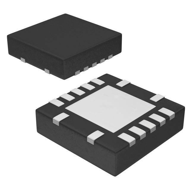
| 供应商器件封装 | 14-VQFN (3.5x3.5) |
| 其它名称 | 296-35931-6 |
| 包装 | Digi-Reel® |
| 单位重量 | 32.200 mg |
| 商标 | Texas Instruments |
| 安装类型 | 表面贴装 |
| 安装风格 | SMD/SMT |
| 封装 | Reel |
| 封装/外壳 | 14-VFQFN 裸露焊盘 |
| 封装/箱体 | VQFN-14 |
| 工作温度 | -40°C ~ 85°C |
| 工作温度范围 | - 40 C to + 125 C |
| 工厂包装数量 | 3000 |
| 最大工作温度 | + 125 C |
| 最小工作温度 | - 40 C |
| 标准包装 | 1 |
| 特性 | 施密特触发器 |
| 电压-电源 | 1.65 V ~ 3.6 V |
| 电流-输出高,低 | 24mA,24mA |
| 电流-静态(最大值) | 1µA |
| 电源电压-最大 | 3.6 V |
| 电源电压-最小 | 2 V |
| 电路数 | 6 |
| 电路数量 | 6 Circuit |
| 系列 | SN74LVC14A |
| 输入数 | 6 |
| 输入类型 | CMOS, TTL |
| 输出类型 | CMOS |
| 逻辑电平-低 | 0.15 V ~ 0.8 V |
| 逻辑电平-高 | 1.3 V ~ 2 V |
| 逻辑类型 | |
| 逻辑系列 | LVC |
| 高电平输出电流 | - 24 mA |


- 商务部:美国ITC正式对集成电路等产品启动337调查
- 曝三星4nm工艺存在良率问题 高通将骁龙8 Gen1或转产台积电
- 太阳诱电将投资9.5亿元在常州建新厂生产MLCC 预计2023年完工
- 英特尔发布欧洲新工厂建设计划 深化IDM 2.0 战略
- 台积电先进制程称霸业界 有大客户加持明年业绩稳了
- 达到5530亿美元!SIA预计今年全球半导体销售额将创下新高
- 英特尔拟将自动驾驶子公司Mobileye上市 估值或超500亿美元
- 三星加码芯片和SET,合并消费电子和移动部门,撤换高东真等 CEO
- 三星电子宣布重大人事变动 还合并消费电子和移动部门
- 海关总署:前11个月进口集成电路产品价值2.52万亿元 增长14.8%


PDF Datasheet 数据手册内容提取
Product Order Technical Tools & Support & Folder Now Documents Software Community SN54LVC14A,SN74LVC14A SCAS285AB–MARCH1993–REVISEDJULY2019 SNx4LVC14A Hex Schmitt-trigger inverters 1 Features 3 Description • Latch-upperformanceexceeds100mA The SN54LVC14A hex Schmitt-trigger inverter is 1 designed for 2.7-V to 3.6-V V operation, and the perJESD78,ClassII CC SN74LVC14Ahex Schmitt-trigger inverter is designed • ESDprotectionexceedsJESD22 for1.65-Vto3.6-VV operation. CC – 2000-Vhuman-bodymodel(A114-A) The devices contain six independent inverters and – 200-Vmachinemodel(A115-A) performtheBooleanfunctionY=A. – 1000-Vcharged-devicemodel(C101) Inputs can be driven from either 3.3-V or 5-V devices. • Operatefrom1.65Vto3.6VVCC This feature allows the use of these devices as • Specifiedfrom–40°Cto+85°C, translators in a mixed 3.3-V or 5-V system –40°Cto125°C,and –55°Cto125°C environment. • Inputsacceptvoltagesto5.5V DeviceInformation(1) • Maxt of6.4nsat3.3V pd PARTNUMBER PACKAGE BODYSIZE(NOM) • TypicalV (outputgroundbounce) OLP SN54LVC14AFK LCCC(20) 8.90mm×8.90mm <0.8VatV =3.3V,T =25°C CC A SN54LVC14AJ CDIP(14) 20.00mm×7.00mm • TypicalV (outputV undershoot) OHV OH SN54LVC14AW CFP(14) 9.21mm×6.30mm >2VatV =3.3V,T =25°C CC A SN74LVC14ANS SO(14) 10.20mm×5.30mm • OnproductscomplianttoMIL-PRF-38535, SN74LVC14AD SOIC(14) 8.65mm×6.00mm allparametersaretestedunlessotherwisenoted. SN74LVC14ADB SSOP(14) 6.20mm×5.30mm Onallotherproducts,productionprocessingdoes SN74LVC14APW TSSOP(14) 5.00mm×4.40mm notnecessarilyincludetestingofallparameters. SN74LVC14ADGV TVSOP(14) 4.40mm×3.60mm 2 Applications SN74LVC14ARGY VQFN(14) 3.50mm×3.50mm • Barcodescanner (1) For all available packages, see the orderable addendum at theendofthedatasheet. • Cablesolutions • E-books LogicDiagram(PositiveLogic) • EmbeddedPCs • Fieldtransmitter:temperatureorpressuresensors A Y • Fingerprintbiometrics • HVAC:heating,ventilating,andairconditioning • Network-attachedstorage(NAS) • ServermotherboardandPSU • Softwaredefinedradio(SDR) • TV:High-definition(HDTV),LCD,anddigital • Videocommunicationssystems • Wirelessdataaccesscards,headsets,keyboards, mice,andLANcards 1 An IMPORTANT NOTICE at the end of this data sheet addresses availability, warranty, changes, use in safety-critical applications, intellectualpropertymattersandotherimportantdisclaimers.PRODUCTIONDATA.
SN54LVC14A,SN74LVC14A SCAS285AB–MARCH1993–REVISEDJULY2019 www.ti.com Table of Contents 1 Features.................................................................. 1 8.1 Overview.................................................................10 2 Applications........................................................... 1 8.2 FunctionalBlockDiagram.......................................10 3 Description............................................................. 1 8.3 FeatureDescription.................................................10 8.4 DeviceFunctionalModes........................................11 4 RevisionHistory..................................................... 2 9 ApplicationandImplementation........................ 12 5 PinConfigurationandFunctions......................... 3 9.1 ApplicationInformation............................................12 6 Specifications......................................................... 4 9.2 TypicalApplication .................................................12 6.1 AbsoluteMaximumRatings......................................4 10 PowerSupplyRecommendations..................... 14 6.2 ESDRatings..............................................................4 11 Layout................................................................... 14 6.3 RecommendedOperatingConditions: SN54LVC14A.............................................................4 11.1 LayoutGuidelines.................................................14 6.4 RecommendedOperatingConditions: 11.2 LayoutExamples...................................................14 SN74LVC14A.............................................................5 12 DeviceandDocumentationSupport................. 15 6.5 ThermalInformation..................................................5 12.1 RelatedDocumentation.........................................15 6.6 ElectricalCharacteristics,SN54LVC14A..................5 12.2 RelatedLinks........................................................15 6.7 ElectricalCharacteristics,SN74LVC14A..................6 12.3 ReceivingNotificationofDocumentationUpdates15 6.8 SwitchingCharacteristics,SN54LVC14A.................7 12.4 CommunityResources..........................................15 6.9 SwitchingCharacteristics,SN74LVC14A.................7 12.5 Trademarks...........................................................15 6.10 OperatingCharacteristics........................................8 12.6 ElectrostaticDischargeCaution............................15 6.11 TypicalCharacteristics............................................8 12.7 Glossary................................................................15 7 ParameterMeasurementInformation..................9 13 Mechanical,Packaging,andOrderable 8 DetailedDescription............................................ 10 Information........................................................... 15 4 Revision History NOTE:Pagenumbersforpreviousrevisionsmaydifferfrompagenumbersinthecurrentversion. ChangesfromRevisionAA(June2015)toRevisionAB Page • Changedorderofthe'Features'list ...................................................................................................................................... 1 • Deleted"I SupportLiveInsertion,Partial-Power-DownModeandBackDriveprotection"fromFeatureslist.....................1 off • DeletedDeviceOptionstable,seeMechanical,Packaging,andOrderableInformationattheendofthedatasheet.........1 • AddedV >V toOutputclampcurrentinAbsoluteMaximumRatings ............................................................................. 4 O CC • ChangedMAXvalueforOutputclampcurrent,I from:–50to:±50 .................................................................................. 4 OK • ChangedvaluesintheThermalInformationtabletoalignwithJEDECstandards................................................................ 5 • AddedFeatureDescriptionsectionsforBalancedHigh-DriveCMOSPush-PullOutputs,StandardCMOSInputs, ClampDiodes,andOver-VoltageTolerantInputs............................................................................................................... 10 • AddedRelatedDocumentationandReceivingNotificationofDocumentationUpdatessections........................................ 15 ChangesfromRevisionZ(January2014)toRevisionAA Page • AddedApplications,DeviceInformationtable,PinConfigurationandFunctionssection,ESDRatingstable,Feature Descriptionsection,DeviceFunctionalModes,ApplicationandImplementationsection,PowerSupply Recommendationssection,Layoutsection,DeviceandDocumentationSupportsection,andMechanical, Packaging,andOrderableInformationsection ..................................................................................................................... 1 • MovedT toAbsoluteMaximumRatingstable..................................................................................................................... 4 stg ChangesfromRevisionY(October2010)toRevisionZ Page • UpdateddocumenttonewTIdatasheetformat.................................................................................................................... 1 • UpdatedFeatures................................................................................................................................................................... 1 • AddedMilitaryDisclaimertoFeatureslist.............................................................................................................................. 1 2 SubmitDocumentationFeedback Copyright©1993–2019,TexasInstrumentsIncorporated ProductFolderLinks:SN54LVC14A SN74LVC14A
SN54LVC14A,SN74LVC14A www.ti.com SCAS285AB–MARCH1993–REVISEDJULY2019 5 Pin Configuration and Functions D,DB,DGV,NS,J,W,orPWPackage 14-PinSOIC,SSOP,TVSOP,SO,CDIP,CFP,orTSSOP RGYPackage TopView 14-PinVQFN TopView 1A 1 14 VCC A CC 1Y 2 13 6A 1 V 1 14 2A 3 12 6Y 1Y 2 13 6A 2Y 4 11 5A 2A 3 12 6Y 3A 5 10 5Y 2Y 4 11 5A 3Y 6 9 4A 3A 5 10 5Y GND 7 8 4Y 3Y 6 9 4A 7 8 D Y N 4 G FKPackage 20-PinLCCC TopView YAC CCA 11NV 6 3 2 1 2019 2A 4 18 6Y NC 5 17 NC 2Y 6 16 5A NC 7 15 NC 3A 8 14 5Y 9 10 1112 13 YDCYA 3NN44 G PinFunctions PIN SOIC,SSOP,TVSOP,SO, I/O DESCRIPTION NAME LCCC CDIP,CFP,TSSOP,VQFN 1A 1 2 I DataInput 2A 3 4 I DataInput 3A 5 8 I DataInput 4A 9 13 I DataInput 5A 11 16 I DataInput 6A 13 19 I DataInput GND 7 10 — Ground V 14 20 — Positivesupply CC 1Y 2 3 O DataOutput 2Y 4 6 O DataOutput 3Y 6 9 O DataOutput 4Y 8 12 O DataOutput 5Y 10 14 O DataOutput 6Y 12 18 O DataOutput 1 5 7 NC — — NoConnect 11 15 17 Copyright©1993–2019,TexasInstrumentsIncorporated SubmitDocumentationFeedback 3 ProductFolderLinks:SN54LVC14A SN74LVC14A
SN54LVC14A,SN74LVC14A SCAS285AB–MARCH1993–REVISEDJULY2019 www.ti.com 6 Specifications 6.1 Absolute Maximum Ratings overoperatingfree-airtemperaturerange(unlessotherwisenoted)(1) MIN MAX UNIT V Supplyvoltage –0.5 6.5 V CC V Inputvoltage(2) –0.5 6.5 V I V Outputvoltage(2)(3) –0.5 V +0.5 V O CC I Inputclampcurrent V <0 –50 mA IK I I Outputclampcurrent V <0orV >V ±50 mA OK O O CC I Continuousoutputcurrent ±50 mA O ContinuouscurrentthroughV orGND ±100 mA CC P Powerdissipation T =–40°Cto+125°C(4)(5) 500 mW tot A T Storagetemperature –65 150 °C stg (1) StressesbeyondthoselistedunderAbsoluteMaximumRatingsmaycausepermanentdamagetothedevice.Thesearestressratings only,andfunctionaloperationofthedeviceattheseoranyotherconditionsbeyondthoseindicatedunderRecommendedOperating Conditionsisnotimplied.Exposuretoabsolute-maximum-ratedconditionsforextendedperiodsmayaffectdevicereliability. (2) Theinputandoutputnegative-voltageratingsmaybeexceedediftheinputandoutputcurrentratingsareobserved. (3) ThevalueofV isprovidedintheRecommendedOperatingConditionstable. CC (4) FortheDpackage:above70°C,thevalueofP derateslinearlywith8mW/K. tot (5) FortheDB,DGV,NS,andPWpackages:above60°C,thevalueofP derateslinearlywith5.5mW/K. tot 6.2 ESD Ratings VALUE UNIT Humanbodymodel(HBM),perANSI/ESDA/JEDECJS-001(1) +2000 V Electrostatic Charged-devicemodel(CDM),perJEDECspecificationJESD22-C101(2) +1000 V (ESD) discharge MachineModel 200 (1) JEDECdocumentJEP155statesthat500-VHBMallowssafemanufacturingwithastandardESDcontrolprocess. (2) JEDECdocumentJEP157statesthat250-VCDMallowssafemanufacturingwithastandardESDcontrolprocess. 6.3 Recommended Operating Conditions: SN54LVC14A See (1) SN54LVC14A –55TO+125°C UNIT MIN MAX Operating 2 3.6 V Supplyvoltage V CC Dataretentiononly 1.5 V Inputvoltage 0 5.5 V I V Outputvoltage 0 V V O CC V =2.7V –12 CC I High-leveloutputcurrent mA OH V =3V –24 CC V =2.7V 12 CC I Low-leveloutputcurrent mA OL V =3V 24 CC (1) AllunusedinputsofthedevicemustbeheldatV orGNDtoensureproperdeviceoperation.SeeImplicationsofSloworFloating CC CMOSInputs,SCBA004. 4 SubmitDocumentationFeedback Copyright©1993–2019,TexasInstrumentsIncorporated ProductFolderLinks:SN54LVC14A SN74LVC14A
SN54LVC14A,SN74LVC14A www.ti.com SCAS285AB–MARCH1993–REVISEDJULY2019 6.4 Recommended Operating Conditions: SN74LVC14A See (1) SN74LVC14A T =25°C –40TO+85°C –40TO+125°C UNIT A MIN MAX MIN MAX MIN MAX Operating 1.65 3.6 1.65 3.6 1.65 3.6 V Supplyvoltage V CC Dataretentiononly 1.5 1.5 1.5 V Inputvoltage 0 5.5 0 5.5 0 5.5 V I V Outputvoltage 0 V 0 V 0 V V O CC CC CC V =1.65V –4 –4 –4 CC V =2.3V –8 –8 –8 CC I High-leveloutputcurrent mA OH V =2.7V –12 –12 –12 CC V =3V –24 –24 –24 CC V =1.65V 4 4 4 CC V =2.3V 8 8 8 CC I Low-leveloutputcurrent mA OL V =2.7V 12 12 12 CC V =3V 24 24 24 CC (1) AllunusedinputsofthedevicemustbeheldatV orGNDtoensureproperdeviceoperation.SeeImplicationsofSloworFloating CC CMOSInputs,SCBA004. 6.5 Thermal Information SN74LVC14A THERMALMETRIC(1) D(SOIC) DB(SSOP) DGV(TVSOP) NS(SO) PW(TSSOP) RGY(LCCC) UNIT 14PINS 20PINS Junction-to-ambientthermal RθJA resistance 117.6 131.8 153.5 115.7 145.9 93.8 °C/W Junction-to-case(top)thermal RθJC(top) resistance 78.2 83.9 75.2 72.2 73.4 106.7 °C/W RθJB Junction-to-boardthermalresistance 71.9 79.2 86.6 74.4 87.7 69.8 °C/W Junction-to-topcharacterization ψJT parameter 39.3 41.7 19.9 33.7 18.9 22.0 °C/W Junction-to-boardcharacterization ψJB parameter 71.6 78.6 85.9 74.1 87.1 70.0 °C/W Junction-to-case(bottom)thermal RθJC(bot) resistance — — — — — 49.4 °C/W (1) Formoreinformationabouttraditionalandnewthermalmetrics,seetheSemiconductorandICPackageThermalMetricsapplication report. 6.6 Electrical Characteristics, SN54LVC14A overoperatingfree-airtemperaturerange(unlessotherwisenoted) SN54LVC14A PARAMETER TESTCONDITIONS V –55TO+125°C UNIT CC MIN TYP MAX 2.7V 0.8 2 Positive-going V 3V 0.9 2 V T+ threshold 3.6V 1.1 2 2.7V 0.4 1.4 Negative-going V 3V 0.6 1.5 V T– threshold 3.6V 0.8 1.7 2.7V 0.3 1.1 Hysteresis ΔV 3V 0.3 1.2 V T (V –V ) T+ T- 3.6V 0.3 1.2 Copyright©1993–2019,TexasInstrumentsIncorporated SubmitDocumentationFeedback 5 ProductFolderLinks:SN54LVC14A SN74LVC14A
SN54LVC14A,SN74LVC14A SCAS285AB–MARCH1993–REVISEDJULY2019 www.ti.com Electrical Characteristics, SN54LVC14A (continued) overoperatingfree-airtemperaturerange(unlessotherwisenoted) SN54LVC14A PARAMETER TESTCONDITIONS V –55TO+125°C UNIT CC MIN TYP MAX I =–100μA 2.7Vto3.6V V –0.2 OH CC 2.7V 2.2 V V V OH OL I 2.4 I I 3V 2.2 CC I =100μA 2.7Vto3.6V 0.2 OL ΔI C 2.7V 0.4 V CC i I =24mA 3V 0.55 OL V =5.5VorGND 3.6V ±5 μA I V =V orGND,I =0 3.6V 10 μA I CC O OneinputatV –0.6V, CC 2.7Vto3.6V 500 μA OtherinputsatV orGND CC V =V orGND 3.3V 5(1) pF I CC (1) T =25°C A 6.7 Electrical Characteristics, SN74LVC14A overoperatingfree-airtemperaturerange(unlessotherwisenoted) SN74LVC14A TEST PARAMETER V T =25°C –40TO+85°C –40TO+125°C UNIT CONDITIONS CC A MIN TYP MAX MIN MAX MIN MAX 1.65V 0.4 1.3 0.4 1.3 0.4 1.3 1.95V 0.6 1.5 0.6 1.5 0.6 1.5 2.3V 0.8 1.7 0.8 1.7 0.8 1.7 Positive- V going 2.5V 0.8 1.7 0.8 1.7 0.8 1.7 V T+ threshold 2.7V 0.8 2 0.8 2 0.8 2 3V 0.9 2 0.9 2 0.9 2 3.6V 1.1 2 1.1 2 1.1 2 1.65V 0.15 0.85 0.15 0.85 0.15 0.85 1.95V 0.25 0.95 0.25 0.95 0.25 0.95 2.3V 0.4 1.2 0.4 1.2 0.4 1.2 Negative- V going 2.5V 0.4 1.2 0.4 1.2 0.4 1.2 V T– threshold 2.7V 0.4 1.4 0.4 1.4 0.4 1.4 3V 0.6 1.5 0.6 1.5 0.6 1.5 3.6V 0.8 1.7 0.8 1.7 0.8 1.7 1.65V 0.1 1.15 0.1 1.15 0.1 1.15 1.95V 0.15 1.25 0.15 1.25 0.15 1.25 2.3V 0.25 1.3 0.25 1.3 0.25 1.3 Hysteresis ΔV 2.5V 0.25 1.3 0.25 1.3 0.25 1.3 V T (V –V ) T+ T- 2.7V 0.3 1.1 0.3 1.1 0.3 1.1 3V 0.3 1.2 0.3 1.2 0.3 1.2 3.6V 0.3 1.2 0.3 1.2 0.3 1.2 6 SubmitDocumentationFeedback Copyright©1993–2019,TexasInstrumentsIncorporated ProductFolderLinks:SN54LVC14A SN74LVC14A
SN54LVC14A,SN74LVC14A www.ti.com SCAS285AB–MARCH1993–REVISEDJULY2019 Electrical Characteristics, SN74LVC14A (continued) overoperatingfree-airtemperaturerange(unlessotherwisenoted) SN74LVC14A TEST PARAMETER V T =25°C –40TO+85°C –40TO+125°C UNIT CONDITIONS CC A MIN TYP MAX MIN MAX MIN MAX 1.65Vto I =–100μA V –0.2 V –0.2 V –0.3 OH 3.6V CC CC CC I =–4mA 1.65V 1.29 1.2 1.05 OH VOH IOH=–8mA 2.3V 1.9 1.7 1.65 V 2.7V 2.2 2.2 2.05 I =–12mA OH 3V 2.4 2.4 2.25 I =–24mA 3V 2.3 2.2 2 OH 1.65Vto I =100μA 0.1 0.2 0.3 OL 3.6V I =4mA 1.65V 0.24 0.45 0.6 OL V V OL I =8mA 2.3V 0.3 0.7 0.75 OL I =12mA 2.7V 0.4 0.4 0.6 OL I =24mA 3V 0.55 0.55 0.8 OL V =5.5Vor I I 3.6V ±1 ±5 ±20 μA I GND V =V or I I CC 3.6V 1 10 40 μA CC GND,I =0 O Oneinputat V –0.6V, 2.7Vto ΔI CC 500 500 5000 μA CC Otherinputsat 3.6V V orGND CC V =V or C I CC 3.3V 5 pF i GND 6.8 Switching Characteristics, SN54LVC14A overoperatingfree-airtemperaturerange(unlessotherwisenoted)(seeFigure2) SN54LVC14A FROM TO PARAMETER V –55TO+125°C UNIT (INPUT) (OUTPUT) CC MIN MAX 2.7V 7.5 t A Y ns pd 3.3V±0.3V 1 6.4 6.9 Switching Characteristics, SN74LVC14A overoperatingfree-airtemperaturerange(unlessotherwisenoted)(seeFigure2) SN74LVC14A FROM TO –40TO PARAMETER V T =25°C –40TO+85°C UNIT (INPUT) (OUTPUT) CC A +125°C MIN TYP MAX MIN MAX MIN MAX 1.8V±0.15V 1 5 10.5 1 11 1 13 2.5V±0.2V 1 3.4 7.3 1 7.8 1 10 t A Y ns pd 2.7V 1 3.6 7.3 1 7.5 1 9.5 3.3V±0.3V 1 3.2 6.2 1 6.4 1 8 t 3.3V±0.3V 1 1 1.5 ns sk(o) Copyright©1993–2019,TexasInstrumentsIncorporated SubmitDocumentationFeedback 7 ProductFolderLinks:SN54LVC14A SN74LVC14A
SN54LVC14A,SN74LVC14A SCAS285AB–MARCH1993–REVISEDJULY2019 www.ti.com 6.10 Operating Characteristics T =25°C A TEST VCC=1.8V VCC=2.5V VCC=3.3V PARAMETER UNIT CONDITIONS TYP TYP TYP C Powerdissipationcapacitance f=10MHz 11 12 15 pF pd 6.11 Typical Characteristics 16 )pd C 15 e ( c n cita 14 a p a n C 13 o ati sip 12 s Di wer 11 o P 10 1.5 1.7 1.9 2.1 2.3 2.5 2.7 2.9 3.1 3.3 3.5 Power Suppoly Voltage (VCC) D001 Figure1.PowerDissipationCapacitancevs.PowerSupplyVoltage 8 SubmitDocumentationFeedback Copyright©1993–2019,TexasInstrumentsIncorporated ProductFolderLinks:SN54LVC14A SN74LVC14A
SN54LVC14A,SN74LVC14A www.ti.com SCAS285AB–MARCH1993–REVISEDJULY2019 7 Parameter Measurement Information VLOAD From Output RL S1 Open TEST S1 Under Test GND tPLH/tPHL Open (see NoteCAL) RL tPLZ/tPZL VLOAD tPHZ/tPZH GND LOAD CIRCUIT INPUTS VCC VI tr/tf VM VLOAD CL RL VD 1.8 V±0.15 V VCC ≤2 ns VCC/2 2×VCC 30 pF 1 kW 0.15 V 2.5 V±0.2 V VCC ≤2 ns VCC/2 2×VCC 30 pF 500W 0.15 V 2.7 V 2.7 V ≤2.5 ns 1.5 V 6 V 50 pF 500W 0.3 V 3.3 V±0.3 V 2.7 V ≤2.5 ns 1.5 V 6 V 50 pF 500W 0.3 V VI Timing Input VM 0 V tw VI tsu th VI Input VM VM Data Input VM VM 0 V 0 V VOLTAGE WAVEFORMS VOLTAGE WAVEFORMS PULSE DURATION SETUPAND HOLD TIMES VI VI Output Input VM VM Control VM VM 0 V 0 V tPLH tPHL tPZL tPLZ Output VOH Waveform 1 VLOAD/2 Output VM VM VOL (Ss1ee a tN VoLteO ABD) VM VOL+ VD VOL tPHL tPLH tPZH tPHZ Output VM VM VOH WSa1v eaOftou GrtmpNu D2t VM VOH- VD VOH VOL (see Note B) ≈0 V VOLTAGE WAVEFORMS VOLTAGE WAVEFORMS PROPAGATION DELAYTIMES ENABLEAND DISABLE TIMES INVERTINGAND NONINVERTING OUTPUTS LOW-AND HIGH-LEVELENABLING NOTES: A. CLincludes probe and jig capacitance. B. Waveform 1 is for an output with internal conditions such that the output is low, except when disabled by the output control. Waveform2 is for an output with internal conditions such that the output is high, except when disabled by the output control. C. All input pulses are supplied by generators having the following characteristics: PRR≤10 MHz, ZO= 50W. D. The outputs are measured one at a time, with one transition per measurement. E. tPLZand tPHZare the same as tdis. F. tPZLand tPZHare the same as ten. G. tPLHand tPHLare the same as tpd. H. All parameters and waveforms are not applicable to all devices. Figure2. LoadCircuitandVoltageWaveforms Copyright©1993–2019,TexasInstrumentsIncorporated SubmitDocumentationFeedback 9 ProductFolderLinks:SN54LVC14A SN74LVC14A
SN54LVC14A,SN74LVC14A SCAS285AB–MARCH1993–REVISEDJULY2019 www.ti.com 8 Detailed Description 8.1 Overview The SN54LVC14A hex Schmitt-trigger inverter is designed for 2.7-V to 3.6-V V operation, and the CC SN74LVC14AhexSchmitt-triggerinverterisdesignedfor1.65-Vto3.6-VV operation. CC ThedevicescontainsixindependentinvertersandperformtheBooleanfunctionY= A. Inputs can be driven from either 3.3-V or 5-V devices. This feature allows the use of these devices as translators inamixed3.3-Vor5-Vsystemenvironment. 8.2 Functional Block Diagram A Y Figure3. LogicDiagram,EachInverter(PositiveLogic) 8.3 Feature Description 8.3.1 BalancedHigh-DriveCMOSPush-PullOutputs A balanced output allows the device to sink and source similar currents. The high drive capability of this device creates fast edges into light loads so routing and load conditions should be considered to prevent ringing. Additionally, the outputs of this device are capable of driving larger currents than the device can sustain without being damaged. It is important for the power output of the device to be limited to avoid thermal runaway and damage due to over-current. The electrical and thermal limits defined the in the Absolute Maximum Ratings must befollowedatalltimes. 8.3.2 StandardCMOSInputs Standard CMOS inputs are high impedance and are typically modelled as a resistor in parallel with the input capacitance given in the Electrical Characteristics, SN54LVC14A and Electrical Characteristics, SN74LVC14A. The worst case resistance is calculated with the maximum input voltage, given in the Absolute Maximum Ratings, and the maximum input leakage current, given in the Electrical Characteristics, SN54LVC14A and ElectricalCharacteristics,SN74LVC14A,usingohm'slaw(R=V ÷ I). Signals applied to the inputs need to have fast edge rates, as defined by Δt/Δv in Recommended Operating Conditions: SN54LVC14A and Recommended Operating Conditions: SN74LVC14A to avoid excessive currents and oscillations. If a slow or noisy input signal is required, a device with a Schmitt-trigger input should be utilized toconditiontheinputsignalpriortothestandardCMOSinput. 8.3.3 ClampDiodes The inputs to this device have negative clamping diodes. The outputs to this device have both positive and negativeclampingdiodesasshowninFigure4. CAUTION Voltages beyond the values specified in the Absolute Maximum Ratings table can cause damage to the device. The input negative-voltage and output voltage ratings maybeexceedediftheinputandoutputclamp-currentratingsareobserved. 10 SubmitDocumentationFeedback Copyright©1993–2019,TexasInstrumentsIncorporated ProductFolderLinks:SN54LVC14A SN74LVC14A
SN54LVC14A,SN74LVC14A www.ti.com SCAS285AB–MARCH1993–REVISEDJULY2019 Feature Description (continued) Device VCC +IOK Input Logic Output -IIK -IOK GND Figure4. ElectricalPlacementofClampingDiodesforEachInputandOutput 8.3.4 Over-voltageTolerantInputs Input signals to this device can be driven above the supply voltage so long as they remain below the maximum inputvoltagevaluespecifiedintheAbsoluteMaximumRatings. 8.4 Device Functional Modes Table1liststhefunctionalmodesfortheSN54LVC14AandSN74LVC14Adevices. Table1.FunctionTable(EachInverter) INPUT OUTPUT A Y H L L H Copyright©1993–2019,TexasInstrumentsIncorporated SubmitDocumentationFeedback 11 ProductFolderLinks:SN54LVC14A SN74LVC14A
SN54LVC14A,SN74LVC14A SCAS285AB–MARCH1993–REVISEDJULY2019 www.ti.com 9 Application and Implementation NOTE Information in the following applications sections is not part of the TI component specification, and TI does not warrant its accuracy or completeness. TI’s customers are responsible for determining suitability of components for their purposes. Customers should validateandtesttheirdesignimplementationtoconfirmsystemfunctionality. 9.1 Application Information Physically interactive interface elements like push buttons or rotary knobs offer simple and easy ways to interact with an electronic system. Many of these physical interface elements often have issues with bouncing, or where the physical conductive contact can connect and disconnect multiple times during a button push or release. This bouncing can cause one or more faulty transient signals to be passed during this transitional period. These faulty signals can be observed in many common applications: for example, a television remote with bouncing error can adjust the TV channel multiple times despite the button being pushed only once. To mitigate these faulty signals, use a Schmitt-trigger, or a device with hysteresis, to remove these faulty signals. Hysteresis allows a device to "remember" its history, and in this case, the LVC14A uses this memory to debounce the physical element's signal, or filter the faulty transient signals and pass only the valid signal each time the element is used. In this example, we show a push button signal passed through an LVC14A that is debounced and inverted to the MCU forpushdetection. 9.2 Typical Application The signal effects of the debounce circuit can be seen when comparing Figure 6 and Figure 7. In Figure 6, the input is a very poor quality signal due to the error in the physical push button. If the MCU attempts to sample this input to detect a push, there is high probability that multiple push events will be falsely detected. Once the debounce circuit has been implemented, the input is cleaned up, and the MCU can perform push detection withoutanyerror,asseeninFigure7. V = 3.3 V CC GND V CC LVC14A MCU Push Button (MSP43x) 1A 1Y (x6) Copyright © 2017, Texas Instruments Incorporated Figure5. DebouncerApplicationDiagram 9.2.1 DesignRequirements The SN74LVC14A device uses CMOS technology and has balanced output drive. Take care to avoid bus contentionbecauseitcandrivecurrentsthatwouldexceedmaximumlimits. The SN74LVC14A allows for performing logical Boolean functions with hysteresis using digital signals. All input signalsshouldremainascloseaspossibletoeither0VorV foroptimaloperation. CC 12 SubmitDocumentationFeedback Copyright©1993–2019,TexasInstrumentsIncorporated ProductFolderLinks:SN54LVC14A SN74LVC14A
SN54LVC14A,SN74LVC14A www.ti.com SCAS285AB–MARCH1993–REVISEDJULY2019 Typical Application (continued) 9.2.2 DetailedDesignProcedure 1. Recommendedinputconditions: – For rise time and fall time specifications, see Δt/Δv in the Recommended Operating Conditions: SN74LVC14Atable. – For specified high and low levels, see V and V in the Recommended Operating Conditions: IH IL SN74LVC14Atable. – Inputsandoutputsareovervoltagetolerantandcanthereforegoashighas3.6VatanyvalidV . CC 2. Recommendedoutputconditions: – Loadcurrentsshouldnotexceed ±50mA. 3. Frequencyselectioncriterion: – Added trace resistance and capacitance can reduce maximum frequency capability; follow the layout practiceslistedinthesection. 9.2.3 ApplicationCurves V V BUT BUT t t Figure6.InputResponseWithoutDebounceCircuit Figure7.InputResponseWithDebounceCircuit Copyright©1993–2019,TexasInstrumentsIncorporated SubmitDocumentationFeedback 13 ProductFolderLinks:SN54LVC14A SN74LVC14A
SN54LVC14A,SN74LVC14A SCAS285AB–MARCH1993–REVISEDJULY2019 www.ti.com 10 Power Supply Recommendations The power supply can be any voltage between the minimum and maximum supply voltage rating listed in the table. Each V terminal should have a good bypass capacitor to prevent power disturbance. For devices with a single CC supply, a 0.1-µF bypass capacitor is recommended. If multiple pins are labeled V , then a 0.01-µF or 0.022-µF CC capacitor is recommended for each V because the V pins are tied together internally. For devices with dual CC CC supply pins operating at different voltages, for example V and V , a 0.1-µF bypass capacitor is recommended CC DD foreachsupplypin.Torejectdifferentfrequenciesofnoise,usemultiplebypasscapacitorsin parallel. Capacitors with values of 0.1 µF and 1 µF are commonly used in parallel. The bypass capacitor should be installed as close tothepowerterminalaspossibleforbestresults. 11 Layout 11.1 Layout Guidelines Whenusingmultiple-bitlogicdevices,inputsmustneverfloat. In many cases, functions (or parts of functions) of digital logic devices are unused, for example, when only two inputs of a triple-input AND gate are used or when only 3 of the 4 buffer gates are used. Such input pins must not be left unconnected, because the undefined voltages at the outside connections result in undefined operational states. Figure 8 specifies the rules that must be observed under all circumstances. All unused inputs of digital logic devices must be connected to a high or low bias to prevent them from floating. The logic level that must be applied to any particular unused input depends on the function of the device. Generally they are tied to GND or V , whichever makes more sense or is more convenient. It is generally acceptable to float outputs, CC unless the part is a transceiver. If the transceiver has an output enable pin, it disables the output section of the part when asserted, which does not disable the input section of the I/Os. Therefore, the I/Os cannot float when disabled. 11.2 Layout Examples V cc Input Unused Input Output Unused Input Output Input Figure8. LayoutDiagrams 14 SubmitDocumentationFeedback Copyright©1993–2019,TexasInstrumentsIncorporated ProductFolderLinks:SN54LVC14A SN74LVC14A
SN54LVC14A,SN74LVC14A www.ti.com SCAS285AB–MARCH1993–REVISEDJULY2019 12 Device and Documentation Support 12.1 Related Documentation Forrelateddocumentationseethefollowing: ImplicationsofSloworFloatingCMOSInputs,SCBA004. 12.2 Related Links The table below lists quick access links. Categories include technical documents, support and community resources,toolsandsoftware,andquickaccesstoordernow. Table2.RelatedLinks TECHNICAL TOOLS& SUPPORT& PARTS PRODUCTFOLDER ORDERNOW DOCUMENTS SOFTWARE COMMUNITY SN54LVC14A Clickhere Clickhere Clickhere Clickhere Clickhere SN74LVC14A Clickhere Clickhere Clickhere Clickhere Clickhere 12.3 Receiving Notification of Documentation Updates To receive notification of documentation updates, navigate to the device product folder on ti.com. In the upper right corner, click on Alert me to register and receive a weekly digest of any product information that has changed.Forchangedetails,reviewtherevisionhistoryincludedinanyreviseddocument. 12.4 Community Resources The following links connect to TI community resources. Linked contents are provided "AS IS" by the respective contributors. They do not constitute TI specifications and do not necessarily reflect TI's views; see TI's Terms of Use. TIE2E™OnlineCommunity TI'sEngineer-to-Engineer(E2E)Community.Createdtofostercollaboration amongengineers.Ate2e.ti.com,youcanaskquestions,shareknowledge,exploreideasandhelp solveproblemswithfellowengineers. DesignSupport TI'sDesignSupport QuicklyfindhelpfulE2Eforumsalongwithdesignsupporttoolsand contactinformationfortechnicalsupport. 12.5 Trademarks E2EisatrademarkofTexasInstruments. Allothertrademarksarethepropertyoftheirrespectiveowners. 12.6 Electrostatic Discharge Caution Thesedeviceshavelimitedbuilt-inESDprotection.Theleadsshouldbeshortedtogetherorthedeviceplacedinconductivefoam duringstorageorhandlingtopreventelectrostaticdamagetotheMOSgates. 12.7 Glossary SLYZ022—TIGlossary. Thisglossarylistsandexplainsterms,acronyms,anddefinitions. 13 Mechanical, Packaging, and Orderable Information The following pages include mechanical packaging and orderable information. This information is the most current data available for the designated devices. This data is subject to change without notice and revision of thisdocument.Forbrowserbasedversionsofthisdatasheet,refertothelefthandnavigation. Copyright©1993–2019,TexasInstrumentsIncorporated SubmitDocumentationFeedback 15 ProductFolderLinks:SN54LVC14A SN74LVC14A
PACKAGE OPTION ADDENDUM www.ti.com 6-Feb-2020 PACKAGING INFORMATION Orderable Device Status Package Type Package Pins Package Eco Plan Lead/Ball Finish MSL Peak Temp Op Temp (°C) Device Marking Samples (1) Drawing Qty (2) (6) (3) (4/5) 5962-9761501Q2A ACTIVE LCCC FK 20 1 TBD POST-PLATE N / A for Pkg Type -55 to 125 5962- 9761501Q2A SNJ54LVC 14AFK 5962-9761501QCA ACTIVE CDIP J 14 1 TBD Call TI N / A for Pkg Type -55 to 125 5962-9761501QC A SNJ54LVC14AJ 5962-9761501QDA ACTIVE CFP W 14 1 TBD Call TI N / A for Pkg Type -55 to 125 5962-9761501QD A SNJ54LVC14AW 5962-9761501V2A ACTIVE LCCC FK 20 1 TBD POST-PLATE N / A for Pkg Type -55 to 125 5962- 9761501V2A SNV54LVC 14AFK 5962-9761501VCA ACTIVE CDIP J 14 1 TBD Call TI N / A for Pkg Type -55 to 125 5962-9761501VC A SNV54LVC14AJ 5962-9761501VDA ACTIVE CFP W 14 1 TBD Call TI N / A for Pkg Type -55 to 125 5962-9761501VD A SNV54LVC14AW SN74LVC14AD ACTIVE SOIC D 14 50 Green (RoHS NIPDAU Level-1-260C-UNLIM -40 to 125 LVC14A & no Sb/Br) SN74LVC14ADBR ACTIVE SSOP DB 14 2000 Green (RoHS NIPDAU Level-1-260C-UNLIM -40 to 125 LC14A & no Sb/Br) SN74LVC14ADBRE4 ACTIVE SSOP DB 14 2000 Green (RoHS NIPDAU Level-1-260C-UNLIM -40 to 125 LC14A & no Sb/Br) SN74LVC14ADE4 ACTIVE SOIC D 14 50 Green (RoHS NIPDAU Level-1-260C-UNLIM -40 to 125 LVC14A & no Sb/Br) SN74LVC14ADG4 ACTIVE SOIC D 14 50 Green (RoHS NIPDAU Level-1-260C-UNLIM -40 to 125 LVC14A & no Sb/Br) SN74LVC14ADGVR ACTIVE TVSOP DGV 14 2000 Green (RoHS NIPDAU Level-1-260C-UNLIM -40 to 125 LC14A & no Sb/Br) SN74LVC14ADR ACTIVE SOIC D 14 2500 Green (RoHS NIPDAU | SN Level-1-260C-UNLIM -40 to 125 LVC14A & no Sb/Br) Addendum-Page 1
PACKAGE OPTION ADDENDUM www.ti.com 6-Feb-2020 Orderable Device Status Package Type Package Pins Package Eco Plan Lead/Ball Finish MSL Peak Temp Op Temp (°C) Device Marking Samples (1) Drawing Qty (2) (6) (3) (4/5) SN74LVC14ADRE4 ACTIVE SOIC D 14 2500 Green (RoHS NIPDAU Level-1-260C-UNLIM -40 to 125 LVC14A & no Sb/Br) SN74LVC14ADRG3 ACTIVE SOIC D 14 2500 Green (RoHS SN Level-1-260C-UNLIM -40 to 125 LVC14A & no Sb/Br) SN74LVC14ADRG4 ACTIVE SOIC D 14 2500 Green (RoHS NIPDAU Level-1-260C-UNLIM -40 to 125 LVC14A & no Sb/Br) SN74LVC14ADT ACTIVE SOIC D 14 250 Green (RoHS NIPDAU Level-1-260C-UNLIM -40 to 125 LVC14A & no Sb/Br) SN74LVC14ANSR ACTIVE SO NS 14 2000 Green (RoHS NIPDAU Level-1-260C-UNLIM -40 to 125 LVC14A & no Sb/Br) SN74LVC14APW ACTIVE TSSOP PW 14 90 Green (RoHS NIPDAU Level-1-260C-UNLIM -40 to 125 LC14A & no Sb/Br) SN74LVC14APWG4 ACTIVE TSSOP PW 14 90 Green (RoHS NIPDAU Level-1-260C-UNLIM -40 to 125 LC14A & no Sb/Br) SN74LVC14APWR ACTIVE TSSOP PW 14 2000 Green (RoHS NIPDAU | SN Level-1-260C-UNLIM -40 to 125 LC14A & no Sb/Br) SN74LVC14APWRE4 ACTIVE TSSOP PW 14 2000 Green (RoHS NIPDAU Level-1-260C-UNLIM -40 to 125 LC14A & no Sb/Br) SN74LVC14APWRG3 ACTIVE TSSOP PW 14 2000 Green (RoHS SN Level-1-260C-UNLIM -40 to 125 LC14A & no Sb/Br) SN74LVC14APWRG4 ACTIVE TSSOP PW 14 2000 Green (RoHS NIPDAU Level-1-260C-UNLIM -40 to 125 LC14A & no Sb/Br) SN74LVC14APWT ACTIVE TSSOP PW 14 250 Green (RoHS NIPDAU Level-1-260C-UNLIM -40 to 125 LC14A & no Sb/Br) SN74LVC14APWTG4 ACTIVE TSSOP PW 14 250 Green (RoHS NIPDAU Level-1-260C-UNLIM -40 to 125 LC14A & no Sb/Br) SN74LVC14ARGYR ACTIVE VQFN RGY 14 3000 Green (RoHS NIPDAU Level-2-260C-1 YEAR -40 to 125 LC14A & no Sb/Br) SN74LVC14ARGYRG4 ACTIVE VQFN RGY 14 3000 Green (RoHS NIPDAU Level-2-260C-1 YEAR -40 to 125 LC14A & no Sb/Br) SNJ54LVC14AFK ACTIVE LCCC FK 20 1 TBD POST-PLATE N / A for Pkg Type -55 to 125 5962- 9761501Q2A SNJ54LVC 14AFK SNJ54LVC14AJ ACTIVE CDIP J 14 1 TBD Call TI N / A for Pkg Type -55 to 125 5962-9761501QC A SNJ54LVC14AJ Addendum-Page 2
PACKAGE OPTION ADDENDUM www.ti.com 6-Feb-2020 Orderable Device Status Package Type Package Pins Package Eco Plan Lead/Ball Finish MSL Peak Temp Op Temp (°C) Device Marking Samples (1) Drawing Qty (2) (6) (3) (4/5) SNJ54LVC14AW ACTIVE CFP W 14 1 TBD Call TI N / A for Pkg Type -55 to 125 5962-9761501QD A SNJ54LVC14AW (1) The marketing status values are defined as follows: ACTIVE: Product device recommended for new designs. LIFEBUY: TI has announced that the device will be discontinued, and a lifetime-buy period is in effect. NRND: Not recommended for new designs. Device is in production to support existing customers, but TI does not recommend using this part in a new design. PREVIEW: Device has been announced but is not in production. Samples may or may not be available. OBSOLETE: TI has discontinued the production of the device. (2) RoHS: TI defines "RoHS" to mean semiconductor products that are compliant with the current EU RoHS requirements for all 10 RoHS substances, including the requirement that RoHS substance do not exceed 0.1% by weight in homogeneous materials. Where designed to be soldered at high temperatures, "RoHS" products are suitable for use in specified lead-free processes. TI may reference these types of products as "Pb-Free". RoHS Exempt: TI defines "RoHS Exempt" to mean products that contain lead but are compliant with EU RoHS pursuant to a specific EU RoHS exemption. Green: TI defines "Green" to mean the content of Chlorine (Cl) and Bromine (Br) based flame retardants meet JS709B low halogen requirements of <=1000ppm threshold. Antimony trioxide based flame retardants must also meet the <=1000ppm threshold requirement. (3) MSL, Peak Temp. - The Moisture Sensitivity Level rating according to the JEDEC industry standard classifications, and peak solder temperature. (4) There may be additional marking, which relates to the logo, the lot trace code information, or the environmental category on the device. (5) Multiple Device Markings will be inside parentheses. Only one Device Marking contained in parentheses and separated by a "~" will appear on a device. If a line is indented then it is a continuation of the previous line and the two combined represent the entire Device Marking for that device. (6) Lead/Ball Finish - Orderable Devices may have multiple material finish options. Finish options are separated by a vertical ruled line. Lead/Ball Finish values may wrap to two lines if the finish value exceeds the maximum column width. Important Information and Disclaimer:The information provided on this page represents TI's knowledge and belief as of the date that it is provided. TI bases its knowledge and belief on information provided by third parties, and makes no representation or warranty as to the accuracy of such information. Efforts are underway to better integrate information from third parties. TI has taken and continues to take reasonable steps to provide representative and accurate information but may not have conducted destructive testing or chemical analysis on incoming materials and chemicals. TI and TI suppliers consider certain information to be proprietary, and thus CAS numbers and other limited information may not be available for release. In no event shall TI's liability arising out of such information exceed the total purchase price of the TI part(s) at issue in this document sold by TI to Customer on an annual basis. OTHER QUALIFIED VERSIONS OF SN54LVC14A, SN54LVC14A-SP, SN74LVC14A : Addendum-Page 3
PACKAGE OPTION ADDENDUM www.ti.com 6-Feb-2020 •Catalog: SN74LVC14A, SN54LVC14A •Automotive: SN74LVC14A-Q1, SN74LVC14A-Q1 •Enhanced Product: SN74LVC14A-EP, SN74LVC14A-EP •Military: SN54LVC14A •Space: SN54LVC14A-SP NOTE: Qualified Version Definitions: •Catalog - TI's standard catalog product •Automotive - Q100 devices qualified for high-reliability automotive applications targeting zero defects •Enhanced Product - Supports Defense, Aerospace and Medical Applications •Military - QML certified for Military and Defense Applications •Space - Radiation tolerant, ceramic packaging and qualified for use in Space-based application Addendum-Page 4
PACKAGE MATERIALS INFORMATION www.ti.com 20-Dec-2018 TAPE AND REEL INFORMATION *Alldimensionsarenominal Device Package Package Pins SPQ Reel Reel A0 B0 K0 P1 W Pin1 Type Drawing Diameter Width (mm) (mm) (mm) (mm) (mm) Quadrant (mm) W1(mm) SN74LVC14ADGVR TVSOP DGV 14 2000 330.0 12.4 6.8 4.0 1.6 8.0 12.0 Q1 SN74LVC14ADR SOIC D 14 2500 330.0 16.4 6.5 9.0 2.1 8.0 16.0 Q1 SN74LVC14ADR SOIC D 14 2500 330.0 16.4 6.5 9.0 2.1 8.0 16.0 Q1 SN74LVC14ADR SOIC D 14 2500 330.0 16.8 6.5 9.5 2.1 8.0 16.0 Q1 SN74LVC14ADRG3 SOIC D 14 2500 330.0 16.8 6.5 9.5 2.1 8.0 16.0 Q1 SN74LVC14ADRG4 SOIC D 14 2500 330.0 16.4 6.5 9.0 2.1 8.0 16.0 Q1 SN74LVC14ADRG4 SOIC D 14 2500 330.0 16.4 6.5 9.0 2.1 8.0 16.0 Q1 SN74LVC14ADT SOIC D 14 250 330.0 16.4 6.5 9.0 2.1 8.0 16.0 Q1 SN74LVC14ANSR SO NS 14 2000 330.0 16.4 8.2 10.5 2.5 12.0 16.0 Q1 SN74LVC14APWR TSSOP PW 14 2000 330.0 12.4 6.9 5.6 1.6 8.0 12.0 Q1 SN74LVC14APWR TSSOP PW 14 2000 330.0 12.4 6.9 5.6 1.6 8.0 12.0 Q1 SN74LVC14APWRG3 TSSOP PW 14 2000 330.0 12.4 6.9 5.6 1.6 8.0 12.0 Q1 SN74LVC14APWRG4 TSSOP PW 14 2000 330.0 12.4 6.9 5.6 1.6 8.0 12.0 Q1 SN74LVC14APWT TSSOP PW 14 250 330.0 12.4 6.9 5.6 1.6 8.0 12.0 Q1 SN74LVC14ARGYR VQFN RGY 14 3000 330.0 12.4 3.75 3.75 1.15 8.0 12.0 Q1 PackMaterials-Page1
PACKAGE MATERIALS INFORMATION www.ti.com 20-Dec-2018 *Alldimensionsarenominal Device PackageType PackageDrawing Pins SPQ Length(mm) Width(mm) Height(mm) SN74LVC14ADGVR TVSOP DGV 14 2000 367.0 367.0 35.0 SN74LVC14ADR SOIC D 14 2500 333.2 345.9 28.6 SN74LVC14ADR SOIC D 14 2500 367.0 367.0 38.0 SN74LVC14ADR SOIC D 14 2500 364.0 364.0 27.0 SN74LVC14ADRG3 SOIC D 14 2500 364.0 364.0 27.0 SN74LVC14ADRG4 SOIC D 14 2500 333.2 345.9 28.6 SN74LVC14ADRG4 SOIC D 14 2500 367.0 367.0 38.0 SN74LVC14ADT SOIC D 14 250 210.0 185.0 35.0 SN74LVC14ANSR SO NS 14 2000 367.0 367.0 38.0 SN74LVC14APWR TSSOP PW 14 2000 367.0 367.0 35.0 SN74LVC14APWR TSSOP PW 14 2000 364.0 364.0 27.0 SN74LVC14APWRG3 TSSOP PW 14 2000 364.0 364.0 27.0 SN74LVC14APWRG4 TSSOP PW 14 2000 367.0 367.0 35.0 SN74LVC14APWT TSSOP PW 14 250 367.0 367.0 35.0 SN74LVC14ARGYR VQFN RGY 14 3000 367.0 367.0 35.0 PackMaterials-Page2
None
None
None
None
None
None
MECHANICAL DATA MPDS006C – FEBRUARY 1996 – REVISED AUGUST 2000 DGV (R-PDSO-G**) PLASTIC SMALL-OUTLINE 24 PINS SHOWN 0,23 0,40 0,07 M 0,13 24 13 0,16 NOM 4,50 6,60 4,30 6,20 Gage Plane 0,25 0°–(cid:1)8° 0,75 1 12 0,50 A Seating Plane 0,15 1,20 MAX 0,08 0,05 PINS ** 14 16 20 24 38 48 56 DIM A MAX 3,70 3,70 5,10 5,10 7,90 9,80 11,40 A MIN 3,50 3,50 4,90 4,90 7,70 9,60 11,20 4073251/E 08/00 NOTES: A. All linear dimensions are in millimeters. B. This drawing is subject to change without notice. C. Body dimensions do not include mold flash or protrusion, not to exceed 0,15 per side. D. Falls within JEDEC: 24/48 Pins – MO-153 14/16/20/56 Pins – MO-194 • POST OFFICE BOX 655303 DALLAS, TEXAS 75265
None
PACKAGE OUTLINE J0014A CDIP - 5.08 mm max height SCALE 0.900 CERAMIC DUAL IN LINE PACKAGE PIN 1 ID A 4X .005 MIN (OPTIONAL) [0.13] .015-.060 TYP [0.38-1.52] 1 14 12X .100 [2.54] 14X .014-.026 14X .045-.065 [0.36-0.66] [1.15-1.65] .010 [0.25] C A B .754-.785 [19.15-19.94] 7 8 B .245-.283 .2 MAX TYP .13 MIN TYP [6.22-7.19] [5.08] [3.3] SEATING PLANE C .308-.314 [7.83-7.97] AT GAGE PLANE .015 GAGE PLANE [0.38] 0 -15 14X .008-.014 TYP [0.2-0.36] 4214771/A 05/2017 NOTES: 1. All controlling linear dimensions are in inches. Dimensions in brackets are in millimeters. Any dimension in brackets or parenthesis are for reference only. Dimensioning and tolerancing per ASME Y14.5M. 2. This drawing is subject to change without notice. 3. This package is hermitically sealed with a ceramic lid using glass frit. 4. Index point is provided on cap for terminal identification only and on press ceramic glass frit seal only. 5. Falls within MIL-STD-1835 and GDIP1-T14. www.ti.com
EXAMPLE BOARD LAYOUT J0014A CDIP - 5.08 mm max height CERAMIC DUAL IN LINE PACKAGE (.300 ) TYP [7.62] SEE DETAIL B SEE DETAIL A 1 14 12X (.100 ) [2.54] SYMM 14X ( .039) [1] 7 8 SYMM LAND PATTERN EXAMPLE NON-SOLDER MASK DEFINED SCALE: 5X .002 MAX (.063) [0.05] [1.6] METAL ALL AROUND ( .063) SOLDER MASK [1.6] OPENING METAL .002 MAX SOLDER MASK (R.002 ) TYP [0.05] OPENING [0.05] ALL AROUND DETAIL A DETAIL B SCALE: 15X 13X, SCALE: 15X 4214771/A 05/2017 www.ti.com
None
None
None
None
MECHANICAL DATA MSSO002E – JANUARY 1995 – REVISED DECEMBER 2001 DB (R-PDSO-G**) PLASTIC SMALL-OUTLINE 28 PINS SHOWN 0,38 0,65 0,15 M 0,22 28 15 0,25 0,09 5,60 8,20 5,00 7,40 Gage Plane 1 14 0,25 A 0°–(cid:1)8° 0,95 0,55 Seating Plane 2,00 MAX 0,05 MIN 0,10 PINS ** 14 16 20 24 28 30 38 DIM A MAX 6,50 6,50 7,50 8,50 10,50 10,50 12,90 A MIN 5,90 5,90 6,90 7,90 9,90 9,90 12,30 4040065/E 12/01 NOTES: A. All linear dimensions are in millimeters. B. This drawing is subject to change without notice. C. Body dimensions do not include mold flash or protrusion not to exceed 0,15. D. Falls within JEDEC MO-150 • POST OFFICE BOX 655303 DALLAS, TEXAS 75265
IMPORTANTNOTICEANDDISCLAIMER TI PROVIDES TECHNICAL AND RELIABILITY DATA (INCLUDING DATASHEETS), DESIGN RESOURCES (INCLUDING REFERENCE DESIGNS), APPLICATION OR OTHER DESIGN ADVICE, WEB TOOLS, SAFETY INFORMATION, AND OTHER RESOURCES “AS IS” AND WITH ALL FAULTS, AND DISCLAIMS ALL WARRANTIES, EXPRESS AND IMPLIED, INCLUDING WITHOUT LIMITATION ANY IMPLIED WARRANTIES OF MERCHANTABILITY, FITNESS FOR A PARTICULAR PURPOSE OR NON-INFRINGEMENT OF THIRD PARTY INTELLECTUAL PROPERTY RIGHTS. These resources are intended for skilled developers designing with TI products. You are solely responsible for (1) selecting the appropriate TI products for your application, (2) designing, validating and testing your application, and (3) ensuring your application meets applicable standards, and any other safety, security, or other requirements. These resources are subject to change without notice. TI grants you permission to use these resources only for development of an application that uses the TI products described in the resource. Other reproduction and display of these resources is prohibited. No license is granted to any other TI intellectual property right or to any third party intellectual property right. TI disclaims responsibility for, and you will fully indemnify TI and its representatives against, any claims, damages, costs, losses, and liabilities arising out of your use of these resources. TI’s products are provided subject to TI’s Terms of Sale (www.ti.com/legal/termsofsale.html) or other applicable terms available either on ti.com or provided in conjunction with such TI products. TI’s provision of these resources does not expand or otherwise alter TI’s applicable warranties or warranty disclaimers for TI products. Mailing Address: Texas Instruments, Post Office Box 655303, Dallas, Texas 75265 Copyright © 2020, Texas Instruments Incorporated