ICGOO在线商城 > 集成电路(IC) > 接口 - 模拟开关,多路复用器,多路分解器 > SN74LV4051ARGYR
 Datasheet下载
- 型号: SN74LV4051ARGYR
- 制造商: Texas Instruments
- 库位|库存: xxxx|xxxx
- 要求:
| 数量阶梯 | 香港交货 | 国内含税 |
| +xxxx | $xxxx | ¥xxxx |
查看当月历史价格
查看今年历史价格
SN74LV4051ARGYR产品简介:
ICGOO电子元器件商城为您提供SN74LV4051ARGYR由Texas Instruments设计生产,在icgoo商城现货销售,并且可以通过原厂、代理商等渠道进行代购。 SN74LV4051ARGYR价格参考。Texas InstrumentsSN74LV4051ARGYR封装/规格:接口 - 模拟开关,多路复用器,多路分解器, 1 Circuit IC Switch 8:1 75 Ohm 16-VQFN (4x4)。您可以下载SN74LV4051ARGYR参考资料、Datasheet数据手册功能说明书,资料中有SN74LV4051ARGYR 详细功能的应用电路图电压和使用方法及教程。
SN74LV4051ARGYR 是德州仪器(Texas Instruments)生产的一款8通道模拟开关/多路复用器。该器件具有低导通电阻、低功耗和宽电源电压范围等特性,适用于多种模拟信号处理和控制应用场景。以下是其主要应用场景:

 1. 数据采集系统
   SN74LV4051ARGYR 可用于数据采集系统中,作为多路复用器来选择多个传感器或信号源中的一个进行采样。例如,在工业自动化、环境监测或医疗设备中,多个温度、压力或生物电信号传感器可以通过该器件分时复用到单个ADC(模数转换器),从而简化电路设计并降低成本。

 2. 音频信号切换
   在音频设备中,如混音台、耳机放大器或多声道音响系统,SN74LV4051ARGYR 可以用来在多个音频输入源之间进行切换。它能够确保音频信号的低失真传输,同时提供灵活的通道选择功能,适用于家庭影院、车载娱乐系统等场景。

 3. 传感器接口
   对于需要连接多个传感器的应用,如智能家居、物联网设备或机器人控制系统,SN74LV4051ARGYR 可以有效地管理多个传感器的输入信号。通过多路复用,它可以减少对外围接口的需求,简化PCB布局,并提高系统的集成度。

 4. 测试与测量设备
   在测试与测量领域,如示波器、信号发生器或多通道测量仪中,SN74LV4051ARGYR 可用于选择不同的测量通道或信号源。它的低导通电阻和高线性度确保了测量结果的准确性,同时其快速切换速度支持高频信号的实时监测。

 5. 通信系统
   在某些通信设备中,如无线收发模块或多频段天线切换,SN74LV4051ARGYR 可以作为信号路径的选择器,帮助实现不同频段或信道之间的快速切换。这有助于提高通信系统的灵活性和效率。

 总结
SN74LV4051ARGYR 凭借其出色的性能和广泛的适用性,成为模拟信号处理、数据采集、音频切换、传感器管理和测试测量等领域的理想选择。其低功耗和紧凑封装也使得它非常适合便携式和电池供电的应用场景。
| 参数 | 数值 |
| 产品目录 | 集成电路 (IC)半导体 |
| 描述 | IC MUX/DEMUX 8X1 16VQFN多路器开关 IC 8-Channel Analog |
| 产品分类 | |
| 品牌 | Texas Instruments |
| 产品手册 | |
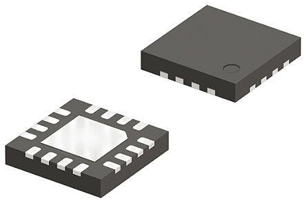
| 产品图片 |
|
| rohs | 符合RoHS无铅 / 符合限制有害物质指令(RoHS)规范要求 |
| 产品系列 | 开关 IC,多路器开关 IC,Texas Instruments SN74LV4051ARGYR74LV |
| 数据手册 | |
| 产品型号 | SN74LV4051ARGYR |
| PCN设计/规格 | |
| 产品种类 | 多路器开关 IC |
| 传播延迟时间 | 7 ns |
| 供应商器件封装 | 16-VQFN(4x4) |
| 其它名称 | 296-13945-6 |
| 功能 | 多路复用器/多路分解器 |
| 包装 | Digi-Reel® |
| 单位重量 | 37.200 mg |
| 商标 | Texas Instruments |
| 安装类型 | 表面贴装 |
| 安装风格 | SMD/SMT |
| 导通电阻 | 75 欧姆 |
| 导通电阻—最大值 | 75 Ohms |
| 封装 | Reel |
| 封装/外壳 | 16-VFQFN 裸露焊盘 |
| 封装/箱体 | VQFN-16 |
| 工作温度 | -40°C ~ 85°C |
| 工作电源电压 | 2 V to 5.5 V |
| 工作电源电流 | 20 uA |
| 工厂包装数量 | 3000 |
| 带宽 | 35 Mhz |
| 开关配置 | 1 X 1:8 MUX |
| 最大工作温度 | + 85 C |
| 最小工作温度 | - 40 C |
| 标准包装 | 1 |
| 电压-电源,单/双 (±) | 2 V ~ 5.5 V |
| 电压源 | 单电源 |
| 电流-电源 | 20µA |
| 电路 | 1 x 8:1 |
| 空闲时间—最大值 | 28 ns |
| 系列 | SN74LV4051A |
| 运行时间—最大值 | 28 ns |
| 通道数量 | 8 Channel |


- 商务部:美国ITC正式对集成电路等产品启动337调查
- 曝三星4nm工艺存在良率问题 高通将骁龙8 Gen1或转产台积电
- 太阳诱电将投资9.5亿元在常州建新厂生产MLCC 预计2023年完工
- 英特尔发布欧洲新工厂建设计划 深化IDM 2.0 战略
- 台积电先进制程称霸业界 有大客户加持明年业绩稳了
- 达到5530亿美元!SIA预计今年全球半导体销售额将创下新高
- 英特尔拟将自动驾驶子公司Mobileye上市 估值或超500亿美元
- 三星加码芯片和SET,合并消费电子和移动部门,撤换高东真等 CEO
- 三星电子宣布重大人事变动 还合并消费电子和移动部门
- 海关总署:前11个月进口集成电路产品价值2.52万亿元 增长14.8%


PDF Datasheet 数据手册内容提取
Product Sample & Technical Tools & Support & Folder Buy Documents Software Community SN74LV4051A SCLS428I–MAY1999–REVISEDSEPTEMBER2015 SN74LV4051A 8-Channel Analog Multiplexers and Demultiplexers 1 Features 3 Description • 2-Vto5.5-VV Operation The SN74LV4051A 8-channel CMOS analog 1 CC multiplexers and demultiplexers are designed for 2-V • SupportMixed-ModeVoltageOperationon to5.5-VV operation. AllPorts CC The SN74LV4051A devices handle both analog and • HighOn-OffOutput-VoltageRatio digital signals. Each channel permits signals with • LowCrosstalkBetweenSwitches amplitudes up to 5.5-V (peak) to be transmitted in • IndividualSwitchControls eitherdirection. • ExtremelyLowInputCurrent Applications include: signal gating, chopping, • Latch-UpPerformanceExceeds100-mAPer modulation or demodulation (modem), and signal JESD78,ClassII multiplexing for analog-to-digital and digital-to-analog conversionsystems. • ESDProtectionExceedsJESD22 – 2000-VHuman-BodyModel(A114-A) DeviceInformation(1) – 200-VMachineModel(A115-A) PARTNUMBER PACKAGE BODYSIZE(NOM) – 1000-VCharged-DeviceModel(C101) TSSOP(16) 5.00mm×6.30mm SOIC(16) 9.90mm×6.00mm 2 Applications SSOP(16) 6.20mm×7.80mm • Telecommunications SN74LV4051A TVSOP(16) 3.60mm×6.40mm • eCall PDIP(16) 19.30mm×6.35mm • Infotainment SO(16) 3.60mm×6.40mm VQFN(16) 3.50mm×4.00mm (1) For all available packages, see the orderable addendum at theendofthedatasheet. LogicDiagram(PositiveLogic) 1 An IMPORTANT NOTICE at the end of this data sheet addresses availability, warranty, changes, use in safety-critical applications, intellectualpropertymattersandotherimportantdisclaimers.UNLESSOTHERWISENOTED,thisdocumentcontainsPRODUCTION DATA.
SN74LV4051A SCLS428I–MAY1999–REVISEDSEPTEMBER2015 www.ti.com Table of Contents 1 Features.................................................................. 1 8.1 Overview.................................................................12 2 Applications........................................................... 1 8.2 FunctionalBlockDiagram.......................................12 3 Description............................................................. 1 8.3 FeatureDescription.................................................12 8.4 DeviceFunctionalModes........................................12 4 RevisionHistory..................................................... 2 9 ApplicationandImplementation........................ 13 5 PinConfigurationandFunctions......................... 3 9.1 ApplicationInformation............................................13 6 Specifications......................................................... 4 9.2 TypicalApplication .................................................13 6.1 AbsoluteMaximumRatings......................................4 10 PowerSupplyRecommendations..................... 15 6.2 ESDRatings..............................................................4 11 Layout................................................................... 15 6.3 RecommendedOperatingConditions.......................4 6.4 ThermalInformation..................................................5 11.1 LayoutGuidelines.................................................15 6.5 ElectricalCharacteristics..........................................5 11.2 LayoutExample....................................................15 6.6 OperatingCharacteristics..........................................6 12 DeviceandDocumentationSupport................. 16 6.7 SwitchingCharacteristics:V =2.5V±0.2V .......6 12.1 DocumentationSupport........................................16 CC 6.8 SwitchingCharacteristics:V =3.3V±0.3V .......6 12.2 CommunityResources..........................................16 CC 6.9 SwitchingCharacteristics:V =5V±0.5V ..........7 12.3 Trademarks...........................................................16 CC 6.10 AnalogSwitchCharacteristics................................7 12.4 ElectrostaticDischargeCaution............................16 6.11 TypicalCharacteristics............................................8 12.5 Glossary................................................................16 7 ParameterMeasurementInformation..................9 13 Mechanical,Packaging,andOrderable Information........................................................... 16 8 DetailedDescription............................................ 12 4 Revision History NOTE:Pagenumbersforpreviousrevisionsmaydifferfrompagenumbersinthecurrentversion. ChangesfromRevisionH(April2005)toRevisionI Page • AddedDeviceInformationtable,PinFunctionstable,ESDRatingstable,ThermalInformationtable,Detailed Descriptionsection,ApplicationsandImplementationsection,PowerSupplyRecommendationssection,Layout section,DeviceandDocumentationSupportsection,andMechanical,Packaging,andOrderableInformationsection......1 • DeletedSN54LV4051Apartnumberfromthedatasheet..................................................................................................... 1 • RemovedOrderingInformationtable..................................................................................................................................... 1 • DeletedθJAfromtheAbsoluteMaximumRatingstable ....................................................................................................... 4 2 SubmitDocumentationFeedback Copyright©1999–2015,TexasInstrumentsIncorporated ProductFolderLinks:SN74LV4051A
SN74LV4051A www.ti.com SCLS428I–MAY1999–REVISEDSEPTEMBER2015 5 Pin Configuration and Functions D,DB,DGB,N,NS,PWPackage 16-PinSOIC,SSOP,TVSOP,PDIP,SO,TSSOP RGYPackage TopView 16-PinVQFNWithExposedThermalPad TopView Y4 1 16 VCC 4 CC Y V Y6 2 15 Y2 1 16 COM 3 14 Y1 Y6 2 15 Y2 Y7 4 13 Y0 COM 3 14 Y1 Y5 5 12 Y3 Y7 4 13 Y0 INH 6 11 A Y5 5 12 Y3 GND 7 10 B INH 6 11 A GND 8 9 GND 7 10 B 8 9 D C N G PinFunctions PIN I/O DESCRIPTION NAME NO. A 11 I SelectorlineAforoutputs(seeDeviceFunctionalModesforspecificinformation) B 10 I SelectorlineBforoutputs(seeDeviceFunctionalModesforspecificinformation) C 9 I SelectorlineCforoutputs(seeDeviceFunctionalModesforspecificinformation) COM 3 O/I(1) Output/Inputofmux GND 7,8 — Ground INH 6 I(1) Enablestheoutputsofthedevice.Logiclowlevelwithturntheoutputson,highlevelwillturn themoff. Y0 13 I/O(1) Input/Outputtomux Y1 14 I/O(1) Input/Outputtomux Y2 15 I/O(1) Input/Outputtomux Y3 12 I/O(1) Input/Outputtomux Y4 1 I/O(1) Input/Outputofmux Y5 5 I/O(1) Input/Outputtomux Y6 2 I/O(1) Input/Outputtomux Y7 4 I/O(1) Input/Outputtomux V 16 — Devicepower CC (1) TheseI/Odescriptionsrepresentthedevicewhenusedasamultiplexer,whenthisdeviceisoperatedasademultiplexerpinsY0-Y7 maybeconsideredoutputs(O)andtheCOMpinmaybeconsideredinputs(I). Copyright©1999–2015,TexasInstrumentsIncorporated SubmitDocumentationFeedback 3 ProductFolderLinks:SN74LV4051A
SN74LV4051A SCLS428I–MAY1999–REVISEDSEPTEMBER2015 www.ti.com 6 Specifications 6.1 Absolute Maximum Ratings overoperatingfree-airtemperaturerange(unlessotherwisenoted)(1) MIN MAX UNIT V Supplyvoltagerange –0.5 7.0 V CC V Inputvoltagerange(2) –0.5 7.0 V I V SwitchI/Ovoltagerange(2)(3) –0.5 V +0.5 V IO CC I Inputclampcurrent V <0 −20 mA IK I I I/Odiodecurrent V <0 −50 mA IOK IO I Switchthroughcurrent V =0toV ±25 mA T IO CC ContinuouscurrentthroughV orGND ±50 mA CC T MaxJunctiontemperature 150 °C J T Storagetemperature –65 150 °C stg (1) StressesbeyondthoselistedunderAbsoluteMaximumRatingsmaycausepermanentdamagetothedevice.Thesearestressratings only,andfunctionaloperationofthedeviceattheseoranyotherconditionsbeyondthoseindicatedunderRecommendedOperating Conditionsisnotimplied.Exposuretoabsolute-maximum-ratedconditionsforextendedperiodsmayaffectdevicereliability. (2) Theinputandoutputnegative-voltageratingsmaybeexceedediftheinputandoutputcurrentratingsareobserved. (3) Thisvalueislimitedto5.5-Vmaximum. 6.2 ESD Ratings VALUE UNIT Humanbodymodel(HBM),perANSI/ESDA/JEDECJS-001(1) ±2000 V(ESD) Electrostaticdischarge Charged-devicemodel(CDM),perJEDECspecificationJESD22- V C101(2) ±1000 (1) JEDECdocumentJEP155statesthat500-VHBMallowssafemanufacturingwithastandardESDcontrolprocess. (2) JEDECdocumentJEP157statesthat250-VCDMallowssafemanufacturingwithastandardESDcontrolprocess. 6.3 Recommended Operating Conditions overoperatingfree-airtemperaturerange(unlessotherwisenoted)(1) MIN NOM MAX UNIT V Supplyvoltage 2(2) 5.5 V CC V =2V 1.5 CC High-levelinputvoltage, VCC=2.3Vto2.7V VCC×0.7 V V IH controlinputs V =3Vto3.6V V ×0.7 CC CC V =4.5Vto5.5V V ×0.7 CC CC V =2V 0.5 CC Low-levelinputvoltage, VCC=2.3Vto2.7V VCC×0.3 V V IL controlinputs V =3Vto3.6V V ×0.3 CC CC V =4.5Vto5.5V V ×0.3 CC CC V Controlinputvoltage 0 5.5 V I V Inputoroutputvoltage 0 V V IO CC V =2.3Vto2.7V 200 CC Δt/Δv Inputtransitionriseorfallrate V =3Vto3.6V 100 ns/V CC V =4.5Vto5.5V 20 CC T Operatingfree-airtemperature –40 85 °C A (1) AllunusedinputsofthedevicemustbeheldatV orGNDtoensureproperdeviceoperation.RefertoTIapplicationreport CC ImplicationsofSloworFloatingCMOSInputs,SCBA004. (2) Withsupplyvoltagesatornear2V,theanalogswitchON-stateresistancebecomesverynonlinear.Itisrecommendedthatonlydigital signalsbetransmittedattheselowsupplyvoltages. 4 SubmitDocumentationFeedback Copyright©1999–2015,TexasInstrumentsIncorporated ProductFolderLinks:SN74LV4051A
SN74LV4051A www.ti.com SCLS428I–MAY1999–REVISEDSEPTEMBER2015 6.4 Thermal Information SN74LV4051A THERMALMETRIC(1) N(PDIP) PW(TSSOP) UNIT 16PINS 16PINS R Junction-to-ambientthermalresistance 54.8 111.3 °C/W θJA R Junction-to-case(top)thermalresistance 42.1 45.3 °C/W θJC(top) R Junction-to-boardthermalresistance 34.8 56.9 °C/W θJB ψ Junction-to-topcharacterizationparameter 26.9 5.4 °C/W JT ψ Junction-to-boardcharacterizationparameter 34.7 56.3 °C/W JB (1) Formoreinformationabouttraditionalandnewthermalmetrics,seetheSemiconductorandICPackageThermalMetricsapplication report,SPRA953. 6.5 Electrical Characteristics overrecommendedoperatingfree-airtemperaturerange(unlessotherwisenoted) PARAMETER TESTCONDITIONS V MIN TYP MAX UNIT CC T =25°C 38 180 A 2.3V T =–40°Cto85°C 225 A I =2mA, T r ON-state VI=VCCorGND, TA=25°C 3V 30 150 Ω on switchresistance VINH=VIL TA=–40°Cto85°C 190 (seeFigure2) T =25°C 22 75 A 4.5V T =–40°Cto85°C 100 A T =25°C 113 500 A 2.3V T =–40°Cto85°C 600 A PeakON-state IT=2mA, TA=25°C 54 180 r V =V toGND, 3V Ω on(p) resistance VIINH=CVCIL TA=–40°Cto85°C 225 T =25°C 31 100 A 4.5V T =–40°Cto85°C 125 A T =25°C 2.1 30 A 2.3V T =–40°Cto85°C 40 A Differencein IT=2mA, TA=25°C 1.4 20 Δr ON-stateresistance V =V toGND, 3V Ω on I CC betweenswitches VINH=VIL TA=–40°Cto85°C 30 T =25°C 1.3 15 A 4.5V T =–40°Cto85°C 20 A TA=25°C 0to ±0.1 I Controlinputcurrent V =5.5VorGND μA I I T =–40°Cto85°C 5.5V ±1 A V =V and T =25°C ±0.1 I CC A V =GND,or O OFF-stateswitch V =GNDand I I 5.5V μA S(off) leakagecurrent VO=VCC, TA=–40°Cto85°C ±1 V =V INH IH (seeFigure3) V =V orGND, T =25°C ±0.1 ON-stateswitchleakage I CC A I V =V 5.5V μA S(on) current (sIeNeHFiguILre4) TA=–40°Cto85°C ±1 I Supplycurrent V =V orGND T =–40°Cto85°C 5.5V 20 μA CC I CC A Controlinput C f=10MHz T =25°C 3.3V 2 pF IC capacitance A Commonterminal C T =25°C 3.3V 23.4 pF IS capacitance A Switchterminal C T =25°C 3.3V 5.7 pF OS capacitance A Feedthrough C T =25°C 3.3V 0.5 pF F capacitance A Copyright©1999–2015,TexasInstrumentsIncorporated SubmitDocumentationFeedback 5 ProductFolderLinks:SN74LV4051A
SN74LV4051A SCLS428I–MAY1999–REVISEDSEPTEMBER2015 www.ti.com 6.6 Operating Characteristics V =3.3V,T =25°C CC A PARAMETER TESTCONDITIONS TYP UNIT C Powerdissipationcapacitance C =50pF, f=10MHz 5.9 pF pd L 6.7 Switching Characteristics: V = 2.5 V ± 0.2 V CC overrecommendedoperatingfree-airtemperaturerange(unlessotherwisenoted) FROM TO TEST PARAMETER MIN TYP MAX UNIT (INPUT) (OUTPUT) CONDITIONS tPLH Propagation COMorYn YnorCOM CL=15pF TA=25°C 1.9 10 ns tPHL delaytime (seeFigure5) TA=–40°Cto85°C 16 tPZH Enable INH COMorYn CL=15pF TA=25°C 6.6 18 ns tPZL delaytime (seeFigure6) TA=–40°Cto85°C 23 tPHZ Disable INH COMorYn CL=15pF TA=25°C 7.4 18 ns tPLZ delaytime (seeFigure6) TA=–40°Cto85°C 23 tPLH Propagation COMorYn YnorCOM CL=50pF TA=25°C 3.8 12 ns tPHL delaytime (seeFigure6) TA=–40°Cto85°C 18 tPZH Enable INH COMorYn CL=50pF TA=25°C 7.8 28 ns tPZL delaytime (seeFigure6) TA=–40°Cto85°C 35 tPHZ Disable INH COMorYn CL=50pF TA=25°C 11.5 28 ns tPLZ delaytime (seeFigure6) TA=–40°Cto85°C 35 6.8 Switching Characteristics: V = 3.3 V ± 0.3 V CC overrecommendedoperatingfree-airtemperaturerange(unlessotherwisenoted) FROM TO TEST PARAMETER MIN TYP MAX UNIT (INPUT) (OUTPUT) CONDITIONS tPLH Propagation COMorYn YnorCOM CL=15pF TA=25°C 1.2 6 ns tPHL delaytime (seeFigure5) TA=–40°Cto85°C 10 tPZH Enable INH COMorYn CL=15pF TA=25°C 4.7 12 ns tPZL delaytime (seeFigure6) TA=–40°Cto85°C 15 tPHZ Disable INH COMorYn CL=15pF TA=25°C 5.7 12 ns tPLZ delaytime (seeFigure6) TA=–40°Cto85°C 15 tPLH Propagation COMorYn YnorCOM CL=50pF TA=25°C 2.5 9 ns tPHL delaytime (seeFigure5) TA=–40°Cto85°C 12 tPZH Enable INH COMorYn CL=50pF TA=25°C 5.5 20 ns tPZL delaytime (seeFigure6) TA=–40°Cto85°C 25 tPHZ Disable INH COMorYn CL=50pF TA=25°C 8.8 20 ns tPLZ delaytime (seeFigure6) TA=–40°Cto85°C 25 6 SubmitDocumentationFeedback Copyright©1999–2015,TexasInstrumentsIncorporated ProductFolderLinks:SN74LV4051A
SN74LV4051A www.ti.com SCLS428I–MAY1999–REVISEDSEPTEMBER2015 6.9 Switching Characteristics: V = 5 V ± 0.5 V CC overrecommendedoperatingfree-airtemperaturerange(unlessotherwisenoted) FROM TO TEST PARAMETER MIN TYP MAX UNIT (INPUT) (OUTPUT) CONDITIONS tPLH Propagation COMorYn YnorCOM CL=15pF TA=25°C 0.6 4 ns tPHL delaytime (seeFigure5) TA=–40°Cto85°C 7 tPZH Enable INH COMorYn CL=15pF TA=25°C 3.5 8 ns tPZL delaytime (seeFigure6) TA=–40°Cto85°C 10 tPHZ Disable INH COMorYn CL=15pF TA=25°C 4.4 8 ns tPLZ delaytime (seeFigure6) TA=–40°Cto85°C 10 tPLH Propagation COMorYn YnorCOM CL=50pF TA=25°C 1.5 6 ns tPHL delaytime (seeFigure5) TA=–40°Cto85°C 8 tPZH Enable INH COMorYn CL=50pF TA=25°C 4 14 ns tPZL delaytime (seeFigure6) TA=–40°Cto85°C 18 tPHZ Disable INH COMorYn CL=50pF TA=25°C 6.2 14 ns tPLZ delaytime (seeFigure6) TA=–40°Cto85°C 18 6.10 Analog Switch Characteristics overrecommendedoperatingfree-airtemperaturerange(unlessotherwisenoted),T =25°C A FROM TO TEST PARAMETER V MIN TYP MAX UNIT (INPUT) (OUTPUT) CONDITIONS CC C =50pF, 2.3V 20 L Frequencyresponse R =600Ω, COMorYn YnorCOM L 3V 25 MHz (switchon) f =1MHz(sinewave) in (see(1)andFigure7) 4.5V 35 C =50pF, 2.3V 20 L Crosstalk R =600Ω, INH COMorYn L 3V 35 mV (controlinputtosignaloutput) f =1MHz(squarewave) in (seeFigure8) 4.5V 60 C =50pF, 2.3V –45 L Feedthroughattenuation R =600Ω, COMorYn YnorCOM L 3V –45 dB (switchoff) f =1MHz in (see(2)andFigure9) 4.5V –45 C =50pF, V =2V 2.3V 0.1% L I p-p R =10kΩ, L V =2.5V 3V 0.1% Sine-wavedistortion COMorYn YnorCOM f =1kHz I p-p in (sinewave) V =4V 4.5V 0.1% (seeFigure10) I p-p (1) Adjustf voltagetoobtain0-dBmoutput.Increasef frequencyuntildBmeterreads–3dB. in in (2) Adjustf voltagetoobtain0-dBminput. in Copyright©1999–2015,TexasInstrumentsIncorporated SubmitDocumentationFeedback 7 ProductFolderLinks:SN74LV4051A
SN74LV4051A SCLS428I–MAY1999–REVISEDSEPTEMBER2015 www.ti.com 6.11 Typical Characteristics 200 T =25o C A 160 R on 120 MAX (Ohm) 80 40 0 0.5 1 1.5 2 2.5 3 3.5 4 4.5 5 V (V) cc Figure1.Plotat25°CforV vsMaxR CC ON 8 SubmitDocumentationFeedback Copyright©1999–2015,TexasInstrumentsIncorporated ProductFolderLinks:SN74LV4051A
SN74LV4051A www.ti.com SCLS428I–MAY1999–REVISEDSEPTEMBER2015 7 Parameter Measurement Information VCC VINH=VIL VCC VI=VCCorGND (ON) VO GND V –V r = I O Ω on 2 ˣ 10–3 2 mA V VI−VO Figure2. On-StateResistanceTestCircuit VCC VINH=VIH VCC VI A (OFF) VO GND Condition 1: VI= 0, VO=VCC Condition 2: VI=VCC, VO= 0 Figure3. Off-StateSwitchLeakage-CurrentTestCircuit VCC VINH=VIL VCC VI A (ON) Open GND VI=VCCor GND Figure4. On-StateSwitchLeakage-CurrentTestCircuit VCC VINH=VIL VCC Input (ON) Output 50Ω GND CL Figure5. PropagationDelayTime,SignalInputtoSignalOutput Copyright©1999–2015,TexasInstrumentsIncorporated SubmitDocumentationFeedback 9 ProductFolderLinks:SN74LV4051A
SN74LV4051A SCLS428I–MAY1999–REVISEDSEPTEMBER2015 www.ti.com Parameter Measurement Information (continued) VCC TEST S1 S2 50Ω VINH tPLZ/tPZL GND VCC tPHZ/tPZH VCC GND VCC 1 kΩ VI VO S1 S2 GND CL TESTCIRCUIT VCC VCC VINH 50% 50% 0 V 0 V tPZL tPZH ≈VCC VOH VO 50% 50% VOL ≈0 V (tPZL, tPZH) VCC VCC VINH 50% 50% 0 V 0 V tPLZ tPHZ VO ≈VVCOCL VOL+ 0.3 V V≈O0H V VOH–0.3 V (tPLZ, tPHZ) VOLTAGEWAVEFORMS Figure6. SwitchingTime(t ,t ,t ,t ),ControltoSignalOutput PZL PLZ PZH PHZ V CC V = GND INH 0.1µF V V CC fin(1) I (ON) VO GND 50Ω RL CL V CC (1) f isasinewave. in Figure7. FrequencyResponse(SwitchOn) 10 SubmitDocumentationFeedback Copyright©1999–2015,TexasInstrumentsIncorporated ProductFolderLinks:SN74LV4051A
SN74LV4051A www.ti.com SCLS428I–MAY1999–REVISEDSEPTEMBER2015 Parameter Measurement Information (continued) V CC V INH 50Ω V CC V O GND R C 600Ω L L V /2 V /2 CC CC Figure8. Crosstalk(ControlInput,SwitchOutput) V CC V =V INH CC 0.1µF V V CC fin I (OFF) VO GND 50Ω 600Ω RL CL V /2 V /2 CC CC Figure9. FeedthroughAttenuation(SwitchOff) V CC V = GND INH 10µF V 10µF CC fin (ON) VO GND 600Ω RL CL V /2 CC Figure10. Sine-WaveDistortion Copyright©1999–2015,TexasInstrumentsIncorporated SubmitDocumentationFeedback 11 ProductFolderLinks:SN74LV4051A
SN74LV4051A SCLS428I–MAY1999–REVISEDSEPTEMBER2015 www.ti.com 8 Detailed Description 8.1 Overview The SN74LV4051A device is an 8-channel analog multiplexer. A multiplexer is used when several signals must share the same device or resource. This device allows for the selection of one of these signals at a time for analysisorpropagation. 8.2 Functional Block Diagram 8.3 Feature Description TheSN74LV4051Adevicecontainsone8-channelmultiplexerforuseinavarietyofapplicationsandcanalsobe configured as demultiplexer by using the COM pin as an input and the Yn pins as outputs. This device is qualifiedtooperateinthetemperaturerange –40°Cto+85°C(maximumdependsonpackagetype). 8.4 Device Functional Modes Table1.FunctionTable INPUTS ON INH C B A CHANNEL L L L L Y0 L L L H Y1 L L H L Y2 L L H H Y3 L H L L Y4 L H L H Y5 L H H L Y6 L H H H Y7 H X X X None 12 SubmitDocumentationFeedback Copyright©1999–2015,TexasInstrumentsIncorporated ProductFolderLinks:SN74LV4051A
SN74LV4051A www.ti.com SCLS428I–MAY1999–REVISEDSEPTEMBER2015 9 Application and Implementation NOTE Information in the following applications sections is not part of the TI component specification, and TI does not warrant its accuracy or completeness. TI’s customers are responsible for determining suitability of components for their purposes. Customers should validateandtesttheirdesignimplementationtoconfirmsystemfunctionality. 9.1 Application Information A multiplexer is used in applications where multiple signals share a resource. In Figure 11, several different sensorsareconnectedtotheanalog-to-digitalconverter(ADC)ofamicrocontrollerunit(MCU). 9.2 Typical Application Figure11. ExampleofMultiplexerUseWithAnalogSensorsandtheADCofanMCU 9.2.1 DesignRequirements Designing with the SN74LV4051A device requires a stable input voltage between 2 V (see Recommended Operating Conditions for details) and 5.5 V. Another important design consideration are the characteristics of the signalbeingmultiplexed—ensurenoimportantinformationislostduetotimingorincompatibilitywiththisdevice. 9.2.2 DetailedDesignProcedure Normally, processing eight different analog signals requires eight separate ADCs, but Figure 11 shows how to achievethisusingonlyoneADCandfourGPIOs(general-purposeinput/outputs). Copyright©1999–2015,TexasInstrumentsIncorporated SubmitDocumentationFeedback 13 ProductFolderLinks:SN74LV4051A
SN74LV4051A SCLS428I–MAY1999–REVISEDSEPTEMBER2015 www.ti.com Typical Application (continued) 9.2.3 ApplicationCurve 500 T =25o C A 400 R on 300 Peak MAX (Ohm)200 100 0 0.5 1 1.5 2 2.5 3 3.5 4 4.5 5 V (V) cc Figure12.Plotat25°CforV vsMaxR CC ON(peak) 14 SubmitDocumentationFeedback Copyright©1999–2015,TexasInstrumentsIncorporated ProductFolderLinks:SN74LV4051A
SN74LV4051A www.ti.com SCLS428I–MAY1999–REVISEDSEPTEMBER2015 10 Power Supply Recommendations Most systems have a common 3.3-V or 5-V rail that can supply the V pin of this device. If this rail is not CC available, a switched-mode power supply (SMPS) or a low dropout regulator (LDO) can supply this device from a higher-voltagerail. 11 Layout 11.1 Layout Guidelines TI recommends keeping the signal lines as short and as straight as possible (see Figure 13). Incorporation of microstrip or stripline techniques are also recommended when signal lines are more than 1" long. These traces must be designed with a characteristic impedance of either 50-Ω or 75-Ω as required by the application. Do not placethisdevicetooclosetohigh-voltageswitchingcomponentsbecausetheymaycauseinterference. 11.2 Layout Example Figure13. LayoutSchematic Copyright©1999–2015,TexasInstrumentsIncorporated SubmitDocumentationFeedback 15 ProductFolderLinks:SN74LV4051A
SN74LV4051A SCLS428I–MAY1999–REVISEDSEPTEMBER2015 www.ti.com 12 Device and Documentation Support 12.1 Documentation Support 12.1.1 RelatedDocumentation Forrelateddocumentation,seethefollowing: ImplicationsofSloworFloatingCMOSInputs,SCBA004 12.2 Community Resources The following links connect to TI community resources. Linked contents are provided "AS IS" by the respective contributors. They do not constitute TI specifications and do not necessarily reflect TI's views; see TI's Terms of Use. TIE2E™OnlineCommunity TI'sEngineer-to-Engineer(E2E)Community.Createdtofostercollaboration amongengineers.Ate2e.ti.com,youcanaskquestions,shareknowledge,exploreideasandhelp solveproblemswithfellowengineers. DesignSupport TI'sDesignSupport QuicklyfindhelpfulE2Eforumsalongwithdesignsupporttoolsand contactinformationfortechnicalsupport. 12.3 Trademarks E2EisatrademarkofTexasInstruments. Allothertrademarksarethepropertyoftheirrespectiveowners. 12.4 Electrostatic Discharge Caution Thesedeviceshavelimitedbuilt-inESDprotection.Theleadsshouldbeshortedtogetherorthedeviceplacedinconductivefoam duringstorageorhandlingtopreventelectrostaticdamagetotheMOSgates. 12.5 Glossary SLYZ022—TIGlossary. Thisglossarylistsandexplainsterms,acronyms,anddefinitions. 13 Mechanical, Packaging, and Orderable Information The following pages include mechanical, packaging, and orderable information. This information is the most current data available for the designated devices. This data is subject to change without notice and revision of thisdocument.Forbrowser-basedversionsofthisdatasheet,refertotheleft-handnavigation. 16 SubmitDocumentationFeedback Copyright©1999–2015,TexasInstrumentsIncorporated ProductFolderLinks:SN74LV4051A
PACKAGE OPTION ADDENDUM www.ti.com 6-Feb-2020 PACKAGING INFORMATION Orderable Device Status Package Type Package Pins Package Eco Plan Lead/Ball Finish MSL Peak Temp Op Temp (°C) Device Marking Samples (1) Drawing Qty (2) (6) (3) (4/5) SN74LV4051AD ACTIVE SOIC D 16 40 Green (RoHS NIPDAU Level-1-260C-UNLIM -40 to 85 LV4051A & no Sb/Br) SN74LV4051ADBR ACTIVE SSOP DB 16 2000 Green (RoHS NIPDAU Level-1-260C-UNLIM -40 to 85 LW051A & no Sb/Br) SN74LV4051ADGVR ACTIVE TVSOP DGV 16 2000 Green (RoHS NIPDAU Level-1-260C-UNLIM -40 to 85 LW051A & no Sb/Br) SN74LV4051ADGVRG4 ACTIVE TVSOP DGV 16 2000 Green (RoHS NIPDAU Level-1-260C-UNLIM -40 to 85 LW051A & no Sb/Br) SN74LV4051ADR ACTIVE SOIC D 16 2500 Green (RoHS NIPDAU | SN Level-1-260C-UNLIM -40 to 85 LV4051A & no Sb/Br) SN74LV4051AN ACTIVE PDIP N 16 25 Green (RoHS NIPDAU N / A for Pkg Type -40 to 85 SN74LV4051AN & no Sb/Br) SN74LV4051ANSR ACTIVE SO NS 16 2000 Green (RoHS NIPDAU Level-1-260C-UNLIM -40 to 85 74LV4051A & no Sb/Br) SN74LV4051APW ACTIVE TSSOP PW 16 90 Green (RoHS NIPDAU Level-1-260C-UNLIM -40 to 85 LW051A & no Sb/Br) SN74LV4051APWG4 ACTIVE TSSOP PW 16 90 Green (RoHS NIPDAU Level-1-260C-UNLIM -40 to 85 LW051A & no Sb/Br) SN74LV4051APWR ACTIVE TSSOP PW 16 2000 Green (RoHS NIPDAU | SN Level-1-260C-UNLIM -40 to 85 LW051A & no Sb/Br) SN74LV4051APWRE4 ACTIVE TSSOP PW 16 2000 Green (RoHS NIPDAU Level-1-260C-UNLIM -40 to 85 LW051A & no Sb/Br) SN74LV4051APWRG4 ACTIVE TSSOP PW 16 2000 Green (RoHS NIPDAU Level-1-260C-UNLIM -40 to 85 LW051A & no Sb/Br) SN74LV4051APWT ACTIVE TSSOP PW 16 250 Green (RoHS NIPDAU Level-1-260C-UNLIM -40 to 85 LW051A & no Sb/Br) SN74LV4051ARGYR ACTIVE VQFN RGY 16 3000 Green (RoHS NIPDAU Level-2-260C-1 YEAR -40 to 85 LW051A & no Sb/Br) (1) The marketing status values are defined as follows: ACTIVE: Product device recommended for new designs. LIFEBUY: TI has announced that the device will be discontinued, and a lifetime-buy period is in effect. NRND: Not recommended for new designs. Device is in production to support existing customers, but TI does not recommend using this part in a new design. PREVIEW: Device has been announced but is not in production. Samples may or may not be available. OBSOLETE: TI has discontinued the production of the device. Addendum-Page 1
PACKAGE OPTION ADDENDUM www.ti.com 6-Feb-2020 (2) RoHS: TI defines "RoHS" to mean semiconductor products that are compliant with the current EU RoHS requirements for all 10 RoHS substances, including the requirement that RoHS substance do not exceed 0.1% by weight in homogeneous materials. Where designed to be soldered at high temperatures, "RoHS" products are suitable for use in specified lead-free processes. TI may reference these types of products as "Pb-Free". RoHS Exempt: TI defines "RoHS Exempt" to mean products that contain lead but are compliant with EU RoHS pursuant to a specific EU RoHS exemption. Green: TI defines "Green" to mean the content of Chlorine (Cl) and Bromine (Br) based flame retardants meet JS709B low halogen requirements of <=1000ppm threshold. Antimony trioxide based flame retardants must also meet the <=1000ppm threshold requirement. (3) MSL, Peak Temp. - The Moisture Sensitivity Level rating according to the JEDEC industry standard classifications, and peak solder temperature. (4) There may be additional marking, which relates to the logo, the lot trace code information, or the environmental category on the device. (5) Multiple Device Markings will be inside parentheses. Only one Device Marking contained in parentheses and separated by a "~" will appear on a device. If a line is indented then it is a continuation of the previous line and the two combined represent the entire Device Marking for that device. (6) Lead/Ball Finish - Orderable Devices may have multiple material finish options. Finish options are separated by a vertical ruled line. Lead/Ball Finish values may wrap to two lines if the finish value exceeds the maximum column width. Important Information and Disclaimer:The information provided on this page represents TI's knowledge and belief as of the date that it is provided. TI bases its knowledge and belief on information provided by third parties, and makes no representation or warranty as to the accuracy of such information. Efforts are underway to better integrate information from third parties. TI has taken and continues to take reasonable steps to provide representative and accurate information but may not have conducted destructive testing or chemical analysis on incoming materials and chemicals. TI and TI suppliers consider certain information to be proprietary, and thus CAS numbers and other limited information may not be available for release. In no event shall TI's liability arising out of such information exceed the total purchase price of the TI part(s) at issue in this document sold by TI to Customer on an annual basis. OTHER QUALIFIED VERSIONS OF SN74LV4051A : •Automotive: SN74LV4051A-Q1 •Enhanced Product: SN74LV4051A-EP NOTE: Qualified Version Definitions: •Automotive - Q100 devices qualified for high-reliability automotive applications targeting zero defects •Enhanced Product - Supports Defense, Aerospace and Medical Applications Addendum-Page 2
PACKAGE MATERIALS INFORMATION www.ti.com 16-Oct-2019 TAPE AND REEL INFORMATION *Alldimensionsarenominal Device Package Package Pins SPQ Reel Reel A0 B0 K0 P1 W Pin1 Type Drawing Diameter Width (mm) (mm) (mm) (mm) (mm) Quadrant (mm) W1(mm) SN74LV4051ADGVR TVSOP DGV 16 2000 330.0 12.4 6.8 4.0 1.6 8.0 12.0 Q1 SN74LV4051ADR SOIC D 16 2500 330.0 16.4 6.5 10.3 2.1 8.0 16.0 Q1 SN74LV4051ADR SOIC D 16 2500 330.0 16.8 6.5 10.3 2.1 8.0 16.0 Q1 SN74LV4051ANSR SO NS 16 2000 330.0 16.4 8.2 10.5 2.5 12.0 16.0 Q1 SN74LV4051APWR TSSOP PW 16 2000 330.0 12.4 6.9 5.6 1.6 8.0 12.0 Q1 SN74LV4051APWR TSSOP PW 16 2000 330.0 12.4 6.9 5.6 1.6 8.0 12.0 Q1 SN74LV4051APWRG4 TSSOP PW 16 2000 330.0 12.4 6.9 5.6 1.6 8.0 12.0 Q1 SN74LV4051APWT TSSOP PW 16 250 330.0 12.4 6.9 5.6 1.6 8.0 12.0 Q1 SN74LV4051ARGYR VQFN RGY 16 3000 330.0 12.4 3.8 4.3 1.5 8.0 12.0 Q1 PackMaterials-Page1
PACKAGE MATERIALS INFORMATION www.ti.com 16-Oct-2019 *Alldimensionsarenominal Device PackageType PackageDrawing Pins SPQ Length(mm) Width(mm) Height(mm) SN74LV4051ADGVR TVSOP DGV 16 2000 367.0 367.0 35.0 SN74LV4051ADR SOIC D 16 2500 333.2 345.9 28.6 SN74LV4051ADR SOIC D 16 2500 364.0 364.0 27.0 SN74LV4051ANSR SO NS 16 2000 367.0 367.0 38.0 SN74LV4051APWR TSSOP PW 16 2000 367.0 367.0 35.0 SN74LV4051APWR TSSOP PW 16 2000 364.0 364.0 27.0 SN74LV4051APWRG4 TSSOP PW 16 2000 367.0 367.0 35.0 SN74LV4051APWT TSSOP PW 16 250 367.0 367.0 35.0 SN74LV4051ARGYR VQFN RGY 16 3000 367.0 367.0 35.0 PackMaterials-Page2
None
MECHANICAL DATA MPDS006C – FEBRUARY 1996 – REVISED AUGUST 2000 DGV (R-PDSO-G**) PLASTIC SMALL-OUTLINE 24 PINS SHOWN 0,23 0,40 0,07 M 0,13 24 13 0,16 NOM 4,50 6,60 4,30 6,20 Gage Plane 0,25 0°–(cid:1)8° 0,75 1 12 0,50 A Seating Plane 0,15 1,20 MAX 0,08 0,05 PINS ** 14 16 20 24 38 48 56 DIM A MAX 3,70 3,70 5,10 5,10 7,90 9,80 11,40 A MIN 3,50 3,50 4,90 4,90 7,70 9,60 11,20 4073251/E 08/00 NOTES: A. All linear dimensions are in millimeters. B. This drawing is subject to change without notice. C. Body dimensions do not include mold flash or protrusion, not to exceed 0,15 per side. D. Falls within JEDEC: 24/48 Pins – MO-153 14/16/20/56 Pins – MO-194 • POST OFFICE BOX 655303 DALLAS, TEXAS 75265
None
None
PACKAGE OUTLINE PW0016A TSSOP - 1.2 mm max height SCALE 2.500 SMALL OUTLINE PACKAGE SEATING PLANE C 6.6 TYP 6.2 A 0.1 C PIN 1 INDEX AREA 14X 0.65 16 1 2X 5.1 4.55 4.9 NOTE 3 8 9 0.30 B 4.5 16X 0.19 1.2 MAX 4.3 0.1 C A B NOTE 4 (0.15) TYP SEE DETAIL A 0.25 GAGE PLANE 0.15 0.05 0.75 0.50 0 -8 DETA 20AIL A TYPICAL 4220204/A 02/2017 NOTES: 1. All linear dimensions are in millimeters. Any dimensions in parenthesis are for reference only. Dimensioning and tolerancing per ASME Y14.5M. 2. This drawing is subject to change without notice. 3. This dimension does not include mold flash, protrusions, or gate burrs. Mold flash, protrusions, or gate burrs shall not exceed 0.15 mm per side. 4. This dimension does not include interlead flash. Interlead flash shall not exceed 0.25 mm per side. 5. Reference JEDEC registration MO-153. www.ti.com
EXAMPLE BOARD LAYOUT PW0016A TSSOP - 1.2 mm max height SMALL OUTLINE PACKAGE 16X (1.5) SYMM (R0.05) TYP 1 16X (0.45) 16 SYMM 14X (0.65) 8 9 (5.8) LAND PATTERN EXAMPLE EXPOSED METAL SHOWN SCALE: 10X SOLDER MASK METAL UNDER SOLDER MASK OPENING METAL SOLDER MASK OPENING EXPOSED METAL EXPOSED METAL 0.05 MAX 0.05 MIN ALL AROUND ALL AROUND NON-SOLDER MASK SOLDER MASK DEFINED DEFINED (PREFERRED) SOLDE15.000R MASK DETAILS 4220204/A 02/2017 NOTES: (continued) 6. Publication IPC-7351 may have alternate designs. 7. Solder mask tolerances between and around signal pads can vary based on board fabrication site. www.ti.com
EXAMPLE STENCIL DESIGN PW0016A TSSOP - 1.2 mm max height SMALL OUTLINE PACKAGE 16X (1.5) SYMM (R0.05) TYP 1 16X (0.45) 16 SYMM 14X (0.65) 8 9 (5.8) SOLDER PASTE EXAMPLE BASED ON 0.125 mm THICK STENCIL SCALE: 10X 4220204/A 02/2017 NOTES: (continued) 8. Laser cutting apertures with trapezoidal walls and rounded corners may offer better paste release. IPC-7525 may have alternate design recommendations. 9. Board assembly site may have different recommendations for stencil design. www.ti.com
MECHANICAL DATA MSSO002E – JANUARY 1995 – REVISED DECEMBER 2001 DB (R-PDSO-G**) PLASTIC SMALL-OUTLINE 28 PINS SHOWN 0,38 0,65 0,15 M 0,22 28 15 0,25 0,09 5,60 8,20 5,00 7,40 Gage Plane 1 14 0,25 A 0°–(cid:1)8° 0,95 0,55 Seating Plane 2,00 MAX 0,05 MIN 0,10 PINS ** 14 16 20 24 28 30 38 DIM A MAX 6,50 6,50 7,50 8,50 10,50 10,50 12,90 A MIN 5,90 5,90 6,90 7,90 9,90 9,90 12,30 4040065/E 12/01 NOTES: A. All linear dimensions are in millimeters. B. This drawing is subject to change without notice. C. Body dimensions do not include mold flash or protrusion not to exceed 0,15. D. Falls within JEDEC MO-150 • POST OFFICE BOX 655303 DALLAS, TEXAS 75265
None
None
None
None
IMPORTANTNOTICEANDDISCLAIMER TI PROVIDES TECHNICAL AND RELIABILITY DATA (INCLUDING DATASHEETS), DESIGN RESOURCES (INCLUDING REFERENCE DESIGNS), APPLICATION OR OTHER DESIGN ADVICE, WEB TOOLS, SAFETY INFORMATION, AND OTHER RESOURCES “AS IS” AND WITH ALL FAULTS, AND DISCLAIMS ALL WARRANTIES, EXPRESS AND IMPLIED, INCLUDING WITHOUT LIMITATION ANY IMPLIED WARRANTIES OF MERCHANTABILITY, FITNESS FOR A PARTICULAR PURPOSE OR NON-INFRINGEMENT OF THIRD PARTY INTELLECTUAL PROPERTY RIGHTS. These resources are intended for skilled developers designing with TI products. You are solely responsible for (1) selecting the appropriate TI products for your application, (2) designing, validating and testing your application, and (3) ensuring your application meets applicable standards, and any other safety, security, or other requirements. These resources are subject to change without notice. TI grants you permission to use these resources only for development of an application that uses the TI products described in the resource. Other reproduction and display of these resources is prohibited. No license is granted to any other TI intellectual property right or to any third party intellectual property right. TI disclaims responsibility for, and you will fully indemnify TI and its representatives against, any claims, damages, costs, losses, and liabilities arising out of your use of these resources. TI’s products are provided subject to TI’s Terms of Sale (www.ti.com/legal/termsofsale.html) or other applicable terms available either on ti.com or provided in conjunction with such TI products. TI’s provision of these resources does not expand or otherwise alter TI’s applicable warranties or warranty disclaimers for TI products. Mailing Address: Texas Instruments, Post Office Box 655303, Dallas, Texas 75265 Copyright © 2020, Texas Instruments Incorporated